EP1686844A2 - Umgossene elektronische Baugruppe mit einsatzgeformten Wärmesenken - Google Patents
Umgossene elektronische Baugruppe mit einsatzgeformten Wärmesenken Download PDFInfo
- Publication number
- EP1686844A2 EP1686844A2 EP06075075A EP06075075A EP1686844A2 EP 1686844 A2 EP1686844 A2 EP 1686844A2 EP 06075075 A EP06075075 A EP 06075075A EP 06075075 A EP06075075 A EP 06075075A EP 1686844 A2 EP1686844 A2 EP 1686844A2
- Authority
- EP
- European Patent Office
- Prior art keywords
- chips
- substrate
- heat sinks
- assembly
- backplate
- Prior art date
- Legal status (The legal status is an assumption and is not a legal conclusion. Google has not performed a legal analysis and makes no representation as to the accuracy of the status listed.)
- Withdrawn
Links
- 239000000758 substrate Substances 0.000 claims abstract description 52
- 239000000463 material Substances 0.000 claims abstract description 20
- 238000005516 engineering process Methods 0.000 claims abstract description 6
- 239000004820 Pressure-sensitive adhesive Substances 0.000 claims description 18
- 229910052782 aluminium Inorganic materials 0.000 claims description 13
- XAGFODPZIPBFFR-UHFFFAOYSA-N aluminium Chemical compound [Al] XAGFODPZIPBFFR-UHFFFAOYSA-N 0.000 claims description 13
- RYGMFSIKBFXOCR-UHFFFAOYSA-N Copper Chemical compound [Cu] RYGMFSIKBFXOCR-UHFFFAOYSA-N 0.000 claims description 9
- 229910052802 copper Inorganic materials 0.000 claims description 9
- 239000010949 copper Substances 0.000 claims description 9
- 229910052751 metal Inorganic materials 0.000 claims description 9
- 239000002184 metal Substances 0.000 claims description 9
- 239000000853 adhesive Substances 0.000 claims description 8
- 230000001070 adhesive effect Effects 0.000 claims description 8
- 238000000034 method Methods 0.000 description 10
- 230000000712 assembly Effects 0.000 description 3
- 238000000429 assembly Methods 0.000 description 3
- NJPPVKZQTLUDBO-UHFFFAOYSA-N novaluron Chemical compound C1=C(Cl)C(OC(F)(F)C(OC(F)(F)F)F)=CC=C1NC(=O)NC(=O)C1=C(F)C=CC=C1F NJPPVKZQTLUDBO-UHFFFAOYSA-N 0.000 description 3
- 239000012080 ambient air Substances 0.000 description 2
- 238000005336 cracking Methods 0.000 description 2
- 238000003754 machining Methods 0.000 description 2
- 229910000679 solder Inorganic materials 0.000 description 2
- 238000009825 accumulation Methods 0.000 description 1
- 239000002390 adhesive tape Substances 0.000 description 1
- 238000005452 bending Methods 0.000 description 1
- 230000009977 dual effect Effects 0.000 description 1
- 230000007613 environmental effect Effects 0.000 description 1
- 238000003475 lamination Methods 0.000 description 1
- 230000013011 mating Effects 0.000 description 1
- 238000012986 modification Methods 0.000 description 1
- 230000004048 modification Effects 0.000 description 1
- 238000000465 moulding Methods 0.000 description 1
- 229920000642 polymer Polymers 0.000 description 1
- 230000002028 premature Effects 0.000 description 1
Images

Classifications
-
- H—ELECTRICITY
- H05—ELECTRIC TECHNIQUES NOT OTHERWISE PROVIDED FOR
- H05K—PRINTED CIRCUITS; CASINGS OR CONSTRUCTIONAL DETAILS OF ELECTRIC APPARATUS; MANUFACTURE OF ASSEMBLAGES OF ELECTRICAL COMPONENTS
- H05K5/00—Casings, cabinets or drawers for electric apparatus
- H05K5/06—Hermetically-sealed casings
- H05K5/065—Hermetically-sealed casings sealed by encapsulation, e.g. waterproof resin forming an integral casing, injection moulding
-
- H—ELECTRICITY
- H05—ELECTRIC TECHNIQUES NOT OTHERWISE PROVIDED FOR
- H05K—PRINTED CIRCUITS; CASINGS OR CONSTRUCTIONAL DETAILS OF ELECTRIC APPARATUS; MANUFACTURE OF ASSEMBLAGES OF ELECTRICAL COMPONENTS
- H05K3/00—Apparatus or processes for manufacturing printed circuits
- H05K3/22—Secondary treatment of printed circuits
- H05K3/28—Applying non-metallic protective coatings
- H05K3/284—Applying non-metallic protective coatings for encapsulating mounted components
-
- Y—GENERAL TAGGING OF NEW TECHNOLOGICAL DEVELOPMENTS; GENERAL TAGGING OF CROSS-SECTIONAL TECHNOLOGIES SPANNING OVER SEVERAL SECTIONS OF THE IPC; TECHNICAL SUBJECTS COVERED BY FORMER USPC CROSS-REFERENCE ART COLLECTIONS [XRACs] AND DIGESTS
- Y10—TECHNICAL SUBJECTS COVERED BY FORMER USPC
- Y10T—TECHNICAL SUBJECTS COVERED BY FORMER US CLASSIFICATION
- Y10T29/00—Metal working
- Y10T29/49—Method of mechanical manufacture
- Y10T29/49002—Electrical device making
- Y10T29/49117—Conductor or circuit manufacturing
- Y10T29/49121—Beam lead frame or beam lead device
-
- Y—GENERAL TAGGING OF NEW TECHNOLOGICAL DEVELOPMENTS; GENERAL TAGGING OF CROSS-SECTIONAL TECHNOLOGIES SPANNING OVER SEVERAL SECTIONS OF THE IPC; TECHNICAL SUBJECTS COVERED BY FORMER USPC CROSS-REFERENCE ART COLLECTIONS [XRACs] AND DIGESTS
- Y10—TECHNICAL SUBJECTS COVERED BY FORMER USPC
- Y10T—TECHNICAL SUBJECTS COVERED BY FORMER US CLASSIFICATION
- Y10T29/00—Metal working
- Y10T29/49—Method of mechanical manufacture
- Y10T29/49002—Electrical device making
- Y10T29/49117—Conductor or circuit manufacturing
- Y10T29/49124—On flat or curved insulated base, e.g., printed circuit, etc.
- Y10T29/4913—Assembling to base an electrical component, e.g., capacitor, etc.
-
- Y—GENERAL TAGGING OF NEW TECHNOLOGICAL DEVELOPMENTS; GENERAL TAGGING OF CROSS-SECTIONAL TECHNOLOGIES SPANNING OVER SEVERAL SECTIONS OF THE IPC; TECHNICAL SUBJECTS COVERED BY FORMER USPC CROSS-REFERENCE ART COLLECTIONS [XRACs] AND DIGESTS
- Y10—TECHNICAL SUBJECTS COVERED BY FORMER USPC
- Y10T—TECHNICAL SUBJECTS COVERED BY FORMER US CLASSIFICATION
- Y10T29/00—Metal working
- Y10T29/49—Method of mechanical manufacture
- Y10T29/49002—Electrical device making
- Y10T29/49117—Conductor or circuit manufacturing
- Y10T29/49124—On flat or curved insulated base, e.g., printed circuit, etc.
- Y10T29/4913—Assembling to base an electrical component, e.g., capacitor, etc.
- Y10T29/49146—Assembling to base an electrical component, e.g., capacitor, etc. with encapsulating, e.g., potting, etc.
Definitions
- the present invention is generally directed to an overmolded electronic assembly and, more specifically, to an overmolded electronic assembly with insert molded heat sinks.
- overmolded electronic assemblies have utilized heat sink plates, having multiple integrated heat sink pedestals, as a primary thermal path for removing heat from flip-chip components mounted to a substrate of the electronic assembly.
- the heat sink plate has been made of a die cast aluminum and a thermal interface material has been placed between a flip-chip and its associated heat sink pedestal.
- the heat sinks pedestals have been integrated into the plate.
- utilizing a single plate with multiple integrated heat sink pedestals has required precise positioning and height tolerances for the pedestals. Typically, these precise height tolerances have required machining the pedestals formed on the single plate, usually as a secondary process. If the pedestals are not machined, the interface gap between the pedestal face and an associated flip-chip may be greater than desired, which, in turn, leads to poor heat transfer between the flip-chip and the pedestal.
- the overmold material when the overmold material is injected into the mold, pressures are typically unequal causing the substrate to flex.
- the substrate may be set in a warped state, which can cause undesirable stresses on solder joints, connector pins, board traces, etc., which may cause the overmolded electronic assembly to experience a premature failure in the field.
- the secondary heat path for removing heat from the flip-chip is not as good as it could be, as the heat flows from the substrate through the overmold material and then to ambient air.
- the present invention is generally directed to an overmolded electronic assembly that includes a substrate, a plurality of surface mount technology (SMT) integrated circuit (IC) chips, a plurality of heat sinks, a backplate and an overmold material.
- the substrate includes a plurality of conductive traces formed on a first surface of the substrate.
- the IC chips each include an active front side and a backside and the IC chips are electrically coupled to one or more of the traces.
- the heat sinks are each in thermal contact with the backside of a different one of the IC chips and are independent of each other.
- the backplate is attached to a second surface of the substrate, which is opposite the first surface of the substrate.
- the overmold material covers the first surface of the substrate and maintains the heat sinks in contact with an associated one of the IC chips.
- the heat sinks are made of a metal.
- the metal is one of an aluminum and a copper.
- the second surface of the substrate is attached to the backplate with an adhesive.
- the adhesive may be a pressure sensitive adhesive (PSA).
- the IC chips are flip-chips and the heat sinks are molded.
- the backplate is made of aluminum.
- an overmolded electronic assembly is described herein that includes heat sinks that are insert molded in place independent of each other.
- the heat sinks may be fabricated using standard stamping techniques and do not require machining.
- a mold is utilized that ensures that each heat sink maintains contact with its associated IC chip.
- the heat sinks may be made of a variety of materials, such as aluminum or copper, which has a thermal conductivity four times higher than die cast aluminum.
- the mold uses a common technique, such as an adjustable shoulder bolt and spring, at each IC chip location, to maintain each individual heat sink in thermal contact with its associated chip. This, in turn, isolates the chips from high-mold clamp forces, while maintaining appropriate forces between the heat sinks and the chips that overcome the mold fill pressure, and, thus, maintain thermal contact between each of the chips and their associated heat sink.
- a substrate e.g., a printed circuit board (PCB).
- the opposite side of the substrate is adhered to a backplate using adhesive tape, such as a pressure sensitive adhesive (PSA).
- PSA pressure sensitive adhesive
- Suitable PSAs are manufactured by Bergquist, Chomerics and Polymer Science.
- lamination of the substrate to the backplate is superior, as the mold shutoff can be in one plane and the draft can be in one direction. Further, flash is minimal as the parting line resides at the plate, where shut-off is normally easiest to achieve.
- the PSA serves three purposes. First, the PSA keeps the substrate flat against the plate, preventing warpage and residual stresses.
- the PSA prevents mold material from flowing between the board and the plate and, thus, the strength of the plate is utilized to oppose the molding pressures (and not the substrate). Finally, the PSA permits an excellent secondary path for heat transfer, i.e., heat flowing from the substrate through the PSA and from the plate to ambient air.
- an overmolded electronic assembly constructed according to the present invention, does not suffer from tolerance accumulation as it reduces the number of contact mating surfaces. Further, an overmolded electronic assembly, constructed according to the present invention, has fewer stresses being induced into the substrate of the electronic assembly, as it better accommodates the required clamp, fill and pack pressures in the mold tool. An overmolded electronic assembly, constructed according to the present invention, also allows for the practical use of a preferred heat sink material, such as stamped copper, simplifies mold shut-off for less mold flash, significantly improves the secondary heat transfer path and ensures thermal contact of each IC chip to its associated heat sink.
- the assembly 100 includes a substrate 104, e.g., a printed circuit board (PCB), that is attached to a backplate 102, with, for example, a pressure sensitive adhesive (PSA) 111.
- the substrate 104 includes a plurality of conductive traces formed on a first surface of the substrate 104.
- a plurality of surface mount technology (SMT) integrated circuit (IC) chips 106 e.g., flip-chips each including an active front side and a backside, are electrically coupled to one or more of the traces formed on the substrate 104.
- a backside of the chips 106 is in thermal contact with an associated heat sink 114.
- SMT surface mount technology
- IC integrated circuit
- the heat sink 114 may, for example, be made of a metal, such as aluminum or copper, and may be molded (aluminum) or stamped (copper).
- a number of other electronic components 107 may also be coupled to one or more of the plurality of conductive traces formed on the substrate 104. As is shown in Fig. 1, connectors 110 and 112 are electrically coupled to the traces of the substrate 104 to provide electrical contact to one or more external devices.
- a relevant portion of a mold 200 is depicted that is utilized to place each of the heat sinks 114 in thermal contact with one of the flip-chips 106 during overmolding.
- a thermal interface material 109 thermally interfaces the heat sink 114 to the flip-chip 106.
- the mold 200 includes a mold set 202 that has a stationary portion and a moving portion. The moving portion of the mold set 202 is adjusted by a screw 206 that is biased by a spring 204.
- an overmold material 120 is injected into the mold.
- the overmold material 120 encompasses a portion of the heat sink 114 and, when cured, retains the heat sink 114 in thermal contact with the flip-chip 106.
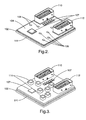
- the overmolded electronic assembly 100 of Fig. 1 is depicted prior to placement of the heat sinks 114 on the flip-chips 106 and after placement of the heat sinks 114 on the flip-chips 106, respectively.
- the overmold material 120 is shown covering the component side of the substrate 104 and encompassing the heat sinks 114.
- an overmolded electronic assembly has been described herein, which advantageously allows for the utilization of high thermally conductive heat sinks made of materials such as copper.
- the electronic assembly is not subject to typical mold clamp and overmold material induced stresses, which can cause the assembly to prematurely fail.
- An overmolded electronic assembly constructed as disclosed herein is particularly advantageous when utilized in the automotive environment, which increasingly requires assemblies to perform under environmental extremes.
Landscapes
- Engineering & Computer Science (AREA)
- Microelectronics & Electronic Packaging (AREA)
- Cooling Or The Like Of Semiconductors Or Solid State Devices (AREA)
- Structures Or Materials For Encapsulating Or Coating Semiconductor Devices Or Solid State Devices (AREA)
Applications Claiming Priority (1)
| Application Number | Priority Date | Filing Date | Title |
|---|---|---|---|
| US11/045,211 US7230829B2 (en) | 2005-01-28 | 2005-01-28 | Overmolded electronic assembly with insert molded heat sinks |
Publications (2)
| Publication Number | Publication Date |
|---|---|
| EP1686844A2 true EP1686844A2 (de) | 2006-08-02 |
| EP1686844A3 EP1686844A3 (de) | 2010-03-03 |
Family
ID=36405978
Family Applications (1)
| Application Number | Title | Priority Date | Filing Date |
|---|---|---|---|
| EP06075075A Withdrawn EP1686844A3 (de) | 2005-01-28 | 2006-01-12 | Umgossene elektronische Baugruppe mit einsatzgeformten Wärmesenken |
Country Status (2)
| Country | Link |
|---|---|
| US (1) | US7230829B2 (de) |
| EP (1) | EP1686844A3 (de) |
Families Citing this family (14)
| Publication number | Priority date | Publication date | Assignee | Title |
|---|---|---|---|---|
| US20080084671A1 (en) * | 2006-10-10 | 2008-04-10 | Ronnie Dean Stahlhut | Electrical circuit assembly for high-power electronics |
| US7903417B2 (en) * | 2006-10-10 | 2011-03-08 | Deere & Company | Electrical circuit assembly for high-power electronics |
| US8560124B2 (en) | 2007-07-13 | 2013-10-15 | Cummins Inc. | Idle control system and method for adaptive temperature control |
| US8078339B2 (en) * | 2007-07-13 | 2011-12-13 | Cummins Inc. | Circuit board with integrated connector |
| US7603770B2 (en) * | 2007-09-28 | 2009-10-20 | Delphi Technologies, Inc. | Method of overmolding an electronic assembly having an insert-molded vertical mount connector header |
| US7739791B2 (en) * | 2007-10-26 | 2010-06-22 | Delphi Technologies, Inc. | Method of producing an overmolded electronic module with a flexible circuit pigtail |
| US20090268414A1 (en) * | 2008-04-23 | 2009-10-29 | Bo Lu | Over-molded electronic module |
| US8081466B2 (en) * | 2009-07-06 | 2011-12-20 | Rockwell Automation Technologies, Inc. | Overmolded electronics enclosure |
| JP2011100718A (ja) * | 2009-10-05 | 2011-05-19 | Yazaki Corp | コネクタ |
| US8555493B2 (en) * | 2010-04-23 | 2013-10-15 | Psion, Inc. | Method of manufacturing a molded printed circuit board |
| CA2978795A1 (en) | 2015-03-16 | 2016-09-22 | Dana Canada Corporation | Heat exchangers with plates having surface patterns for enhancing flatness and methods for manufacturing same |
| CN108934132B (zh) * | 2017-05-25 | 2021-08-06 | 法雷奥汽车内部控制(深圳)有限公司 | 印刷电路板组件及其封装方法和机动车辆 |
| US11088066B2 (en) * | 2018-03-19 | 2021-08-10 | Tactotek Oy | Multilayer structure and related method of manufacture for electronics |
| GB2627962A (en) * | 2023-03-08 | 2024-09-11 | Continental Automotive Tech Gmbh | Electronic device for a vehicle |
Citations (1)
| Publication number | Priority date | Publication date | Assignee | Title |
|---|---|---|---|---|
| US20040012914A1 (en) * | 2002-07-17 | 2004-01-22 | International Business Machines Corporation | Electronic device substrate assembly with multilayer impermeable barrier and method of making |
Family Cites Families (10)
| Publication number | Priority date | Publication date | Assignee | Title |
|---|---|---|---|---|
| US4926241A (en) * | 1988-02-19 | 1990-05-15 | Microelectronics And Computer Technology Corporation | Flip substrate for chip mount |
| US5175612A (en) * | 1989-12-19 | 1992-12-29 | Lsi Logic Corporation | Heat sink for semiconductor device assembly |
| DE19506664A1 (de) * | 1995-02-25 | 1996-02-29 | Bosch Gmbh Robert | Elektrisches Gerät |
| US6180045B1 (en) * | 1998-05-20 | 2001-01-30 | Delco Electronics Corporation | Method of forming an overmolded electronic assembly |
| DE19910500A1 (de) * | 1999-03-10 | 2000-10-05 | Bosch Gmbh Robert | Elektrisches Gerät |
| US6307749B1 (en) * | 2000-10-23 | 2001-10-23 | Delphi Technologies, Inc. | Overmolded electronic module with underfilled surface-mount components |
| US6693239B2 (en) * | 2001-09-06 | 2004-02-17 | Delphi Technologies Inc. | Overmolded circuit board with underfilled surface-mount component and method therefor |
| US6807731B2 (en) * | 2002-04-02 | 2004-10-26 | Delphi Technologies, Inc. | Method for forming an electronic assembly |
| US6779260B1 (en) * | 2003-03-28 | 2004-08-24 | Delphi Technologies, Inc. | Overmolded electronic package including circuit-carrying substrate |
| US7132746B2 (en) * | 2003-08-18 | 2006-11-07 | Delphi Technologies, Inc. | Electronic assembly with solder-bonded heat sink |
-
2005
- 2005-01-28 US US11/045,211 patent/US7230829B2/en not_active Expired - Lifetime
-
2006
- 2006-01-12 EP EP06075075A patent/EP1686844A3/de not_active Withdrawn
Patent Citations (1)
| Publication number | Priority date | Publication date | Assignee | Title |
|---|---|---|---|---|
| US20040012914A1 (en) * | 2002-07-17 | 2004-01-22 | International Business Machines Corporation | Electronic device substrate assembly with multilayer impermeable barrier and method of making |
Also Published As
| Publication number | Publication date |
|---|---|
| US7230829B2 (en) | 2007-06-12 |
| US20060171120A1 (en) | 2006-08-03 |
| EP1686844A3 (de) | 2010-03-03 |
Similar Documents
| Publication | Publication Date | Title |
|---|---|---|
| US7230829B2 (en) | Overmolded electronic assembly with insert molded heat sinks | |
| US7708584B2 (en) | Semiconductor circuit arrangement | |
| US7473585B2 (en) | Technique for manufacturing an overmolded electronic assembly | |
| US9680273B2 (en) | Electrical connector with electrical contacts protected by a layer of compressible material and method of making it | |
| US20090139690A1 (en) | Heat sink and method for producing a heat sink | |
| CN105265031A (zh) | 电气控制设备 | |
| US11621212B2 (en) | Backing plate with manufactured features on top surface | |
| US20080233771A1 (en) | Customizable backer for achieving consistent loading and engagement of array package connections | |
| US6154365A (en) | Spring fixture that attaches a heat sink to a substrate for multiple cycle assembly/disassembly | |
| CN102812549A (zh) | 结合热沉使用的热塞及其组装方法 | |
| US5033970A (en) | Self-mounted chip carrier | |
| US7443026B2 (en) | IC chip package having force-adjustable member between stiffener and printed circuit board | |
| US7268429B2 (en) | Technique for manufacturing an overmolded electronic assembly | |
| US6905349B1 (en) | Technique for connector to printed circuit board decoupling to eliminate flexure | |
| US12266874B2 (en) | Thermal connection between printed circuit board and base plate with epoxy molded material | |
| US8546192B2 (en) | System for clamping heat sink | |
| US20110222245A1 (en) | Electronic module with center mounting fasteners | |
| US9402320B2 (en) | Electronic component assembly | |
| CN201628910U (zh) | 芯片模组压力调节装置 | |
| US20200321268A1 (en) | Robust Electronics Mounting Device | |
| US7482688B2 (en) | Attaching heat sinks to integrated circuit packages | |
| JP2004538602A (ja) | ランド・グリッド・アレイ・コネクタ用の取外し可能締め付け手段 | |
| JPS6365657A (ja) | ピングリツドアレイ | |
| EP3840556A1 (de) | Wärmeableitungsstruktur und elektronische vorrichtung | |
| JP2008159306A (ja) | コンプレッション型コネクタ |
Legal Events
| Date | Code | Title | Description |
|---|---|---|---|
| PUAI | Public reference made under article 153(3) epc to a published international application that has entered the european phase |
Free format text: ORIGINAL CODE: 0009012 |
|
| AK | Designated contracting states |
Kind code of ref document: A2 Designated state(s): AT BE BG CH CY CZ DE DK EE ES FI FR GB GR HU IE IS IT LI LT LU LV MC NL PL PT RO SE SI SK TR |
|
| AX | Request for extension of the european patent |
Extension state: AL BA HR MK YU |
|
| PUAL | Search report despatched |
Free format text: ORIGINAL CODE: 0009013 |
|
| AK | Designated contracting states |
Kind code of ref document: A3 Designated state(s): AT BE BG CH CY CZ DE DK EE ES FI FR GB GR HU IE IS IT LI LT LU LV MC NL PL PT RO SE SI SK TR |
|
| AX | Request for extension of the european patent |
Extension state: AL BA HR MK YU |
|
| RIC1 | Information provided on ipc code assigned before grant |
Ipc: H01L 23/31 20060101ALI20100126BHEP Ipc: H01L 23/433 20060101ALI20100126BHEP Ipc: H05K 7/20 20060101AFI20060529BHEP |
|
| 17P | Request for examination filed |
Effective date: 20100903 |
|
| AKX | Designation fees paid |
Designated state(s): AT BE BG CH CY CZ DE DK EE ES FI FR GB GR HU IE IS IT LI LT LU LV MC NL PL PT RO SE SI SK TR |
|
| 17Q | First examination report despatched |
Effective date: 20101025 |
|
| STAA | Information on the status of an ep patent application or granted ep patent |
Free format text: STATUS: THE APPLICATION IS DEEMED TO BE WITHDRAWN |
|
| 18D | Application deemed to be withdrawn |
Effective date: 20160105 |