EP1684352A1 - Phase-change memory device and manufacturing process thereof - Google Patents
Phase-change memory device and manufacturing process thereof Download PDFInfo
- Publication number
- EP1684352A1 EP1684352A1 EP05425024A EP05425024A EP1684352A1 EP 1684352 A1 EP1684352 A1 EP 1684352A1 EP 05425024 A EP05425024 A EP 05425024A EP 05425024 A EP05425024 A EP 05425024A EP 1684352 A1 EP1684352 A1 EP 1684352A1
- Authority
- EP
- European Patent Office
- Prior art keywords
- region
- phase
- change
- memory
- metal
- Prior art date
- Legal status (The legal status is an assumption and is not a legal conclusion. Google has not performed a legal analysis and makes no representation as to the accuracy of the status listed.)
- Granted
Links
Images


Classifications
-
- H—ELECTRICITY
- H10—SEMICONDUCTOR DEVICES; ELECTRIC SOLID-STATE DEVICES NOT OTHERWISE PROVIDED FOR
- H10B—ELECTRONIC MEMORY DEVICES
- H10B63/00—Resistance change memory devices, e.g. resistive RAM [ReRAM] devices
- H10B63/30—Resistance change memory devices, e.g. resistive RAM [ReRAM] devices comprising selection components having three or more electrodes, e.g. transistors
-
- H—ELECTRICITY
- H10—SEMICONDUCTOR DEVICES; ELECTRIC SOLID-STATE DEVICES NOT OTHERWISE PROVIDED FOR
- H10B—ELECTRONIC MEMORY DEVICES
- H10B63/00—Resistance change memory devices, e.g. resistive RAM [ReRAM] devices
- H10B63/80—Arrangements comprising multiple bistable or multi-stable switching components of the same type on a plane parallel to the substrate, e.g. cross-point arrays
- H10B63/82—Arrangements comprising multiple bistable or multi-stable switching components of the same type on a plane parallel to the substrate, e.g. cross-point arrays the switching components having a common active material layer
-
- H—ELECTRICITY
- H10—SEMICONDUCTOR DEVICES; ELECTRIC SOLID-STATE DEVICES NOT OTHERWISE PROVIDED FOR
- H10N—ELECTRIC SOLID-STATE DEVICES NOT OTHERWISE PROVIDED FOR
- H10N70/00—Solid-state devices without a potential-jump barrier or surface barrier, and specially adapted for rectifying, amplifying, oscillating or switching
- H10N70/20—Multistable switching devices, e.g. memristors
- H10N70/231—Multistable switching devices, e.g. memristors based on solid-state phase change, e.g. between amorphous and crystalline phases, Ovshinsky effect
-
- H—ELECTRICITY
- H10—SEMICONDUCTOR DEVICES; ELECTRIC SOLID-STATE DEVICES NOT OTHERWISE PROVIDED FOR
- H10N—ELECTRIC SOLID-STATE DEVICES NOT OTHERWISE PROVIDED FOR
- H10N70/00—Solid-state devices without a potential-jump barrier or surface barrier, and specially adapted for rectifying, amplifying, oscillating or switching
- H10N70/801—Constructional details of multistable switching devices
- H10N70/821—Device geometry
- H10N70/826—Device geometry adapted for essentially vertical current flow, e.g. sandwich or pillar type devices
-
- H—ELECTRICITY
- H10—SEMICONDUCTOR DEVICES; ELECTRIC SOLID-STATE DEVICES NOT OTHERWISE PROVIDED FOR
- H10N—ELECTRIC SOLID-STATE DEVICES NOT OTHERWISE PROVIDED FOR
- H10N70/00—Solid-state devices without a potential-jump barrier or surface barrier, and specially adapted for rectifying, amplifying, oscillating or switching
- H10N70/801—Constructional details of multistable switching devices
- H10N70/841—Electrodes
- H10N70/8413—Electrodes adapted for resistive heating
-
- H—ELECTRICITY
- H10—SEMICONDUCTOR DEVICES; ELECTRIC SOLID-STATE DEVICES NOT OTHERWISE PROVIDED FOR
- H10N—ELECTRIC SOLID-STATE DEVICES NOT OTHERWISE PROVIDED FOR
- H10N70/00—Solid-state devices without a potential-jump barrier or surface barrier, and specially adapted for rectifying, amplifying, oscillating or switching
- H10N70/801—Constructional details of multistable switching devices
- H10N70/881—Switching materials
- H10N70/882—Compounds of sulfur, selenium or tellurium, e.g. chalcogenides
- H10N70/8828—Tellurides, e.g. GeSbTe
Definitions
- the present invention relates to a phase-change memory (PCM) device and the manufacturing process thereof.
- PCM phase-change memory
- phase-change memory devices are based upon storage elements which use a class of materials that have the property of switching between two phases having distinct electrical characteristics, associated to two different crystallographic structures of the material forming the storage element, namely a disorderly amorphous phase and an orderly crystalline or polycrystalline phase.
- the alloys of the elements of group VI of the periodic table such as Te or Se, referred to as calcogenides or calcogenic materials, may be advantageously used in phase-change memory cells.
- the currently most promising calcogenide is formed by an alloy of Ge, Sb, and Te (Ge 2 Sb 2 Te 5 ), which is now widely used for storing information in over-writeable disks.
- the resistivity varies by two or more orders of magnitude when the material passes from the amorphous phase (which is more resistive) to the crystalline one (which is more conductive), and vice versa.
- the phase change can be obtained by increasing the temperature locally. Below 150°C, both the phases are stable. Above 200°C, starting from the amorphous phase, there is a rapid nucleation of the crystallites and, if the material is kept at the crystallization temperature for a sufficient time, it changes phase and becomes crystalline. To bring the calcogenide back into the amorphous state, it is necessary to raise the temperature above the melting point (approximately 600°C) and then cool the calcogenide rapidly.
- the structure of a phase-change memory array, which uses a calcogenic element as the storage element, is illustrated in Figure 1.
- the memory array 1 of Figure 1 comprises a plurality of memory cells 2, each including a storage element 3 of a phase-change type and a selection element 4 formed here by an NMOS transistor.
- the selection element 4 can be formed by a bipolar-junction transistor, by a PN diode or by a calcogenic switch ("ovonic threshold switch").
- the invention relates to a memory array wherein the selection element 4 is made as an MOS transistor, to which reference will then be made hereinafter.
- the memory cells 2 are arranged in rows and columns.
- the storage element 3 has a first terminal connected to an own bitline 6 (address bitlines BLn-1, BLn, ...), and a second terminal connected to a first conduction terminal of an own selection element 4.
- the selection element 4 has a control terminal connected to an own control line, also referred to as a wordline 7 (address wordlines WLn-1, WLn, ...) and a grounded second conduction terminal.
- the storage element 3 is formed by a portion of a region of calcogenic material (which forms the proper memory portion) and by a heating element that enables the phase change.
- Figure 2 shows the cross-section through a wafer of conductive material wherein a memory cell 2 has been formed.
- a wafer 10 comprises a substrate 11 of a P type accommodating a source region 12 and a drain region 13 of an N+ type.
- the source and drain regions 12, 13 are reciprocally spaced by a portion 14 of the substrate, which forms a channel region.
- a gate region 15 (formed by a wordline 7 of Figure 1) extends on top of the substrate 11, vertically aligned to the channel region 14, but isolated with respect to the substrate 11.
- the source region 12, the drain region 13 and the gate region 15 form an MOS device forming the selection element 4 of Figure 1.
- a dielectric region 18 extends on top of the substrate 11 and accommodates within it, in addition to the gate region 15, a source line 19, a drain contact 20, a heating element 21, and a bitline 22.
- the source line 19 is formed by a local interconnection line (LIL), which extends transversely with respect to the drawing plane (parallel to the wordline 7) and connects the source regions 12 of the memory cells 2 arranged on a same row of the memory array 1 of Figure 1.
- LIL local interconnection line
- the different source lines 19 of memory cells 2 belonging to a same sector are moreover connected to one another and to ground (as represented in the equivalent electrical circuit of Figure 1).
- the source line 19 is obtained using a contact technique, forming a via in the bottom portion of the dielectric layer 18 and filling the via with conductive material, for example tungsten, possibly coated with a barrier material, such as Ti/TiN.
- the drain contact 20 is made simultaneously and using the same technique as the source line 19, albeit having a different area, of a square or circular shape, and thus it has the same cross-section as the source line 19 in the cross-sectional view of Figure 2 (in particular, it has the same height) but differs in a section perpendicular thereto.
- the heating element 21 is made of a resistive material having thermal stability and good compatibility with CMOS processes and with calcogenic materials.
- a resistive material having thermal stability and good compatibility with CMOS processes and with calcogenic materials.
- TiSiN, TiAlN or TiSiC can be used, formed as a thin layer that coats the walls of a cavity formed in an intermediate portion of the dielectric layer 18. The cavity is then filled with dielectric material.
- the bitline 22 preferably comprises a multilayer including at least one calcogenic layer 22a (for example, of Ge 2 Sb 2 Te 5 ) and a metal electrode layer 22b (for example, of AlCu); an adhesive layer may moreover be provided (for example, of Ti or Si) underneath the calcogenic layer 22a and/or a barrier layer may be provided on top of the calcogenic layer 22a.
- calcogenic layer 22a for example, of Ge 2 Sb 2 Te 5
- a metal electrode layer 22b for example, of AlCu
- an adhesive layer may moreover be provided (for example, of Ti or Si) underneath the calcogenic layer 22a and/or a barrier layer may be provided on top of the calcogenic layer 22a.
- the heating element 21, the drain contact 20 (and thus the source line 19), and the bitline 22 can be obtained as described in detail, for example, in EP-A-1 318 552 or in EP-A-1 339 110, which refer, however, to the construction of memory cells having a selection element of a bipolar type.
- the aim of the invention is thus to provide a device and a manufacturing process that can be implemented with any currently used or future, CMOS-compatible technique.
- phase-change memory device and the manufacturing process thereof are provided, as defined in claims 1 and 11, respectively.
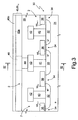
- Figures 3-5 refer to an embodiment wherein the source line is made in a metal layer, and precisely in the first metal level (metal1). Furthermore, the bitline is formed on top of the first metal level, and precisely between the first and second metal levels (not illustrated). Furthermore, the memory cells are split-gate cells, i.e., the selection element 4 is formed by two MOS transistors connected in parallel and thus equivalent to an individual MOS transistor having a width W twice the width of the defined active area.
- a wafer 30 comprises a substrate 31 of a P type accommodating source regions 32 (two of which are visible in Figure 3) and drain regions 33 (just one of which is visible in Figure 3). Between each source region 32 and the adjacent drain region 33, the substrate 31 forms a channel region 34; a dielectric layer 35 coats all the surface of the substrate 31 and accommodates gate regions 36 that extend on the channel regions 34 and are formed by polysilicon lines WL forming the wordlines 7 of Figure 1.
- Source-contact regions 40 extend through the dielectric layer 35 between the source regions 32 and the source lines 42; likewise, drain-contact regions or memory-contact regions 41 extend between the drain regions 33 and the metal pad regions 43.
- the source-contact regions 40 and drain-contact regions 41 are made in vias opened in the bottom portion of the dielectric layer 35 and are obtained using the contact technique, for example, with tungsten coated with a Ti/TiN barrier layer.
- each source-contact region 40 defines a local contact with a respective source region 32, and the connection between the various source regions 32 is ensured by the source lines 42, which extend at a certain height on top of the substrate and are distinct from the source-contact regions 40 themselves.
- the source lines 42 and the metal pad regions 43 are formed in the first metal level (metal1) which is for example of AlCu or Cu, and have the shape shown in the top view of Figure 5; in particular, the source lines 42 extend parallel to the wordlines WL, while the metal pad regions 43 have a rectangular or square shape.
- metal1 which is for example of AlCu or Cu
- Heater elements 44 of resistive material, extend on top of the metal pad regions 43. Finally, bitlines 45 are formed on top of the heater elements 44, locally in contact with the heater elements 44.
- the bitlines 45 are formed by a bottom layer 45a, of calcogenic material, and by a top layer 45b, of metal material, for example AlCu or Cu.
- Figures 3 and 5 show in a complete way just one memory cell 2, comprising a column 41, 43, 44, a drain region 33, two gate regions 36 (wordlines WL n ), and two source regions 32; the source regions 32 are moreover shared with the adjacent memory cells 2, connected to the wordlines WL n-1 and WL n+1 .
- each heating element 44 could be formed by a wall of material deposited in an appropriate cavity
- the bitlines 45 could comprise further layers, such as an adhesion layer and/or a barrier layer and could be shaped so as to have a thinner bottom portion.
- the bottom layer 45a could be formed by a thin line that crosses the walls forming the heater elements.
- the structure of the heater elements 44 and of the bitlines 45 could correspond to the one illustrated in the drawings.
- the portions of the bottom layer 45a of the bitlines 45 in contact with the heater elements 44 form storage regions, designated as a whole by 46, the phase whereof (whether crystalline or amorphous) represents the information stored.
- the line 48 represents the active-area mask which, in this embodiment, is strip-shaped and extends through the entire column. Furthermore, field-isolation regions 49 are visible in the cross-section of Figure 4 (preferably formed through shallow-trench isolation - STI), and separate cells 2 that are adjacent in the direction of the wordlines WL (and thus of the source lines 42).
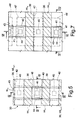
- Figures 6 and 7 refer to a different embodiment of the invention, referred to as split-active, wherein the active areas 48' are formed by rectangles of width W, corresponding to two adjacent memory cells 2.
- each active area accommodates two drain regions 33 and a single source region 32, which is intermediate and is shared by the two memory cells 2.
- the cross-section perpendicular to that of Figure 6 coincides with that of Figure 4.
- Figures 3-5 and 6-7 are both characterized in that the definition of the storage element 46 occurs after definition of the metal1 level, and the heater elements 44 are defined between the metal1 level and the bitlines 45.
- This approach has the main advantage of reducing the thermal budget seen by the bottom layer 45a, of calcogenic material, of the bitlines 45, maintaining the same basic architecture of traditional memory cells 2, and thus without having to modify excessively the existing design criteria.
- the second metal level (meta12, not illustrated) can be advantageously used for strapping of the wordlines WL, in a per se known manner.
- the use of the first solution or of the second solution depends upon the technology adopted (layout rules) and upon the sizing of the MOS transistor (width W and length L of the gate); in practice, the two solutions provide different shape factors (i.e., the ratio between global width and length of each cell), and during the design phase it is possible to use the optimal solution for the required specifications.
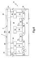
- Figures 8-10 show a third embodiment, wherein the storage region 46 is not formed by the bitline 45 but by an appropriate region (rectangular dot or pad) set underneath the metal1 level. Furthermore, the third embodiment implements a solution of the split-gate type, like the first embodiment.
- the third embodiment has a similar top view as the embodiment of Figure 5, except, as mentioned, for the shape of the regions of calcogenic material, consequently the top view is not illustrated.
- the source-contact regions 40 are formed by different parts and comprise a bottom portion 40a, equivalent to the contact region 40 of Figures 3-7, and a top portion 40b, formed using the same technique and aligned to the bottom portion 40a, thereby, globally, the source-contact regions 40 of Figures 8 and 9 have a height greater than the height of those of Figures 3-7.
- the heater elements 44 are formed immediately on top of the drain-contact or memory regions 41; the storage regions 46 (of calcogenic material) are arranged immediately on top of the heater elements 44; and first contact portions 50 are formed on top of the storage regions 46 and extend up to the level of the metal1 level.
- Metal pad regions 43 are here formed on top of the first contact portions 50, at the same height as the source lines 42, since both the source lines 42 and the metal pad regions 43 are formed in the first metal level (metal1).
- second contact portions 51 are present, which connect the metal pad regions 43 and thus the storage regions 46 to the bitlines 45, which are here formed by the second metal level (metal2) and are obtained with the techniques normally used for metal interconnections (for example, AlCu or Cu interconnections).
- the source-contact regions 40 are made by two different portions 40a, 40b, arranged on top of one another and made at two different times, the first portions 40a using the contact technique, before the formation of the heater elements 44, and the second portions 40b using the same contact technique, after the formation of the storage regions 46, and the deposition and planarization of an intermediate portion of the dielectric layer 35, together with the first contact portions 50.
- bitlines 45 are formed.
- Figure 10 shows an embodiment differring from the third embodiment of Figures 8-9, of the split-active type wherein, similarly to the embodiment of Figures 6 and 7, the active-area mask has separate windows for each memory cell 2.
- the cross-section perpendicular to Figure 10 is the same as in Figure 9 and the top view is similar to Figure 7 (apart from the shape of the region of calcogenic material), and consequently said views are not shown.
- the third and fourth embodiments illustrated in Figures 8-10 have the advantage that the storage regions 46 are separated from the bitlines 45 and can be located only where necessary. In this way, it is possible to avoid some process steps (such as deposition and definition of the top metal layer 45b, on top of the calcogenic material 45a), which are, instead, necessary for the first and second embodiments for reducing the resistivity of the bitlines 45.
- FIG 11 shows a portion of a system 500 according to an embodiment of the present invention.
- the system 500 can be used in wireless devices such as, for example, a personal digital assistant (PDA), a laptop or portable computer with wireless capacity, a "web tablet", a wireless telephone, a pager, a device for sending instantaneous messages, a digital music player, a digital camcorder, or other devices that can be suitable for transmitting and/or receiving information in wireless mode.
- PDA personal digital assistant
- the system 500 can be used in any one of the following systems: a wireless local area network (WLAN) system, a wireless personal area network (WPAN) system, or a cellphone network, even though the extent of the present invention is not limited in this connection.
- WLAN wireless local area network
- WPAN wireless personal area network
- cellphone network even though the extent of the present invention is not limited in this connection.
- the system 500 comprises a controller 510, an I/O device 520 (for example, a keyboard or a display), a memory 530, a wireless interface 540, and a static random-access memory (SRAM) 560, connected to one another through a bus 550.
- a battery 580 supplies the system 500.
- the controller 510 comprises, for example, one or more microprocessors, digital signal processors, microcontrollers, or the like.
- the memory 1 can be used for storing messages transmitted to or received by a system 500.
- the memory 1 can optionally be used also for storing instructions that are executed by the controller 510 during operation of the system 500, and can be used for storing user data.
- the instructions can be stored as digital information, and the user data, as described herein, can be stored in one section of the memory as digital data and, in another section, as analog memory. In another example, one data section at a time can be labeled as such and can store digital information, and can then be re-labeled and reconfigured for storing analog information.
- the memory 530 can be provided with one or more types of memory.
- the memory 530 can comprise a volatile memory (any type of RAM), a nonvolatile memory, such as a flash memory, and/or a memory that includes the memory array 1 of Figure 1.
- the I/O device 520 can be used for generating a message.
- the system 500 can use the wireless interface 540 for transmitting and receiving messages to and from a wireless communication network with a radio-frequency (RF) signal.
- wireless interfaces 540 comprise an antenna or a wireless transceiver, such as a dipole antenna, even though the scope of the present invention is not limited in this respect.
- the I/O device 520 can provide a voltage reflecting what is stored as either a digital output (if digital information was stored), or as analog information (if analog information was stored).
Abstract
Description
- The present invention relates to a phase-change memory (PCM) device and the manufacturing process thereof.
- As is known, phase-change memory devices are based upon storage elements which use a class of materials that have the property of switching between two phases having distinct electrical characteristics, associated to two different crystallographic structures of the material forming the storage element, namely a disorderly amorphous phase and an orderly crystalline or polycrystalline phase.
- Currently, the alloys of the elements of group VI of the periodic table, such as Te or Se, referred to as calcogenides or calcogenic materials, may be advantageously used in phase-change memory cells. The currently most promising calcogenide is formed by an alloy of Ge, Sb, and Te (Ge2Sb2Te5), which is now widely used for storing information in over-writeable disks.
- In the calcogenides, the resistivity varies by two or more orders of magnitude when the material passes from the amorphous phase (which is more resistive) to the crystalline one (which is more conductive), and vice versa.
- The phase change can be obtained by increasing the temperature locally. Below 150°C, both the phases are stable. Above 200°C, starting from the amorphous phase, there is a rapid nucleation of the crystallites and, if the material is kept at the crystallization temperature for a sufficient time, it changes phase and becomes crystalline. To bring the calcogenide back into the amorphous state, it is necessary to raise the temperature above the melting point (approximately 600°C) and then cool the calcogenide rapidly.
- From the electrical standpoint, it is possible to reach the crystallization and melting temperatures by causing a current to flow through a resistive element (also referred to as a heater), which heats the calcogenic material by the Joule effect.
- The structure of a phase-change memory array, which uses a calcogenic element as the storage element, is illustrated in Figure 1. The
memory array 1 of Figure 1 comprises a plurality ofmemory cells 2, each including astorage element 3 of a phase-change type and aselection element 4 formed here by an NMOS transistor. Alternatively, theselection element 4 can be formed by a bipolar-junction transistor, by a PN diode or by a calcogenic switch ("ovonic threshold switch"). - The invention relates to a memory array wherein the
selection element 4 is made as an MOS transistor, to which reference will then be made hereinafter. - The
memory cells 2 are arranged in rows and columns. In eachmemory cell 2, thestorage element 3 has a first terminal connected to an own bitline 6 (address bitlines BLn-1, BLn, ...), and a second terminal connected to a first conduction terminal of anown selection element 4. Theselection element 4 has a control terminal connected to an own control line, also referred to as a wordline 7 (address wordlines WLn-1, WLn, ...) and a grounded second conduction terminal. - The
storage element 3 is formed by a portion of a region of calcogenic material (which forms the proper memory portion) and by a heating element that enables the phase change. - Figure 2 shows the cross-section through a wafer of conductive material wherein a
memory cell 2 has been formed. - In detail, a
wafer 10 comprises asubstrate 11 of a P type accommodating asource region 12 and adrain region 13 of an N+ type. The source anddrain regions portion 14 of the substrate, which forms a channel region. A gate region 15 (formed by a wordline 7 of Figure 1) extends on top of thesubstrate 11, vertically aligned to thechannel region 14, but isolated with respect to thesubstrate 11. Thesource region 12, thedrain region 13 and thegate region 15 form an MOS device forming theselection element 4 of Figure 1. - A
dielectric region 18 extends on top of thesubstrate 11 and accommodates within it, in addition to thegate region 15, asource line 19, adrain contact 20, aheating element 21, and abitline 22. - The
source line 19 is formed by a local interconnection line (LIL), which extends transversely with respect to the drawing plane (parallel to the wordline 7) and connects thesource regions 12 of thememory cells 2 arranged on a same row of thememory array 1 of Figure 1. Thedifferent source lines 19 ofmemory cells 2 belonging to a same sector are moreover connected to one another and to ground (as represented in the equivalent electrical circuit of Figure 1). In currently proposed devices, thesource line 19 is obtained using a contact technique, forming a via in the bottom portion of thedielectric layer 18 and filling the via with conductive material, for example tungsten, possibly coated with a barrier material, such as Ti/TiN. - Generally, the
drain contact 20 is made simultaneously and using the same technique as thesource line 19, albeit having a different area, of a square or circular shape, and thus it has the same cross-section as thesource line 19 in the cross-sectional view of Figure 2 (in particular, it has the same height) but differs in a section perpendicular thereto. - The
heating element 21 is made of a resistive material having thermal stability and good compatibility with CMOS processes and with calcogenic materials. For example, TiSiN, TiAlN or TiSiC can be used, formed as a thin layer that coats the walls of a cavity formed in an intermediate portion of thedielectric layer 18. The cavity is then filled with dielectric material. - The
bitline 22 preferably comprises a multilayer including at least onecalcogenic layer 22a (for example, of Ge2Sb2Te5) and ametal electrode layer 22b (for example, of AlCu); an adhesive layer may moreover be provided (for example, of Ti or Si) underneath thecalcogenic layer 22a and/or a barrier layer may be provided on top of thecalcogenic layer 22a. - The
heating element 21, the drain contact 20 (and thus the source line 19), and thebitline 22 can be obtained as described in detail, for example, in EP-A-1 318 552 or in EP-A-1 339 110, which refer, however, to the construction of memory cells having a selection element of a bipolar type. - The structure of Figure 2 has the disadvantage that it cannot implemented with all the currently available processes, in particular when the basic CMOS technology does not enable local interconnections of an LIL type to be made.
- The aim of the invention is thus to provide a device and a manufacturing process that can be implemented with any currently used or future, CMOS-compatible technique.
- According to the present invention, a phase-change memory device and the manufacturing process thereof are provided, as defined in
claims - For an understanding of the present invention a preferred embodiment thereof is now described, purely by way of nonlimiting example, with reference to the attached drawings, wherein:
- Figure 1 shows the equivalent electrical circuit of a phase-change memory array;
- Figure 2 shows the implementation of a cell of the memory of Figure 1;
- Figures 3-5 show two cross-sectional views and a top view of a first embodiment of a memory cell;
- Figures 6 and 7 show a cross-sectional view and a top view of a second embodiment of a memory cell;
- Figures 8 and 9 show two cross-sectional views of a third embodiment of a memory cell;
- Figure 10 shows a cross-sectional view of a fourth embodiment of a memory cell; and
- Figure 11 is a block diagram of a system that uses the present storage device.
- Figures 3-5 refer to an embodiment wherein the source line is made in a metal layer, and precisely in the first metal level (metal1). Furthermore, the bitline is formed on top of the first metal level, and precisely between the first and second metal levels (not illustrated). Furthermore, the memory cells are split-gate cells, i.e., the
selection element 4 is formed by two MOS transistors connected in parallel and thus equivalent to an individual MOS transistor having a width W twice the width of the defined active area. - In detail, a
wafer 30 comprises asubstrate 31 of a P type accommodating source regions 32 (two of which are visible in Figure 3) and drain regions 33 (just one of which is visible in Figure 3). Between eachsource region 32 and theadjacent drain region 33, thesubstrate 31 forms achannel region 34; adielectric layer 35 coats all the surface of thesubstrate 31 and accommodatesgate regions 36 that extend on thechannel regions 34 and are formed by polysilicon lines WL forming the wordlines 7 of Figure 1. - Source-
contact regions 40 extend through thedielectric layer 35 between thesource regions 32 and thesource lines 42; likewise, drain-contact regions or memory-contact regions 41 extend between thedrain regions 33 and themetal pad regions 43. - The source-
contact regions 40 and drain-contact regions 41 are made in vias opened in the bottom portion of thedielectric layer 35 and are obtained using the contact technique, for example, with tungsten coated with a Ti/TiN barrier layer. - In practice, each source-
contact region 40 defines a local contact with arespective source region 32, and the connection between thevarious source regions 32 is ensured by thesource lines 42, which extend at a certain height on top of the substrate and are distinct from the source-contact regions 40 themselves. - The
source lines 42 and themetal pad regions 43 are formed in the first metal level (metal1) which is for example of AlCu or Cu, and have the shape shown in the top view of Figure 5; in particular, thesource lines 42 extend parallel to the wordlines WL, while themetal pad regions 43 have a rectangular or square shape. -
Heater elements 44, of resistive material, extend on top of themetal pad regions 43. Finally,bitlines 45 are formed on top of theheater elements 44, locally in contact with theheater elements 44. - The
bitlines 45 are formed by abottom layer 45a, of calcogenic material, and by atop layer 45b, of metal material, for example AlCu or Cu. - In practice, Figures 3 and 5 show in a complete way just one
memory cell 2, comprising acolumn drain region 33, two gate regions 36 (wordlines WLn), and twosource regions 32; thesource regions 32 are moreover shared with theadjacent memory cells 2, connected to the wordlines WLn-1 and WLn+1. - It is emphasized that Figures 3-5 are only schematic as regards the
heater elements 44 and thebitlines 45, and these could be modified as described in the European patents cited above so as to obtain sublithographic contact regions. For example, eachheating element 44 could be formed by a wall of material deposited in an appropriate cavity, and thebitlines 45 could comprise further layers, such as an adhesion layer and/or a barrier layer and could be shaped so as to have a thinner bottom portion. For example, thebottom layer 45a could be formed by a thin line that crosses the walls forming the heater elements. Alternatively, should considerations of a thermal type not require the presence of submicrometric contact regions between the heating material and the calcogenic material, the structure of theheater elements 44 and of thebitlines 45 could correspond to the one illustrated in the drawings. - In any case, the portions of the
bottom layer 45a of thebitlines 45 in contact with theheater elements 44 form storage regions, designated as a whole by 46, the phase whereof (whether crystalline or amorphous) represents the information stored. - For completeness, it is pointed out that, in the top view of Figure 5, the
line 48 represents the active-area mask which, in this embodiment, is strip-shaped and extends through the entire column. Furthermore, field-isolation regions 49 are visible in the cross-section of Figure 4 (preferably formed through shallow-trench isolation - STI), andseparate cells 2 that are adjacent in the direction of the wordlines WL (and thus of the source lines 42). - Figures 6 and 7 refer to a different embodiment of the invention, referred to as split-active, wherein the active areas 48' are formed by rectangles of width W, corresponding to two
adjacent memory cells 2. In practice, here, each active area accommodates twodrain regions 33 and asingle source region 32, which is intermediate and is shared by the twomemory cells 2. In this case, the cross-section perpendicular to that of Figure 6 coincides with that of Figure 4. - The embodiments of Figures 3-5 and 6-7 are both characterized in that the definition of the
storage element 46 occurs after definition of the metal1 level, and theheater elements 44 are defined between the metal1 level and thebitlines 45. This approach has the main advantage of reducing the thermal budget seen by thebottom layer 45a, of calcogenic material, of thebitlines 45, maintaining the same basic architecture oftraditional memory cells 2, and thus without having to modify excessively the existing design criteria. - Furthermore, with the presented solutions it is possible to save a mask (LIL or pre-contact mask), if this is not required by the basic CMOS process.
- In these two cases, the second metal level (meta12, not illustrated) can be advantageously used for strapping of the wordlines WL, in a per se known manner. The use of the first solution or of the second solution depends upon the technology adopted (layout rules) and upon the sizing of the MOS transistor (width W and length L of the gate); in practice, the two solutions provide different shape factors (i.e., the ratio between global width and length of each cell), and during the design phase it is possible to use the optimal solution for the required specifications.
- Figures 8-10 show a third embodiment, wherein the
storage region 46 is not formed by thebitline 45 but by an appropriate region (rectangular dot or pad) set underneath the metal1 level. Furthermore, the third embodiment implements a solution of the split-gate type, like the first embodiment. The third embodiment has a similar top view as the embodiment of Figure 5, except, as mentioned, for the shape of the regions of calcogenic material, consequently the top view is not illustrated. - In detail, in Figures 8 and 9, the source-
contact regions 40 are formed by different parts and comprise abottom portion 40a, equivalent to thecontact region 40 of Figures 3-7, and atop portion 40b, formed using the same technique and aligned to thebottom portion 40a, thereby, globally, the source-contact regions 40 of Figures 8 and 9 have a height greater than the height of those of Figures 3-7. - Furthermore, the
heater elements 44 are formed immediately on top of the drain-contact ormemory regions 41; the storage regions 46 (of calcogenic material) are arranged immediately on top of theheater elements 44; andfirst contact portions 50 are formed on top of thestorage regions 46 and extend up to the level of the metal1 level.Metal pad regions 43 are here formed on top of thefirst contact portions 50, at the same height as the source lines 42, since both the source lines 42 and themetal pad regions 43 are formed in the first metal level (metal1). - On top of the
metal pad regions 43,second contact portions 51 are present, which connect themetal pad regions 43 and thus thestorage regions 46 to thebitlines 45, which are here formed by the second metal level (metal2) and are obtained with the techniques normally used for metal interconnections (for example, AlCu or Cu interconnections). - In practice, since the
storage regions 46 are here made separately from thebitlines 45, underneath the metal1 level, the source-contact regions 40 are made by twodifferent portions first portions 40a using the contact technique, before the formation of theheater elements 44, and thesecond portions 40b using the same contact technique, after the formation of thestorage regions 46, and the deposition and planarization of an intermediate portion of thedielectric layer 35, together with thefirst contact portions 50. After formation of the source lines 42, of themetal pad regions 43, and possibly of other regions in the first metal level (metal1), deposition and planarization of a further portion of thedielectric layer 35, and formation of the second contact portions 51 (also these formed using the contact technique), thebitlines 45 are formed. - Figure 10 shows an embodiment differring from the third embodiment of Figures 8-9, of the split-active type wherein, similarly to the embodiment of Figures 6 and 7, the active-area mask has separate windows for each
memory cell 2. In this fourth embodiment, the cross-section perpendicular to Figure 10 is the same as in Figure 9 and the top view is similar to Figure 7 (apart from the shape of the region of calcogenic material), and consequently said views are not shown. - The third and fourth embodiments illustrated in Figures 8-10 have the advantage that the
storage regions 46 are separated from thebitlines 45 and can be located only where necessary. In this way, it is possible to avoid some process steps (such as deposition and definition of thetop metal layer 45b, on top of thecalcogenic material 45a), which are, instead, necessary for the first and second embodiments for reducing the resistivity of thebitlines 45. - Figure 11 shows a portion of a
system 500 according to an embodiment of the present invention. Thesystem 500 can be used in wireless devices such as, for example, a personal digital assistant (PDA), a laptop or portable computer with wireless capacity, a "web tablet", a wireless telephone, a pager, a device for sending instantaneous messages, a digital music player, a digital camcorder, or other devices that can be suitable for transmitting and/or receiving information in wireless mode. Thesystem 500 can be used in any one of the following systems: a wireless local area network (WLAN) system, a wireless personal area network (WPAN) system, or a cellphone network, even though the extent of the present invention is not limited in this connection. - The
system 500 comprises acontroller 510, an I/O device 520 (for example, a keyboard or a display), amemory 530, awireless interface 540, and a static random-access memory (SRAM) 560, connected to one another through abus 550. Abattery 580 supplies thesystem 500. - The
controller 510 comprises, for example, one or more microprocessors, digital signal processors, microcontrollers, or the like. Thememory 1 can be used for storing messages transmitted to or received by asystem 500. Thememory 1 can optionally be used also for storing instructions that are executed by thecontroller 510 during operation of thesystem 500, and can be used for storing user data. The instructions can be stored as digital information, and the user data, as described herein, can be stored in one section of the memory as digital data and, in another section, as analog memory. In another example, one data section at a time can be labeled as such and can store digital information, and can then be re-labeled and reconfigured for storing analog information. Thememory 530 can be provided with one or more types of memory. For example, thememory 530 can comprise a volatile memory (any type of RAM), a nonvolatile memory, such as a flash memory, and/or a memory that includes thememory array 1 of Figure 1. - The I/
O device 520 can be used for generating a message. Thesystem 500 can use thewireless interface 540 for transmitting and receiving messages to and from a wireless communication network with a radio-frequency (RF) signal. Examples ofwireless interfaces 540 comprise an antenna or a wireless transceiver, such as a dipole antenna, even though the scope of the present invention is not limited in this respect. Furthermore, the I/O device 520 can provide a voltage reflecting what is stored as either a digital output (if digital information was stored), or as analog information (if analog information was stored). - Finally, it is clear that numerous modifications and variations can be made to the storage device and to the manufacturing process described and illustrated herein, all of which fall within the scope of the invention, as defined in the attached claims.
Claims (11)
- A phase-change memory device, comprising an array (1) of memory cells (2) arranged in rows (7) and columns (6) and each including a selection device (4) of an MOS type and a phase-change region (3) connected to said selection device, said selection device (4) having a first conductive region (32) and a second conductive region (33), formed in a substrate (31) of semiconductor material and spaced from one another by a channel region (34), and an isolated control region (36) connected to a respective one of said rows (7) of said array and overlying said channel region (34); said first conductive region (32) being connected to a connection line (42) extending parallel to said rows, said second conductive region (33) being connected to said phase-change region (46), and said phase-change region being connected to a respective one of said columns (6) of said array; characterized in that said first connection line (42) is a metal interconnection line and is connected to said first conductive region (32) via a source-contact region (40), distinct from said first connection line (42).
- The device according to claim 1, wherein said metal interconnection line (42) is formed in a metal level.
- The device according to claim 2, wherein said metal level is a first metal level.
- The device according to claim 3, wherein said second conductive region (33) is connected to said phase-change region (46) through a memory-contact region (41) and a metal-pad region (43) formed in said first metal level and aligned horizontally with said metal interconnection line (42).
- The device according to claim 4, wherein said column (6) comprises a strip (45a) of phase-change material extending on top of said first metal level, a heating element (44) extending between said metal-pad region (43) and said strip of phase-change material (45a).
- The device according to claim 5, wherein a metal strip (45b) extends on top of said strip of phase-change material (45a).
- The device according to claim 3, wherein said second conductive region (33) is connected to said phase-change region (46) through a memory-contact region (41), and said phase-change region (46) forms a dot and is connected to said column (45) through at least one first contact portion (50).
- The device according to claim 7, comprising a metal-pad region (43) formed in said first metal level and aligned horizontally with said metal interconnection line (42), said metal-pad region (43) being connected to said phase-change region (46) through said first contact portion (50) and to said column (45) through a second contact portion (51).
- The device according to claim 8, comprising a heating element (44) extending between said phase-change region (46) and said memory-contact region (41).
- The device according to any one of claims 7-9, wherein said column (45) is formed by a line of metal material formed in a second metal level and extends on top of said phase-change region (46) and said metal interconnection line (42).
- A manufacturing process of a phase-change memory device (530), comprising an array (1) of memory cells arranged in rows (7) and columns (6) and each including a selection device (4) of an MOS type and a phase-change region (3) connected to said selection device, the process comprising the steps of:forming a first and a second conductive region (32, 33) in a substrate (31) of semiconductor material, said first and second conductive regions being spaced from one another by a channel region (34);forming a wordline (7) defining an isolated control region (36), which extends on top of said channel region (14) parallel to said rows (7);forming at least one memory-contact region (41) on top of and electrically connected to said second conductive region (33);forming a phase-change region (46) on top of and electrically connected to said memory-contact region (41);forming a connection line (42) on top of and electrically connected to said first conductive region (32), said connection line (42) extending parallel to said wordline (7);characterized in that the step of forming a connection line (42) comprises forming first a source-contact region (40) on top of and in contact with said first conductive region (32) simultaneously with said memory-contact region (41);
and subsequently forming a metal interconnection line (42) distinct from said source-contact region (40) and extending parallel to said wordline (7).
Priority Applications (3)
| Application Number | Priority Date | Filing Date | Title |
|---|---|---|---|
| EP05425024A EP1684352B1 (en) | 2005-01-21 | 2005-01-21 | Phase-change memory device and manufacturing process thereof |
| DE602005009793T DE602005009793D1 (en) | 2005-01-21 | 2005-01-21 | Phase change memory device and method for its production |
| US11/337,787 US20060202245A1 (en) | 2005-01-21 | 2006-01-23 | Phase-change memory device and manufacturing process thereof |
Applications Claiming Priority (1)
| Application Number | Priority Date | Filing Date | Title |
|---|---|---|---|
| EP05425024A EP1684352B1 (en) | 2005-01-21 | 2005-01-21 | Phase-change memory device and manufacturing process thereof |
Publications (2)
| Publication Number | Publication Date |
|---|---|
| EP1684352A1 true EP1684352A1 (en) | 2006-07-26 |
| EP1684352B1 EP1684352B1 (en) | 2008-09-17 |
Family
ID=34943019
Family Applications (1)
| Application Number | Title | Priority Date | Filing Date |
|---|---|---|---|
| EP05425024A Active EP1684352B1 (en) | 2005-01-21 | 2005-01-21 | Phase-change memory device and manufacturing process thereof |
Country Status (3)
| Country | Link |
|---|---|
| US (1) | US20060202245A1 (en) |
| EP (1) | EP1684352B1 (en) |
| DE (1) | DE602005009793D1 (en) |
Cited By (1)
| Publication number | Priority date | Publication date | Assignee | Title |
|---|---|---|---|---|
| FR3056826A1 (en) * | 2016-09-28 | 2018-03-30 | St Microelectronics Crolles 2 Sas | MEMORY CELL WITH PHASE CHANGE |
Families Citing this family (31)
| Publication number | Priority date | Publication date | Assignee | Title |
|---|---|---|---|---|
| US7635855B2 (en) | 2005-11-15 | 2009-12-22 | Macronix International Co., Ltd. | I-shaped phase change memory cell |
| US7449710B2 (en) | 2005-11-21 | 2008-11-11 | Macronix International Co., Ltd. | Vacuum jacket for phase change memory element |
| US7863655B2 (en) * | 2006-10-24 | 2011-01-04 | Macronix International Co., Ltd. | Phase change memory cells with dual access devices |
| US7718989B2 (en) | 2006-12-28 | 2010-05-18 | Macronix International Co., Ltd. | Resistor random access memory cell device |
| US7729161B2 (en) | 2007-08-02 | 2010-06-01 | Macronix International Co., Ltd. | Phase change memory with dual word lines and source lines and method of operating same |
| KR100900136B1 (en) * | 2007-10-17 | 2009-06-01 | 주식회사 하이닉스반도체 | One transistor type dram |
| US8077505B2 (en) | 2008-05-07 | 2011-12-13 | Macronix International Co., Ltd. | Bipolar switching of phase change device |
| US8134857B2 (en) | 2008-06-27 | 2012-03-13 | Macronix International Co., Ltd. | Methods for high speed reading operation of phase change memory and device employing same |
| US8064247B2 (en) | 2009-01-14 | 2011-11-22 | Macronix International Co., Ltd. | Rewritable memory device based on segregation/re-absorption |
| US8097871B2 (en) | 2009-04-30 | 2012-01-17 | Macronix International Co., Ltd. | Low operational current phase change memory structures |
| US7933139B2 (en) | 2009-05-15 | 2011-04-26 | Macronix International Co., Ltd. | One-transistor, one-resistor, one-capacitor phase change memory |
| US7968876B2 (en) | 2009-05-22 | 2011-06-28 | Macronix International Co., Ltd. | Phase change memory cell having vertical channel access transistor |
| US8350316B2 (en) * | 2009-05-22 | 2013-01-08 | Macronix International Co., Ltd. | Phase change memory cells having vertical channel access transistor and memory plane |
| US20100308296A1 (en) * | 2009-06-09 | 2010-12-09 | Agostino Pirovano | Phase change memory cell with self-aligned vertical heater |
| US8809829B2 (en) | 2009-06-15 | 2014-08-19 | Macronix International Co., Ltd. | Phase change memory having stabilized microstructure and manufacturing method |
| US8406033B2 (en) | 2009-06-22 | 2013-03-26 | Macronix International Co., Ltd. | Memory device and method for sensing and fixing margin cells |
| US8363463B2 (en) | 2009-06-25 | 2013-01-29 | Macronix International Co., Ltd. | Phase change memory having one or more non-constant doping profiles |
| US8238149B2 (en) | 2009-06-25 | 2012-08-07 | Macronix International Co., Ltd. | Methods and apparatus for reducing defect bits in phase change memory |
| US9246093B2 (en) | 2009-07-01 | 2016-01-26 | Micron Technology, Inc. | Phase change memory cell with self-aligned vertical heater and low resistivity interface |
| US7894254B2 (en) | 2009-07-15 | 2011-02-22 | Macronix International Co., Ltd. | Refresh circuitry for phase change memory |
| US8110822B2 (en) | 2009-07-15 | 2012-02-07 | Macronix International Co., Ltd. | Thermal protect PCRAM structure and methods for making |
| US8198619B2 (en) | 2009-07-15 | 2012-06-12 | Macronix International Co., Ltd. | Phase change memory cell structure |
| US8064248B2 (en) | 2009-09-17 | 2011-11-22 | Macronix International Co., Ltd. | 2T2R-1T1R mix mode phase change memory array |
| US8178387B2 (en) | 2009-10-23 | 2012-05-15 | Macronix International Co., Ltd. | Methods for reducing recrystallization time for a phase change material |
| US8729521B2 (en) | 2010-05-12 | 2014-05-20 | Macronix International Co., Ltd. | Self aligned fin-type programmable memory cell |
| US8310864B2 (en) | 2010-06-15 | 2012-11-13 | Macronix International Co., Ltd. | Self-aligned bit line under word line memory array |
| US8395935B2 (en) | 2010-10-06 | 2013-03-12 | Macronix International Co., Ltd. | Cross-point self-aligned reduced cell size phase change memory |
| US8497705B2 (en) | 2010-11-09 | 2013-07-30 | Macronix International Co., Ltd. | Phase change device for interconnection of programmable logic device |
| US8467238B2 (en) | 2010-11-15 | 2013-06-18 | Macronix International Co., Ltd. | Dynamic pulse operation for phase change memory |
| US9672906B2 (en) | 2015-06-19 | 2017-06-06 | Macronix International Co., Ltd. | Phase change memory with inter-granular switching |
| US11411181B2 (en) * | 2020-03-30 | 2022-08-09 | Taiwan Semiconductor Manufacturing Co., Ltd. | Phase-change memory device and method |
Citations (5)
| Publication number | Priority date | Publication date | Assignee | Title |
|---|---|---|---|---|
| US4725877A (en) * | 1986-04-11 | 1988-02-16 | American Telephone And Telegraph Company, At&T Bell Laboratories | Metallized semiconductor device including an interface layer |
| US20040042298A1 (en) * | 2002-08-20 | 2004-03-04 | Horii Hideki | Phase changeable memory devices having reduced cell areas |
| US20040166604A1 (en) * | 2003-02-25 | 2004-08-26 | Samsung Electronics Co. Ltd. | Phase changeable memory cells and methods of fabricating the same |
| US20040202017A1 (en) * | 2003-04-04 | 2004-10-14 | Se-Ho Lee | Low-current and high-speed phase-change memory devices and methods of driving the same |
| US20040245554A1 (en) * | 2003-06-04 | 2004-12-09 | Samsung Electronics Co., Ltd. | Phase random access memory with high density |
Family Cites Families (5)
| Publication number | Priority date | Publication date | Assignee | Title |
|---|---|---|---|---|
| JP4190238B2 (en) * | 2002-09-13 | 2008-12-03 | 株式会社ルネサステクノロジ | Nonvolatile semiconductor memory device |
| JP4634014B2 (en) * | 2003-05-22 | 2011-02-16 | 株式会社日立製作所 | Semiconductor memory device |
| US7265050B2 (en) * | 2003-12-12 | 2007-09-04 | Samsung Electronics Co., Ltd. | Methods for fabricating memory devices using sacrificial layers |
| JP4124743B2 (en) * | 2004-01-21 | 2008-07-23 | 株式会社ルネサステクノロジ | Phase change memory |
| KR100593450B1 (en) * | 2004-10-08 | 2006-06-28 | 삼성전자주식회사 | P having a plurality of active regions located vertically in turn. Rams and methods of forming the same. |
-
2005
- 2005-01-21 EP EP05425024A patent/EP1684352B1/en active Active
- 2005-01-21 DE DE602005009793T patent/DE602005009793D1/en active Active
-
2006
- 2006-01-23 US US11/337,787 patent/US20060202245A1/en not_active Abandoned
Patent Citations (5)
| Publication number | Priority date | Publication date | Assignee | Title |
|---|---|---|---|---|
| US4725877A (en) * | 1986-04-11 | 1988-02-16 | American Telephone And Telegraph Company, At&T Bell Laboratories | Metallized semiconductor device including an interface layer |
| US20040042298A1 (en) * | 2002-08-20 | 2004-03-04 | Horii Hideki | Phase changeable memory devices having reduced cell areas |
| US20040166604A1 (en) * | 2003-02-25 | 2004-08-26 | Samsung Electronics Co. Ltd. | Phase changeable memory cells and methods of fabricating the same |
| US20040202017A1 (en) * | 2003-04-04 | 2004-10-14 | Se-Ho Lee | Low-current and high-speed phase-change memory devices and methods of driving the same |
| US20040245554A1 (en) * | 2003-06-04 | 2004-12-09 | Samsung Electronics Co., Ltd. | Phase random access memory with high density |
Cited By (2)
| Publication number | Priority date | Publication date | Assignee | Title |
|---|---|---|---|---|
| FR3056826A1 (en) * | 2016-09-28 | 2018-03-30 | St Microelectronics Crolles 2 Sas | MEMORY CELL WITH PHASE CHANGE |
| US10522593B2 (en) | 2016-09-28 | 2019-12-31 | Stmicroelectronics (Crolles 2) Sas | Phase-change memory cell |
Also Published As
| Publication number | Publication date |
|---|---|
| DE602005009793D1 (en) | 2008-10-30 |
| US20060202245A1 (en) | 2006-09-14 |
| EP1684352B1 (en) | 2008-09-17 |
Similar Documents
| Publication | Publication Date | Title |
|---|---|---|
| EP1684352B1 (en) | Phase-change memory device and manufacturing process thereof | |
| EP1729355B1 (en) | Self-aligned process for manufacturing phase change memory cells | |
| US9231103B2 (en) | Vertical MOSFET transistor, in particular operating as a selector in nonvolatile memory devices | |
| US7362608B2 (en) | Phase change memory fabricated using self-aligned processing | |
| JP5544104B2 (en) | Resistive memory element and method of forming the same | |
| KR101390341B1 (en) | Phase-changeable memory devices | |
| US7161167B2 (en) | Lateral phase change memory | |
| US8377741B2 (en) | Self-heating phase change memory cell architecture | |
| US6567293B1 (en) | Single level metal memory cell using chalcogenide cladding | |
| US7601995B2 (en) | Integrated circuit having resistive memory cells | |
| US7566646B2 (en) | Three dimensional programmable device and method for fabricating the same | |
| US7436692B2 (en) | Phase change memory cell with junction selector and manufacturing method thereof | |
| CN100595930C (en) | Electrically rewritable non-volatile memory element | |
| US8222627B2 (en) | Process for manufacturing a copper compatible chalcogenide phase change memory element and corresponding phase change memory element | |
| JP2010123664A (en) | Nonvolatile memory device | |
| US8476612B2 (en) | Method for forming a lateral phase change memory element | |
| US7671354B2 (en) | Integrated circuit including spacer defined electrode | |
| US20080303015A1 (en) | Memory having shared storage material | |
| US8084759B2 (en) | Integrated circuit including doped semiconductor line having conductive cladding | |
| WO2003073512A1 (en) | Single level metal memory cell using chalcogenide cladding |
Legal Events
| Date | Code | Title | Description |
|---|---|---|---|
| PUAI | Public reference made under article 153(3) epc to a published international application that has entered the european phase |
Free format text: ORIGINAL CODE: 0009012 |
|
| AK | Designated contracting states |
Kind code of ref document: A1 Designated state(s): AT BE BG CH CY CZ DE DK EE ES FI FR GB GR HU IE IS IT LI LT LU MC NL PL PT RO SE SI SK TR |
|
| AX | Request for extension of the european patent |
Extension state: AL BA HR LV MK YU |
|
| RIN1 | Information on inventor provided before grant (corrected) |
Inventor name: PELLIZZER, FABIO Inventor name: BEZ, ROBERTO Inventor name: ZULIANI, PAOLA |
|
| 17P | Request for examination filed |
Effective date: 20070117 |
|
| 17Q | First examination report despatched |
Effective date: 20070213 |
|
| AKX | Designation fees paid |
Designated state(s): DE FR GB IT |
|
| GRAP | Despatch of communication of intention to grant a patent |
Free format text: ORIGINAL CODE: EPIDOSNIGR1 |
|
| RIC1 | Information provided on ipc code assigned before grant |
Ipc: H01L 27/24 20060101AFI20071024BHEP |
|
| GRAS | Grant fee paid |
Free format text: ORIGINAL CODE: EPIDOSNIGR3 |
|
| GRAA | (expected) grant |
Free format text: ORIGINAL CODE: 0009210 |
|
| AK | Designated contracting states |
Kind code of ref document: B1 Designated state(s): DE FR GB IT |
|
| REG | Reference to a national code |
Ref country code: GB Ref legal event code: FG4D |
|
| REF | Corresponds to: |
Ref document number: 602005009793 Country of ref document: DE Date of ref document: 20081030 Kind code of ref document: P |
|
| PGFP | Annual fee paid to national office [announced via postgrant information from national office to epo] |
Ref country code: GB Payment date: 20090128 Year of fee payment: 5 |
|
| PLBE | No opposition filed within time limit |
Free format text: ORIGINAL CODE: 0009261 |
|
| STAA | Information on the status of an ep patent application or granted ep patent |
Free format text: STATUS: NO OPPOSITION FILED WITHIN TIME LIMIT |
|
| 26N | No opposition filed |
Effective date: 20090618 |
|
| PG25 | Lapsed in a contracting state [announced via postgrant information from national office to epo] |
Ref country code: IT Free format text: LAPSE BECAUSE OF FAILURE TO SUBMIT A TRANSLATION OF THE DESCRIPTION OR TO PAY THE FEE WITHIN THE PRESCRIBED TIME-LIMIT Effective date: 20080917 |
|
| PGFP | Annual fee paid to national office [announced via postgrant information from national office to epo] |
Ref country code: FR Payment date: 20090119 Year of fee payment: 5 |
|
| GBPC | Gb: european patent ceased through non-payment of renewal fee |
Effective date: 20100121 |
|
| REG | Reference to a national code |
Ref country code: FR Ref legal event code: ST Effective date: 20100930 |
|
| PG25 | Lapsed in a contracting state [announced via postgrant information from national office to epo] |
Ref country code: FR Free format text: LAPSE BECAUSE OF NON-PAYMENT OF DUE FEES Effective date: 20100201 |
|
| PG25 | Lapsed in a contracting state [announced via postgrant information from national office to epo] |
Ref country code: GB Free format text: LAPSE BECAUSE OF NON-PAYMENT OF DUE FEES Effective date: 20100121 |
|
| REG | Reference to a national code |
Ref country code: DE Ref legal event code: R082 Ref document number: 602005009793 Country of ref document: DE Representative=s name: VON KREISLER SELTING WERNER, DE |
|
| REG | Reference to a national code |
Ref country code: DE Ref legal event code: R081 Ref document number: 602005009793 Country of ref document: DE Owner name: MICRON TECHNOLOGY, INC., US Free format text: FORMER OWNER: STMICROELECTRONICS S.R.L., AGRATE BRIANZA, IT Effective date: 20131209 Ref country code: DE Ref legal event code: R082 Ref document number: 602005009793 Country of ref document: DE Representative=s name: VON KREISLER SELTING WERNER, DE Effective date: 20131209 Ref country code: DE Ref legal event code: R082 Ref document number: 602005009793 Country of ref document: DE Representative=s name: VON KREISLER SELTING WERNER - PARTNERSCHAFT VO, DE Effective date: 20131209 Ref country code: DE Ref legal event code: R081 Ref document number: 602005009793 Country of ref document: DE Owner name: MICRON TECHNOLOGY, INC., BOISE, US Free format text: FORMER OWNER: STMICROELECTRONICS S.R.L., AGRATE BRIANZA, MAILAND/MILANO, IT Effective date: 20131209 Ref country code: DE Ref legal event code: R081 Ref document number: 602005009793 Country of ref document: DE Owner name: MICRON TECHNOLOGY, INC., BOISE, US Free format text: FORMER OWNER: STMICROELECTRONICS S.R.L., AGRATE BRIANZA, IT Effective date: 20131209 Ref country code: DE Ref legal event code: R082 Ref document number: 602005009793 Country of ref document: DE Representative=s name: DOMPATENT VON KREISLER SELTING WERNER - PARTNE, DE Effective date: 20131209 |
|
| REG | Reference to a national code |
Ref country code: DE Ref legal event code: R079 Ref document number: 602005009793 Country of ref document: DE Free format text: PREVIOUS MAIN CLASS: H01L0027240000 Ipc: H10B0063000000 |
|
| PGFP | Annual fee paid to national office [announced via postgrant information from national office to epo] |
Ref country code: DE Payment date: 20230127 Year of fee payment: 19 |