US8084759B2 - Integrated circuit including doped semiconductor line having conductive cladding - Google Patents
Integrated circuit including doped semiconductor line having conductive cladding Download PDFInfo
- Publication number
- US8084759B2 US8084759B2 US11/931,449 US93144907A US8084759B2 US 8084759 B2 US8084759 B2 US 8084759B2 US 93144907 A US93144907 A US 93144907A US 8084759 B2 US8084759 B2 US 8084759B2
- Authority
- US
- United States
- Prior art keywords
- sidewall
- doped
- doped semiconductor
- conductive cladding
- line
- Prior art date
- Legal status (The legal status is an assumption and is not a legal conclusion. Google has not performed a legal analysis and makes no representation as to the accuracy of the status listed.)
- Expired - Fee Related, expires
Links
- 239000004065 semiconductor Substances 0.000 title claims abstract description 208
- 238000005253 cladding Methods 0.000 title claims abstract description 165
- 239000000758 substrate Substances 0.000 claims abstract description 145
- 230000015654 memory Effects 0.000 claims abstract description 106
- 239000000463 material Substances 0.000 claims description 405
- 239000012782 phase change material Substances 0.000 claims description 23
- ATJFFYVFTNAWJD-UHFFFAOYSA-N Tin Chemical compound [Sn] ATJFFYVFTNAWJD-UHFFFAOYSA-N 0.000 claims description 10
- 238000007654 immersion Methods 0.000 claims description 10
- 229910021332 silicide Inorganic materials 0.000 claims description 9
- FVBUAEGBCNSCDD-UHFFFAOYSA-N silicide(4-) Chemical compound [Si-4] FVBUAEGBCNSCDD-UHFFFAOYSA-N 0.000 claims description 9
- 239000000696 magnetic material Substances 0.000 claims 1
- 238000002161 passivation Methods 0.000 description 96
- 230000008859 change Effects 0.000 description 91
- 125000006850 spacer group Chemical group 0.000 description 53
- 239000003989 dielectric material Substances 0.000 description 39
- 238000005530 etching Methods 0.000 description 34
- 238000000034 method Methods 0.000 description 27
- 230000008569 process Effects 0.000 description 18
- 238000005229 chemical vapour deposition Methods 0.000 description 16
- 238000000151 deposition Methods 0.000 description 15
- 238000000231 atomic layer deposition Methods 0.000 description 14
- 238000001912 gas jet deposition Methods 0.000 description 14
- 238000005240 physical vapour deposition Methods 0.000 description 14
- VYPSYNLAJGMNEJ-UHFFFAOYSA-N Silicium dioxide Chemical compound O=[Si]=O VYPSYNLAJGMNEJ-UHFFFAOYSA-N 0.000 description 13
- 238000004519 manufacturing process Methods 0.000 description 9
- 238000002955 isolation Methods 0.000 description 8
- XUIMIQQOPSSXEZ-UHFFFAOYSA-N Silicon Chemical compound [Si] XUIMIQQOPSSXEZ-UHFFFAOYSA-N 0.000 description 7
- 229910052710 silicon Inorganic materials 0.000 description 7
- 239000010703 silicon Substances 0.000 description 7
- 229910052681 coesite Inorganic materials 0.000 description 6
- 229910052906 cristobalite Inorganic materials 0.000 description 6
- 238000010586 diagram Methods 0.000 description 6
- 239000000377 silicon dioxide Substances 0.000 description 6
- 229910052682 stishovite Inorganic materials 0.000 description 6
- 229910052905 tridymite Inorganic materials 0.000 description 6
- -1 chalcogenide compound Chemical class 0.000 description 5
- 239000004020 conductor Substances 0.000 description 5
- 235000012431 wafers Nutrition 0.000 description 4
- 230000008901 benefit Effects 0.000 description 3
- 238000010438 heat treatment Methods 0.000 description 3
- 238000001465 metallisation Methods 0.000 description 3
- 229910021421 monocrystalline silicon Inorganic materials 0.000 description 3
- 238000003491 array Methods 0.000 description 2
- 239000002178 crystalline material Substances 0.000 description 2
- 230000008021 deposition Effects 0.000 description 2
- 238000005516 engineering process Methods 0.000 description 2
- 230000005669 field effect Effects 0.000 description 2
- 239000012212 insulator Substances 0.000 description 2
- 230000008018 melting Effects 0.000 description 2
- 238000002844 melting Methods 0.000 description 2
- 230000009467 reduction Effects 0.000 description 2
- 239000005368 silicate glass Substances 0.000 description 2
- 229910000763 AgInSbTe Inorganic materials 0.000 description 1
- 229910015844 BCl3 Inorganic materials 0.000 description 1
- 229910018999 CoSi2 Inorganic materials 0.000 description 1
- 229910005542 GaSb Inorganic materials 0.000 description 1
- 229910005872 GeSb Inorganic materials 0.000 description 1
- 229910000618 GeSbTe Inorganic materials 0.000 description 1
- 229910005900 GeTe Inorganic materials 0.000 description 1
- 229910005883 NiSi Inorganic materials 0.000 description 1
- 229910018321 SbTe Inorganic materials 0.000 description 1
- 229910008479 TiSi2 Inorganic materials 0.000 description 1
- AYHOQSGNVUZKJA-UHFFFAOYSA-N [B+3].[B+3].[B+3].[B+3].[O-][Si]([O-])([O-])[O-].[O-][Si]([O-])([O-])[O-].[O-][Si]([O-])([O-])[O-] Chemical compound [B+3].[B+3].[B+3].[B+3].[O-][Si]([O-])([O-])[O-].[O-][Si]([O-])([O-])[O-].[O-][Si]([O-])([O-])[O-] AYHOQSGNVUZKJA-UHFFFAOYSA-N 0.000 description 1
- 230000006978 adaptation Effects 0.000 description 1
- 229910045601 alloy Inorganic materials 0.000 description 1
- 239000000956 alloy Substances 0.000 description 1
- 229910003481 amorphous carbon Inorganic materials 0.000 description 1
- 229910052787 antimony Inorganic materials 0.000 description 1
- 229910052785 arsenic Inorganic materials 0.000 description 1
- 229910002056 binary alloy Inorganic materials 0.000 description 1
- DFJQEGUNXWZVAH-UHFFFAOYSA-N bis($l^{2}-silanylidene)titanium Chemical compound [Si]=[Ti]=[Si] DFJQEGUNXWZVAH-UHFFFAOYSA-N 0.000 description 1
- 230000001413 cellular effect Effects 0.000 description 1
- 229910052798 chalcogen Inorganic materials 0.000 description 1
- 150000004770 chalcogenides Chemical class 0.000 description 1
- 150000001787 chalcogens Chemical class 0.000 description 1
- 238000004891 communication Methods 0.000 description 1
- 238000002425 crystallisation Methods 0.000 description 1
- 230000008025 crystallization Effects 0.000 description 1
- 239000002019 doping agent Substances 0.000 description 1
- 230000000694 effects Effects 0.000 description 1
- 229910052732 germanium Inorganic materials 0.000 description 1
- 238000010348 incorporation Methods 0.000 description 1
- 229910052738 indium Inorganic materials 0.000 description 1
- WPYVAWXEWQSOGY-UHFFFAOYSA-N indium antimonide Chemical compound [Sb]#[In] WPYVAWXEWQSOGY-UHFFFAOYSA-N 0.000 description 1
- 239000002184 metal Substances 0.000 description 1
- 229910052751 metal Inorganic materials 0.000 description 1
- 238000005457 optimization Methods 0.000 description 1
- 238000012856 packing Methods 0.000 description 1
- 230000000737 periodic effect Effects 0.000 description 1
- 238000000206 photolithography Methods 0.000 description 1
- 238000010791 quenching Methods 0.000 description 1
- 230000006903 response to temperature Effects 0.000 description 1
- 229910052711 selenium Inorganic materials 0.000 description 1
- 238000003860 storage Methods 0.000 description 1
- 239000000126 substance Substances 0.000 description 1
- 229910052717 sulfur Inorganic materials 0.000 description 1
- FAQYAMRNWDIXMY-UHFFFAOYSA-N trichloroborane Chemical compound ClB(Cl)Cl FAQYAMRNWDIXMY-UHFFFAOYSA-N 0.000 description 1
Images


Classifications
-
- H—ELECTRICITY
- H10—SEMICONDUCTOR DEVICES; ELECTRIC SOLID-STATE DEVICES NOT OTHERWISE PROVIDED FOR
- H10B—ELECTRONIC MEMORY DEVICES
- H10B61/00—Magnetic memory devices, e.g. magnetoresistive RAM [MRAM] devices
- H10B61/20—Magnetic memory devices, e.g. magnetoresistive RAM [MRAM] devices comprising components having three or more electrodes, e.g. transistors
- H10B61/22—Magnetic memory devices, e.g. magnetoresistive RAM [MRAM] devices comprising components having three or more electrodes, e.g. transistors of the field-effect transistor [FET] type
-
- H—ELECTRICITY
- H01—ELECTRIC ELEMENTS
- H01L—SEMICONDUCTOR DEVICES NOT COVERED BY CLASS H10
- H01L21/00—Processes or apparatus adapted for the manufacture or treatment of semiconductor or solid state devices or of parts thereof
- H01L21/70—Manufacture or treatment of devices consisting of a plurality of solid state components formed in or on a common substrate or of parts thereof; Manufacture of integrated circuit devices or of parts thereof
- H01L21/71—Manufacture of specific parts of devices defined in group H01L21/70
- H01L21/74—Making of localized buried regions, e.g. buried collector layers, internal connections substrate contacts
- H01L21/743—Making of internal connections, substrate contacts
-
- H—ELECTRICITY
- H01—ELECTRIC ELEMENTS
- H01L—SEMICONDUCTOR DEVICES NOT COVERED BY CLASS H10
- H01L21/00—Processes or apparatus adapted for the manufacture or treatment of semiconductor or solid state devices or of parts thereof
- H01L21/70—Manufacture or treatment of devices consisting of a plurality of solid state components formed in or on a common substrate or of parts thereof; Manufacture of integrated circuit devices or of parts thereof
- H01L21/71—Manufacture of specific parts of devices defined in group H01L21/70
- H01L21/76—Making of isolation regions between components
- H01L21/762—Dielectric regions, e.g. EPIC dielectric isolation, LOCOS; Trench refilling techniques, SOI technology, use of channel stoppers
- H01L21/76224—Dielectric regions, e.g. EPIC dielectric isolation, LOCOS; Trench refilling techniques, SOI technology, use of channel stoppers using trench refilling with dielectric materials
-
- H—ELECTRICITY
- H10—SEMICONDUCTOR DEVICES; ELECTRIC SOLID-STATE DEVICES NOT OTHERWISE PROVIDED FOR
- H10B—ELECTRONIC MEMORY DEVICES
- H10B61/00—Magnetic memory devices, e.g. magnetoresistive RAM [MRAM] devices
- H10B61/10—Magnetic memory devices, e.g. magnetoresistive RAM [MRAM] devices comprising components having two electrodes, e.g. diodes or MIM elements
-
- H—ELECTRICITY
- H10—SEMICONDUCTOR DEVICES; ELECTRIC SOLID-STATE DEVICES NOT OTHERWISE PROVIDED FOR
- H10B—ELECTRONIC MEMORY DEVICES
- H10B63/00—Resistance change memory devices, e.g. resistive RAM [ReRAM] devices
- H10B63/20—Resistance change memory devices, e.g. resistive RAM [ReRAM] devices comprising selection components having two electrodes, e.g. diodes
-
- H—ELECTRICITY
- H10—SEMICONDUCTOR DEVICES; ELECTRIC SOLID-STATE DEVICES NOT OTHERWISE PROVIDED FOR
- H10B—ELECTRONIC MEMORY DEVICES
- H10B63/00—Resistance change memory devices, e.g. resistive RAM [ReRAM] devices
- H10B63/30—Resistance change memory devices, e.g. resistive RAM [ReRAM] devices comprising selection components having three or more electrodes, e.g. transistors
-
- H—ELECTRICITY
- H10—SEMICONDUCTOR DEVICES; ELECTRIC SOLID-STATE DEVICES NOT OTHERWISE PROVIDED FOR
- H10N—ELECTRIC SOLID-STATE DEVICES NOT OTHERWISE PROVIDED FOR
- H10N70/00—Solid-state devices having no potential barriers, and specially adapted for rectifying, amplifying, oscillating or switching
- H10N70/20—Multistable switching devices, e.g. memristors
- H10N70/231—Multistable switching devices, e.g. memristors based on solid-state phase change, e.g. between amorphous and crystalline phases, Ovshinsky effect
Definitions
- Resistive memory utilizes the resistance value of a memory element to store one or more bits of data.
- a memory element programmed to have a high resistance value may represent a logic “1” data bit value and a memory element programmed to have a low resistance value may represent a logic “0” data bit value.
- the resistance value of the memory element is switched electrically by applying a voltage pulse or a current pulse to the memory element.
- phase change memory uses a phase change material in the resistive memory element.
- the phase change material exhibits at least two different states.
- the states of the phase change material may be referred to as the amorphous state and the crystalline state, where the amorphous state involves a more disordered atomic structure and the crystalline state involves a more ordered lattice.
- the amorphous state usually exhibits higher resistivity than the crystalline state.
- some phase change materials exhibit multiple crystalline states, e.g. a face-centered cubic (FCC) state and a hexagonal closest packing (HCP) state, which have different resistivities and may be used to store bits of data.
- FCC face-centered cubic
- HCP hexagonal closest packing
- Phase changes in the phase change materials may be induced reversibly.
- the memory may change from the amorphous state to the crystalline state and from the crystalline state to the amorphous state in response to temperature changes.
- the temperature changes of the phase change material may be achieved by driving current through the phase change material itself or by driving current through a resistive heater adjacent the phase change material. With both of these methods, controllable heating of the phase change material causes controllable phase change within the phase change material.
- a phase change memory including a memory array having a plurality of memory cells that are made of phase change material may be programmed to store data utilizing the memory states of the phase change material.
- One way to read and write data in such a phase change memory device is to control a current and/or a voltage pulse that is applied to the phase change material.
- the temperature in the phase change material in each memory cell generally corresponds to the applied level of current and/or voltage to achieve the heating.
- a phase change memory cell can store multiple bits of data.
- Multi-bit storage in a phase change memory cell can be achieved by programming the phase change material to have intermediate resistance values or states, where the multi-bit or multilevel phase change memory cell can be written to more than two states. If the phase change memory cell is programmed to one of three different resistance levels, 1.5 bits of data per cell can be stored. If the phase change memory cell is programmed to one of four different resistance levels, two bits of data per cell can be stored, and so on.
- the amount of crystalline material coexisting with amorphous material and hence the cell resistance is controlled via a suitable write strategy.
- One type of memory array includes heavily doped silicon lines or wires for selecting memory cells for read and write access.
- the heavily doped silicon lines can carry programming current, read current, or provide a potential mesh, such as a common or ground.
- the current densities of the lines are limited and the resistivity of the lines is often high leading to undesirable voltage drops across the lines.
- the lines increase cross-talk between the memory cells.
- the integrated circuit includes an array of memory cells and a doped semiconductor line formed in a semiconductor substrate.
- the doped semiconductor line is coupled to a row of memory cells.
- the integrated circuit includes conductive cladding contacting the doped semiconductor line.
- FIG. 1 is a block diagram illustrating one embodiment of a system.
- FIG. 2A is a diagram illustrating one embodiment of a memory device.
- FIG. 2B is a diagram illustrating another embodiment of a memory device.
- FIG. 3A illustrates a perspective view of one embodiment of a doped semiconductor line including conductive cladding.
- FIG. 3B illustrates a cross-sectional view of one embodiment of doped semiconductor lines including conductive cladding.
- FIG. 4 illustrates a perspective view of another embodiment of a doped semiconductor line including conductive cladding.
- FIG. 5 illustrates a perspective view of another embodiment of a doped semiconductor line including conductive cladding.
- FIG. 6 illustrates a cross-sectional view of one embodiment of a doped semiconductor substrate.
- FIG. 7 illustrates a cross-sectional view of one embodiment of the doped semiconductor substrate and a hard mask material layer.
- FIG. 8 illustrates a cross-sectional view of one embodiment of the substrate, doped semiconductor lines, and the hard mask material layer after etching the doped semiconductor substrate.
- FIG. 9 illustrates a cross-sectional view of one embodiment of the substrate, the doped semiconductor lines, the hard mask material layer, a cladding material layer, and a dielectric material layer.
- FIG. 10A illustrates a cross-sectional view of one embodiment of the substrate, the doped semiconductor lines, the hard mask material layer, the cladding material layer, and the dielectric material layer after etching the dielectric material layer and the cladding material layer.
- FIG. 10B illustrates a cross-sectional view of another embodiment of the substrate, the doped semiconductor lines, the hard mask material layer, the cladding material layer, and the dielectric material layer after etching the dielectric material layer and the cladding material layer.
- FIG. 11 illustrates a cross-sectional view of one embodiment of the substrate, the doped semiconductor lines, the hard mask material layer, the cladding material layer, and the dielectric material layer after etching portions of the doped semiconductor lines and the substrate.
- FIG. 12 illustrates a cross-sectional view of one embodiment of the substrate, the doped semiconductor lines, the hard mask material layer, the cladding material layer, the dielectric material layer, shallow trench isolation (STI) passivation material, and STI fill material.
- STI shallow trench isolation
- FIG. 13 illustrates a cross-sectional view of one embodiment of the substrate, the doped semiconductor lines, the cladding material layer, the dielectric material layer, the STI passivation material, and the STI fill material after planarization.
- FIG. 14 illustrates a cross-sectional view of one embodiment of the substrate, doped semiconductor lines, and a hard mask material layer after etching the doped semiconductor substrate.
- FIG. 15 illustrates a cross-sectional view of one embodiment of the substrate, the doped semiconductor lines, the hard mask material layer, STI passivation material, and STI fill material.
- FIG. 16 illustrates a cross-sectional view of one embodiment of the substrate, the doped semiconductor lines, the hard mask material layer, the STI passivation material, and the STI fill material after etching the STI passivation material and the STI fill material.
- FIG. 17 illustrates a cross-sectional view of one embodiment of the substrate, the doped semiconductor lines, the hard mask material layer, the STI passivation material, and the STI fill material after etching the hard mask material layer.
- FIG. 18 illustrates a cross-sectional view of one embodiment of the substrate, the doped semiconductor lines, the hard mask material layer, the STI passivation material, and the STI fill material after etching the doped semiconductor lines.
- FIG. 19 illustrates a cross-sectional view of one embodiment of the substrate, the doped semiconductor lines, the hard mask material layer, the STI passivation material, the STI fill material, and a cladding material.
- FIG. 20A illustrates a cross-sectional view of one embodiment of the substrate, the doped semiconductor lines, the STI passivation material, and the STI fill material after etching.
- FIG. 20B illustrates a cross-sectional view of another embodiment of the substrate, the doped semiconductor lines, the STI passivation material, and the STI fill material after etching.
- FIG. 20C illustrates a cross-sectional view of another embodiment of the substrate, the doped semiconductor lines, the STI passivation material, and the STI fill material after etching.
- FIG. 21 illustrates a cross-sectional view of one embodiment of the substrate, the doped semiconductor lines, the STI passivation material, the STI fill material, and a spacer material layer.
- FIG. 22 illustrates a cross-sectional view of one embodiment of the substrate, the doped semiconductor lines, the STI passivation material, the STI fill material, and the spacer material layer after etching the spacer material layer.
- FIG. 23 illustrates a cross-sectional view of one embodiment of the substrate, the doped semiconductor lines, the STI passivation material, the STI fill material, and the spacer material layer after etching the STI passivation material, the STI fill material, the doped semiconductor lines, and the substrate.
- FIG. 24 illustrates a cross-sectional view of one embodiment of the substrate, the doped semiconductor lines, the STI passivation material, the STI fill material, the spacer material layer, and a cladding material.
- FIG. 25 illustrates a cross-sectional view of one embodiment of the substrate, the doped semiconductor lines, the hard mask material layer, a sacrificial material layer, and a spacer material layer.
- FIG. 26 illustrates a cross-sectional view of one embodiment of the substrate, the doped semiconductor lines, the hard mask material layer, the sacrificial material layer, and spacers after etching the spacer material layer.
- FIG. 27 illustrates a cross-sectional view of one embodiment of the substrate, the doped semiconductor lines, the hard mask material layer, the sacrificial material layer, and the spacers after etching the sacrificial material layer and the substrate.
- FIG. 28 illustrates a cross-sectional view of one embodiment of the substrate, the doped semiconductor lines, the hard mask material layer, the sacrificial material layer, the spacers, STI passivation material, and STI fill material.
- FIG. 29 illustrates a cross-sectional view of one embodiment of the substrate, the doped semiconductor lines, the hard mask material layer, the sacrificial material layer, the spacers, the STI passivation material, and the STI fill material after etching the sacrificial material layer.
- FIG. 30 illustrates a cross-sectional view of one embodiment of the substrate, the doped semiconductor lines, the hard mask material layer, the sacrificial material layer, the spacers, the STI passivation material, the STI fill material, and a cladding material.
- FIG. 31 illustrates a cross-sectional view of one embodiment of the substrate, the doped semiconductor lines, the sacrificial material layer, the spacers, the STI passivation material, the STI fill material, and the conductive cladding after planarization.
- FIG. 32 illustrates a cross-sectional view of another embodiment of the substrate, the doped semiconductor lines, the spacers, the STI passivation material, the STI fill material, and the conductive cladding after planarization.
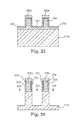
- FIG. 33 illustrates a cross-sectional view of another embodiment of the substrate, the doped semiconductor lines, the spacers, the STI passivation material, the STI fill material, and the conductive cladding after planarization.
- FIG. 34 illustrates a cross-sectional view of another embodiment of the substrate, the doped semiconductor lines, the spacers, the STI passivation material, the STI fill material, and the conductive cladding after planarization.
- FIG. 35 illustrates a cross-sectional view of one embodiment of the substrate, the doped semiconductor lines, the hard mask material layer, and a gas immersion laser doped material layer.
- FIG. 36 illustrates a cross-sectional view of one embodiment of the substrate, the doped semiconductor lines, the hard mask material layer, and conductive cladding after etching the gas immersion laser doped material layer and the substrate.
- FIG. 37 illustrates a cross-sectional view of one embodiment of the substrate, the doped semiconductor lines, the hard mask material layer, the conductive cladding, STI passivation material, and STI fill material.
- FIG. 38 illustrates a cross-sectional view of one embodiment of the substrate, the doped semiconductor lines, the conductive cladding, the STI passivation material, and the STI fill material after planarization.
- FIG. 1 is a block diagram illustrating one embodiment of a system 90 .
- System 90 includes a host 92 and a memory device 100 .
- Host 92 is communicatively coupled to memory device 100 through communication link 94 .
- Host 92 includes a computer (e.g., desktop, laptop, handheld), portable electronic device (e.g., cellular phone, personal digital assistant (PDA), MP3 player, video player), or any other suitable device that uses memory.
- Memory device 100 provides memory for host 92 .
- memory device 100 includes a phase change memory device or other suitable resistive or resistivity changing material memory device.
- FIG. 2A is a diagram illustrating one embodiment of a memory device 100 a .
- memory device 100 a is an integrated circuit or part of an integrated circuit.
- Memory device 100 a includes a write circuit 124 , a controller 120 , a memory array 101 a , and a sense circuit 126 .
- Memory array 101 a includes a plurality of phase change memory cells 104 a - 104 d (collectively referred to as phase change memory cells 104 ), a plurality of bit lines (BLs) 112 a - 112 b (collectively referred to as bit lines 112 ), a plurality of word lines (WLs) 110 a - 110 b (collectively referred to as word lines 110 ), and a plurality of common or ground lines (GLs) 114 a - 114 b (collectively referred to as ground lines 114 ).
- phase change memory cells 104 a - 104 d are arranged in rows and columns.
- ground lines 114 are formed in a semiconductor substrate by doping the semiconductor substrate and forming isolation regions to provide doped lines of semiconductor material.
- the semiconductor substrate is a single crystal silicon substrate and the doped lines are N+ doped silicon lines.
- the doped lines include a conductive cladding that increases the current density for the lines and reduces the overall resistivity of the lines.
- the conductive cladding includes C, TiN, a silicide, a gas immersion laser doped (GILD) material, or another suitable material.
- the doped lines with conductive cladding reduce the voltage drop across the lines and therefore can be used without area consuming stitching to back end of line (BEOL) metallization levels.
- electrically coupled is not meant to mean that the elements must be directly coupled together and intervening elements may be provided between the “electrically coupled” elements.
- Memory array 101 a is electrically coupled to write circuit 124 through signal path 125 , to controller 120 through signal path 121 , and to sense circuit 126 through signal path 127 .
- Controller 120 is electrically coupled to write circuit 124 through signal path 128 and to sense circuit 126 through signal path 130 .
- Each phase change memory cell 104 is electrically coupled to a word line 110 , a bit line 112 , and a common or ground line 114 .
- Phase change memory cell 104 a is electrically coupled to bit line 112 a , word line 110 a , and common or ground line 114 a
- phase change memory cell 104 b is electrically coupled to bit line 112 a , word line 110 b , and common or ground line 114 b .
- Phase change memory cell 104 c is electrically coupled to bit line 112 b , word line 110 a , and common or ground line 114 a
- phase change memory cell 104 d is electrically coupled to bit line 112 b , word line 110 b , and common or ground line 114 b.
- Each phase change memory cell 104 includes a phase change element 106 and a transistor 108 .
- transistor 108 is a field-effect transistor (FET) in the illustrated embodiment, in other embodiments, transistor 108 can be another suitable device such as a bipolar transistor or a 3D transistor structure.
- Phase change memory cell 104 a includes phase change element 106 a and transistor 108 a .
- One side of phase change element 106 a is electrically coupled to bit line 112 a
- the other side of phase change element 106 a is electrically coupled to one side of the source-drain path of transistor 108 a .
- the other side of the source-drain path of transistor 108 a is electrically coupled to common or ground line 114 a .
- the gate of transistor 108 a is electrically coupled to word line 110 a.
- Phase change memory cell 104 b includes phase change element 106 b and transistor 108 b .
- One side of phase change element 106 b is electrically coupled to bit line 112 a
- the other side of phase change element 106 b is electrically coupled to one side of the source-drain path of transistor 108 b .
- the other side of the source-drain path of transistor 108 b is electrically coupled to common or ground line 114 b .
- the gate of transistor 108 b is electrically coupled to word line 110 b.
- Phase change memory cell 104 c includes phase change element 106 c and transistor 108 c .
- One side of phase change element 106 c is electrically coupled to bit line 112 b and the other side of phase change element 106 c is electrically coupled to one side of the source-drain path of transistor 108 c .
- the other side of the source-drain path of transistor 108 c is electrically coupled to common or ground line 114 a .
- the gate of transistor 108 c is electrically coupled to word line 110 a.
- Phase change memory cell 104 d includes phase change element 106 d and transistor 108 d .
- One side of phase change element 106 d is electrically coupled to bit line 112 b and the other side of phase change element 106 d is electrically coupled to one side of the source-drain path of transistor 108 d .
- the other side of the source-drain path of transistor 108 d is electrically coupled to common or ground line 114 b .
- the gate of transistor 108 d is electrically coupled to word line 110 b.
- each phase change element 106 is electrically coupled to a common or ground line 114 and each transistor 108 is electrically coupled to a bit line 112 .
- phase change memory cell 104 a one side of phase change element 106 a is electrically coupled to common or ground line 114 a .
- the other side of phase change element 106 a is electrically coupled to one side of the source-drain path of transistor 108 a .
- the other side of the source-drain path of transistor 108 a is electrically coupled to bit line 112 a.
- Each phase change element 106 comprises a phase change material that may be made up of a variety of materials in accordance with the present invention.
- chalcogenide alloys that contain one or more elements from group VI of the periodic table are useful as such materials.
- the phase change material of phase change element 106 is made up of a chalcogenide compound material, such as GeSbTe, SbTe, GeTe or AgInSbTe.
- the phase change material is chalcogen free, such as GeSb, GaSb, InSb, or GeGaInSb.
- the phase change material is made up of any suitable material including one or more of the elements Ge, Sb, Te, Ga, As, In, Se, and S.
- Each phase change element 106 may be changed from an amorphous state to a crystalline state or from a crystalline state to an amorphous state under the influence of temperature change.
- the amount of crystalline material coexisting with amorphous material in the phase change material of one of the phase change elements 106 a - 106 d thereby defines two or more states for storing data within memory device 100 a .
- a phase change material exhibits significantly higher resistivity than in the crystalline state. Therefore, the two or more states of phase change elements 106 a - 106 d differ in their electrical resistivity.
- the two or more states are two states and a binary system is used, wherein the two states are assigned bit values of “0” and “1”.
- the two or more states are three states and a ternary system is used, wherein the three states are assigned bit values of “0”, “1”, and “2”. In another embodiment, the two or more states are four states that can be assigned multi-bit values, such as “00”, “01”, “10”, and “1”. In other embodiments, the two or more states can be any suitable number of states in the phase change material of a phase change element.
- Controller 120 includes a microprocessor, microcontroller, or other suitable logic circuitry for controlling the operation of memory device 100 a . Controller 120 controls read and write operations of memory device 100 a including the application of control and data signals to memory array 101 a through write circuit 124 and sense circuit 126 .
- write circuit 124 provides voltage pulses through signal path 125 and bit lines 112 to memory cells 104 to program the memory cells. In other embodiments, write circuit 124 provides current pulses through signal path 125 and bit lines 112 to memory cells 104 to program the memory cells.
- Sense circuit 126 reads each of the two or more states of memory cells 104 through bit lines 112 and signal path 127 .
- sense circuit 126 to read the resistance of one of the memory cells 104 , sense circuit 126 provides current that flows through one of the memory cells 104 . Sense circuit 126 then reads the voltage across that one of the memory cells 104 .
- sense circuit 126 provides voltage across one of the memory cells 104 and reads the current that flows through that one of the memory cells 104 .
- write circuit 124 provides voltage across one of the memory cells 104 and sense circuit 126 reads the current that flows through that one of the memory cells 104 .
- write circuit 124 provides current that flows through one of the memory cells 104 and sense circuit 126 reads the voltage across that one of the memory cells 104 .
- phase change memory cell 104 a During a set operation of phase change memory cell 104 a , one or more set current or voltage pulses are selectively enabled by write circuit 124 and sent through bit line 112 a to phase change element 106 a thereby heating phase change element 106 a above its crystallization temperature (but usually below its melting temperature) with word line 110 a selected to activate transistor 108 a . In this way, phase change element 106 a reaches its crystalline state or a partially crystalline and partially amorphous state during this set operation.
- phase change memory cell 104 a During a reset operation of phase change memory cell 104 a , a reset current or voltage pulse is selectively enabled by write circuit 124 and sent through bit line 112 a to phase change element 106 a .
- the reset current or voltage quickly heats phase change element 106 a above its melting temperature.
- phase change element 106 a quickly quench cools into the amorphous state or a partially amorphous and partially crystalline state.
- Phase change memory cells 104 b - 104 d and other phase change memory cells 104 in memory array 101 a are set and reset similarly to phase change memory cell 104 a using a similar current or voltage pulse.
- FIG. 2B is a diagram illustrating another embodiment of a memory device 100 b .
- Memory device 100 b is similar to memory device 100 a previously described and illustrated with reference to FIG. 2A , except that in memory device 100 b memory array 101 a is replaced with memory array 101 b .
- Memory array 101 b is similar to memory array 101 a , except that in memory array 101 b transistors 108 a - 108 d are replaced with diodes 109 a - 109 d.
- word lines 110 are formed in a semiconductor substrate by doping the semiconductor substrate and forming isolation regions to provide doped lines of semiconductor material.
- the semiconductor substrate is a single crystal silicon substrate and the doped lines are N+ doped silicon lines.
- the doped lines include a conductive cladding that increases the current density for the lines and reduces the overall resistivity of the lines.
- the conductive cladding includes C, TiN, a silicide, a gas immersion laser doped (GILD) material, or another suitable material.
- the doped lines with conductive cladding reduce the voltage drop across the lines and therefore can be used without area consuming stitching to back end of line (BEOL) metallization levels.
- phase change memory cell 104 is electrically coupled to a word line 110 and a bit line 112 .
- Phase change memory cell 104 a is electrically coupled to bit line 112 a and word line 110 a
- phase change memory cell 104 b is electrically coupled to bit line 112 a and word line 110 b
- Phase change memory cell 104 c is electrically coupled to bit line 112 b and word line 110 a
- phase change memory cell 104 d is electrically coupled to bit line 112 b and word line 110 b.
- Each phase change memory cell 104 includes a phase change element 106 and a diode 109 .
- the polarity of diodes 109 is reversed.
- Phase change memory cell 104 a includes phase change element 106 a and diode 109 a .
- One side of phase change element 106 a is electrically coupled to bit line 112 a
- the other side of phase change element 106 a is electrically coupled to one side of diode 109 a
- the other side of diode 109 a is electrically coupled to word line 110 a.
- Phase change memory cell 104 b includes phase change element 106 b and diode 109 b .
- One side of phase change element 106 b is electrically coupled to bit line 112 a
- the other side of phase change element 106 b is electrically coupled to one side of diode 109 b .
- the other side of diode 109 b is electrically coupled to word line 110 b.
- Phase change memory cell 104 c includes phase change element 106 c and diode 109 c .
- One side of phase change element 106 c is electrically coupled to bit line 112 b and the other side of phase change element 106 c is electrically coupled to one side of diode 109 c .
- the other side of diode 109 c is electrically coupled to word line 110 a.
- Phase change memory cell 104 d includes phase change element 106 d and diode 109 d .
- One side of phase change element 106 d is electrically coupled to bit line 112 b and the other side of phase change element 106 d is electrically coupled to one side of diode 109 d .
- the other side of diode 109 d is electrically coupled to word line 110 b.
- each phase change element 106 is electrically coupled to a word line 110 and each diode 109 is electrically coupled to a bit line 112 .
- phase change memory cell 104 a one side of phase change element 106 a is electrically coupled to word line 110 a .
- the other side of phase change element 106 a is electrically coupled to one side of diode 109 a .
- the other side of diode 109 a is electrically coupled to bit line 112 a .
- Memory device 100 b operates similarly to memory device 100 a previously described and illustrated with reference to FIG. 2A .
- Embodiments of the present invention relate to new memory technologies based on Si technology, especially to the reduction of the wire resistance of doped Si wires used in the memory array for cell selection.
- a high performance select array device is used to switch high select currents and/or high select voltages. In this case, it is desirable to reduce the line resistances of the select device to a minimal value.
- the select device is typically a select diode, a bipolar transistor, or a field effect transistor (FET) like transistor.
- memory arrays use heavily doped Si wires for cell device selection. These wires are used to carry the programming or read current. These wires can also serve as potential mesh (e.g. ground). The current densities, however, are limited and the resistance of these wires is often too high leading to a harmful voltage drop across the line and undesired power losses along the line resistances.
- the manufacturing of the conductive cladding lines can either be chronologically separated from the select device manufacturing process or be included within the select device manufacturing steps.
- the incorporation of fabrication of the conductive cladding lines can be different for diode based select devices, bipolar transistor select devices, or FET like select devices.
- the conductive cladding lines can directly contact the memory cell.
- the select device is indirectly coupled to the cladding lines via the memory cell.
- FIG. 3A illustrates a perspective view of one embodiment of a doped semiconductor line 202 including conductive cladding 203 .
- doped semiconductor line 202 is an N+ doped Si line formed from a Si substrate.
- Conductive cladding 203 laterally surrounds doped semiconductor line 202 .
- Conductive cladding 203 includes C, TiN, a silicide, a GILD material, or another suitable conductive material.
- conductive cladding 203 contacts one vertical sidewall of doped semiconductor line 202 and not the other vertical sidewall of doped semiconductor line 202 .
- a diode including an N ⁇ doped Si region 206 and a P+ doped Si region 208 contacts doped semiconductor line 202 .
- a silicide contact 210 contacts P+ doped Si region 208 .
- silicide contact 210 includes CoSi 2 , TiSi 2 , NiSi, or another suitable silicide.
- word lines 110 are similar to doped semiconductor line 202 with conductive cladding 203 and diodes 109 are similar to the diode provided by N ⁇ doped Si region 206 and P+ doped Si region 208 .
- ground lines 114 are similar to doped semiconductor line 202 with conductive cladding 203 and a source or drain region of each transistor 108 contacts a doped semiconductor line 202 .
- FIG. 3B illustrates a cross-sectional view of one embodiment of doped semiconductor lines 202 including conductive cladding 203 .
- Doped semiconductor lines 202 are formed in substrate 212 .
- Isolation regions 216 such as shallow trench isolation (STI) or other suitable isolation, electrically isolates adjacent doped semiconductor lines 202 including conductive cladding 203 from each other.
- the bottom and one sidewall of conductive cladding 203 contacts doped semiconductor line 202 .
- substrate 212 is properly doped. Both, STI isolation and proper doping is used to suppress leakage currents between neighboring lines 202 .
- FIG. 4 illustrates a perspective view of another embodiment of a doped semiconductor line 202 including conductive cladding 204 .
- This embodiment is similar to the embodiment previously described and illustrated with reference to FIG. 3A , except that in this embodiment conductive cladding 203 is replaced by conductive cladding 204 .
- Conductive cladding 204 laterally encloses a portion of doped semiconductor line 202 .
- the bottom and one sidewall of conductive cladding 204 contacts doped semiconductor line 202 .
- conductive cladding 204 contacts one vertical sidewall of doped semiconductor line 202 and not the other vertical sidewall of doped semiconductor line 202 .
- FIG. 5 illustrates a perspective view of another embodiment of a doped semiconductor line 202 including conductive cladding 205 .
- This embodiment is similar to the embodiment previously described and illustrated with reference to FIG. 3A , except that in this embodiment conductive cladding 203 is replaced by conductive cladding 205 .
- Conductive cladding 205 contacts a portion of the vertical sidewalls of doped semiconductor line 202 and extends into a central portion of doped semiconductor line 202 .
- the bottom of conductive cladding 205 contacts doped semiconductor line 202 .
- conductive cladding 205 contacts one vertical sidewall of doped semiconductor line 202 and not the other vertical sidewall of doped semiconductor line 202 .
- doped semiconductor lines 202 including conductive cladding 205 are buried in or embraced by a properly doped semiconductor to avoid inter-wiring leakage via the substrate.
- the doped region can consist of similar doping as silicon wire.
- FIGS. 6-38 illustrate embodiments for fabricating doped semiconductor lines 202 including conductive cladding, such as conductive cladding 203 , 204 , or 205 . While the illustrated embodiments are focused on using a bulk Si wafer, the embodiments can also be adapted for using silicon on insulator (SOI) wafers or other suitable substrates.
- FIGS. 6-13 illustrate embodiments for fabricating doped semiconductor lines 202 including conductive cladding 203 as previously described and illustrated with reference to FIG. 3A .
- FIG. 6 illustrates a cross-sectional view of one embodiment of a doped semiconductor substrate.
- a substrate is doped to provide a doped region 202 a and an undoped region 212 a .
- a single crystal Si substrate is doped to provide an N+ doped Si region 202 a and an undoped Si region 212 a.
- FIG. 7 illustrates a cross-sectional view of one embodiment of the doped semiconductor substrate and a hard mask material layer 220 a .
- a hard mask material such as SiN or another suitable material is deposited over doped region 202 a to provide a hard mask material layer.
- the hard mask material layer is deposited using chemical vapor deposition (CVD), high density plasma-chemical vapor deposition (HDP-CVD), atomic layer deposition (ALD), metal organic chemical vapor deposition (MOCVD), physical vapor deposition (PVD), jet vapor deposition (JVP), or other suitable deposition technique.
- CVD chemical vapor deposition
- HDP-CVD high density plasma-chemical vapor deposition
- ALD atomic layer deposition
- MOCVD metal organic chemical vapor deposition
- PVD physical vapor deposition
- JVP jet vapor deposition
- hard mask material layer 220 a is then patterned using a photolithography process or another suitable process and etched to expose portions of doped region 202 a to provide hard mask material layer 220 a .
- hard mask material layer 220 a includes lines of hard mask material.
- FIG. 8 illustrates a cross-sectional view of one embodiment of substrate 212 a , doped semiconductor lines 202 , and hard mask material layer 220 a after etching doped region 202 a .
- the exposed portions of doped region 202 a are etched to provide openings 221 .
- openings 221 are trenches.
- the exposed portions of doped region 202 a are etched to provide openings 221 leaving semiconductor materials 202 over substrate 212 a .
- portions of substrate 212 a below openings 221 are also etched.
- Substrate 212 a is then doped to minimize leakage current between doped semiconductor lines 202 .
- FIG. 9 illustrates a cross-sectional view of one embodiment of substrate 212 a , doped semiconductor lines 202 , hard mask material layer 220 a , a cladding material layer 222 a , and a dielectric material layer 224 a .
- a cladding material such as C, TiN, or another suitable conductive material is deposited over exposed portions of hard mask material layer 220 a , doped semiconductor lines 202 , and substrate 212 a to provide cladding material layer 222 a .
- Cladding material layer 222 a is deposited using CVD, HDP-CVD, ALD, MOCVD, PVD, JVP, or other suitable deposition technique.
- a dielectric material such as SiO 2 , SiN, non-conducting amorphous carbon, or another suitable dielectric material is deposited over cladding material layer 222 a to provide dielectric material layer 224 a .
- Dielectric material layer 224 a is deposited using CVD, HDP-CVD, ALD, MOCVD, PVD, JVP, or other suitable deposition technique.
- FIG. 10A illustrates a cross-sectional view of one embodiment of substrate 212 a , doped semiconductor lines 202 , hard mask material layer 220 a , cladding material layer 222 b , and dielectric material layer 224 b after etching dielectric material layer 224 a and cladding material layer 222 a .
- the portions of dielectric material layer 224 a and cladding material layer 222 a at the bottom of openings 221 are selectively etched to expose portions of doped semiconductor lines 202 and to provide dielectric material layer 224 b and cladding material layer 222 b.
- FIG. 10B illustrates a cross-sectional view of another embodiment of substrate 212 a , doped semiconductor lines 202 , hard mask material layer 220 a , cladding material layer 222 c , and dielectric material layer 224 c after etching dielectric material layer 224 a and cladding material layer 222 a .
- dielectric material layer 224 a and cladding material layer 222 a are spacer etched to expose hard mask material layer 220 a and portions of doped semiconductor lines 202 to provide dielectric material layer 224 c and cladding material layer 222 c . While the following FIGS.
- dielectric material layer 224 c and cladding material layer 222 c include dielectric material layer 224 c and cladding material layer 222 c , dielectric material layer 224 b and cladding material layer 222 b illustrated with reference to FIG. 10A can be used in place of dielectric material layer 224 c and cladding material layer 222 c.
- FIG. 11 illustrates a cross-sectional view of one embodiment of substrate 212 b , doped semiconductor lines 202 , hard mask material layer 220 a , cladding material layer 222 c , and dielectric material layer 224 c after etching portions of doped semiconductor lines 202 and substrate 212 a .
- the exposed portions of doped semiconductor lines 202 and optionally the underlying portions of substrate 212 a are etched to provide openings 228 and substrate 212 b.
- FIG. 12 illustrates a cross-sectional view of one embodiment of substrate 212 b , doped semiconductor lines 202 , hard mask material layer 220 a , cladding material layer 222 c , dielectric material layer 224 c , STI passivation material 230 a , and STI fill material 216 a .
- Exposed portions of dielectric material layer 224 c and substrate 212 b are subjected to an STI passivation process to oxidize the exposed surfaces of dielectric material layer 224 c and substrate 212 b to provide STI passivation material 230 a .
- a portion of cladding material layer 222 c as indicated at 223 may also be oxidized during the STI passivation process.
- STI fill material such as SiO 2 , fluorinated silica glass (FSG), boron-phosphorous silicate glass (BPSG), boron-silicate glass (BSG), or other suitable dielectric material is deposited over exposed portions of hard mask material layer 220 a , cladding material layer 222 c , dielectric material layer 224 c , and STI passivation material 230 a to provide STI fill material 216 a .
- STI fill material 216 a is deposited using CVD, HDP-CVD, ALD, MOCVD, PVD, JVP, spin-on, or other suitable deposition technique.
- FIG. 13 illustrates a cross-sectional view of one embodiment of substrate 212 b , doped semiconductor lines 202 , conductive cladding 203 , dielectric material 224 , STI passivation material 230 b , and STI fill material 216 after planarization.
- STI fill material 216 a , hard mask material layer 220 a , cladding material layer 222 c , dielectric material layer 224 c , and STI passivation material 230 a are planarized to expose doped semiconductor lines 202 to provide conductive cladding 203 , dielectric material 224 , STI passivation material 230 b , and STI fill material 216 .
- STI fill material 216 a , hard mask material layer 220 a , cladding material layer 222 c , dielectric material layer 224 c , and STI passivation material 230 a are planarized using chemical mechanical planarization (CMP) or another suitable planarization technique to provide doped semiconductor lines 202 including conductive cladding 203 as previously described and illustrated with reference to FIG. 3A .
- CMP chemical mechanical planarization
- FIGS. 14-19 illustrate embodiments for fabricating doped semiconductor lines 202 including conductive cladding 203 as previously described and illustrated with reference to FIG. 3A .
- the fabrication process begins as previously described and illustrated with reference to FIGS. 6 and 7 .
- FIG. 14 illustrates a cross-sectional view of one embodiment of substrate 212 c , doped semiconductor lines 202 b , and hard mask material layer 220 a after etching doped region 202 a and substrate 212 a .
- the exposed portions of doped region 202 a and the underlying portions of substrate 212 a are etched to provide openings 232 , doped semiconductor lines 202 b , and substrate 212 c .
- openings 232 are trenches.
- FIG. 15 illustrates a cross-sectional view of one embodiment of substrate 212 c , doped semiconductor lines 202 b , hard mask material layer 220 a , STI passivation material 230 a , and STI fill material 216 b . Exposed portions of hard mask material layer 220 a , doped semiconductor lines 202 b , and substrate 212 c are subjected to an STI passivation process to oxidize the exposed surfaces of hard mask material layer 220 a , doped semiconductor lines 202 b , and substrate 212 c to provide STI passivation material.
- An STI fill material such as SiO 2 , FSG, BPSG, BSG, or other suitable dielectric material is deposited over the STI passivation material.
- the STI fill material is deposited using CVD, HDP-CVD, ALD, MOCVD, PVD, JVP, spin-on, or other suitable deposition technique.
- the STI fill material and the STI passivation material is then planarized to expose hard mask material layer 220 a to provide STI passivation material 230 a and STI fill material 216 b .
- the STI fill material and the STI passivation material are planarized using CMP or another suitable planarization technique.
- FIG. 16 illustrates a cross-sectional view of one embodiment of substrate 212 c , doped semiconductor lines 202 b , hard mask material layer 220 a , STI passivation material 230 b , and STI fill material 216 after etching STI passivation material 230 a and STI fill material 216 b .
- STI passivation material 230 a and STI fill material 216 b are etched using CMP dishing, an HF dip, a selective etch, or another suitable technique to expose the sidewalls of hard mask material layer 220 a to provide STI passivation material 230 b and STI fill material 216 .
- FIG. 17 illustrates a cross-sectional view of one embodiment of substrate 212 c , doped semiconductor lines 202 b , hard mask material layer 220 b , STI passivation material 230 b , and STI fill material 216 after etching hard mask material layer 220 a .
- Hard mask material layer 220 a is etched using a recess etch or another suitable technique to expose portions of doped semiconductor lines 202 b.
- FIG. 18 illustrates a cross-sectional view of one embodiment of substrate 212 d , doped semiconductor lines 202 , hard mask material layer 220 b , STI passivation material 230 b , and STI fill material 216 after etching doped semiconductor lines 202 b .
- the exposed portions of doped semiconductor lines 202 b and optionally the underlying portions of substrate 212 c are selectively etched to a desired depth to provide openings 234 , doped semiconductor lines 202 , and optionally substrate 212 d.
- FIG. 19 illustrates a cross-sectional view of one embodiment of substrate 212 d , doped semiconductor lines 202 , hard mask material layer 220 b , STI passivation material 230 b , STI fill material 216 , and a cladding material 222 d .
- a cladding material such as C, TiN, or another suitable conductive material is deposited over exposed portions of hard mask material layer 220 b , doped semiconductor lines 202 , STI passivation material 230 b , and STI fill material 216 to provide cladding material 222 d .
- Cladding material 222 d is deposited using CVD, HDP-CVD, ALD, MOCVD, PVD, JVP, or other suitable deposition technique.
- Cladding material 222 d and hard mask material layer 220 b is then planarized to expose doped semiconductor lines 202 and STI fill material 216 to provide doped semiconductor line 202 including conductive cladding 203 as previously described and illustrated with reference to FIG. 3A .
- Cladding material 222 d and hard mask material layer 220 b are planarized using CMP or another suitable planarization technique.
- FIGS. 20A-24 illustrate embodiments for fabricating doped semiconductor lines 202 including conductive cladding 205 as previously described and illustrated with reference to FIG. 5 .
- the fabrication process begins as previously described and illustrated with reference to FIGS. 6 , 7 , 14 , and 15 .
- FIG. 20A illustrates a cross-sectional view of one embodiment of substrate 212 c , doped semiconductor lines 202 b , STI passivation material 230 c , and STI fill material 216 c after etching.
- STI passivation material 230 a and STI fill material 216 b are etched to a desired depth to provide openings 236 a , STI passivation material 230 c , and STI fill material 216 c .
- openings 236 a expose a portion of the sidewalls of doped semiconductor lines 202 b .
- Hard mask material layer 220 a is removed to expose the tops of doped semiconductor lines 202 b.
- FIG. 20B illustrates a cross-sectional view of another embodiment of substrate 212 c , doped semiconductor lines 202 b , STI passivation material 230 d , and STI fill material 216 d after etching.
- STI passivation material 230 a and STI fill material 216 b are etched to a desired depth to provide openings 236 b , STI passivation material 230 d , and STI fill material 216 d .
- openings 236 b expose the sidewalls of doped semiconductor lines 202 b .
- Hard mask material layer 220 a is removed to expose the tops of doped semiconductor lines 202 b.
- FIG. 20C illustrates a cross-sectional view of another embodiment of substrate 212 c , doped semiconductor lines 202 b , STI passivation material 230 e , and STI fill material 216 e after etching.
- STI passivation material 230 a and STI fill material 216 b are etched to a desired depth to provide openings 236 c , STI passivation material 230 e , and STI fill material 216 e .
- openings 236 c expose the sidewalls of doped semiconductor lines 202 b and portions of the sidewalls of substrate 212 c .
- Hard mask material layer 220 a is removed to expose the tops of doped semiconductor lines 202 b.
- the depth of openings 236 a ( FIG. 20A ), 236 b ( FIG. 20B ), and 236 c ( FIG. 20C ) are selected based on process and performance optimization and/or based on the doping profile of doped semiconductor lines 202 .
- Direct contact of a cladding line with substrate 212 c may result in an undesired leakage current between neighboring doped semiconductor lines 202 b . Therefore, substrate 212 c is properly doped to minimize leakage currents.
- the cladding lines 222 d may be surrounded by n-doped regions.
- FIGS. 21 and 22 include STI passivation material 230 c and STI fill material 216 c as illustrated with reference to FIG. 20A
- STI passivation material 230 d and STI fill material 216 d as illustrated with reference to FIG. 20B or STI passivation material 230 e and STI fill material 216 e as illustrated with reference to FIG. 20C can be used in place of STI passivation material 230 c and STI fill material 216 c.
- FIG. 21 illustrates a cross-sectional view of one embodiment of substrate 212 c , doped semiconductor lines 202 b , STI passivation material 230 c , STI fill material 216 c , and a spacer material layer 238 a .
- a spacer material such as SiN or another suitable spacer material is deposited over exposed portions of doped semiconductor lines 202 b , STI passivation material 230 c , and STI fill material 216 c to provide spacer material layer 238 a .
- Spacer material layer 238 a is deposited using CVD, HDP-CVD, ALD, MOCVD, PVD, JVP, or other suitable deposition technique.
- FIG. 22 illustrates a cross-sectional view of one embodiment of substrate 212 c , doped semiconductor lines 202 b , STI passivation material 230 c , STI fill material 216 c , and spacer material layer 238 b after etching spacer material layer 238 a .
- Spacer material layer 238 a is etched to expose portions of STI fill material 216 c and to provide spacer material layer 238 b.
- FIG. 23 illustrates a cross-sectional view of one embodiment of substrate 212 e , doped semiconductor lines 202 c , STI passivation material 230 f , STI fill material 216 f , and spacer material layer 238 b after etching STI passivation material 230 c , STI fill material 216 c , doped semiconductor lines 202 b , and optionally substrate 212 c .
- STI passivation material 230 c and STI fill material 216 c are etched to expose portions of doped semiconductor lines 202 b to provide STI passivation material 230 f and STI fill material 216 f .
- the exposed portions of doped semiconductor lines 202 b and the optionally adjacent portions of substrate 212 c are then selectively etched to provide openings 240 and doped semiconductor lines 202 c and optionally substrate 212 e.
- FIG. 24 illustrates a cross-sectional view of one embodiment of substrate 212 e , doped semiconductor lines 202 c , STI passivation material 230 f , STI fill material 216 f , spacer material layer 238 b , and a cladding material 222 e .
- a cladding material such as C, TiN, or another suitable conductive material is deposited over exposed portions of spacer material layer 238 b , doped semiconductor lines 202 c , STI passivation material 230 f , STI fill material 216 f , and substrate 212 e to provide cladding material 222 e .
- Cladding material 222 e is deposited using CVD, HDP-CVD, ALD, MOCVD, PVD, JVP, or other suitable deposition technique.
- Cladding material 222 e is etched to expose STI fill material 216 f .
- the fabrication process then continues as previously described and illustrated with reference to FIGS. 12 and 13 to provide doped semiconductor lines 202 c including conductive cladding similar to doped semiconductor line 202 including conductive cladding 205 previously described and illustrated with reference to FIG. 5 .
- FIGS. 25-31 illustrate embodiments for fabricating doped semiconductor lines 202 including conductive cladding 203 as previously described and illustrated with reference to FIG. 3A .
- the fabrication process begins as previously described and illustrated with reference to FIGS. 6 , 7 , and 14 .
- FIG. 25 illustrates a cross-sectional view of one embodiment of substrate 212 c , doped semiconductor lines 202 , hard mask material layer 220 a , a sacrificial material layer 242 a , and a spacer material layer 244 a .
- a sacrificial material such as SiO 2 or another suitable material is deposited over exposed portions of hard mask material layer 220 a , doped semiconductor lines 202 , and substrate 212 c to provide sacrificial material layer 242 a .
- Sacrificial material layer 242 a is deposited using CVD, HDP-CVD, ALD, MOCVD, PVD, JVP, or other suitable deposition technique.
- a spacer material such as SiN or another suitable spacer material is deposited over sacrificial material layer 242 a to provide spacer material layer 244 a .
- Spacer material layer 244 a is deposited using CVD, HDP-CVD, ALD, MOCVD, PVD, JVP, or other suitable deposition technique.
- FIG. 26 illustrates a cross-sectional view of one embodiment of substrate 212 c , doped semiconductor lines 202 , hard mask material layer 220 a , sacrificial material layer 242 a , and spacers 244 b after etching spacer material layer 244 a .
- Spacer material layer 244 a is spacer etched to expose portions of sacrificial material layer 242 a to provide spacers 244 b.
- FIG. 27 illustrates a cross-sectional view of one embodiment of substrate 212 f , doped semiconductor lines 202 , hard mask material layer 220 a , sacrificial material layer 242 b , and spacers 244 b after etching sacrificial material layer 242 a and substrate 212 c .
- the exposed horizontal portions of sacrificial material layer 242 a are etched to expose hard mask material layer 220 a and substrate 212 c to provide sacrificial material layer 242 b .
- the exposed portions of substrate 212 c are optionally etched to provide openings 246 and substrate 212 f.
- FIG. 28 illustrates a cross-sectional view of one embodiment of substrate 212 f , doped semiconductor lines 202 , hard mask material layer 220 a , sacrificial material layer 242 b , spacers 244 b , STI passivation material 230 g , and STI fill material 216 g .
- Exposed portions of sacrificial material layer 242 b , spacers 244 b , and substrate 212 f are subjected to an STI passivation process to oxidize the exposed surfaces of sacrificial material layer 242 b , spacers 244 b , and substrate 212 f to provide STI passivation material.
- An STI fill material such as SiO 2 , FSG, BPSG, BSG, or other suitable dielectric material is deposited over the STI passivation material.
- the STI fill material is deposited using CVD, HDP-CVD, ALD, MOCVD, PVD, JVP, spin-on, or other suitable deposition technique.
- the STI fill material and the STI passivation material is then planarized to expose hard mask material layer 220 a to provide STI passivation material 230 g and STI fill material 216 g .
- the STI fill material and the STI passivation material are planarized using CMP or another suitable planarization technique.
- FIG. 29 illustrates a cross-sectional view of one embodiment of substrate 212 f , doped semiconductor lines 202 , hard mask material layer 220 a , sacrificial material layer 242 c , spacers 244 b , STI passivation material 230 g , and STI fill material 216 g after etching sacrificial material layer 242 b .
- Sacrificial material layer 242 b is etched to provide openings 248 having a desired depth and to provide sacrificial material layer 242 c.
- FIG. 30 illustrates a cross-sectional view of one embodiment of substrate 212 f , doped semiconductor lines 202 , hard mask material layer 220 a , sacrificial material layer 242 c , spacers 244 b , STI passivation material 230 g , STI fill material 216 g , and a cladding material 222 f .
- a cladding material such as C, TiN, or another suitable conductive material is deposited over exposed portions of hard mask material layer 220 a , doped semiconductor lines 202 , sacrificial material layer 242 c , STI passivation material 230 g , STI fill material 216 g , and substrate 212 f to provide cladding material 222 f .
- Cladding material 222 f is deposited using CVD, HDP-CVD, ALD, MOCVD, PVD, JVP, or other suitable deposition technique.
- FIG. 31 illustrates a cross-sectional view of one embodiment of substrate 212 f , doped semiconductor lines 202 , sacrificial material layer 242 c , spacers 244 c , STI passivation material 230 h , STI fill material 216 , and conductive cladding 203 after planarization.
- Cladding material 222 f , hard mask material layer 220 a , spacers 244 b , STI passivation material 230 g , and STI fill material 216 g are planarized to expose doped semiconductor lines 202 to provide conductive cladding 203 , spacers 244 c , STI passivation material 230 h , and STI fill material 216 .
- Cladding material 222 f , hard mask material layer 220 a , spacers 244 b , STI passivation material 230 g , and STI fill material 216 g are planarized using CMP or another suitable planarization technique to provide doped semiconductor line 202 including conductive cladding 203 as previously described and illustrated with reference to FIG. 3A .
- FIG. 32 illustrates a cross-sectional view of another embodiment of substrate 212 f , doped semiconductor lines 202 , spacers 244 c , STI passivation material 230 h , STI fill material 216 , and conductive cladding 222 g after planarization.
- This embodiment is similar to the embodiment previously described and illustrated with reference to FIG. 31 , except that in this embodiment sacrificial material layer 242 b is completely removed and replaced by conductive cladding 222 g .
- Substrate 212 f is properly doped to minimize leakage currents between doped semiconductor lines 202 .
- FIG. 33 illustrates a cross-sectional view of another embodiment of substrate 212 g , doped semiconductor lines 202 , spacers 244 d , STI passivation material 230 h , STI fill material 216 , and conductive cladding 222 h after planarization.
- This embodiment is similar to the embodiment previously described and illustrated with reference to FIG. 31 , except that in this embodiment conductive cladding 222 h and spacers 244 d both have the same height as doped semiconductor lines 202 .
- the sacrificial material layer is completely removed and replaced by conductive cladding 222 h .
- Substrate 212 g is properly doped to minimize leakage currents between doped semiconductor lines 202 .
- FIG. 34 illustrates a cross-sectional view of another embodiment of substrate 212 g , doped semiconductor lines 202 , spacers 244 e , STI passivation material 230 h , STI fill material 216 , and conductive cladding 222 i after planarization.
- This embodiment is similar to the embodiment previously described and illustrated with reference to FIG. 33 , except that this embodiment includes an additional doped region 250 .
- doped semiconductor line 202 includes an N+ doped lower region and an N ⁇ doped upper region. The N ⁇ doped upper region contacts a P doped region 250 .
- Doped semiconductor line 202 and P doped region 250 are both etched from the substrate. P doped region 250 is then etched to provide individual diodes contacting doped semiconductor line 202 including conductive cladding 222 i.
- FIGS. 35-38 illustrate embodiments for fabricating doped semiconductor lines 202 including conductive cladding 203 as previously described and illustrated with reference to FIG. 3A .
- the fabrication process begins as previously described and illustrated with reference to FIGS. 6-8 .
- FIG. 35 illustrates a cross-sectional view of one embodiment of substrate 212 a , doped semiconductor lines 202 , hard mask material layer 220 a , and a gas immersion laser doped (GILD) material layer 252 .
- the exposed portions of doped semiconductor lines 202 and optionally substrate 212 a are subjected to a gas immersion laser doping process.
- BCl 3 is used as the dopant in the GILD process to provide GILD material layer 252 .
- FIG. 36 illustrates a cross-sectional view of one embodiment of substrate 212 h , doped semiconductor lines 202 , hard mask material layer 220 a , and conductive cladding 203 after etching GILD material layer 252 and substrate 212 a .
- the horizontal portions of GILD material layer 252 are etched to expose portions of doped semiconductor lines 202 and to provide conductive cladding 203 .
- the exposed portions of doped semiconductor lines 202 and the underlying portions of substrate 212 a are then etched to provide openings 254 and to provide substrate 212 h.
- FIG. 37 illustrates a cross-sectional view of one embodiment of substrate 212 h , doped semiconductor lines 202 , hard mask material layer 220 a , conductive cladding 203 , STI passivation material 230 i , and STI fill material 216 h .
- Exposed portions of hard mask material layer 220 a , conductive cladding 203 , and substrate 212 h are subjected to an STI passivation process to oxidize the exposed surfaces of hard mask material layer 220 a , conductive cladding 203 , and substrate 212 h to provide STI passivation material 230 i.
- STI fill material such as SiO 2 , FSG, BPSG, BSG, or other suitable dielectric material is deposited over exposed portions of hard mask material layer 220 a and STI passivation material 230 i to provide STI fill material 216 h .
- STI fill material 216 h is deposited using CVD, HDP-CVD, ALD, MOCVD, PVD, JVP, spin-on, or other suitable deposition technique.
- the STI regions are formed before the gas immersion laser doping process is performed.
- FIG. 38 illustrates a cross-sectional view of one embodiment of substrate 212 h , doped semiconductor lines 202 , conductive cladding 203 , STI passivation material 230 j , and STI fill material 216 after planarization.
- STI fill material 216 h , hard mask material layer 220 a , and STI passivation material 230 i are planarized to expose doped semiconductor lines 202 to provide STI passivation material 230 j and STI fill material 216 .
- STI fill material 216 h , hard mask material layer 220 a , and STI passivation material 230 i are planarized using CMP or another suitable planarization technique to provide doped semiconductor lines 202 including conductive cladding 203 as previously described and illustrated with reference to FIG. 3A .
- the GILD process followed by a dielectric material fill can be used in place of the deposition of cladding material 222 d previously described and illustrated with reference to FIG. 19 .
- the GILD process followed by a dielectric material fill can be used in place of the deposition of cladding material 222 f previously described and illustrated with reference to FIG. 30 .
- Embodiments provide doped semiconductor lines including conductive cladding.
- the lines can be used as memory cell select lines within an array of memory cells.
- the lines increase the current densities that can be achieved compared to unclad lines and reduce cross-talk between diode select devices in a memory array.
- the lines have a low resistivity such that the lines can be used without area consuming stitching to back end of line (BEOL) metallization levels.
- BEOL back end of line
- phase change memory elements While the specific embodiments described herein substantially focused on using phase change memory elements, the present invention is applicable to any suitable type of resistive or resistivity changing memory elements. In addition, the embodiments are applicable to any suitable integrated circuit in which conductive lines contacting active devices, such as diodes or transistors, are used.
Landscapes
- Engineering & Computer Science (AREA)
- Physics & Mathematics (AREA)
- Condensed Matter Physics & Semiconductors (AREA)
- General Physics & Mathematics (AREA)
- Manufacturing & Machinery (AREA)
- Computer Hardware Design (AREA)
- Microelectronics & Electronic Packaging (AREA)
- Power Engineering (AREA)
- Semiconductor Memories (AREA)
- Internal Circuitry In Semiconductor Integrated Circuit Devices (AREA)
Abstract
Description
-
- The conductive cladding allows significant high current densities that are important to operate novel memory cell concepts at reduced dimensions.
- The conductive cladding results in a low voltage drop across the line, thus resulting also in reduced power consumption and reduced cross talk effects.
- In combination with diode like cross point select devices, a viable realization is possible.
- The conductive cladding leads to a reduction of diode cross talk.
- The proposed concept is applicable for conventional Si wafer substrates and silicon on insulator (SOI) wafers.
- A low resistive connection is obtained without area consuming stitching to BEOL levels.
Claims (25)
Priority Applications (5)
| Application Number | Priority Date | Filing Date | Title |
|---|---|---|---|
| US11/931,449 US8084759B2 (en) | 2007-10-31 | 2007-10-31 | Integrated circuit including doped semiconductor line having conductive cladding |
| US12/206,439 US8254166B2 (en) | 2007-10-31 | 2008-09-08 | Integrated circuit including doped semiconductor line having conductive cladding |
| DE102008051746A DE102008051746A1 (en) | 2007-10-31 | 2008-10-15 | Integrated circuit with doped semiconductor line with conductive cladding |
| JP2008278509A JP2009111391A (en) | 2007-10-31 | 2008-10-29 | Integrated circuit including doped semiconductor line having conductive cladding |
| CNA2008101752170A CN101447500A (en) | 2007-10-31 | 2008-10-30 | Integrated circuit including doped semiconductor line having conductive cladding |
Applications Claiming Priority (1)
| Application Number | Priority Date | Filing Date | Title |
|---|---|---|---|
| US11/931,449 US8084759B2 (en) | 2007-10-31 | 2007-10-31 | Integrated circuit including doped semiconductor line having conductive cladding |
Related Child Applications (1)
| Application Number | Title | Priority Date | Filing Date |
|---|---|---|---|
| US12/206,439 Continuation US8254166B2 (en) | 2007-10-31 | 2008-09-08 | Integrated circuit including doped semiconductor line having conductive cladding |
Publications (2)
| Publication Number | Publication Date |
|---|---|
| US20090108248A1 US20090108248A1 (en) | 2009-04-30 |
| US8084759B2 true US8084759B2 (en) | 2011-12-27 |
Family
ID=40581656
Family Applications (1)
| Application Number | Title | Priority Date | Filing Date |
|---|---|---|---|
| US11/931,449 Expired - Fee Related US8084759B2 (en) | 2007-10-31 | 2007-10-31 | Integrated circuit including doped semiconductor line having conductive cladding |
Country Status (4)
| Country | Link |
|---|---|
| US (1) | US8084759B2 (en) |
| JP (1) | JP2009111391A (en) |
| CN (1) | CN101447500A (en) |
| DE (1) | DE102008051746A1 (en) |
Cited By (1)
| Publication number | Priority date | Publication date | Assignee | Title |
|---|---|---|---|---|
| US20100061140A1 (en) * | 2007-10-31 | 2010-03-11 | Qimonda Ag | Integrated circuit including doped semiconductor line having conductive cladding |
Families Citing this family (5)
| Publication number | Priority date | Publication date | Assignee | Title |
|---|---|---|---|---|
| US7759770B2 (en) * | 2008-06-23 | 2010-07-20 | Qimonda Ag | Integrated circuit including memory element with high speed low current phase change material |
| US8377813B2 (en) * | 2010-08-27 | 2013-02-19 | Rexchip Electronics Corporation | Split word line fabrication process |
| US8728945B2 (en) * | 2010-11-03 | 2014-05-20 | Texas Instruments Incorporated | Method for patterning sublithographic features |
| US11437283B2 (en) * | 2019-03-15 | 2022-09-06 | Intel Corporation | Backside contacts for semiconductor devices |
| CN113540095B (en) * | 2021-07-19 | 2023-10-24 | 长鑫存储技术有限公司 | Semiconductor structure and manufacturing method thereof |
Citations (10)
| Publication number | Priority date | Publication date | Assignee | Title |
|---|---|---|---|---|
| US5198387A (en) * | 1989-12-01 | 1993-03-30 | Texas Instruments Incorporated | Method and apparatus for in-situ doping of deposited silicon |
| US5525829A (en) * | 1992-12-09 | 1996-06-11 | Digital Equipment Corporation | Field effect transistor with integrated schottky diode clamp |
| US5658807A (en) | 1994-10-07 | 1997-08-19 | Micron Technology, Inc. | Methods of forming conductive polysilicon lines and bottom gated thin film transistors |
| US5937319A (en) | 1997-10-31 | 1999-08-10 | Advanced Micro Devices, Inc. | Method of making a metal oxide semiconductor (MOS) transistor polysilicon gate with a size beyond photolithography limitation by using polysilicidation and selective etching |
| US20020113310A1 (en) | 2000-10-31 | 2002-08-22 | Kim Ji-Soo | Conducting line of semiconductor device and manufacturing method thereof using aluminum oxide layer as hard mask |
| US20030067013A1 (en) * | 2001-09-27 | 2003-04-10 | Kabushiki Kaisha Toshiba | Phase change nonvolatile storage device and drive circuit |
| US6693825B1 (en) | 2002-09-03 | 2004-02-17 | Hewlett-Packard Development Company, L.P. | Magneto-resistive device including clad conductor |
| KR20040056027A (en) | 2002-12-23 | 2004-06-30 | 주식회사 하이닉스반도체 | Method of manufacturing a semiconductor device |
| US6911685B2 (en) * | 2003-10-10 | 2005-06-28 | Hewlett-Packard Development Company, L.P. | Thermally-assisted magnetic memory structures |
| US20060124916A1 (en) | 2004-12-09 | 2006-06-15 | Macronix International Co., Ltd. | Self-aligned small contact phase-change memory method and device |
Family Cites Families (7)
| Publication number | Priority date | Publication date | Assignee | Title |
|---|---|---|---|---|
| US6501111B1 (en) * | 2000-06-30 | 2002-12-31 | Intel Corporation | Three-dimensional (3D) programmable device |
| KR20020082548A (en) * | 2001-04-24 | 2002-10-31 | 주식회사 하이닉스반도체 | Method of manufacturing semiconductor device |
| JP4190238B2 (en) * | 2002-09-13 | 2008-12-03 | 株式会社ルネサステクノロジ | Nonvolatile semiconductor memory device |
| JP4350459B2 (en) * | 2003-08-26 | 2009-10-21 | 株式会社ルネサステクノロジ | Nonvolatile semiconductor memory device |
| KR100689831B1 (en) * | 2005-06-20 | 2007-03-08 | 삼성전자주식회사 | Phase change memory cells having a cell diode and a bottom electrode self-aligned with each other and methods of fabricating the same |
| WO2007099589A1 (en) * | 2006-02-28 | 2007-09-07 | Spansion Llc | Semiconductor device and process for producing the same |
| US9129845B2 (en) * | 2007-09-19 | 2015-09-08 | Micron Technology, Inc. | Buried low-resistance metal word lines for cross-point variable-resistance material memories |
-
2007
- 2007-10-31 US US11/931,449 patent/US8084759B2/en not_active Expired - Fee Related
-
2008
- 2008-10-15 DE DE102008051746A patent/DE102008051746A1/en not_active Withdrawn
- 2008-10-29 JP JP2008278509A patent/JP2009111391A/en active Pending
- 2008-10-30 CN CNA2008101752170A patent/CN101447500A/en active Pending
Patent Citations (11)
| Publication number | Priority date | Publication date | Assignee | Title |
|---|---|---|---|---|
| US5198387A (en) * | 1989-12-01 | 1993-03-30 | Texas Instruments Incorporated | Method and apparatus for in-situ doping of deposited silicon |
| US5525829A (en) * | 1992-12-09 | 1996-06-11 | Digital Equipment Corporation | Field effect transistor with integrated schottky diode clamp |
| US5658807A (en) | 1994-10-07 | 1997-08-19 | Micron Technology, Inc. | Methods of forming conductive polysilicon lines and bottom gated thin film transistors |
| US5985702A (en) | 1994-10-07 | 1999-11-16 | Micron Technology, Inc, | Methods of forming conductive polysilicon lines and bottom gated thin film transistors, and conductive polysilicon lines and thin film transistors |
| US5937319A (en) | 1997-10-31 | 1999-08-10 | Advanced Micro Devices, Inc. | Method of making a metal oxide semiconductor (MOS) transistor polysilicon gate with a size beyond photolithography limitation by using polysilicidation and selective etching |
| US20020113310A1 (en) | 2000-10-31 | 2002-08-22 | Kim Ji-Soo | Conducting line of semiconductor device and manufacturing method thereof using aluminum oxide layer as hard mask |
| US20030067013A1 (en) * | 2001-09-27 | 2003-04-10 | Kabushiki Kaisha Toshiba | Phase change nonvolatile storage device and drive circuit |
| US6693825B1 (en) | 2002-09-03 | 2004-02-17 | Hewlett-Packard Development Company, L.P. | Magneto-resistive device including clad conductor |
| KR20040056027A (en) | 2002-12-23 | 2004-06-30 | 주식회사 하이닉스반도체 | Method of manufacturing a semiconductor device |
| US6911685B2 (en) * | 2003-10-10 | 2005-06-28 | Hewlett-Packard Development Company, L.P. | Thermally-assisted magnetic memory structures |
| US20060124916A1 (en) | 2004-12-09 | 2006-06-15 | Macronix International Co., Ltd. | Self-aligned small contact phase-change memory method and device |
Non-Patent Citations (3)
| Title |
|---|
| "Full Integration of Highly Manufacturable 512Mb PRAM based on 90nm Technology", J.H. Oh, et al., IEEE, 2006 (4 pgs.). |
| "Ultra-Shallow Junction-Formation by Gas Immersion Laser Doping (GILD)", M. Hernandez, et al. (1 pg.), Apr. 1, 2004. |
| "Ultra-Shallow Junction-Formation by Gas Immersion Laser Doping (GILD)", M. Hernandez, et al. (1 pg.). |
Cited By (2)
| Publication number | Priority date | Publication date | Assignee | Title |
|---|---|---|---|---|
| US20100061140A1 (en) * | 2007-10-31 | 2010-03-11 | Qimonda Ag | Integrated circuit including doped semiconductor line having conductive cladding |
| US8254166B2 (en) * | 2007-10-31 | 2012-08-28 | Qimonda Ag | Integrated circuit including doped semiconductor line having conductive cladding |
Also Published As
| Publication number | Publication date |
|---|---|
| CN101447500A (en) | 2009-06-03 |
| JP2009111391A (en) | 2009-05-21 |
| US20090108248A1 (en) | 2009-04-30 |
| DE102008051746A1 (en) | 2011-01-20 |
Similar Documents
| Publication | Publication Date | Title |
|---|---|---|
| US7800093B2 (en) | Resistive memory including buried word lines | |
| US7362608B2 (en) | Phase change memory fabricated using self-aligned processing | |
| US7545668B2 (en) | Mushroom phase change memory having a multilayer electrode | |
| US7875492B2 (en) | Integrated circuit including a memory fabricated using self-aligned processing | |
| US7838860B2 (en) | Integrated circuit including vertical diode | |
| US9064794B2 (en) | Integrated circuit including vertical diode | |
| US7869257B2 (en) | Integrated circuit including diode memory cells | |
| US20090185411A1 (en) | Integrated circuit including diode memory cells | |
| US7671354B2 (en) | Integrated circuit including spacer defined electrode | |
| US7863610B2 (en) | Integrated circuit including silicide region to inhibit parasitic currents | |
| US8039299B2 (en) | Method for fabricating an integrated circuit including resistivity changing material having a planarized surface | |
| US8084759B2 (en) | Integrated circuit including doped semiconductor line having conductive cladding | |
| US7745812B2 (en) | Integrated circuit including vertical diode | |
| US8189374B2 (en) | Memory device including an electrode having an outer portion with greater resistivity | |
| US20080316793A1 (en) | Integrated circuit including contact contacting bottom and sidewall of electrode | |
| US7671353B2 (en) | Integrated circuit having contact including material between sidewalls | |
| US8254166B2 (en) | Integrated circuit including doped semiconductor line having conductive cladding | |
| US7829879B2 (en) | Integrated circuit including U-shaped access device | |
| US20080315171A1 (en) | Integrated circuit including vertical diode | |
| US7696510B2 (en) | Integrated circuit including memory having reduced cross talk | |
| US7994536B2 (en) | Integrated circuit including U-shaped access device |
Legal Events
| Date | Code | Title | Description |
|---|---|---|---|
| AS | Assignment |
Owner name: QIMONDA AG, GERMAN DEMOCRATIC REPUBLIC Free format text: ASSIGNMENT OF ASSIGNORS INTEREST;ASSIGNORS:KLOSTERMANN, ULRICH;GRUNING-VON SCHWERIN, ULRIKE;KREUPL, FRANZ;REEL/FRAME:020249/0128;SIGNING DATES FROM 20071106 TO 20071107 Owner name: QIMONDA AG, GERMAN DEMOCRATIC REPUBLIC Free format text: ASSIGNMENT OF ASSIGNORS INTEREST;ASSIGNORS:KLOSTERMANN, ULRICH;GRUNING-VON SCHWERIN, ULRIKE;KREUPL, FRANZ;SIGNING DATES FROM 20071106 TO 20071107;REEL/FRAME:020249/0128 |
|
| FEPP | Fee payment procedure |
Free format text: PAYOR NUMBER ASSIGNED (ORIGINAL EVENT CODE: ASPN); ENTITY STATUS OF PATENT OWNER: LARGE ENTITY |
|
| STCF | Information on status: patent grant |
Free format text: PATENTED CASE |
|
| FEPP | Fee payment procedure |
Free format text: PAT HOLDER NO LONGER CLAIMS SMALL ENTITY STATUS, ENTITY STATUS SET TO UNDISCOUNTED (ORIGINAL EVENT CODE: STOL); ENTITY STATUS OF PATENT OWNER: LARGE ENTITY |
|
| AS | Assignment |
Owner name: INFINEON TECHNOLOGIES AG, GERMANY Free format text: ASSIGNMENT OF ASSIGNORS INTEREST;ASSIGNOR:QIMONDA AG;REEL/FRAME:035623/0001 Effective date: 20141009 |
|
| FPAY | Fee payment |
Year of fee payment: 4 |
|
| AS | Assignment |
Owner name: POLARIS INNOVATIONS LIMITED, IRELAND Free format text: ASSIGNMENT OF ASSIGNORS INTEREST;ASSIGNOR:INFINEON TECHNOLOGIES AG;REEL/FRAME:037254/0782 Effective date: 20150708 |
|
| FEPP | Fee payment procedure |
Free format text: MAINTENANCE FEE REMINDER MAILED (ORIGINAL EVENT CODE: REM.); ENTITY STATUS OF PATENT OWNER: LARGE ENTITY |
|
| LAPS | Lapse for failure to pay maintenance fees |
Free format text: PATENT EXPIRED FOR FAILURE TO PAY MAINTENANCE FEES (ORIGINAL EVENT CODE: EXP.); ENTITY STATUS OF PATENT OWNER: LARGE ENTITY |
|
| STCH | Information on status: patent discontinuation |
Free format text: PATENT EXPIRED DUE TO NONPAYMENT OF MAINTENANCE FEES UNDER 37 CFR 1.362 |
|
| FP | Lapsed due to failure to pay maintenance fee |
Effective date: 20191227 |