EP1679819A1 - Data communication device - Google Patents
Data communication device Download PDFInfo
- Publication number
- EP1679819A1 EP1679819A1 EP05290013A EP05290013A EP1679819A1 EP 1679819 A1 EP1679819 A1 EP 1679819A1 EP 05290013 A EP05290013 A EP 05290013A EP 05290013 A EP05290013 A EP 05290013A EP 1679819 A1 EP1679819 A1 EP 1679819A1
- Authority
- EP
- European Patent Office
- Prior art keywords
- value
- synchronization
- data
- communication device
- initial
- Prior art date
- Legal status (The legal status is an assumption and is not a legal conclusion. Google has not performed a legal analysis and makes no representation as to the accuracy of the status listed.)
- Granted
Links
- 238000004891 communication Methods 0.000 title claims abstract description 30
- 238000005070 sampling Methods 0.000 claims abstract description 33
- 238000005259 measurement Methods 0.000 claims abstract description 5
- 238000004519 manufacturing process Methods 0.000 claims description 9
- 238000012545 processing Methods 0.000 claims description 8
- 238000000034 method Methods 0.000 claims description 4
- 238000004590 computer program Methods 0.000 claims description 3
- 239000006144 Dulbecco’s modified Eagle's medium Substances 0.000 description 11
- 108700012361 REG2 Proteins 0.000 description 8
- 101150108637 REG2 gene Proteins 0.000 description 8
- 101100120298 Rattus norvegicus Flot1 gene Proteins 0.000 description 8
- 101100412403 Rattus norvegicus Reg3b gene Proteins 0.000 description 8
- 230000006870 function Effects 0.000 description 8
- 108091058543 REG3 Proteins 0.000 description 5
- 102100027336 Regenerating islet-derived protein 3-alpha Human genes 0.000 description 5
- 102100023882 Endoribonuclease ZC3H12A Human genes 0.000 description 4
- 101710112715 Endoribonuclease ZC3H12A Proteins 0.000 description 4
- QGVYYLZOAMMKAH-UHFFFAOYSA-N pegnivacogin Chemical compound COCCOC(=O)NCCCCC(NC(=O)OCCOC)C(=O)NCCCCCCOP(=O)(O)O QGVYYLZOAMMKAH-UHFFFAOYSA-N 0.000 description 4
- 230000032683 aging Effects 0.000 description 3
- 230000005540 biological transmission Effects 0.000 description 3
- 238000010586 diagram Methods 0.000 description 3
- 238000001514 detection method Methods 0.000 description 2
- 230000004044 response Effects 0.000 description 2
- 230000011664 signaling Effects 0.000 description 2
- 101100421917 Arabidopsis thaliana SOT6 gene Proteins 0.000 description 1
- 101000661807 Homo sapiens Suppressor of tumorigenicity 14 protein Proteins 0.000 description 1
- 238000006243 chemical reaction Methods 0.000 description 1
- 238000012937 correction Methods 0.000 description 1
- 239000013078 crystal Substances 0.000 description 1
- 230000000694 effects Effects 0.000 description 1
- 238000004806 packaging method and process Methods 0.000 description 1
- 230000000737 periodic effect Effects 0.000 description 1
- 230000001360 synchronised effect Effects 0.000 description 1
- 238000011144 upstream manufacturing Methods 0.000 description 1
Images


Classifications
-
- H—ELECTRICITY
- H04—ELECTRIC COMMUNICATION TECHNIQUE
- H04L—TRANSMISSION OF DIGITAL INFORMATION, e.g. TELEGRAPHIC COMMUNICATION
- H04L7/00—Arrangements for synchronising receiver with transmitter
- H04L7/02—Speed or phase control by the received code signals, the signals containing no special synchronisation information
- H04L7/033—Speed or phase control by the received code signals, the signals containing no special synchronisation information using the transitions of the received signal to control the phase of the synchronising-signal-generating means, e.g. using a phase-locked loop
- H04L7/0337—Selecting between two or more discretely delayed clocks or selecting between two or more discretely delayed received code signals
Definitions
- the data communication device may be, for example, a device that communicates data in accordance with a universal serial bus (USB) standard.
- USB universal serial bus
- Other aspects of the invention relate to a method of manufacturing such a data communication device, a method of data communication, a computer program product, and a data processing system.
- the data processing system may comprise, for example, a desktop or laptop computer and a security device that exchange data in accordance with the USB standard.
- the security device may be in the form of, for example, a smartcard in accordance with the ISO7816-12 standard or a token that can be coupled to a USB port of the computer.
- United States patent application published under number 2004/0148539 describes a device that generates a local clock period from a USB downstream-received bit-serial signal.
- the device does not require the use of a crystal or resonator.
- Counters are used to determine a first number of periods of a free-running high-frequency clock signal contained within a known number of bit periods of the downstream-received bit-serial signal.
- the first number of periods is divided by the known number of bit periods of the received bit-serial signal to determine a second number of periods of the free-running high-frequency clock signal comprised in a single bit period of the received bit-serial signal.
- the local clock period is generated on the basis of the free-running high-frequency clock signal and the second number of periods.
- the local clock period may be phase-locked with the received bit serial signal.
- the local period is updated on an ongoing manner by downstream known received traffic.
- a data communication device has the following characteristics.
- a data communication device comprises an input circuit that converts external data into internal data on the basis of a sampling signal.
- a synchronization circuit provides the sampling signal on the basis of an oscillator signal and a synchronization value.
- the synchronization value is representative of a number of cycles of the oscillator signal contained within a time interval for a unit of external data.
- the synchronization value is an initial value during an initial synchronization phase and a measured value during a measurement-based synchronization phase.
- a control circuit carries out a calibration step in which the initial value is a preprogrammed reset value and in which the measured value is stored as a calibration value. The control circuit applies the calibration value as the initial value in subsequent initial synchronization phases.
- the invention takes the following aspects into consideration. Reliability and robustness of data communication with a device of the subject type substantially depends on the precision of the sampling signal in terms of time and frequency.
- the external data comprises a sequence of data units, such as, for example, bits, wherein each data unit occurs within a particular time interval.
- the sampling signal should cause the input circuit to decide upon the value of the relevant data unit in the middle of that time interval. In that case, data communication artifacts such as interference or jitter have the least influence.
- the sampling signal which is referred to as local clock period
- the local clock period can be relatively precise by counting the number of free-running oscillator cycles in a predefined pattern of N bits, N being an integer. Accordingly, a one-bit period is defined with relatively great precision in terms of the counted number of free-running oscillator cycles divided by N.
- the free-running oscillator cycles are first counted during an initial synchronization phase after a power-up sequence. In that phase, an initial value determines the respective instances when the external data is sampled.
- the initial value is a preprogrammed fixed value, which represents a nominal number of free-running oscillator cycles in a one-bit period. Since the free-running oscillator cycles are relatively imprecise, the sampling during the initial synchronization phase is relatively imprecise too. This may jeopardize a correct count of the number of free-running oscillator cycles, which prevents any further synchronization. In that case, data communication will be unreliable or even impossible.
- a control circuit carries out a calibration step in which the initial value is a preprogrammed reset value and in which the measured value, which is a clock cycle count, is stored as a calibration value.
- the control circuit applies the calibration value as the initial value in subsequent initial synchronization phases.
- the preprogrammed reset value needs to be used only during the initial synchronization phase within the calibration step.
- the calibration step can be carried out under controlled conditions at, for example, a manufacturing site or another site before customer delivery.
- subsequent synchronization phases will use the calibration value, which is based on a measured value, a count of oscillator cycles.
- the calibration value compensates for oscillator-frequency imprecision due to production spread, which may be significant in particular in integrated circuit implementations. Since the calibration value is used as the initial value in subsequent initial synchronization phases, which will occur at a customer end, the sampling signal will be more precise during those phases.
- the synchronization circuit needs to compensate for temperature variations and aging only, because production spread has already been accounted for by the calibration value. Consequently, there is a significant higher probability that successful synchronization will be achieved for a particular data communication session at the customer end. For those reasons, the invention allows a more robust and reliable data communication.
- FIG. 1 is a block diagram that illustrates a universal serial bus device.
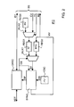
- FIG. 2 is a block diagram that illustrates an interface circuit that forms part of the universal serial bus device.
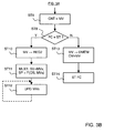
- FIG. 3A and 3B are flowchart diagrams that illustrate operations that the universal serial bus device carries out.
- FIG. 1 illustrates a universal serial bus device USBDV.
- the universal serial bus device USBDV comprises an interface circuit IFC, a central processing unit CPU, a program memory PMEM, a data memory DMEM, and a bus BS.
- the bus BS constitutes a path via which the aforementioned elements may exchange data, including control data.
- the universal serial bus device USBDV carries out various different operations, such as, for example, an authentication on the basis of electronic keys.
- the program memory PMEM comprises a set of instructions, i.e. software, which causes the central processing unit CPU to effect these various different operations.
- the data memory DMEM stores intermediate results of the operations.
- An operation may be defined by a software module, such as, for example, a subroutine.
- the program memory PMEM also comprises software for carrying out internal control functions to ensure a suitable operation of the universal serial bus device USBDV.
- the interface circuit IFC converts external data XDT into internal data IDT, and vice versa.
- the external data XDT and the internal data IDT have substantially different formats.
- the external data XDT has a format that is in accordance with a universal serial bus standard. Accordingly, the external data XDT may be a serial bitstream represented by means of a differential signal having a so-called DM component and a so-called DP component. Alternatively, a single-ended signal may also represent the external data XDT.
- the external data XDT that the interface circuit IFC receives is synchronous with a clock signal, which is generated at a transmission end with relatively great precision. Consequently, each bit in the external data XDT has a precise duration.
- the external data XDT comprises predefined bit patterns for the purpose of synchronization and signaling.
- the interface circuit IFC recognizes those predefined bit patterns and takes appropriate action in response thereto.
- the interface circuit IFC Conversely, in a transmission mode, which corresponds to a so-called upstream traffic, the interface circuit IFC generates the required predefined bit patterns for the purpose of synchronization and signaling.
- the internal data IDT has a format that is commonly used in data transmission via an internal bus BS. Respective bits of binary value are transmitted in parallel rather than in series and at a rate that is generally different.
- FIG. 2 illustrates the interface circuit IFC.
- the interface circuit IFC comprises a data reception-and-transmission circuit DRTC, a synchronization circuit SYNC, an oscillator circuit OSC, two multiplexers MUX1, MUX2, and three registers REG1, REG2, REG3.
- the data reception-and-transmission circuit DRTC detects the aforementioned predefined bit patterns that are comprised in the external data XDT received. In response thereto, the data reception-and-transmission circuit DRTC provides control signals CS for multiplexer MUX1 and the synchronization circuit SYNC.
- the oscillator circuit OSC provides a set of multiphase oscillator signals OS in which each oscillator signal has a different phase.
- the different phases may be, for example, 0°, 45°, 90°, 135°, 180°, 225°, 270° and 315°.
- the oscillator circuit OSC may be, for example, similar to the free-running oscillator circuit described in US patent application published under number 2004/0148539.
- FIG. 10 of that patent publication illustrates the free-running oscillator circuit.
- the oscillator OSC may be implemented in the form of, for example, a CMOS integrated circuit. In that case, the set of multiphase oscillator signals OS will have a precision that is characterized by the following items:
- the synchronization circuit SYNC generates a sampling signal SP on the basis of the set of multiphase oscillator signals OS, the control signals CS, and a synchronization value SV.
- the data reception-and-transmission circuit DRTC samples the external data XDT received on the basis of the sampling signal SP. This sampling constitutes an important step in conversion of external data XDT into internal data IDT.
- the sampling signal SP may comprise, for example, sampling edges. Preferably, each sampling edge substantially occurs at the middle of a bit period. The closer the sampling edge is to the middle of the bit period, the more reliable and robust data reception will be.
- the synchronization value SV determines the position of the sampling edge within a bit period in terms of number of cycles within the set of multiphase oscillator signals OS.
- the synchronization value SV can be a reset value RV, which is stored in register REG3, a calibration value CV, which is stored in a nonvolatile location of the data memory DMEM, or a stored measured value MVs, which is stored in register REG2.
- Multiplexer MUX2 receives the reset value RV, which is stored in register REG3.
- Register REG3 may be a so-called wired register that contains a fixed value, which is functionally equivalent to a read-only memory.
- Multiplexer MUX2 further receives the calibration value CV, which is stored in a nonvolatile location of the data memory DMEM.
- Multiplexer MUX2 either transmits the reset value RV or the calibration value CV depending on a calibration flag FC that is stored in a non-volatile location of the data memory DMEM.
- the transmitted value which is either the reset value RV or the calibration value CV, is stored in register REG1.
- the value that is stored in register REG1 constitutes an initial value IV.
- Multiplexer MUX1 receives the initial value IV and the stored measured value MVs, which is present in register REG2.
- the stored measured value MVs is a measured value MV that the synchronization circuit SYNC has established and that has been stored in register REG2.
- the measured value MV may also be transferred to a nonvolatile memory location of the data memory DMEM via the bus BS.
- Multiplexer MUX1 either applies the initial value IV or the stored measured value MVs to the synchronization circuit SYNC depending on the control signals CS from the data reception-and-transmission circuit DRTC.
- FIGS. 3A and 3B further illustrate the operation of the universal serial bus device USBDV, which is illustrated in FIG. 1, and the interface circuit IFC that forms part thereof and which has been illustrated in FIG. 2.
- FIG. 3A illustrates a first series of steps.
- FIG. 3B illustrates a subsequent series of steps.
- a first step ST1 the universal serial bus device USBDV, which is illustrated in FIG. 1, is coupled to a universal serial bus host. This initiates a so-called power up phase in which mutual recognition takes place (PWUP).
- PWUP power up phase in which mutual recognition takes place
- the universal serial bus device USBDV carries out a second-alternative third step ST3B if the calibration flag FC has not been set.
- a fourth step ST4 the data reception-and-transmission circuit DRTC, which is illustrated in FIG. 2, checks whether a predefined bit pattern has started or not (STRT N bit ?). It is assumed that the predefined bit pattern comprises N bits, N being an integer value, such as, for example, 4 or 8.
- the fourth step ST4 may be implemented in the form of, for example, a detection circuit specifically arranged to detect one or more predefined bit patterns.
- the control signals CS which are illustrated in FIG. 2, signal the start of a predefined bit pattern.
- the predefined bit pattern may be, for example, a Synchronization Packet followed by the Packet Identifier within which there is an even number of bits (4 or 8).
- the predefined bit pattern may comprise two consecutives Start Of Frame (SOF) marks within which there are typically 12,000 bits.
- SOF Start Of Frame
- the universal serial bus device USBDV carries out a fifth step ST5, a sixth step ST6, and a seventh step ST7, if the data reception-and-transmission circuit DRTC has detected the predefined bit pattern.
- the synchronization circuit SYNC counts cycles of an oscillator signal comprised in the set of multiphase oscillator signals OS that the oscillator circuit OSC provides (CNT OS).
- the synchronization circuit SYNC may comprise a dedicated counter.
- the synchronization circuit SYNC generates the sampling signal SP in the following manner.
- the control signals CS signal the start of a bit period.
- the synchronization circuit SYNC counts the number of cycles of an oscillator signal comprised in a set of multiphase oscillator signals OS.
- the synchronization circuit SYNC provides a sampling edge when the number of cycles corresponds to the initial value IV. Accordingly, the position of the sampling edge within the bit period concerned is a function of the frequency of the oscillator signal and the initial value IV.
- the frequency of the oscillator signal may be relatively imprecise.
- the frequency may have any value in a relatively wide frequency range, for example, between 33 and 66 MHz.
- the initial value IV should preferably compensate this imprecision to a certain extent.
- the data reception-and-transmission circuit DRTC checks whether the predefined bit period has ended or not (END N bit ?).
- the seventh step ST7 may be implemented in the form of, for example, the detection circuit mentioned hereinbefore with respect to the fourth step ST4.
- the control signals CS which are illustrated in FIG. 2, signal the end of the predefined bit pattern.
- the fifth step ST5, the sixth step ST6, and the seventh step ST7 constitute a loop.
- the loop has a duration that corresponds to N bits periods.
- the loop is entered into at the fourth step ST4 when the predefined bit pattern starts.
- the loop is left at the seventh step ST7 when the predefined bit pattern ends.
- the synchronization circuit SYNC counts the number of cycles of the oscillator signal during the loop in the fifth step ST5. Accordingly, the number of cycles at the end of the loop corresponds to N bits period.
- the synchronization circuit SYNC determines how many cycles of the oscillator signal are comprised in a one-bit period. It is sufficient to divide the number of cycles counted hereinbefore by N, which is the number of bits comprised in the predefined bit pattern.
- the measured value need not necessarily be an integer value.
- the measured value may have an integer portion and a fractional portion.
- the fractional portion may be expressed in units of 1 ⁇ 8 of the period of the oscillator signal. For example, the measured value may be 335 ⁇ 8, 33 being the integer portion and 5 ⁇ 8 being the fractional portion.
- the universal serial bus device USBDV carries out a tenth step ST10, an eleventh step ST11, and a twelfth step ST12, if the calibration flag FC has been set.
- the measured value MV is stored into register REG2 so as to become the stored measured value MVs (MV ⁇ REG2).
- the sampling signal SP is a periodic signal having a frequency that corresponds to the frequency of the set of multiphase oscillator signals OS divided by the measured value MV.
- the measured value MV may have a fractional portion.
- the universal serial bus device USBDV continues to calculate further measured values on the occurrence of subsequent predefined bit patterns.
- a newly calculated measured value MV will replace the stored measured value MVs in register REG2 (UPD MVs).
- the stored measured value MVs is continuously updated on the basis of the downstream traffic. This allows compensating for thermal drifts and aging, which contributes to a reliable and robust data communication.
- the continuous update of the stored measured value MVS allows a correction of rounding errors.
- the stored measured value MVs should ideally be 33.600 but that the stored measured value MVs can be expressed in 1/8 th units only. In that case, the stored measured value MVs is set to be 335 ⁇ 8 for 4 consecutive time intervals and 331 ⁇ 2 for 1 subsequent time interval.
- the universal serial bus device USBDV carries out a thirteenth step ST13 and a fourteenth step ST14 if the calibration flag FC has not been set.
- the universal serial bus device USBDV sets the calibration flag FC (ST FC) so that the initial value IV will be the calibration value CV hereinafter.
- the universal serial bus device USBDV described hereinbefore is preferably manufactured in the following manner.
- the universal serial bus device USBDV is manufactured in the form of, for example, an integrated circuit.
- the calibration flag FC which is present in the data memory DMEM, is not set.
- external data XDT is applied to the universal serial bus device USBDV.
- the finishing manufacturing step will cause the universal serial bus device USBDV to establish a measured value that will be the calibration value CV in subsequent operations at the customer end. Accordingly, the imprecision of the oscillator circuit OSC is compensated for on shipped products.
- a data communication device comprises an input circuit (data reception-and-transmission circuit DRTC) that converts external data (XDT) into internal data (IDT) on the basis of a sampling signal (SP).
- a synchronization circuit (SYNC) provides the sampling signal (SP) on the basis of an oscillator signal (set of multiphase oscillator signals OS) and a synchronization value (SV).
- the synchronization value is representative of a number of cycles of the oscillator signal contained within a time interval for a unit of external data (a bit constitutes a unit of data, SV represents the number of cycles in a one-bit period).
- the synchronization value (SV) is an initial value (IV) during an initial synchronization phase (steps ST4-ST8) and a measured value (MV) during a measurement-based synchronization phase (ST11-ST13).
- a control circuit central processing unit CPU in combination with the interface circuit IFC carries out a calibration step (calibration flag FC not set: ST1, ST2, ST3B, ST4-ST9, ST14) in which the initial value (IV) is a preprogrammed reset value (RV) and in which the measured value (MV) is stored as a calibration value (CV).
- the control circuit (CPU, IFC) applies the calibration value (CV) as the initial value (IV) in subsequent initial synchronization phases.
- the aforementioned characteristics can be implemented in numerous different manners. In order to illustrate this, some alternatives are briefly indicated.
- the calibration value CV may be stored in a memory other than the data memory DMEM.
- the interface circuit IFC may comprise a further register for internal storage of the calibration value CV.
- the multiplexers MUX1, MUX2, which are illustrated in FIG. 2 may be replaced by other circuits and/or suitable software in, for example, the program memory PMEM.
- Control functions in relation to the operations illustrated in FIG. 3A and 3B, may substantially be carried out by the interface circuit IFC in an autonomous manner. Alternatively, these functions may substantially be carried out under the control of the central processing unit CPU.
- a set of multiphase oscillator signals OS is advantageous as explained hereinbefore, the oscillator circuit OSC may provide a simple oscillator signal if, for example, less precision is required or if higher frequency circuits are available.
Landscapes
- Engineering & Computer Science (AREA)
- Computer Networks & Wireless Communication (AREA)
- Signal Processing (AREA)
- Information Transfer Systems (AREA)
- Communication Control (AREA)
- Synchronisation In Digital Transmission Systems (AREA)
Abstract
Description
- An aspect of the invention relates to a data communication device. The data communication device may be, for example, a device that communicates data in accordance with a universal serial bus (USB) standard. Other aspects of the invention relate to a method of manufacturing such a data communication device, a method of data communication, a computer program product, and a data processing system. The data processing system may comprise, for example, a desktop or laptop computer and a security device that exchange data in accordance with the USB standard. The security device may be in the form of, for example, a smartcard in accordance with the ISO7816-12 standard or a token that can be coupled to a USB port of the computer.
- United States patent application published under number 2004/0148539 describes a device that generates a local clock period from a USB downstream-received bit-serial signal. The device does not require the use of a crystal or resonator. Counters are used to determine a first number of periods of a free-running high-frequency clock signal contained within a known number of bit periods of the downstream-received bit-serial signal. The first number of periods is divided by the known number of bit periods of the received bit-serial signal to determine a second number of periods of the free-running high-frequency clock signal comprised in a single bit period of the received bit-serial signal. The local clock period is generated on the basis of the free-running high-frequency clock signal and the second number of periods. The local clock period may be phase-locked with the received bit serial signal. The local period is updated on an ongoing manner by downstream known received traffic.
- According to an aspect of the invention, a data communication device has the following characteristics. A data communication device comprises an input circuit that converts external data into internal data on the basis of a sampling signal. A synchronization circuit provides the sampling signal on the basis of an oscillator signal and a synchronization value. The synchronization value is representative of a number of cycles of the oscillator signal contained within a time interval for a unit of external data. The synchronization value is an initial value during an initial synchronization phase and a measured value during a measurement-based synchronization phase. A control circuit carries out a calibration step in which the initial value is a preprogrammed reset value and in which the measured value is stored as a calibration value. The control circuit applies the calibration value as the initial value in subsequent initial synchronization phases.
- The invention takes the following aspects into consideration. Reliability and robustness of data communication with a device of the subject type substantially depends on the precision of the sampling signal in terms of time and frequency. In many applications, the external data comprises a sequence of data units, such as, for example, bits, wherein each data unit occurs within a particular time interval. Ideally, the sampling signal should cause the input circuit to decide upon the value of the relevant data unit in the middle of that time interval. In that case, data communication artifacts such as interference or jitter have the least influence.
- In the prior-art device, the sampling signal, which is referred to as local clock period, is generated on the basis of a stable but relatively imprecise free-running oscillator. Nevertheless, the local clock period can be relatively precise by counting the number of free-running oscillator cycles in a predefined pattern of N bits, N being an integer. Accordingly, a one-bit period is defined with relatively great precision in terms of the counted number of free-running oscillator cycles divided by N. The free-running oscillator cycles are first counted during an initial synchronization phase after a power-up sequence. In that phase, an initial value determines the respective instances when the external data is sampled. The initial value is a preprogrammed fixed value, which represents a nominal number of free-running oscillator cycles in a one-bit period. Since the free-running oscillator cycles are relatively imprecise, the sampling during the initial synchronization phase is relatively imprecise too. This may jeopardize a correct count of the number of free-running oscillator cycles, which prevents any further synchronization. In that case, data communication will be unreliable or even impossible.
- In accordance with the aforementioned aspect of the invention, a control circuit carries out a calibration step in which the initial value is a preprogrammed reset value and in which the measured value, which is a clock cycle count, is stored as a calibration value. The control circuit applies the calibration value as the initial value in subsequent initial synchronization phases.
- Accordingly, the preprogrammed reset value needs to be used only during the initial synchronization phase within the calibration step. The calibration step can be carried out under controlled conditions at, for example, a manufacturing site or another site before customer delivery. Once the calibration step has been carried out, subsequent synchronization phases will use the calibration value, which is based on a measured value, a count of oscillator cycles. The calibration value compensates for oscillator-frequency imprecision due to production spread, which may be significant in particular in integrated circuit implementations. Since the calibration value is used as the initial value in subsequent initial synchronization phases, which will occur at a customer end, the sampling signal will be more precise during those phases. Moreover, the synchronization circuit needs to compensate for temperature variations and aging only, because production spread has already been accounted for by the calibration value. Consequently, there is a significant higher probability that successful synchronization will be achieved for a particular data communication session at the customer end. For those reasons, the invention allows a more robust and reliable data communication.
- These and other aspects of the invention will be described in greater detail hereinafter with reference to drawings.
- FIG. 1 is a block diagram that illustrates a universal serial bus device.
- FIG. 2 is a block diagram that illustrates an interface circuit that forms part of the universal serial bus device.
- FIG. 3A and 3B are flowchart diagrams that illustrate operations that the universal serial bus device carries out.
- FIG. 1 illustrates a universal serial bus device USBDV. The universal serial bus device USBDV comprises an interface circuit IFC, a central processing unit CPU, a program memory PMEM, a data memory DMEM, and a bus BS. The bus BS constitutes a path via which the aforementioned elements may exchange data, including control data.
- The universal serial bus device USBDV carries out various different operations, such as, for example, an authentication on the basis of electronic keys. The program memory PMEM comprises a set of instructions, i.e. software, which causes the central processing unit CPU to effect these various different operations. The data memory DMEM stores intermediate results of the operations. An operation may be defined by a software module, such as, for example, a subroutine. The program memory PMEM also comprises software for carrying out internal control functions to ensure a suitable operation of the universal serial bus device USBDV.
- The interface circuit IFC converts external data XDT into internal data IDT, and vice versa. The external data XDT and the internal data IDT have substantially different formats. The external data XDT has a format that is in accordance with a universal serial bus standard. Accordingly, the external data XDT may be a serial bitstream represented by means of a differential signal having a so-called DM component and a so-called DP component. Alternatively, a single-ended signal may also represent the external data XDT. The external data XDT that the interface circuit IFC receives is synchronous with a clock signal, which is generated at a transmission end with relatively great precision. Consequently, each bit in the external data XDT has a precise duration.
- Moreover, the external data XDT comprises predefined bit patterns for the purpose of synchronization and signaling. In a reception mode, which corresponds to a so-called downstream traffic, the interface circuit IFC recognizes those predefined bit patterns and takes appropriate action in response thereto. Conversely, in a transmission mode, which corresponds to a so-called upstream traffic, the interface circuit IFC generates the required predefined bit patterns for the purpose of synchronization and signaling.
- The internal data IDT has a format that is commonly used in data transmission via an internal bus BS. Respective bits of binary value are transmitted in parallel rather than in series and at a rate that is generally different.
- FIG. 2 illustrates the interface circuit IFC. The interface circuit IFC comprises a data reception-and-transmission circuit DRTC, a synchronization circuit SYNC, an oscillator circuit OSC, two multiplexers MUX1, MUX2, and three registers REG1, REG2, REG3. The data reception-and-transmission circuit DRTC detects the aforementioned predefined bit patterns that are comprised in the external data XDT received. In response thereto, the data reception-and-transmission circuit DRTC provides control signals CS for multiplexer MUX1 and the synchronization circuit SYNC.
- The oscillator circuit OSC provides a set of multiphase oscillator signals OS in which each oscillator signal has a different phase. The different phases may be, for example, 0°, 45°, 90°, 135°, 180°, 225°, 270° and 315°. The oscillator circuit OSC may be, for example, similar to the free-running oscillator circuit described in US patent application published under number 2004/0148539. FIG. 10 of that patent publication illustrates the free-running oscillator circuit. The oscillator OSC may be implemented in the form of, for example, a CMOS integrated circuit. In that case, the set of multiphase oscillator signals OS will have a precision that is characterized by the following items:
- Short-term stability of ±0.01%, over a few milliseconds;
- Production spread of ±20%, chip-to-chip, wafer-to-wafer, foundry to foundry;
- Thermal drift of ±3 % over 60°C;
- Packaging influence of ±1%; and
- Aging of ±1%.
- The synchronization circuit SYNC generates a sampling signal SP on the basis of the set of multiphase oscillator signals OS, the control signals CS, and a synchronization value SV. The data reception-and-transmission circuit DRTC samples the external data XDT received on the basis of the sampling signal SP. This sampling constitutes an important step in conversion of external data XDT into internal data IDT. The sampling signal SP may comprise, for example, sampling edges. Preferably, each sampling edge substantially occurs at the middle of a bit period. The closer the sampling edge is to the middle of the bit period, the more reliable and robust data reception will be. The synchronization value SV determines the position of the sampling edge within a bit period in terms of number of cycles within the set of multiphase oscillator signals OS.
- The synchronization value SV can be a reset value RV, which is stored in register REG3, a calibration value CV, which is stored in a nonvolatile location of the data memory DMEM, or a stored measured value MVs, which is stored in register REG2. Multiplexer MUX2 receives the reset value RV, which is stored in register REG3. Register REG3 may be a so-called wired register that contains a fixed value, which is functionally equivalent to a read-only memory. Multiplexer MUX2 further receives the calibration value CV, which is stored in a nonvolatile location of the data memory DMEM. Multiplexer MUX2 either transmits the reset value RV or the calibration value CV depending on a calibration flag FC that is stored in a non-volatile location of the data memory DMEM. The transmitted value, which is either the reset value RV or the calibration value CV, is stored in register REG1.
- The value that is stored in register REG1 constitutes an initial value IV. Multiplexer MUX1 receives the initial value IV and the stored measured value MVs, which is present in register REG2. The stored measured value MVs is a measured value MV that the synchronization circuit SYNC has established and that has been stored in register REG2. The measured value MV may also be transferred to a nonvolatile memory location of the data memory DMEM via the bus BS. Multiplexer MUX1 either applies the initial value IV or the stored measured value MVs to the synchronization circuit SYNC depending on the control signals CS from the data reception-and-transmission circuit DRTC.
- FIGS. 3A and 3B further illustrate the operation of the universal serial bus device USBDV, which is illustrated in FIG. 1, and the interface circuit IFC that forms part thereof and which has been illustrated in FIG. 2. FIG. 3A illustrates a first series of steps. FIG. 3B illustrates a subsequent series of steps.
- In a first step ST1, the universal serial bus device USBDV, which is illustrated in FIG. 1, is coupled to a universal serial bus host. This initiates a so-called power up phase in which mutual recognition takes place (PWUP). In a second step ST2, it is checked whether a calibration flag FC has been set or not (FC=ST?). The universal serial bus device USBDV carries out a first-alternative third step ST3A if the calibration flag FC has been set. In this step, the calibration value CV is read from the data memory DMEM, which is illustrated in FIG. 1, and stored in register REG1 as the initial value IV via multiplexer MUX2, which is illustrated in FIG. 2 (MUX2 : IV=CV). The universal serial bus device USBDV carries out a second-alternative third step ST3B if the calibration flag FC has not been set. In this step, the reset value RV is read from register REG3 and stored in register REG2 as the initial value IV via multiplexer MUX2 (MUX2 : IV=RV).
- In a fourth step ST4, the data reception-and-transmission circuit DRTC, which is illustrated in FIG. 2, checks whether a predefined bit pattern has started or not (STRT N bit ?). It is assumed that the predefined bit pattern comprises N bits, N being an integer value, such as, for example, 4 or 8. The fourth step ST4 may be implemented in the form of, for example, a detection circuit specifically arranged to detect one or more predefined bit patterns. The control signals CS, which are illustrated in FIG. 2, signal the start of a predefined bit pattern. In a Low Speed, the predefined bit pattern may be, for example, a Synchronization Packet followed by the Packet Identifier within which there is an even number of bits (4 or 8). In a Full Speed, the predefined bit pattern may comprise two consecutives Start Of Frame (SOF) marks within which there are typically 12,000 bits.
- The universal serial bus device USBDV carries out a fifth step ST5, a sixth step ST6, and a seventh step ST7, if the data reception-and-transmission circuit DRTC has detected the predefined bit pattern. In the fifth step ST5, the synchronization circuit SYNC counts cycles of an oscillator signal comprised in the set of multiphase oscillator signals OS that the oscillator circuit OSC provides (CNT OS). To that end, the synchronization circuit SYNC may comprise a dedicated counter. In the sixth step ST6, the synchronization circuit SYNC generates the sampling signal SP on the basis of the control signals CS, the set of multiphase oscillator signals OS, and the initial value IV, which constitutes the synchronization value SV (MLTX1: SV=IV; SP = F(CS, OS, IV)).
- The synchronization circuit SYNC generates the sampling signal SP in the following manner. The control signals CS signal the start of a bit period. The synchronization circuit SYNC counts the number of cycles of an oscillator signal comprised in a set of multiphase oscillator signals OS. The synchronization circuit SYNC provides a sampling edge when the number of cycles corresponds to the initial value IV. Accordingly, the position of the sampling edge within the bit period concerned is a function of the frequency of the oscillator signal and the initial value IV. The frequency of the oscillator signal may be relatively imprecise. The frequency may have any value in a relatively wide frequency range, for example, between 33 and 66 MHz. The initial value IV should preferably compensate this imprecision to a certain extent.
- In the seventh step ST7, the data reception-and-transmission circuit DRTC checks whether the predefined bit period has ended or not (END N bit ?). The seventh step ST7 may be implemented in the form of, for example, the detection circuit mentioned hereinbefore with respect to the fourth step ST4. The control signals CS, which are illustrated in FIG. 2, signal the end of the predefined bit pattern.
- Accordingly, the fifth step ST5, the sixth step ST6, and the seventh step ST7 constitute a loop. The loop has a duration that corresponds to N bits periods. The loop is entered into at the fourth step ST4 when the predefined bit pattern starts. The loop is left at the seventh step ST7 when the predefined bit pattern ends. The synchronization circuit SYNC counts the number of cycles of the oscillator signal during the loop in the fifth step ST5. Accordingly, the number of cycles at the end of the loop corresponds to N bits period.
- In an eighth step ST8, which is illustrated in FIG. 3B, the synchronization circuit SYNC determines how many cycles of the oscillator signal are comprised in a one-bit period. It is sufficient to divide the number of cycles counted hereinbefore by N, which is the number of bits comprised in the predefined bit pattern. The number of cycles comprised in a one-bit period constitutes the measured value (CNT = MV). The measured value need not necessarily be an integer value. The measured value may have an integer portion and a fractional portion. The fractional portion may be expressed in units of ⅛ of the period of the oscillator signal. For example, the measured value may be 33⅝, 33 being the integer portion and ⅝ being the fractional portion.
- In a ninth step ST9, the universal serial bus device USBDV checks anew whether the calibration flag FC has been set or not, similar to the second step ST2 (FC = ST ?). The universal serial bus device USBDV carries out a tenth step ST10, an eleventh step ST11, and a twelfth step ST12, if the calibration flag FC has been set. In the tenth step ST10, the measured value MV is stored into register REG2 so as to become the stored measured value MVs (MV → REG2). In the eleventh step ST11, the synchronization circuit SYNC generates the sampling signal SP on the basis of the set of multiphase oscillator signals OS and the stored measured value MVs (MUX1: SV=MVs; SP = F(OS, MVs). The sampling signal SP is a periodic signal having a frequency that corresponds to the frequency of the set of multiphase oscillator signals OS divided by the measured value MV.
- It is recalled that the measured value MV may have a fractional portion. The synchronization circuit SYNC takes into account the fractional portion by selecting an oscillator signal that has an appropriate phase among the set of multiphase oscillator signals OS. It is thus possible to simulate a higher oscillator frequency, which allows greater precision. For example, let it be assumed that the set of multiphase oscillator signals OS have a frequency of 50 MHz and that the measured value MV is 33⅝. In that case, the sampling signal SP that the synchronization circuit SYNC generates will have a period that is equal to 20 nanoseconds (ns) multiplied with 33⅝, which corresponds to 672.5 ns. The period of the sampling signal SP can thus be adjusted with a granularity of 20/8 = 0.25 ns, which corresponds to a cycle of a 400 MHz clock signal.
- In the twelfth step ST12, the universal serial bus device USBDV continues to calculate further measured values on the occurrence of subsequent predefined bit patterns. A newly calculated measured value MV will replace the stored measured value MVs in register REG2 (UPD MVs). Accordingly, the stored measured value MVs is continuously updated on the basis of the downstream traffic. This allows compensating for thermal drifts and aging, which contributes to a reliable and robust data communication. In that respect, it should be noted that the continuous update of the stored measured value MVS allows a correction of rounding errors. For example, let it be assumed that the stored measured value MVs should ideally be 33.600 but that the stored measured value MVs can be expressed in 1/8th units only. In that case, the stored measured value MVs is set to be 33⅝ for 4 consecutive time intervals and 33½ for 1 subsequent time interval.
- Returning to the ninth step ST9, the universal serial bus device USBDV carries out a thirteenth step ST13 and a fourteenth step ST14 if the calibration flag FC has not been set. In the thirteenth step ST13, the universal serial bus device USBDV stores the measured value MV, which has been calculated in the preceding steps, in a nonvolatile location of the data memory DMEM, which is illustrated in FIG. 1 (MV → DMEM). This storage causes the measured value to be the calibration value CV (CM=MV), which will be available as such at the occurrence of a subsequent power up phase. In the fourteenth step ST14, the universal serial bus device USBDV sets the calibration flag FC (ST FC) so that the initial value IV will be the calibration value CV hereinafter.
- The universal serial bus device USBDV described hereinbefore is preferably manufactured in the following manner. In a device manufacturing step, the universal serial bus device USBDV is manufactured in the form of, for example, an integrated circuit. The calibration flag FC, which is present in the data memory DMEM, is not set. In a finishing manufacturing step, external data XDT is applied to the universal serial bus device USBDV. The finishing manufacturing step will cause the universal serial bus device USBDV to establish a measured value that will be the calibration value CV in subsequent operations at the customer end. Accordingly, the imprecision of the oscillator circuit OSC is compensated for on shipped products.
- The detailed description hereinbefore with reference to the drawings illustrates the following characteristics. A data communication device (USBDV) comprises an input circuit (data reception-and-transmission circuit DRTC) that converts external data (XDT) into internal data (IDT) on the basis of a sampling signal (SP). A synchronization circuit (SYNC) provides the sampling signal (SP) on the basis of an oscillator signal (set of multiphase oscillator signals OS) and a synchronization value (SV). The synchronization value (SV) is representative of a number of cycles of the oscillator signal contained within a time interval for a unit of external data (a bit constitutes a unit of data, SV represents the number of cycles in a one-bit period). The synchronization value (SV) is an initial value (IV) during an initial synchronization phase (steps ST4-ST8) and a measured value (MV) during a measurement-based synchronization phase (ST11-ST13). A control circuit (central processing unit CPU in combination with the interface circuit IFC) carries out a calibration step (calibration flag FC not set: ST1, ST2, ST3B, ST4-ST9, ST14) in which the initial value (IV) is a preprogrammed reset value (RV) and in which the measured value (MV) is stored as a calibration value (CV). The control circuit (CPU, IFC) applies the calibration value (CV) as the initial value (IV) in subsequent initial synchronization phases.
- The aforementioned characteristics can be implemented in numerous different manners. In order to illustrate this, some alternatives are briefly indicated. The calibration value CV may be stored in a memory other than the data memory DMEM. For example, the interface circuit IFC may comprise a further register for internal storage of the calibration value CV. The multiplexers MUX1, MUX2, which are illustrated in FIG. 2, may be replaced by other circuits and/or suitable software in, for example, the program memory PMEM. Control functions in relation to the operations illustrated in FIG. 3A and 3B, may substantially be carried out by the interface circuit IFC in an autonomous manner. Alternatively, these functions may substantially be carried out under the control of the central processing unit CPU. Although a set of multiphase oscillator signals OS is advantageous as explained hereinbefore, the oscillator circuit OSC may provide a simple oscillator signal if, for example, less precision is required or if higher frequency circuits are available.
- There are numerous ways of implementing functions by means of items of hardware or software, or both. In this respect, the drawings are very diagrammatic, each representing only one possible embodiment of the invention. Thus, although a drawing shows different functions as different blocks, this by no means excludes that a single item of hardware or software carries out several functions. Nor does it exclude that an assembly of items of hardware or software or both carry out a function.
- The remarks made herein before demonstrate that the detailed description with reference to the drawings, illustrate rather than limit the invention. There are numerous alternatives, which fall within the scope of the appended claims. Any reference sign in a claim should not be construed as limiting the claim. The word "comprising" does not exclude the presence of other elements or steps than those listed in a claim. The word "a" or "an" preceding an element or step does not exclude the presence of a plurality of such elements or steps.
Claims (8)
- A data communication device comprising:- an input circuit arranged to convert external data into internal data on the basis of a sampling signal;- a synchronization circuit arranged to provide the sampling signal on the basis of an oscillator signal and a synchronization value that is representative of a number of cycles of the oscillator signal contained within a time interval for a unit of external data, the synchronization value being an initial value during an initial synchronization phase and a measured value during a measurement-based synchronization phase; and- a control circuit arranged to carry out a calibration step in which the initial value is a preprogrammed reset value and in which the measured value is stored as a calibration value, the control circuit being arranged to apply the calibration value as the initial value for subsequent initial synchronization phases.
- A data communication device as claimed in claim 1, wherein the input circuit is arranged to receive and transmit a bit-serial stream in accordance with a universal serial bus standard.
- A data communication device as claimed in claim 1, wherein the oscillator circuit is arranged to provide a set of multiphase oscillator signals and wherein the synchronization circuit is arranged to select an oscillator signal therefrom on the basis of a fractional part in the measured value.
- A method of manufacturing a data communication device as claimed in claim 1, the method comprising a finishing step in which the data communication device is caused to carry out the calibration step while applying external data to the data communication device.
- A method of data communication that employs a data communication device comprising:- an input circuit arranged to convert external data into internal data on the basis of a sampling signal; and- a synchronization circuit arranged to provide the sampling signal on the basis of an oscillator signal and a synchronization value that is representative of a number of cycles of the oscillator signal contained within a time interval for a unit of data in the received external signal;the method comprising;- an initial synchronization step during which an initial value constitutes the synchronization value and during which a measured value is established on the basis of a count of cycles of the oscillator signal within a time interval for N units of data, N being an integer;- a measurement-based synchronization step during which the measured value constitutes the synchronization value; and- a calibration step in which the initial value is a preprogrammed reset value and in which the measured value is stored as a calibration value, the calibration value being applied as the initial value for subsequent initial synchronization steps.
- A computer program product for a data communication device comprising:- an input circuit arranged to convert received external data into internal data on the basis of a sampling signal; and- a synchronization circuit arranged to provide the sampling signal on the basis of an oscillator signal and a synchronization value that is representative of a number of cycles of the oscillator signal contained within a time interval for a unit of data in the received external signal;the computer program product comprising a set of instructions that, when loaded into a program memory of the data communication device, causes the data communication device to carry out:- an initial synchronization step during which an initial value constitutes the synchronization value and during which a measured value is established on the basis of a count of cycles of the oscillator signal within a time interval for N units of data, N being an integer;- a measured synchronization step during which the measured value constitutes the synchronization value; and- a calibration step in which the initial value is a preprogrammed reset value and in which the measured value is stored as a calibration value, the calibration value being applied as the initial value for subsequent initial synchronization steps.
- A data processing system comprising a computer and a data communication device as claimed in claim 1, which is connectable to the computer.
- A data processing system comprising a computer and a data communication device as claimed in claim 2, which is connectable to the computer, the computer being arranged to receive data from the data communication device and to transmit data to the communication device in accordance with the universal serial bus standard.
Priority Applications (4)
| Application Number | Priority Date | Filing Date | Title |
|---|---|---|---|
| DE602005005002T DE602005005002T2 (en) | 2005-01-05 | 2005-01-05 | Device for data communication |
| EP05290013A EP1679819B1 (en) | 2005-01-05 | 2005-01-05 | Data communication device |
| AT05290013T ATE387771T1 (en) | 2005-01-05 | 2005-01-05 | DATA COMMUNICATION DEVICE |
| US11/325,233 US7656979B2 (en) | 2005-01-05 | 2006-01-04 | Data communication device |
Applications Claiming Priority (1)
| Application Number | Priority Date | Filing Date | Title |
|---|---|---|---|
| EP05290013A EP1679819B1 (en) | 2005-01-05 | 2005-01-05 | Data communication device |
Publications (2)
| Publication Number | Publication Date |
|---|---|
| EP1679819A1 true EP1679819A1 (en) | 2006-07-12 |
| EP1679819B1 EP1679819B1 (en) | 2008-02-27 |
Family
ID=34941867
Family Applications (1)
| Application Number | Title | Priority Date | Filing Date |
|---|---|---|---|
| EP05290013A Expired - Lifetime EP1679819B1 (en) | 2005-01-05 | 2005-01-05 | Data communication device |
Country Status (4)
| Country | Link |
|---|---|
| US (1) | US7656979B2 (en) |
| EP (1) | EP1679819B1 (en) |
| AT (1) | ATE387771T1 (en) |
| DE (1) | DE602005005002T2 (en) |
Families Citing this family (14)
| Publication number | Priority date | Publication date | Assignee | Title |
|---|---|---|---|---|
| US7764130B2 (en) | 1999-01-22 | 2010-07-27 | Multigig Inc. | Electronic circuitry |
| GB2377836B (en) | 2000-05-11 | 2004-10-27 | Multigig Ltd | Electronic pulse generator and oscillator |
| WO2004008330A1 (en) * | 2002-07-17 | 2004-01-22 | Fiberbyte Pty Ltd | Synchronized multichannel universal serial bus |
| US8169267B2 (en) | 2007-03-29 | 2012-05-01 | Multigig, Inc. | Wave reversing system and method for a rotary traveling wave oscillator |
| US8913978B2 (en) * | 2007-04-09 | 2014-12-16 | Analog Devices, Inc. | RTWO-based down converter |
| US8742857B2 (en) | 2008-05-15 | 2014-06-03 | Analog Devices, Inc. | Inductance enhanced rotary traveling wave oscillator circuit and method |
| WO2010020015A1 (en) * | 2008-08-21 | 2010-02-25 | Chronologic Pty Ltd | Synchronisation and timing method and apparatus |
| US8487710B2 (en) | 2011-12-12 | 2013-07-16 | Analog Devices, Inc. | RTWO-based pulse width modulator |
| US8581668B2 (en) | 2011-12-20 | 2013-11-12 | Analog Devices, Inc. | Oscillator regeneration device |
| US10277233B2 (en) | 2016-10-07 | 2019-04-30 | Analog Devices, Inc. | Apparatus and methods for frequency tuning of rotary traveling wave oscillators |
| US10312922B2 (en) | 2016-10-07 | 2019-06-04 | Analog Devices, Inc. | Apparatus and methods for rotary traveling wave oscillators |
| US11527992B2 (en) | 2019-09-19 | 2022-12-13 | Analog Devices International Unlimited Company | Rotary traveling wave oscillators with distributed stubs |
| US11264949B2 (en) | 2020-06-10 | 2022-03-01 | Analog Devices International Unlimited Company | Apparatus and methods for rotary traveling wave oscillators |
| US11539353B2 (en) | 2021-02-02 | 2022-12-27 | Analog Devices International Unlimited Company | RTWO-based frequency multiplier |
Citations (3)
| Publication number | Priority date | Publication date | Assignee | Title |
|---|---|---|---|---|
| US5815017A (en) * | 1997-03-03 | 1998-09-29 | Motorola, Inc. | Forced oscillator circuit and method |
| US6064707A (en) * | 1995-12-22 | 2000-05-16 | Zilog, Inc. | Apparatus and method for data synchronizing and tracking |
| US20040148539A1 (en) * | 2003-01-28 | 2004-07-29 | Leydier Robert Antoine | Method and apparatus for clock synthesis using universal serial bus downstream received signals |
Family Cites Families (4)
| Publication number | Priority date | Publication date | Assignee | Title |
|---|---|---|---|---|
| US5588025A (en) * | 1995-03-15 | 1996-12-24 | David Sarnoff Research Center, Inc. | Single oscillator compressed digital information receiver |
| US7003043B2 (en) * | 2002-01-09 | 2006-02-21 | Intel Corporation | Replica driver mismatch correction using a variable offset comparator |
| JP4159338B2 (en) * | 2002-10-18 | 2008-10-01 | 日本テキサス・インスツルメンツ株式会社 | Write pulse generation circuit |
| US20060045215A1 (en) * | 2004-08-31 | 2006-03-02 | Motorola, Inc. | Method and apparatus for frequency correcting a periodic signal |
-
2005
- 2005-01-05 DE DE602005005002T patent/DE602005005002T2/en not_active Expired - Lifetime
- 2005-01-05 AT AT05290013T patent/ATE387771T1/en not_active IP Right Cessation
- 2005-01-05 EP EP05290013A patent/EP1679819B1/en not_active Expired - Lifetime
-
2006
- 2006-01-04 US US11/325,233 patent/US7656979B2/en active Active
Patent Citations (3)
| Publication number | Priority date | Publication date | Assignee | Title |
|---|---|---|---|---|
| US6064707A (en) * | 1995-12-22 | 2000-05-16 | Zilog, Inc. | Apparatus and method for data synchronizing and tracking |
| US5815017A (en) * | 1997-03-03 | 1998-09-29 | Motorola, Inc. | Forced oscillator circuit and method |
| US20040148539A1 (en) * | 2003-01-28 | 2004-07-29 | Leydier Robert Antoine | Method and apparatus for clock synthesis using universal serial bus downstream received signals |
Also Published As
| Publication number | Publication date |
|---|---|
| ATE387771T1 (en) | 2008-03-15 |
| EP1679819B1 (en) | 2008-02-27 |
| DE602005005002T2 (en) | 2008-08-28 |
| US7656979B2 (en) | 2010-02-02 |
| DE602005005002D1 (en) | 2008-04-10 |
| US20060146968A1 (en) | 2006-07-06 |
Similar Documents
| Publication | Publication Date | Title |
|---|---|---|
| EP1679819B1 (en) | Data communication device | |
| CN110520815B (en) | Method and system for adding precise timestamps | |
| CN101401055B (en) | Distributed synchronization and timing system | |
| CN101960771B (en) | Communication system comprising a data bus and several subscriber nodes connected thereto and method for operating such a communication system | |
| US7120813B2 (en) | Method and apparatus for clock synthesis using universal serial bus downstream received signals | |
| EP1311936B1 (en) | Method and device for local clock generation using universal serial bus downstream received signals dp and dm | |
| US8566632B2 (en) | Multi-rate sampling for network receiving nodes using distributed clock synchronization | |
| TWI405118B (en) | A removable memory device, a phase synchronization method, a phase synchronization program, a recording medium thereof, and a host terminal | |
| JP2012500430A (en) | Synchronization and timing method and apparatus | |
| TWI646817B (en) | Method and apparatus for clock recovery | |
| CN109254941B (en) | FPGA-based serial signal clock synchronization method, serial-to-parallel conversion method and device | |
| US11303376B2 (en) | Information processing apparatus and time synchronization method | |
| JP5783017B2 (en) | Oscillator frequency error correction apparatus, frequency error correction method, frequency error correction program, and frequency error correction system | |
| US7864906B2 (en) | System and method for clock signal synchronization | |
| JP2009512050A (en) | Method and circuit for local clock generation, and smart card including the clock above | |
| US8907730B2 (en) | Frequency calibration device and method for programmable oscillator | |
| US8283983B2 (en) | Frequency calibration device and method for programmable oscillator | |
| US10116435B2 (en) | Control circuit and control method of communication device | |
| US9319216B2 (en) | Operating method of human interface device | |
| CN102981995B (en) | The built-in crystal oscillator realizing circuit of USB device interface and method | |
| CN114826465A (en) | System for monitoring execution of clock synchronization function | |
| HK1128098B (en) | Distributed synchronization and timing system | |
| HK1149097B (en) | Distributed synchronization and timing system | |
| JP2003099151A (en) | Clock phase adjustment system and method |
Legal Events
| Date | Code | Title | Description |
|---|---|---|---|
| PUAI | Public reference made under article 153(3) epc to a published international application that has entered the european phase |
Free format text: ORIGINAL CODE: 0009012 |
|
| AK | Designated contracting states |
Kind code of ref document: A1 Designated state(s): AT BE BG CH CY CZ DE DK EE ES FI FR GB GR HU IE IS IT LI LT LU MC NL PL PT RO SE SI SK TR |
|
| AX | Request for extension of the european patent |
Extension state: AL BA HR LV MK YU |
|
| 17P | Request for examination filed |
Effective date: 20061229 |
|
| 17Q | First examination report despatched |
Effective date: 20070131 |
|
| AKX | Designation fees paid |
Designated state(s): AT BE BG CH CY CZ DE DK EE ES FI FR GB GR HU IE IS IT LI LT LU MC NL PL PT RO SE SI SK TR |
|
| GRAP | Despatch of communication of intention to grant a patent |
Free format text: ORIGINAL CODE: EPIDOSNIGR1 |
|
| GRAS | Grant fee paid |
Free format text: ORIGINAL CODE: EPIDOSNIGR3 |
|
| GRAA | (expected) grant |
Free format text: ORIGINAL CODE: 0009210 |
|
| AK | Designated contracting states |
Kind code of ref document: B1 Designated state(s): AT BE BG CH CY CZ DE DK EE ES FI FR GB GR HU IE IS IT LI LT LU MC NL PL PT RO SE SI SK TR |
|
| REG | Reference to a national code |
Ref country code: GB Ref legal event code: FG4D |
|
| RIN1 | Information on inventor provided before grant (corrected) |
Inventor name: POMET, ALAIN,C/O ST MICROELECTRONICS SA Inventor name: LEYDIER, ROBERT,C/O AXALTO S.A. |
|
| REG | Reference to a national code |
Ref country code: CH Ref legal event code: EP |
|
| REG | Reference to a national code |
Ref country code: IE Ref legal event code: FG4D |
|
| REF | Corresponds to: |
Ref document number: 602005005002 Country of ref document: DE Date of ref document: 20080410 Kind code of ref document: P |
|
| PG25 | Lapsed in a contracting state [announced via postgrant information from national office to epo] |
Ref country code: FI Free format text: LAPSE BECAUSE OF FAILURE TO SUBMIT A TRANSLATION OF THE DESCRIPTION OR TO PAY THE FEE WITHIN THE PRESCRIBED TIME-LIMIT Effective date: 20080227 Ref country code: IS Free format text: LAPSE BECAUSE OF FAILURE TO SUBMIT A TRANSLATION OF THE DESCRIPTION OR TO PAY THE FEE WITHIN THE PRESCRIBED TIME-LIMIT Effective date: 20080627 Ref country code: ES Free format text: LAPSE BECAUSE OF FAILURE TO SUBMIT A TRANSLATION OF THE DESCRIPTION OR TO PAY THE FEE WITHIN THE PRESCRIBED TIME-LIMIT Effective date: 20080607 |
|
| ET | Fr: translation filed | ||
| NLV1 | Nl: lapsed or annulled due to failure to fulfill the requirements of art. 29p and 29m of the patents act | ||
| PG25 | Lapsed in a contracting state [announced via postgrant information from national office to epo] |
Ref country code: AT Free format text: LAPSE BECAUSE OF FAILURE TO SUBMIT A TRANSLATION OF THE DESCRIPTION OR TO PAY THE FEE WITHIN THE PRESCRIBED TIME-LIMIT Effective date: 20080227 |
|
| PG25 | Lapsed in a contracting state [announced via postgrant information from national office to epo] |
Ref country code: PL Free format text: LAPSE BECAUSE OF FAILURE TO SUBMIT A TRANSLATION OF THE DESCRIPTION OR TO PAY THE FEE WITHIN THE PRESCRIBED TIME-LIMIT Effective date: 20080227 Ref country code: SI Free format text: LAPSE BECAUSE OF FAILURE TO SUBMIT A TRANSLATION OF THE DESCRIPTION OR TO PAY THE FEE WITHIN THE PRESCRIBED TIME-LIMIT Effective date: 20080227 Ref country code: BE Free format text: LAPSE BECAUSE OF FAILURE TO SUBMIT A TRANSLATION OF THE DESCRIPTION OR TO PAY THE FEE WITHIN THE PRESCRIBED TIME-LIMIT Effective date: 20080227 |
|
| PG25 | Lapsed in a contracting state [announced via postgrant information from national office to epo] |
Ref country code: SK Free format text: LAPSE BECAUSE OF FAILURE TO SUBMIT A TRANSLATION OF THE DESCRIPTION OR TO PAY THE FEE WITHIN THE PRESCRIBED TIME-LIMIT Effective date: 20080227 Ref country code: SE Free format text: LAPSE BECAUSE OF FAILURE TO SUBMIT A TRANSLATION OF THE DESCRIPTION OR TO PAY THE FEE WITHIN THE PRESCRIBED TIME-LIMIT Effective date: 20080527 Ref country code: PT Free format text: LAPSE BECAUSE OF FAILURE TO SUBMIT A TRANSLATION OF THE DESCRIPTION OR TO PAY THE FEE WITHIN THE PRESCRIBED TIME-LIMIT Effective date: 20080721 Ref country code: DK Free format text: LAPSE BECAUSE OF FAILURE TO SUBMIT A TRANSLATION OF THE DESCRIPTION OR TO PAY THE FEE WITHIN THE PRESCRIBED TIME-LIMIT Effective date: 20080227 Ref country code: CZ Free format text: LAPSE BECAUSE OF FAILURE TO SUBMIT A TRANSLATION OF THE DESCRIPTION OR TO PAY THE FEE WITHIN THE PRESCRIBED TIME-LIMIT Effective date: 20080227 Ref country code: NL Free format text: LAPSE BECAUSE OF FAILURE TO SUBMIT A TRANSLATION OF THE DESCRIPTION OR TO PAY THE FEE WITHIN THE PRESCRIBED TIME-LIMIT Effective date: 20080227 |
|
| PG25 | Lapsed in a contracting state [announced via postgrant information from national office to epo] |
Ref country code: RO Free format text: LAPSE BECAUSE OF FAILURE TO SUBMIT A TRANSLATION OF THE DESCRIPTION OR TO PAY THE FEE WITHIN THE PRESCRIBED TIME-LIMIT Effective date: 20080227 |
|
| RAP2 | Party data changed (patent owner data changed or rights of a patent transferred) |
Owner name: STMICROELECTRONICS SA Owner name: GEMALTO SA |
|
| PLBE | No opposition filed within time limit |
Free format text: ORIGINAL CODE: 0009261 |
|
| STAA | Information on the status of an ep patent application or granted ep patent |
Free format text: STATUS: NO OPPOSITION FILED WITHIN TIME LIMIT |
|
| PG25 | Lapsed in a contracting state [announced via postgrant information from national office to epo] |
Ref country code: LT Free format text: LAPSE BECAUSE OF FAILURE TO SUBMIT A TRANSLATION OF THE DESCRIPTION OR TO PAY THE FEE WITHIN THE PRESCRIBED TIME-LIMIT Effective date: 20080227 |
|
| 26N | No opposition filed |
Effective date: 20081128 |
|
| PG25 | Lapsed in a contracting state [announced via postgrant information from national office to epo] |
Ref country code: EE Free format text: LAPSE BECAUSE OF FAILURE TO SUBMIT A TRANSLATION OF THE DESCRIPTION OR TO PAY THE FEE WITHIN THE PRESCRIBED TIME-LIMIT Effective date: 20080227 Ref country code: BG Free format text: LAPSE BECAUSE OF FAILURE TO SUBMIT A TRANSLATION OF THE DESCRIPTION OR TO PAY THE FEE WITHIN THE PRESCRIBED TIME-LIMIT Effective date: 20080527 |
|
| PG25 | Lapsed in a contracting state [announced via postgrant information from national office to epo] |
Ref country code: CY Free format text: LAPSE BECAUSE OF FAILURE TO SUBMIT A TRANSLATION OF THE DESCRIPTION OR TO PAY THE FEE WITHIN THE PRESCRIBED TIME-LIMIT Effective date: 20080227 |
|
| PG25 | Lapsed in a contracting state [announced via postgrant information from national office to epo] |
Ref country code: IT Free format text: LAPSE BECAUSE OF FAILURE TO SUBMIT A TRANSLATION OF THE DESCRIPTION OR TO PAY THE FEE WITHIN THE PRESCRIBED TIME-LIMIT Effective date: 20080227 Ref country code: MC Free format text: LAPSE BECAUSE OF NON-PAYMENT OF DUE FEES Effective date: 20090131 |
|
| REG | Reference to a national code |
Ref country code: CH Ref legal event code: PL |
|
| PG25 | Lapsed in a contracting state [announced via postgrant information from national office to epo] |
Ref country code: CH Free format text: LAPSE BECAUSE OF NON-PAYMENT OF DUE FEES Effective date: 20090131 Ref country code: LI Free format text: LAPSE BECAUSE OF NON-PAYMENT OF DUE FEES Effective date: 20090131 |
|
| PG25 | Lapsed in a contracting state [announced via postgrant information from national office to epo] |
Ref country code: IE Free format text: LAPSE BECAUSE OF NON-PAYMENT OF DUE FEES Effective date: 20090105 |
|
| PG25 | Lapsed in a contracting state [announced via postgrant information from national office to epo] |
Ref country code: GR Free format text: LAPSE BECAUSE OF FAILURE TO SUBMIT A TRANSLATION OF THE DESCRIPTION OR TO PAY THE FEE WITHIN THE PRESCRIBED TIME-LIMIT Effective date: 20080528 |
|
| PG25 | Lapsed in a contracting state [announced via postgrant information from national office to epo] |
Ref country code: LU Free format text: LAPSE BECAUSE OF NON-PAYMENT OF DUE FEES Effective date: 20090105 |
|
| PG25 | Lapsed in a contracting state [announced via postgrant information from national office to epo] |
Ref country code: HU Free format text: LAPSE BECAUSE OF FAILURE TO SUBMIT A TRANSLATION OF THE DESCRIPTION OR TO PAY THE FEE WITHIN THE PRESCRIBED TIME-LIMIT Effective date: 20080828 |
|
| PG25 | Lapsed in a contracting state [announced via postgrant information from national office to epo] |
Ref country code: TR Free format text: LAPSE BECAUSE OF FAILURE TO SUBMIT A TRANSLATION OF THE DESCRIPTION OR TO PAY THE FEE WITHIN THE PRESCRIBED TIME-LIMIT Effective date: 20080227 |
|
| REG | Reference to a national code |
Ref country code: FR Ref legal event code: PLFP Year of fee payment: 12 |
|
| REG | Reference to a national code |
Ref country code: FR Ref legal event code: PLFP Year of fee payment: 13 |
|
| REG | Reference to a national code |
Ref country code: FR Ref legal event code: PLFP Year of fee payment: 14 |
|
| PGFP | Annual fee paid to national office [announced via postgrant information from national office to epo] |
Ref country code: GB Payment date: 20231219 Year of fee payment: 20 |
|
| PGFP | Annual fee paid to national office [announced via postgrant information from national office to epo] |
Ref country code: FR Payment date: 20231219 Year of fee payment: 20 |
|
| PGFP | Annual fee paid to national office [announced via postgrant information from national office to epo] |
Ref country code: DE Payment date: 20231219 Year of fee payment: 20 |
|
| P01 | Opt-out of the competence of the unified patent court (upc) registered |
Effective date: 20240322 |
|
| REG | Reference to a national code |
Ref country code: DE Ref legal event code: R071 Ref document number: 602005005002 Country of ref document: DE |
|
| REG | Reference to a national code |
Ref country code: GB Ref legal event code: PE20 Expiry date: 20250104 |
|
| PG25 | Lapsed in a contracting state [announced via postgrant information from national office to epo] |
Ref country code: GB Free format text: LAPSE BECAUSE OF EXPIRATION OF PROTECTION Effective date: 20250104 |