EP1677366A2 - High output light emitting diode and method for fabricating the same - Google Patents
High output light emitting diode and method for fabricating the same Download PDFInfo
- Publication number
- EP1677366A2 EP1677366A2 EP05292775A EP05292775A EP1677366A2 EP 1677366 A2 EP1677366 A2 EP 1677366A2 EP 05292775 A EP05292775 A EP 05292775A EP 05292775 A EP05292775 A EP 05292775A EP 1677366 A2 EP1677366 A2 EP 1677366A2
- Authority
- EP
- European Patent Office
- Prior art keywords
- type semiconductor
- semiconductor layer
- layer
- led
- sidewalls
- Prior art date
- Legal status (The legal status is an assumption and is not a legal conclusion. Google has not performed a legal analysis and makes no representation as to the accuracy of the status listed.)
- Granted
Links
- 238000000034 method Methods 0.000 title claims abstract description 39
- 239000004065 semiconductor Substances 0.000 claims description 174
- 239000000758 substrate Substances 0.000 claims description 31
- 238000005530 etching Methods 0.000 claims description 16
- 230000000873 masking effect Effects 0.000 claims description 5
- 238000001704 evaporation Methods 0.000 claims description 3
- 230000008569 process Effects 0.000 abstract description 21
- 238000002161 passivation Methods 0.000 abstract description 4
- 230000002349 favourable effect Effects 0.000 abstract 1
- 230000008901 benefit Effects 0.000 description 5
- 239000000463 material Substances 0.000 description 3
- 230000005540 biological transmission Effects 0.000 description 2
- 238000003776 cleavage reaction Methods 0.000 description 2
- 230000000052 comparative effect Effects 0.000 description 2
- 238000010586 diagram Methods 0.000 description 2
- 238000004519 manufacturing process Methods 0.000 description 2
- 230000007017 scission Effects 0.000 description 2
- 230000004075 alteration Effects 0.000 description 1
- 230000003247 decreasing effect Effects 0.000 description 1
- 230000008020 evaporation Effects 0.000 description 1
- 238000005286 illumination Methods 0.000 description 1
- 239000002184 metal Substances 0.000 description 1
- 229910052751 metal Inorganic materials 0.000 description 1
- 230000004048 modification Effects 0.000 description 1
- 238000012986 modification Methods 0.000 description 1
- 230000003287 optical effect Effects 0.000 description 1
- 230000035945 sensitivity Effects 0.000 description 1
- 229910052709 silver Inorganic materials 0.000 description 1
- 229910000679 solder Inorganic materials 0.000 description 1
Images


Classifications
-
- H—ELECTRICITY
- H01—ELECTRIC ELEMENTS
- H01L—SEMICONDUCTOR DEVICES NOT COVERED BY CLASS H10
- H01L33/00—Semiconductor devices with at least one potential-jump barrier or surface barrier specially adapted for light emission; Processes or apparatus specially adapted for the manufacture or treatment thereof or of parts thereof; Details thereof
- H01L33/02—Semiconductor devices with at least one potential-jump barrier or surface barrier specially adapted for light emission; Processes or apparatus specially adapted for the manufacture or treatment thereof or of parts thereof; Details thereof characterised by the semiconductor bodies
- H01L33/20—Semiconductor devices with at least one potential-jump barrier or surface barrier specially adapted for light emission; Processes or apparatus specially adapted for the manufacture or treatment thereof or of parts thereof; Details thereof characterised by the semiconductor bodies with a particular shape, e.g. curved or truncated substrate
-
- H—ELECTRICITY
- H01—ELECTRIC ELEMENTS
- H01L—SEMICONDUCTOR DEVICES NOT COVERED BY CLASS H10
- H01L33/00—Semiconductor devices with at least one potential-jump barrier or surface barrier specially adapted for light emission; Processes or apparatus specially adapted for the manufacture or treatment thereof or of parts thereof; Details thereof
- H01L33/44—Semiconductor devices with at least one potential-jump barrier or surface barrier specially adapted for light emission; Processes or apparatus specially adapted for the manufacture or treatment thereof or of parts thereof; Details thereof characterised by the coatings, e.g. passivation layer or anti-reflective coating
- H01L33/46—Reflective coating, e.g. dielectric Bragg reflector
Definitions
- the present invention relates to a high output light emitting diode (LED) and a method for fabricating the same wherein a sidewall of the LED is inclined and a reflective film is formed on the inclined sidewall to allow light emitted outside of the sidewall to reflect from the reflective film and to emit upward of the device, thereby enabling to improve a light output and dispensing with an additional passivation process.
- LED light emitting diode
- an LED is widely used in applied fields such as color bulletin boards, traffic lights, keypad light sources for mobile telephones, light sources for illumination and LCD backlights.
- FIG.1 is a cross-sectional view of a conventional LED.
- the LED includes a substrate (10) sequentially stacked thereon with an N-type semiconductor layer (11), an active layer (12) and a P-type semiconductor layer (13), mesa etched from the P-type semiconductor layer (13) to portions of the N-type semiconductor layer (11), a transparent electrode (14) formed on the P-type semiconductor layer (13), an N electrode (15) formed on the mesa-etched N-type semiconductor layer (11) and a P electrode (16) formed on the transparent electrode (14).
- FIG.2 is a mimetic cross-sectional view of a flip chip LED bonded to a sub mount substrate according to the prior art.
- the flip chip LED is structured in such a manner that the P-type semiconductor layer (13) is stacked thereon with a reflective film (16) for P electrode, the reflective film (16) and the N electrode (15) are bonded to a sub mount substrate (30) by conductive bonding materials such as solders (20a. 20b), and light is emitted toward the substrate (10).
- the flip chip type light device is such that the light emitted from the active layer (12) is reflected from the reflective film (16) to be emitted outside of the device via the substrate (10).
- the light emitted from the flip chip type light device is reflected from an entire surface of the device to the disadvantage of wasting the light emitted from the sidewall of the device.
- part of light emitted from a sidewall of the device is reflected from the cleavage plane, confined inside the device and cannot be emitted therefrom, thereby resulting in decreased light emission from the device.
- the present invention is directed to solve the afore-mentioned problems, and it is an object of the invention to provide a high output LED and a method for fabricating the same wherein a sidewall of the LED is inclined and a reflective film is formed on the inclined sidewall to allow light emitted outside of the sidewall to reflect from the reflective film and to emit upward of the device, thereby enabling to improve a light output and dispensing with an additional passivation process.
- Another object of the invention is to form a curvature on a sidewall of a light emitting structure to increase a light emitting area and to improve a light output.
- Still another object is to create a cylindrical LED and to uniformly pass current, thereby enabling light emitted from a light emitting surface to be outputted in a uniform strength.
- a high output LED comprising a structure sequentially stacked with an N-type semiconductor layer, an active layer and a P-type semiconductor layer to allow the light emitted from the active layer, is formed in such a manner that a front surface of a sidewall of the structure stacked with the N-type semiconductor layer, the active layer and the P-type semiconductor layer is inclined, and a reflective film is formed at an entire inclined sidewall for reflecting light emitted from the active layer.
- a high output LED is formed in such a manner that a substrate is sequentially stacked thereon with an N-type semiconductor layer, an active layer and a P-type semiconductor layer, mesa-etching is performed from the P-type semiconductor layer to portions of the N-type semiconductor layer, a mesa-etched sidewall and sidewalls of the P-type semiconductor layer, the active layer and N-type semiconductor layer are all inclined, the inclined sidewalls are formed with a reflective film, an N electrode is formed on the mesa-etched N-type semiconductor layer, and a P electrode is formed on the P-type semiconductor layer.
- a high output LED is formed in such a manner that an active layer and a N-type semiconductor layer are sequentially stacked on a P-type semiconductor layer, sidewalls of the P-type semiconductor layer, the active layer and the N-type semiconductor layer are inclined, the inclined sidewalls are formed with reflective films, and the N-type semiconductor layer is formed thereon with an N electrode.
- a method for fabricating a high output LED comprising: sequentially stacking an N-type semiconductor layer, an active layer and a P-type semiconductor layer on a substrate; mesa-etching in such a manner that mesa-etched sidewalls from the P-type semiconductor layer to portions of the N-type semiconductor layer are inclined; etching the remaining sidewalls of the N-type semiconductor, the active layer and the P-type semiconductor layer except for the mesa-etched portions to form inclined sidewalls; evaporating reflective films on the inclined sidewalls; and forming an N electrode on the mesa-etched N-type semiconductor layer, and forming a P electrode on the P-type semiconductor layer.
- a method for fabricating a high output LED comprising: sequentially stacking an N-type semiconductor layer, an active layer and a P-type semiconductor layer on a substrate; etching from the P-type semiconductor layer to portions of the N-type semiconductor layer and forming an inclination on the etched sidewalls; detaching the substrate from the N-type semiconductor layer; forming a reflecting P electrode underneath the P-type semiconductor layer; and forming a reflective film on the inclined sidewalls and forming an N electrode on the N-type semiconductor layer.
- a method for fabricating a high output LED comprising: sequentially stacking an N-type semiconductor layer, an active layer and a P-type semiconductor layer on a substrate; forming a mask layer formed with a curvature on a sidewall on an upper surface of the P-type semiconductor layer; masking the P-type semiconductor by the masking layer and etching from the P-type semiconductor layer to the N-type semiconductor layer to form an inclination and indents on the etched sidewalls; detaching the substrate from the N-type semiconductor layer; forming a reflecting P electrode underneath the P-type semiconductor layer; and forming a reflective film on the inclined sidewalls; and forming an N electrode on the N-type semiconductor layer.
- a method for fabricating a high output LED comprising: sequentially stacking an N-type semiconductor layer, an active layer and a P-type semiconductor layer on a substrate; forming on the P-type semiconductor layer a plurality of disc-shaped mask layers, each mask layer spaced a predetermined distance apart; masking the P-type semiconductor layer by the plurality of mask layers and etching from the P-type semiconductor layer to the N-type semiconductor layer to form an inclination on the etched sidewalls; detaching the substrate from the N-type semiconductor layer to obtain a plurality of light emitting structures on which a P-type semiconductor layer, an active layer and an N-type semiconductor layer are stacked; forming reflective films on each sidewall of the light emitting structures; forming N electrodes underneath each N-type semiconductor layer of the light emitting structures; and forming P electrodes on each P-type semiconductor layer of the light emitting structures.
- FIG.1 is a cross-sectional view of an LED according to the prior art.
- FIG.2 is a mimetic cross-sectional view of a flip chip LED bonded to a sub mount substrate according to the prior art.
- FIGS. 3a, 3b, 3c, 3d, and 3e are cross-sectional views illustrating and explaining a fabricating process of a high output LED according to a first embodiment of the present.
- FIG. 4 is a mimetic cross-sectional view illustrating and explaining a state where the high output LED according to the first embodiment of the present invention is bonded to a reflective plate to emit light.
- FIGS. 5a, 5b, 5c, 5d and 5e are cross-sectional views illustrating and explaining a fabricating process of a high output LED according to a second embodiment of the present invention.
- FIG. 6 is a mimetic cross-sectional view illustrating and explaining a state where light is emitted from the high output LED according to the second embodiment of the present invention.
- FIGS. 7a and 7b are perspective views explaining a fabricating process of a high output LED according to a third embodiment of the present invention.
- FIGS. 8a and 8b are plan views of examples of mask layers according to the third embodiment of the present invention.
- FIGS. 9a and 9b are perspective views explaining a fabricating process of a high output LED according to a fourth embodiment of the present invention.
- FIGS. 10a and 10b are perspective views explaining a process of forming an electrode and a reflective film on each LED according to the fourth embodiment of the present invention.
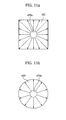
- FIGS. 11a and 11b are schematic comparative diagrams in which a current flows in an LED having a square upper surface and an LED having a round upper surface according to the fourth embodiment of the present invention.
- FIGS. 3a through 3e are cross-sectional views explaining a fabricating process of a high output LED according to a first embodiment of the present.
- a substrate (100) is sequentially stacked thereon with an N-type semiconductor layer (110), an active layer (120), and a P-type semiconductor layer (130) (FIG.3a), and mesa-etching is carried out from the P-type semiconductor layer (130) to portions of the N-type semiconductor layer (110) so that the sidewall thereof is inclined (FIG.3b).
- the sidewall is etched at a predetermined angle ( ⁇ 1).
- a mask layer is formed on the upper surface of the P-type semiconductor (130) except for a region to be etched, and the P-type semiconductor (130) is masked by the mask layer and dry-etched to obtain an inclined sidewall.
- the inclined angle ( ⁇ 2) of the remaining sidewall may be the same as the angle ( ⁇ 1) of the mesa-etched sidewall, or may be different.
- the inclined angles ( ⁇ 1 and ⁇ 2) are in the range of 30 ⁇ 70 degrees.
- the inclined sidewall is evaporated with a reflective film (140) (FIG.3d).
- the inclined sidewall facilitates the evaporation of the reflective film (140).
- the reflective film (140) is an anti-reflection (AR) film, a film stacked with reflective layers, or a high reflection (HR) film.
- the HR film is an insulating film having high reflection, and serves per se to reflect the light emitted from a sidewall of an LED and functions to passivate the device as well.
- the AR film per se is an insulating film having a high transmission factor.
- the AR film does not act as a reflective film, it functions as an excellent reflective material and serves to protect the device if formed with a reflective film at an external side thereof because it has a high optical transmission factor.
- the reflective film is made of metal such as Ag or Al.
- the N electrode (150) is formed on the mesa-etched N-type semiconductor layer (110) and the P electrode (160) is formed on the P-type semiconductor layer (FIG.3e).
- the afore-mentioned process enables to fabricate an LED according to the first embodiment of the present invention.
- FIG. 4 is a mimetic cross-sectional view illustrating and explaining a state where the high output LED according to the first embodiment of the present invention is bonded to a reflective plate to emit light.
- the high output LED is formed in such a manner that a substrate (100) is sequentially stacked thereon with an N-type semiconductor layer (110), an active layer (120) and a P-type semiconductor layer (130), mesa-etching is performed from the P-type semiconductor layer (130) to portions of the N-type semiconductor layer (110), a mesa-etched sidewall and sidewalls of the P-type semiconductor layer (130), the active layer (120) and N-type semiconductor layer (110) are all inclined, the inclined sidewalls are formed with a reflective film (140), an N electrode (150) is formed on the mesa-etched N-type semiconductor layer (110), and a P electrode (160) is formed on the P-type semiconductor layer (130).
- the LED (170) thus fabricated is bonded to an upper surface of a reflective plate (190) by bonding material (180).
- the light emitted from the active layer (120) is reflected by the reflective film (140) formed at a sidewall of the LED to be emitted upward of the P-type semiconductor layer (130) of the device. Consequently, the light is not irradiated to the sidewall but advances straight to the upward of the device, enabling to improve the light output.
- FIGS. 5a through 5e are cross-sectional views illustrating a fabricating process of a high output LED according to a second embodiment of the present invention.
- a substrate (200) is sequentially stacked with an N-type semiconductor layer (210), an active layer (220) and a P-type semiconductor layer (230) (FIG.5a). Etching is carried out from the P-type semiconductor layer (230) to the N-type semiconductor layer (210) to form an etched sidewall (FIG.5b). The etched sidewall has a predetermined angle ( ⁇ 3).
- the substrate (200) is detached from the N-type semiconductor layer (210) (FIG.5c).
- the P-type semiconductor layer (230) is formed thereunder with a reflecting P electrode (240) (FIG.5d).
- the inclined sidewall is formed with a reflective film (250) and the N-type semiconductor layer (210) is formed thereon with an N electrode (260) (FIG.5e).
- a width (W1) of the P-type semiconductor layer (230) is smaller than a width (W2) of the N-type semiconductor layer (210).
- FIG.6 is a mimetic cross-sectional view explaining a state where light is emitted from the high output LED according to the second embodiment of the present invention.
- the high output LED according to the second embodiment of the present invention fabricated by the process illustrated in FIGS. 5a through 5e is formed in such a manner that a P-type semiconductor layer (230) is sequentially stacked thereon with an active layer (220) and an N-type semiconductor layer, sidewalls of the P-type, semiconductor layer (230), the active layer (220) and the N-type semiconductor layer are inclined, the inclined sidewalls are formed with a reflective film (250), the P-type semiconductor layer (230) is formed thereunder with a reflective P electrode (240) and the N-type semiconductor layer is formed thereon with an N electrode.
- the light emitted from the active layer (220) is reflected from the reflective film (250) formed on a sidewall of the LED and the reflective N electrode (240) and emitted to the outside of the N-type semiconductor layer (210) on the device.
- the light is not emitted to the sidewall in the LED of the second embodiment of the present invention, and the light advances straight and is emitted upward of the device, enabling to improve the light output.
- FIGS. 7a and 7b are perspective views explaining a fabricating process of a high output LED according to a third embodiment of the present invention.
- a substrate (300) is sequentially stacked thereon with a N-type semiconductor layer (310), an active layer (320) and a P-type semiconductor layer (330), and the P-type semiconductor layer (330) is formed thereon with a mask layer (340) formed at a sidewall thereof with indents (341) (FIG.7a).
- the P-type semiconductor layer (330) is masked by the mask layer (340), and etching is carried out from the P-type semiconductor layer (330) to the N-type semiconductor layer (310).
- the etched sidewall is formed with inclinations and indents (FIG. 7b).
- the substrate (300) is detached from the N-type semiconductor layer (310).
- the reflective P electrode is formed under or underneath the P-type semiconductor layer (330).
- the inclined sidewall is formed with a reflective film and N electrode is formed on the N-type semiconductor layer (310).
- the sidewall of the light emitting structure is formed with indents to allow the sidewall of the active layer to be also formed with indents, thereby increasing the light emitting area.
- FIGS. 8a and 8b are plan views of an example of a mask layer according to aspects relating to a third embodiment of the present invention.
- the mask layer is a square layer or a layer whose margin is interjected with removed regions each spaced at a predetermined distance apart.
- the mask layer is a square layer or a layer, one margin of which is removed of a region.
- the mask layer may be multi-angled, or formed at a marginal sidewall thereof with indents combined of plain or curved surfaces.
- the indents of the sidewalls of the LED formed by use of the mask may be formed with plain surface and curved surface.
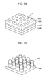
- FIGS. 9a and 9b are perspective views explaining a fabricating process of a high output LED according to a fourth embodiment of the present invention.
- a substrate (400) is sequentially stacked with a N-type semiconductor layer (410), an active layer. (420) and a P-type semiconductor layer (430).
- the P-type semiconductor layer (430) is formed thereon with a plurality of disc-shaped mask layers (440) each spaced a predetermined distance apart (FIG.9a).
- the P-type semiconductor layer (430) is masked by the mask layer (440) and etching is executed from the P-type semiconductor layer (430) to the N-type semiconductor layer (410).
- the etched sidewall is formed with an inclination (FIG.9b).
- the substrate (400) may be formed thereon with a plurality of cylindrical light emitting structures, each structure having a wider lower portion and a smaller upper portion.
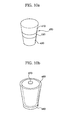
- FIGS. 10a and 10b are perspective views explaining a process of forming an electrode and a reflective film on each LED according to the fourth embodiment of the present invention.
- the substrate (400) is detached from the N-type semiconductor layer (410), and reversely positioned to obtain a light emitting structure (450) stacked with the P-type semiconductor layer (430), the active layer (420) and the N-type semiconductor layer (410) as illustrated in FIG.10a.
- the light emitting structure (450) has a cylindrical shape where a diameter of the P-type semiconductor layer (430) is smaller than that of the N-type semiconductor layer (410).
- a sidewall of the light emitting structure (450) is formed with a reflective film (480).
- a lower portion of the P-type semiconductor layer (460) is formed with a P electrode (460) and an upper portion of the N-type semiconductor layer (410) is formed with an N electrode (470).
- the cylindrical LED can allow the current to flow uniformly to make the light strength on a light emitting surface even such that color sensitivity becomes excellent when an LED is applied to a light source and a display.
- FIGS. 11a and 11b are schematic comparative diagrams in which a current flows in an LED having a square upper surface and an LED having a round upper surface according to aspects relating to the fourth embodiment of the present invention.
- An LED having a square upper surface as shown in FIG.11 a allows each distance of a current reaching from the P electrode (470a) to a margin of the P-type semiconductor layer (431) to differ, resulting in an uneven light strength. Meanwhile, an LED having a round upper surface as illustrated in FIG.11b allows each distance of a current reaching from the P electrode to a margin of the P-type semiconductor layer (430) to be identical, resulting in an even light strength.
- the LED according to the fourth embodiment of the present invention enables the light strength from a light emitting surface to be even.
- a sidewall of an LED is inclined and a reflective film is formed on the inclined sidewall to allow light emitted outside of the sidewall to reflect from the reflective film and to emit upward of the device, thereby enabling to improve a light output and dispensing with an additional passivation process.
- Another advantage is that indents are formed on a sidewall of a light emitting structure to thereby increase a light emitting surface and to improve a light output.
- Still another advantage is that a cylindrical LED is embodied to allow light from a light emitting surface to be emitted in an even strength by flowing current uniformly.
Abstract
Description
- This application claims the benefit of Korean Patent Application No. 2004-0117766, filed on December 31, 2004, which is hereby incorporated by reference for all purposes as if fully set forth herein.
- The present invention relates to a high output light emitting diode (LED) and a method for fabricating the same wherein a sidewall of the LED is inclined and a reflective film is formed on the inclined sidewall to allow light emitted outside of the sidewall to reflect from the reflective film and to emit upward of the device, thereby enabling to improve a light output and dispensing with an additional passivation process.
- Generally, an LED is widely used in applied fields such as color bulletin boards, traffic lights, keypad light sources for mobile telephones, light sources for illumination and LCD backlights.
- FIG.1 is a cross-sectional view of a conventional LED. The LED includes a substrate (10) sequentially stacked thereon with an N-type semiconductor layer (11), an active layer (12) and a P-type semiconductor layer (13), mesa etched from the P-type semiconductor layer (13) to portions of the N-type semiconductor layer (11), a transparent electrode (14) formed on the P-type semiconductor layer (13), an N electrode (15) formed on the mesa-etched N-type semiconductor layer (11) and a P electrode (16) formed on the transparent electrode (14).
- If current flows in the N electrode (15) and the P electrode (16) in the LED, light is generated from the active layer (12) and emitted outside of the device. Many attempts have been made to increase the light output of the LED, and a device manufacturing of flip chip structure is one of the attempts.
- FIG.2 is a mimetic cross-sectional view of a flip chip LED bonded to a sub mount substrate according to the prior art. Referring to the LED structure of FIG.1, the flip chip LED is structured in such a manner that the P-type semiconductor layer (13) is stacked thereon with a reflective film (16) for P electrode, the reflective film (16) and the N electrode (15) are bonded to a sub mount substrate (30) by conductive bonding materials such as solders (20a. 20b), and light is emitted toward the substrate (10).
- In other words, the flip chip type light device is such that the light emitted from the active layer (12) is reflected from the reflective film (16) to be emitted outside of the device via the substrate (10).
- However, the light emitted from the flip chip type light device is reflected from an entire surface of the device to the disadvantage of wasting the light emitted from the sidewall of the device.
- Particularly, in the case of a cleavage plane of the device, part of light emitted from a sidewall of the device is reflected from the cleavage plane, confined inside the device and cannot be emitted therefrom, thereby resulting in decreased light emission from the device.
- The present invention is directed to solve the afore-mentioned problems, and it is an object of the invention to provide a high output LED and a method for fabricating the same wherein a sidewall of the LED is inclined and a reflective film is formed on the inclined sidewall to allow light emitted outside of the sidewall to reflect from the reflective film and to emit upward of the device, thereby enabling to improve a light output and dispensing with an additional passivation process.
- Another object of the invention is to form a curvature on a sidewall of a light emitting structure to increase a light emitting area and to improve a light output.
- Still another object is to create a cylindrical LED and to uniformly pass current, thereby enabling light emitted from a light emitting surface to be outputted in a uniform strength.
- In a first aspect of the invention, a high output LED comprising a structure sequentially stacked with an N-type semiconductor layer, an active layer and a P-type semiconductor layer to allow the light emitted from the active layer, is formed in such a manner that a front surface of a sidewall of the structure stacked with the N-type semiconductor layer, the active layer and the P-type semiconductor layer is inclined, and a reflective film is formed at an entire inclined sidewall for reflecting light emitted from the active layer.
- In a second aspect of the invention, a high output LED is formed in such a manner that a substrate is sequentially stacked thereon with an N-type semiconductor layer, an active layer and a P-type semiconductor layer, mesa-etching is performed from the P-type semiconductor layer to portions of the N-type semiconductor layer, a mesa-etched sidewall and sidewalls of the P-type semiconductor layer, the active layer and N-type semiconductor layer are all inclined, the inclined sidewalls are formed with a reflective film, an N electrode is formed on the mesa-etched N-type semiconductor layer, and a P electrode is formed on the P-type semiconductor layer.
- In a third aspect of the invention, a high output LED is formed in such a manner that an active layer and a N-type semiconductor layer are sequentially stacked on a P-type semiconductor layer, sidewalls of the P-type semiconductor layer, the active layer and the N-type semiconductor layer are inclined, the inclined sidewalls are formed with reflective films, and the N-type semiconductor layer is formed thereon with an N electrode.
- In a fourth aspect of the invention, a method for fabricating a high output LED comprising: sequentially stacking an N-type semiconductor layer, an active layer and a P-type semiconductor layer on a substrate; mesa-etching in such a manner that mesa-etched sidewalls from the P-type semiconductor layer to portions of the N-type semiconductor layer are inclined; etching the remaining sidewalls of the N-type semiconductor, the active layer and the P-type semiconductor layer except for the mesa-etched portions to form inclined sidewalls; evaporating reflective films on the inclined sidewalls; and forming an N electrode on the mesa-etched N-type semiconductor layer, and forming a P electrode on the P-type semiconductor layer.
- In a fifth aspect of the invention, a method for fabricating a high output LED comprising: sequentially stacking an N-type semiconductor layer, an active layer and a P-type semiconductor layer on a substrate; etching from the P-type semiconductor layer to portions of the N-type semiconductor layer and forming an inclination on the etched sidewalls; detaching the substrate from the N-type semiconductor layer; forming a reflecting P electrode underneath the P-type semiconductor layer; and forming a reflective film on the inclined sidewalls and forming an N electrode on the N-type semiconductor layer.
- In a sixth aspect of the invention, a method for fabricating a high output LED comprising: sequentially stacking an N-type semiconductor layer, an active layer and a P-type semiconductor layer on a substrate; forming a mask layer formed with a curvature on a sidewall on an upper surface of the P-type semiconductor layer; masking the P-type semiconductor by the masking layer and etching from the P-type semiconductor layer to the N-type semiconductor layer to form an inclination and indents on the etched sidewalls; detaching the substrate from the N-type semiconductor layer; forming a reflecting P electrode underneath the P-type semiconductor layer; and forming a reflective film on the inclined sidewalls; and forming an N electrode on the N-type semiconductor layer.
- In a seventh aspect of the invention, a method for fabricating a high output LED comprising: sequentially stacking an N-type semiconductor layer, an active layer and a P-type semiconductor layer on a substrate; forming on the P-type semiconductor layer a plurality of disc-shaped mask layers, each mask layer spaced a predetermined distance apart; masking the P-type semiconductor layer by the plurality of mask layers and etching from the P-type semiconductor layer to the N-type semiconductor layer to form an inclination on the etched sidewalls; detaching the substrate from the N-type semiconductor layer to obtain a plurality of light emitting structures on which a P-type semiconductor layer, an active layer and an N-type semiconductor layer are stacked; forming reflective films on each sidewall of the light emitting structures; forming N electrodes underneath each N-type semiconductor layer of the light emitting structures; and forming P electrodes on each P-type semiconductor layer of the light emitting structures.
- FIG.1 is a cross-sectional view of an LED according to the prior art.
- FIG.2 is a mimetic cross-sectional view of a flip chip LED bonded to a sub mount substrate according to the prior art.
- FIGS. 3a, 3b, 3c, 3d, and 3e are cross-sectional views illustrating and explaining a fabricating process of a high output LED according to a first embodiment of the present.
- FIG. 4 is a mimetic cross-sectional view illustrating and explaining a state where the high output LED according to the first embodiment of the present invention is bonded to a reflective plate to emit light.
- FIGS. 5a, 5b, 5c, 5d and 5e are cross-sectional views illustrating and explaining a fabricating process of a high output LED according to a second embodiment of the present invention.
- FIG. 6 is a mimetic cross-sectional view illustrating and explaining a state where light is emitted from the high output LED according to the second embodiment of the present invention.
- FIGS. 7a and 7b are perspective views explaining a fabricating process of a high output LED according to a third embodiment of the present invention.
- FIGS. 8a and 8b are plan views of examples of mask layers according to the third embodiment of the present invention.
- FIGS. 9a and 9b are perspective views explaining a fabricating process of a high output LED according to a fourth embodiment of the present invention.
- FIGS. 10a and 10b are perspective views explaining a process of forming an electrode and a reflective film on each LED according to the fourth embodiment of the present invention.
- FIGS. 11a and 11b are schematic comparative diagrams in which a current flows in an LED having a square upper surface and an LED having a round upper surface according to the fourth embodiment of the present invention.
- FIGS. 3a through 3e are cross-sectional views explaining a fabricating process of a high output LED according to a first embodiment of the present.
- A substrate (100) is sequentially stacked thereon with an N-type semiconductor layer (110), an active layer (120), and a P-type semiconductor layer (130) (FIG.3a), and mesa-etching is carried out from the P-type semiconductor layer (130) to portions of the N-type semiconductor layer (110) so that the sidewall thereof is inclined (FIG.3b).
- In other words, in the process of FIG. 3b, the sidewall is etched at a predetermined angle (α1).
- In order to etch the sidewall having an inclination, a mask layer is formed on the upper surface of the P-type semiconductor (130) except for a region to be etched, and the P-type semiconductor (130) is masked by the mask layer and dry-etched to obtain an inclined sidewall.
- Successively, remaining sidewall of the N-type semiconductor layer (110), the active layer (120) and the P-type semiconductor layer (130) except for the mesa-etched region is etched to form an inclined sidewall (FIG.3c).
- At this time, the inclined angle (α2) of the remaining sidewall may be the same as the angle (α1) of the mesa-etched sidewall, or may be different. Preferably, the inclined angles (α1 and α2) are in the range of 30~70 degrees.
- Then, the inclined sidewall is evaporated with a reflective film (140) (FIG.3d). The inclined sidewall facilitates the evaporation of the reflective film (140). Preferably, the reflective film (140) is an anti-reflection (AR) film, a film stacked with reflective layers, or a high reflection (HR) film.
- The HR film is an insulating film having high reflection, and serves per se to reflect the light emitted from a sidewall of an LED and functions to passivate the device as well.
- Furthermore, the AR film per se is an insulating film having a high transmission factor. Although the AR film does not act as a reflective film, it functions as an excellent reflective material and serves to protect the device if formed with a reflective film at an external side thereof because it has a high optical transmission factor.
- Preferably, the reflective film is made of metal such as Ag or Al.
- As a last step, the N electrode (150) is formed on the mesa-etched N-type semiconductor layer (110) and the P electrode (160) is formed on the P-type semiconductor layer (FIG.3e). As illustrated in FIG.3e, the afore-mentioned process enables to fabricate an LED according to the first embodiment of the present invention.
- FIG. 4 is a mimetic cross-sectional view illustrating and explaining a state where the high output LED according to the first embodiment of the present invention is bonded to a reflective plate to emit light.
- The high output LED according to the first embodiment of the present invention fabricated via the processes from FIG.3a through 3e, the high output LED is formed in such a manner that a substrate (100) is sequentially stacked thereon with an N-type semiconductor layer (110), an active layer (120) and a P-type semiconductor layer (130), mesa-etching is performed from the P-type semiconductor layer (130) to portions of the N-type semiconductor layer (110), a mesa-etched sidewall and sidewalls of the P-type semiconductor layer (130), the active layer (120) and N-type semiconductor layer (110) are all inclined, the inclined sidewalls are formed with a reflective film (140), an N electrode (150) is formed on the mesa-etched N-type semiconductor layer (110), and a P electrode (160) is formed on the P-type semiconductor layer (130).
- The LED (170) thus fabricated is bonded to an upper surface of a reflective plate (190) by bonding material (180). The light emitted from the active layer (120) is reflected by the reflective film (140) formed at a sidewall of the LED to be emitted upward of the P-type semiconductor layer (130) of the device. Consequently, the light is not irradiated to the sidewall but advances straight to the upward of the device, enabling to improve the light output.
- FIGS. 5a through 5e are cross-sectional views illustrating a fabricating process of a high output LED according to a second embodiment of the present invention.
- A substrate (200) is sequentially stacked with an N-type semiconductor layer (210), an active layer (220) and a P-type semiconductor layer (230) (FIG.5a). Etching is carried out from the P-type semiconductor layer (230) to the N-type semiconductor layer (210) to form an etched sidewall (FIG.5b). The etched sidewall has a predetermined angle (α3). The substrate (200) is detached from the N-type semiconductor layer (210) (FIG.5c). Successively, the P-type semiconductor layer (230) is formed thereunder with a reflecting P electrode (240) (FIG.5d). The inclined sidewall is formed with a reflective film (250) and the N-type semiconductor layer (210) is formed thereon with an N electrode (260) (FIG.5e). Preferably, a width (W1) of the P-type semiconductor layer (230) is smaller than a width (W2) of the N-type semiconductor layer (210).
- FIG.6 is a mimetic cross-sectional view explaining a state where light is emitted from the high output LED according to the second embodiment of the present invention.
- The high output LED according to the second embodiment of the present invention fabricated by the process illustrated in FIGS. 5a through 5e is formed in such a manner that a P-type semiconductor layer (230) is sequentially stacked thereon with an active layer (220) and an N-type semiconductor layer, sidewalls of the P-type, semiconductor layer (230), the active layer (220) and the N-type semiconductor layer are inclined, the inclined sidewalls are formed with a reflective film (250), the P-type semiconductor layer (230) is formed thereunder with a reflective P electrode (240) and the N-type semiconductor layer is formed thereon with an N electrode.
- In the LED thus constructed, the light emitted from the active layer (220) is reflected from the reflective film (250) formed on a sidewall of the LED and the reflective N electrode (240) and emitted to the outside of the N-type semiconductor layer (210) on the device.
- Consequently, the light is not emitted to the sidewall in the LED of the second embodiment of the present invention, and the light advances straight and is emitted upward of the device, enabling to improve the light output.
- FIGS. 7a and 7b are perspective views explaining a fabricating process of a high output LED according to a third embodiment of the present invention.
- A substrate (300) is sequentially stacked thereon with a N-type semiconductor layer (310), an active layer (320) and a P-type semiconductor layer (330), and the P-type semiconductor layer (330) is formed thereon with a mask layer (340) formed at a sidewall thereof with indents (341) (FIG.7a).
- The P-type semiconductor layer (330) is masked by the mask layer (340), and etching is carried out from the P-type semiconductor layer (330) to the N-type semiconductor layer (310). The etched sidewall is formed with inclinations and indents (FIG. 7b).
- Successively, the substrate (300) is detached from the N-type semiconductor layer (310). The reflective P electrode is formed under or underneath the P-type semiconductor layer (330). The inclined sidewall is formed with a reflective film and N electrode is formed on the N-type semiconductor layer (310).
- There is an advantage in the high output LED thus fabricated according to the third embodiment of the present invention in that the inclined sidewall is formed with indents to increase a light emitting area and a light output.
- In other words, the sidewall of the light emitting structure is formed with indents to allow the sidewall of the active layer to be also formed with indents, thereby increasing the light emitting area.
- FIGS. 8a and 8b are plan views of an example of a mask layer according to aspects relating to a third embodiment of the present invention.
- Referring to FIG.8a, the mask layer is a square layer or a layer whose margin is interjected with removed regions each spaced at a predetermined distance apart. Referring to FIG.8b, the mask layer is a square layer or a layer, one margin of which is removed of a region.
- The mask layer may be multi-angled, or formed at a marginal sidewall thereof with indents combined of plain or curved surfaces. The indents of the sidewalls of the LED formed by use of the mask may be formed with plain surface and curved surface.
- FIGS. 9a and 9b are perspective views explaining a fabricating process of a high output LED according to a fourth embodiment of the present invention.
- A substrate (400) is sequentially stacked with a N-type semiconductor layer (410), an active layer. (420) and a P-type semiconductor layer (430). The P-type semiconductor layer (430) is formed thereon with a plurality of disc-shaped mask layers (440) each spaced a predetermined distance apart (FIG.9a).
- Successively, the P-type semiconductor layer (430) is masked by the mask layer (440) and etching is executed from the P-type semiconductor layer (430) to the N-type semiconductor layer (410). The etched sidewall is formed with an inclination (FIG.9b).
- By the process thus described according to FIG.9b, the substrate (400) may be formed thereon with a plurality of cylindrical light emitting structures, each structure having a wider lower portion and a smaller upper portion.
- FIGS. 10a and 10b are perspective views explaining a process of forming an electrode and a reflective film on each LED according to the fourth embodiment of the present invention.
- Following the process of FIG.9b, the substrate (400) is detached from the N-type semiconductor layer (410), and reversely positioned to obtain a light emitting structure (450) stacked with the P-type semiconductor layer (430), the active layer (420) and the N-type semiconductor layer (410) as illustrated in FIG.10a.
- The light emitting structure (450) has a cylindrical shape where a diameter of the P-type semiconductor layer (430) is smaller than that of the N-type semiconductor layer (410).
- Now, referring to FIG.10b, a sidewall of the light emitting structure (450) is formed with a reflective film (480). A lower portion of the P-type semiconductor layer (460) is formed with a P electrode (460) and an upper portion of the N-type semiconductor layer (410) is formed with an N electrode (470).
- This process completes a fabrication of a cylindrical LED. The cylindrical LED can allow the current to flow uniformly to make the light strength on a light emitting surface even such that color sensitivity becomes excellent when an LED is applied to a light source and a display.
- FIGS. 11a and 11b are schematic comparative diagrams in which a current flows in an LED having a square upper surface and an LED having a round upper surface according to aspects relating to the fourth embodiment of the present invention.
- An LED having a square upper surface as shown in FIG.11 a allows each distance of a current reaching from the P electrode (470a) to a margin of the P-type semiconductor layer (431) to differ, resulting in an uneven light strength. Meanwhile, an LED having a round upper surface as illustrated in FIG.11b allows each distance of a current reaching from the P electrode to a margin of the P-type semiconductor layer (430) to be identical, resulting in an even light strength.
- Consequently, the LED according to the fourth embodiment of the present invention enables the light strength from a light emitting surface to be even.
- As apparent from the foregoing, there is an advantage in the preferred embodiments of the present invention thus described in that a sidewall of an LED is inclined and a reflective film is formed on the inclined sidewall to allow light emitted outside of the sidewall to reflect from the reflective film and to emit upward of the device, thereby enabling to improve a light output and dispensing with an additional passivation process.
- Another advantage is that indents are formed on a sidewall of a light emitting structure to thereby increase a light emitting surface and to improve a light output.
- Still another advantage is that a cylindrical LED is embodied to allow light from a light emitting surface to be emitted in an even strength by flowing current uniformly.
- The present invention has been described above in varied detail by reference to particular exemplary embodiments and figures. Those skilled in the art will readily observe that numerous modifications and alterations of the invention may be made while retaining the teachings of the invention. Accordingly, the above disclosure should be construed as limited only by the metes and bounds of appended claims.
Claims (19)
- A high output light emitting diode (LED) comprising:a structure having an inclined surface that includes an N-type semiconductor layer, an active layer and a P-type semiconductor layer; anda reflective film disposed along substantially all of the inclined surface to reflect light emitted from the active layer;wherein the N-type semiconductor layer, the active layer, and the P-type semiconductor layer are provided in a stack, said stack being configured to allow light to be emitted from the active layer.
- The LED as defined in claim 1, further comprising an angle defined by the inclined sidewall, the angle being in a range of 30~70 degrees.
- The LED as defined in claim 1, wherein the reflective film comprises an anti-reflection (AR) film, a film stacked with reflective layers, or a high-reflection (HR) film.
- A high output light emitting diode (LED) comprising:a stack including an N-type semiconductor layer, an active layer, and a P-type semiconductor layer, said stack including mesa-etched sidewalls from the P-type semiconductor layer to portions of the N-type semiconductor layer, wherein the mesa-etched sidewalls and sidewalls of the active layer are inclined;a reflective film disposed along the inclined sidewalls;an N electrode being disposed on the N-type semiconductor layer,a P electrode being disposed on the P-type semiconductor layer; anda substrate attached to the stack.
- The LED as defined in claim 4, wherein the inclined sidewalls comprise indents.
- A high output LED comprises:a structure including an active layer, an N-type semiconductor layer, and a P-type semiconductor layer, wherein the P-type semiconductor layer, the active layer and the N-type semiconductor layer include inclined sidewalls;reflective films being disposed along the inclined sidewalls; andan N electrode being disposed on the N-type semiconductor layer.
- The LED as defined in claim 6, wherein the inclined sidewalls comprise indents.
- The LED as defined in claim 7, wherein the indents comprise planar portions and curved portions.
- The LED as defined in claim 6, wherein the P-type semiconductor layer, the active layer and the N-type semiconductor layer are configured in a stack such that a diameter of the P-type semiconductor layer is smaller than a diameter of the N-type semiconductor layer.
- A method for fabricating a high output LED comprising:stacking an N-type semiconductor layer, an active layer and a P-type semiconductor layer on a substrate;mesa-etching sidewalls to be inclined from the P-type semiconductor layer to portions of the N-type semiconductor layer;etching remaining sidewalls of the N-type semiconductor, the active layer, and the P-type semiconductor layer except for the mesa-etched sidewalls to be inclined; evaporating reflective films on the inclined sidewalls; andforming an N electrode on the mesa-etched N-type semiconductor layer, and forming a P electrode on the P-type semiconductor layer.
- The method as defined in claim 10, wherein an inclination of the inclined sidewalls is in a range of 30~70 degrees.
- The method as defined in claim 10, wherein the reflective film is an ant-reflection (AR) film, a film stacked with reflective layers, or a high-reflection (HR) film.
- A method for fabricating a high output LED comprising:stacking an N-type semiconductor layer, an active layer and a P-type semiconductor layer on a substrate;etching sidewalls from the P-type semiconductor layer to portions of the N-type semiconductor layer;forming an inclination on the etched sidewalls;detaching the substrate from the N-type semiconductor layer;forming a reflecting P electrode under the P-type semiconductor layer; andforming a reflective film on the inclined sidewalls and forming an N electrode on the N-type semiconductor layer.
- The method as defined in claim 13, wherein the inclination is in a range of 30∼70 degrees.
- The method as defined in claim 13, wherein the reflective film is an anti-reflection (AR) film, a film stacked with reflective layers, or a high-reflection (HR) film.
- A method for fabricating a high output LED comprising:stacking an N-type semiconductor layer, an active layer and a P-type semiconductor layer on a substrate;forming a mask layer with a curvature on a sidewall of an upper surface of the P-type semiconductor layer;masking the P-type semiconductor with the mask layer and etching from the P-type semiconductor layer to the N-type semiconductor layer to create inclinations and indents on sidewalls of the stack;detaching the substrate from the N-type semiconductor layer;forming a reflecting P electrode under the P-type semiconductor layer;forming a reflective film on the inclined sidewalls; andforming an N electrode on the N-type semiconductor layer.
- The method as defined in claim 16, wherein the mask layer includes a marginal sidewall with indents comprising planar or curved portions.
- A method for fabricating a high output LED comprising:stacking an N-type semiconductor layer, an active layer, and a P-type semiconductor layer on a substrate;forming a plurality of disc-shaped mask layers on the P-type semiconductor layer, each disc-shaped mask layer being spaced a predetermined distance apart;masking the P-type semiconductor layer by the plurality of mask layers and etching from the P-type semiconductor layer to the N-type semiconductor layer to create an inclination on sidewalls of the stack;detaching the substrate from the N-type semiconductor layer to obtain a plurality of light emitting structures that includes the P-type semiconductor layer, the active layer and the N-type semiconductor layer;forming reflective films on side surfaces of the light emitting structures;forming N electrodes adjacent to each N-type semiconductor layer of the light emitting structures; andforming P electrodes adjacent to each P-type semiconductor layer of the light emitting structures.
- The method as defined in claim 18, wherein the light emitting structure comprises a diameter of the P-type semiconductor layer that is smaller than a diameter of the N-type semiconductor layer.
Applications Claiming Priority (1)
| Application Number | Priority Date | Filing Date | Title |
|---|---|---|---|
| KR1020040117766A KR20060077801A (en) | 2004-12-31 | 2004-12-31 | High output light emitting diode and method for fabricating the same |
Publications (3)
| Publication Number | Publication Date |
|---|---|
| EP1677366A2 true EP1677366A2 (en) | 2006-07-05 |
| EP1677366A3 EP1677366A3 (en) | 2007-04-11 |
| EP1677366B1 EP1677366B1 (en) | 2012-02-01 |
Family
ID=36129689
Family Applications (1)
| Application Number | Title | Priority Date | Filing Date |
|---|---|---|---|
| EP05292775A Not-in-force EP1677366B1 (en) | 2004-12-31 | 2005-12-22 | High output light emitting diode and method for fabricating the same |
Country Status (5)
| Country | Link |
|---|---|
| US (1) | US7939841B2 (en) |
| EP (1) | EP1677366B1 (en) |
| JP (1) | JP4721166B2 (en) |
| KR (1) | KR20060077801A (en) |
| CN (1) | CN100517777C (en) |
Cited By (10)
| Publication number | Priority date | Publication date | Assignee | Title |
|---|---|---|---|---|
| DE102006041460A1 (en) * | 2006-09-04 | 2008-03-13 | Osram Opto Semiconductors Gmbh | Radiation emitting semiconductor chip, has semiconductor layer sequence with active area for producing electromagnetic radiation, which is arranged between base and side surfaces, and reflecting layer is applied on base and side surfaces |
| US20090321770A1 (en) * | 2008-06-25 | 2009-12-31 | Shuichi Ajiki | Semiconductor Light-Emitting Device |
| EP2311108A2 (en) * | 2008-09-30 | 2011-04-20 | LG Innotek Co., Ltd | Semiconductor light emitting device and method of manufacturing the same |
| US8476666B2 (en) | 2008-06-24 | 2013-07-02 | Samsung Electronics Co., Ltd. | Light emitting elements, light emitting devices including light emitting elements and methods of manufacturing such light emitting elements and/or devices |
| EP2390931A3 (en) * | 2010-05-24 | 2014-04-30 | LG Innotek Co., Ltd. | Light emitting device, light emitting device package, and lighting device system |
| CN108269885A (en) * | 2016-12-30 | 2018-07-10 | 晶能光电(江西)有限公司 | A kind of single side light extracting LED chip preparation method |
| US10121864B2 (en) | 2011-11-18 | 2018-11-06 | Apple Inc. | Micro device transfer head heater assembly and method of transferring a micro device |
| US10297712B2 (en) | 2011-11-18 | 2019-05-21 | Apple Inc. | Micro LED display |
| EP2495761B1 (en) * | 2011-03-01 | 2019-06-19 | Sony Corporation | Light emitting unit and display device |
| EP4336575A1 (en) * | 2022-09-07 | 2024-03-13 | Samsung Display Co., Ltd. | Light-emitting element and display device including the same |
Families Citing this family (56)
| Publication number | Priority date | Publication date | Assignee | Title |
|---|---|---|---|---|
| KR20080030404A (en) * | 2006-09-30 | 2008-04-04 | 서울옵토디바이스주식회사 | Method of fabricating light emitting diode chip |
| JP2009004625A (en) * | 2007-06-22 | 2009-01-08 | Sanken Electric Co Ltd | Semiconductor light emitting device |
| DE102007046519A1 (en) | 2007-09-28 | 2009-04-02 | Osram Opto Semiconductors Gmbh | Thin-film LED with a mirror layer and method for its production |
| CN101409315B (en) * | 2007-10-08 | 2011-07-20 | 杨文明 | Upside-down mounting LED chip |
| DE102009018603B9 (en) * | 2008-04-25 | 2021-01-14 | Samsung Electronics Co., Ltd. | Lighting device and manufacturing method thereof |
| CN101630706B (en) * | 2008-07-16 | 2011-02-16 | 玉晶光电股份有限公司 | Forward luminescent light-emitting diode structure |
| TW201017863A (en) * | 2008-10-03 | 2010-05-01 | Versitech Ltd | Semiconductor color-tunable broadband light sources and full-color microdisplays |
| KR100962898B1 (en) | 2008-11-14 | 2010-06-10 | 엘지이노텍 주식회사 | Semiconductor light emitting device and fabrication method thereof |
| USRE48774E1 (en) | 2008-11-14 | 2021-10-12 | Suzhou Lekin Semiconductor Co., Ltd. | Semiconductor light emitting device |
| KR101039100B1 (en) * | 2008-12-19 | 2011-06-07 | 주식회사 오디텍 | LED Package with Lens and Mirror |
| CN102376841A (en) * | 2008-12-22 | 2012-03-14 | 亿光电子工业股份有限公司 | Light-emitting diode structure and manufacturing method thereof |
| JP2010278274A (en) * | 2009-05-29 | 2010-12-09 | Sony Corp | Light emitting diode, and method of manufacturing the same |
| US8673662B2 (en) * | 2009-07-29 | 2014-03-18 | Tien-Tsai Lin | Light-emitting diode cutting method and product thereof |
| CN101740703B (en) * | 2009-11-30 | 2013-04-17 | 中微光电子(潍坊)有限公司 | LED chip and manufacturing method thereof |
| US9236532B2 (en) * | 2009-12-14 | 2016-01-12 | Seoul Viosys Co., Ltd. | Light emitting diode having electrode pads |
| KR101055768B1 (en) * | 2009-12-14 | 2011-08-11 | 서울옵토디바이스주식회사 | Light Emitting Diodes with Electrode Pads |
| KR101028327B1 (en) | 2010-04-15 | 2011-04-12 | 엘지이노텍 주식회사 | Light emitting device, fabrication method of light emitting device, and light emitting device package |
| CN101872824A (en) * | 2010-06-07 | 2010-10-27 | 厦门市三安光电科技有限公司 | Gallium nitride-based inverted light-emitting diode (LED) with two reflecting layers on lateral surfaces and preparation method thereof |
| CN102376838A (en) * | 2010-08-06 | 2012-03-14 | 隆达电子股份有限公司 | Light-emitting diode with region protection layer |
| CN102468394A (en) * | 2010-11-12 | 2012-05-23 | 佛山市奇明光电有限公司 | Light-emitting diode element and manufacturing method thereof |
| JP2012114377A (en) * | 2010-11-26 | 2012-06-14 | Mitsubishi Chemicals Corp | Semiconductor light-emitting element |
| EP2605295A3 (en) * | 2011-12-13 | 2015-11-11 | LG Innotek Co., Ltd. | Ultraviolet light emitting device |
| US9466768B2 (en) | 2012-01-13 | 2016-10-11 | Semicon Light Co., Ltd. | Semiconductor light emitting device with a light-reflecting face |
| US9548332B2 (en) * | 2012-04-27 | 2017-01-17 | Apple Inc. | Method of forming a micro LED device with self-aligned metallization stack |
| KR101420787B1 (en) * | 2012-12-04 | 2014-07-18 | 주식회사 세미콘라이트 | Semiconductor light emitting device and manufacturing method of the same |
| US9691944B2 (en) | 2012-12-04 | 2017-06-27 | Semicon Light Co., Ltd. | Semiconductor light-emitting device and method for manufacturing the same |
| US9536924B2 (en) | 2012-12-06 | 2017-01-03 | Seoul Viosys Co., Ltd. | Light-emitting diode and application therefor |
| CN110600593B (en) | 2012-12-06 | 2023-01-03 | 首尔伟傲世有限公司 | Light emitting diode |
| KR102006390B1 (en) | 2013-03-11 | 2019-08-01 | 삼성전자주식회사 | Method of manufacturing Light Emitting diode package |
| US9082926B2 (en) | 2013-06-18 | 2015-07-14 | Avago Technologies General Ip (Singapore) Pte. Ltd. | Semiconductor optical emitting device with metallized sidewalls |
| CN103367618B (en) * | 2013-07-19 | 2016-04-13 | 深圳大道半导体有限公司 | With the semiconductor luminous chip of reflection layer |
| CN103390713B (en) * | 2013-07-19 | 2016-04-13 | 深圳大道半导体有限公司 | With the light emitting semiconductor device of reflection layer |
| JP6215612B2 (en) * | 2013-08-07 | 2017-10-18 | ソニーセミコンダクタソリューションズ株式会社 | LIGHT EMITTING ELEMENT, LIGHT EMITTING ELEMENT WAFER, AND ELECTRONIC DEVICE |
| CN104821354A (en) * | 2015-05-07 | 2015-08-05 | 合肥彩虹蓝光科技有限公司 | Method for reducing light emitting angle of LED chip |
| KR102412409B1 (en) * | 2015-10-26 | 2022-06-23 | 엘지전자 주식회사 | Display device using semiconductor light emitting device and method for manufacturing the same |
| FR3044167B1 (en) * | 2015-11-20 | 2018-01-05 | Commissariat A L'energie Atomique Et Aux Energies Alternatives | OPTOELECTRONIC LIGHT EMITTING DIODE DEVICE COMPRISING AT LEAST ONE ZENER DIODE |
| JP7266961B2 (en) | 2015-12-31 | 2023-05-01 | 晶元光電股▲ふん▼有限公司 | light emitting device |
| CN105870284B (en) * | 2016-05-09 | 2018-09-14 | 青岛杰生电气有限公司 | Light emitting diode construction and its processing method |
| CN105977353B (en) * | 2016-05-11 | 2018-11-09 | 青岛杰生电气有限公司 | A kind of UV LED |
| JP6553541B2 (en) * | 2016-05-11 | 2019-07-31 | 日機装株式会社 | Deep UV light emitting element |
| CN105932120A (en) * | 2016-06-15 | 2016-09-07 | 佛山市国星半导体技术有限公司 | Manufacturing method of LED chip with side wall DBR |
| CN106129192B (en) * | 2016-07-19 | 2018-05-22 | 厦门乾照光电股份有限公司 | A kind of preparation process of isosceles trapezoid formula light emitting diode |
| CN107731982A (en) * | 2016-08-11 | 2018-02-23 | 晶能光电(江西)有限公司 | A kind of thin-film LED preparation method |
| CN106848029B (en) * | 2016-12-07 | 2019-06-11 | 华灿光电(浙江)有限公司 | A kind of chip of high-brightness light emitting diode and preparation method thereof |
| US10937928B2 (en) | 2017-11-09 | 2021-03-02 | Asahi Kasei Kabushiki Kaisha | Nitride semiconductor element, nitride semiconductor light emitting element, ultraviolet light emitting element |
| JP6822429B2 (en) * | 2018-02-19 | 2021-01-27 | 日亜化学工業株式会社 | Light emitting element |
| KR102136579B1 (en) * | 2018-07-27 | 2020-07-22 | 서울대학교산학협력단 | Display device |
| WO2020055061A1 (en) * | 2018-09-10 | 2020-03-19 | 주식회사 세미콘라이트 | Semiconductor light-emitting device and manufacturing method therefor |
| KR20200079122A (en) | 2018-12-24 | 2020-07-02 | 삼성전자주식회사 | Micro light emitting diode and manufacturing method of micro emitting diode |
| JP6902569B2 (en) | 2019-04-17 | 2021-07-14 | 日機装株式会社 | Semiconductor light emitting element and manufacturing method of semiconductor light emitting element |
| US20230096713A1 (en) * | 2020-02-21 | 2023-03-30 | Sony Semiconductor Solutions Corporation | Light-emiting element |
| KR102506449B1 (en) * | 2020-04-23 | 2023-03-07 | 삼성전자주식회사 | Display device |
| CN111640832A (en) * | 2020-06-18 | 2020-09-08 | 佛山紫熙慧众科技有限公司 | Ultraviolet light LED chip structure |
| CN113066914A (en) * | 2021-04-16 | 2021-07-02 | 厦门三安光电有限公司 | LED chip |
| US11870009B2 (en) * | 2021-08-06 | 2024-01-09 | Creeled, Inc. | Edge structures for light shaping in light-emitting diode chips |
| CN114038950A (en) * | 2021-08-09 | 2022-02-11 | 重庆康佳光电技术研究院有限公司 | Epitaxial layer etching method and LED chip |
Citations (2)
| Publication number | Priority date | Publication date | Assignee | Title |
|---|---|---|---|---|
| GB2311413A (en) | 1996-03-22 | 1997-09-24 | Hewlett Packard Co | Light emitting devices |
| US20010000209A1 (en) | 1997-06-03 | 2001-04-12 | Krames Michael R. | Led having angled sides for increased side light extraction |
Family Cites Families (18)
| Publication number | Priority date | Publication date | Assignee | Title |
|---|---|---|---|---|
| US3290539A (en) * | 1963-09-16 | 1966-12-06 | Rca Corp | Planar p-nu junction light source with reflector means to collimate the emitted light |
| JPS6476786A (en) * | 1987-09-17 | 1989-03-22 | Nec Corp | Semiconductor light-emitting diode and manufacture thereof |
| JP2818312B2 (en) * | 1990-04-18 | 1998-10-30 | 株式会社東芝 | Light emitting element |
| JPH05145118A (en) * | 1991-11-19 | 1993-06-11 | Mitsubishi Cable Ind Ltd | Light emitting device |
| JP2786375B2 (en) * | 1992-06-18 | 1998-08-13 | シャープ株式会社 | Light emitting diode |
| JPH0645650A (en) * | 1992-07-24 | 1994-02-18 | Omron Corp | Semiconductor light emittng element and optical detector, optical information processing device, and light emitting device using it |
| JPH06252440A (en) * | 1993-02-26 | 1994-09-09 | Kyocera Corp | Semiconductor light emitting device |
| JPH07307489A (en) * | 1994-05-13 | 1995-11-21 | Toshiba Corp | Semiconductor light-emitting element and its manufacture |
| JPH08139360A (en) * | 1994-09-12 | 1996-05-31 | Showa Denko Kk | Semiconductor hetero-junction material |
| JP2002043633A (en) * | 2000-07-25 | 2002-02-08 | Stanley Electric Co Ltd | White light emitting diode |
| US6630689B2 (en) * | 2001-05-09 | 2003-10-07 | Lumileds Lighting, U.S. Llc | Semiconductor LED flip-chip with high reflectivity dielectric coating on the mesa |
| JP2002344015A (en) * | 2001-05-17 | 2002-11-29 | Nichia Chem Ind Ltd | Nitride semiconductor light-emitting element |
| JP2004056010A (en) * | 2002-07-23 | 2004-02-19 | Toyota Central Res & Dev Lab Inc | Nitride semiconductor light emitting device |
| JP2004056034A (en) * | 2002-07-24 | 2004-02-19 | Sony Corp | Semiconductor light emitting element, and manufacturing method thereof |
| GB0302580D0 (en) * | 2003-02-05 | 2003-03-12 | Univ Strathclyde | MICRO LEDs |
| JP4212480B2 (en) | 2004-01-05 | 2009-01-21 | 日本メナード化粧品株式会社 | Cosmetics |
| JP4868709B2 (en) * | 2004-03-09 | 2012-02-01 | 三洋電機株式会社 | Light emitting element |
| JP2006128659A (en) * | 2004-09-29 | 2006-05-18 | Sumitomo Chemical Co Ltd | Nitride series semiconductor light emitting element and manufacturing method of the same |
-
2004
- 2004-12-31 KR KR1020040117766A patent/KR20060077801A/en active Search and Examination
-
2005
- 2005-12-22 EP EP05292775A patent/EP1677366B1/en not_active Not-in-force
- 2005-12-27 JP JP2005376038A patent/JP4721166B2/en not_active Expired - Fee Related
- 2005-12-28 US US11/318,505 patent/US7939841B2/en active Active
- 2005-12-29 CN CNB2005101329587A patent/CN100517777C/en not_active Expired - Fee Related
Patent Citations (2)
| Publication number | Priority date | Publication date | Assignee | Title |
|---|---|---|---|---|
| GB2311413A (en) | 1996-03-22 | 1997-09-24 | Hewlett Packard Co | Light emitting devices |
| US20010000209A1 (en) | 1997-06-03 | 2001-04-12 | Krames Michael R. | Led having angled sides for increased side light extraction |
Non-Patent Citations (1)
| Title |
|---|
| S. ILLEK ET AL.: "Scability of buried microreflector light-emitting diodes for high-current applications", LIGHT-EMITTING DIODES: RESEARCH, MANUFACTURING AND APPLICATIONS, vol. VII, 27 January 2003 (2003-01-27) |
Cited By (17)
| Publication number | Priority date | Publication date | Assignee | Title |
|---|---|---|---|---|
| DE102006041460A1 (en) * | 2006-09-04 | 2008-03-13 | Osram Opto Semiconductors Gmbh | Radiation emitting semiconductor chip, has semiconductor layer sequence with active area for producing electromagnetic radiation, which is arranged between base and side surfaces, and reflecting layer is applied on base and side surfaces |
| US8476666B2 (en) | 2008-06-24 | 2013-07-02 | Samsung Electronics Co., Ltd. | Light emitting elements, light emitting devices including light emitting elements and methods of manufacturing such light emitting elements and/or devices |
| US20090321770A1 (en) * | 2008-06-25 | 2009-12-31 | Shuichi Ajiki | Semiconductor Light-Emitting Device |
| US8258528B2 (en) * | 2008-06-25 | 2012-09-04 | Stanley Electric Co., Ltd. | Semiconductor light-emitting device |
| US8952414B2 (en) | 2008-09-30 | 2015-02-10 | Lg Innotek Co., Ltd. | Semiconductor light emitting device |
| EP2311108A2 (en) * | 2008-09-30 | 2011-04-20 | LG Innotek Co., Ltd | Semiconductor light emitting device and method of manufacturing the same |
| EP2311108A4 (en) * | 2008-09-30 | 2012-01-18 | Lg Innotek Co Ltd | Semiconductor light emitting device and method of manufacturing the same |
| US8188506B2 (en) | 2008-09-30 | 2012-05-29 | Lg Innotek Co., Ltd. | Semiconductor light emitting device |
| US8319249B2 (en) | 2008-09-30 | 2012-11-27 | Lg Innotek Co., Ltd. | Semiconductor light emitting device |
| EP2390931A3 (en) * | 2010-05-24 | 2014-04-30 | LG Innotek Co., Ltd. | Light emitting device, light emitting device package, and lighting device system |
| EP2495761B1 (en) * | 2011-03-01 | 2019-06-19 | Sony Corporation | Light emitting unit and display device |
| US10121864B2 (en) | 2011-11-18 | 2018-11-06 | Apple Inc. | Micro device transfer head heater assembly and method of transferring a micro device |
| US10297712B2 (en) | 2011-11-18 | 2019-05-21 | Apple Inc. | Micro LED display |
| US10607961B2 (en) | 2011-11-18 | 2020-03-31 | Apple Inc. | Micro device transfer head heater assembly and method of transferring a micro device |
| US11552046B2 (en) | 2011-11-18 | 2023-01-10 | Apple Inc. | Micro device transfer head assembly |
| CN108269885A (en) * | 2016-12-30 | 2018-07-10 | 晶能光电(江西)有限公司 | A kind of single side light extracting LED chip preparation method |
| EP4336575A1 (en) * | 2022-09-07 | 2024-03-13 | Samsung Display Co., Ltd. | Light-emitting element and display device including the same |
Also Published As
| Publication number | Publication date |
|---|---|
| KR20060077801A (en) | 2006-07-05 |
| JP2006191068A (en) | 2006-07-20 |
| CN100517777C (en) | 2009-07-22 |
| US20060145174A1 (en) | 2006-07-06 |
| JP4721166B2 (en) | 2011-07-13 |
| CN1822400A (en) | 2006-08-23 |
| EP1677366A3 (en) | 2007-04-11 |
| US7939841B2 (en) | 2011-05-10 |
| EP1677366B1 (en) | 2012-02-01 |
Similar Documents
| Publication | Publication Date | Title |
|---|---|---|
| EP1677366A2 (en) | High output light emitting diode and method for fabricating the same | |
| US7470938B2 (en) | Nitride semiconductor light emitting device | |
| US10998479B2 (en) | Light emitting diode | |
| US9716127B2 (en) | Light-emitting element having an optical function film including a reflection layer | |
| US6995402B2 (en) | Integrated reflector cup for a light emitting device mount | |
| JP4147073B2 (en) | Manufacturing method of light emitting diode | |
| KR100386543B1 (en) | Semiconductor light emitting device | |
| TWI819258B (en) | Light emitting diode chip | |
| US9935249B2 (en) | Light emitting device and method for manufacturing the same | |
| CN108110117B (en) | Light emitting diode with light blocking layer | |
| US7683385B2 (en) | Facet extraction LED and method for manufacturing the same | |
| US11329203B2 (en) | Light emitting device including covering member and optical member | |
| US20240106201A1 (en) | Laser diode and method for manufacturing the same | |
| US20050087866A1 (en) | Flip-chip light emitting diode package structure | |
| KR20220128967A (en) | Light emitting diode | |
| US9991425B2 (en) | Light emitting device having wide beam angle and method of fabricating the same | |
| JP2006128659A (en) | Nitride series semiconductor light emitting element and manufacturing method of the same | |
| US20050059182A1 (en) | Light emitting diode and method of making the same | |
| CN114899290A (en) | Light emitting diode chip and light emitting diode package | |
| KR20180097979A (en) | Light emitting diode having light blocking layer | |
| CN113903845A (en) | Micro light-emitting diode chip and preparation method thereof | |
| CN116995174A (en) | Light emitting diode and light emitting device | |
| CN116247146A (en) | LED chip and manufacturing method thereof | |
| CN116210094A (en) | High efficiency light emitting element, unit pixel including the same, and display device including the unit pixel |
Legal Events
| Date | Code | Title | Description |
|---|---|---|---|
| PUAI | Public reference made under article 153(3) epc to a published international application that has entered the european phase |
Free format text: ORIGINAL CODE: 0009012 |
|
| 17P | Request for examination filed |
Effective date: 20051230 |
|
| AK | Designated contracting states |
Kind code of ref document: A2 Designated state(s): AT BE BG CH CY CZ DE DK EE ES FI FR GB GR HU IE IS IT LI LT LU LV MC NL PL PT RO SE SI SK TR |
|
| AX | Request for extension of the european patent |
Extension state: AL BA HR MK YU |
|
| PUAL | Search report despatched |
Free format text: ORIGINAL CODE: 0009013 |
|
| AK | Designated contracting states |
Kind code of ref document: A3 Designated state(s): AT BE BG CH CY CZ DE DK EE ES FI FR GB GR HU IE IS IT LI LT LU LV MC NL PL PT RO SE SI SK TR |
|
| AX | Request for extension of the european patent |
Extension state: AL BA HR MK YU |
|
| AKX | Designation fees paid |
Designated state(s): DE FI GB NL |
|
| 17Q | First examination report despatched |
Effective date: 20071213 |
|
| REG | Reference to a national code |
Ref country code: DE Ref legal event code: R079 Ref document number: 602005032486 Country of ref document: DE Free format text: PREVIOUS MAIN CLASS: H01L0033000000 Ipc: H01L0033200000 |
|
| RIC1 | Information provided on ipc code assigned before grant |
Ipc: H01L 33/20 20100101AFI20110831BHEP Ipc: H01L 33/46 20100101ALN20110831BHEP |
|
| GRAP | Despatch of communication of intention to grant a patent |
Free format text: ORIGINAL CODE: EPIDOSNIGR1 |
|
| RIN1 | Information on inventor provided before grant (corrected) |
Inventor name: LEE, HYUN JAE Inventor name: HA, JUN SEOK |
|
| GRAS | Grant fee paid |
Free format text: ORIGINAL CODE: EPIDOSNIGR3 |
|
| GRAA | (expected) grant |
Free format text: ORIGINAL CODE: 0009210 |
|
| AK | Designated contracting states |
Kind code of ref document: B1 Designated state(s): DE FI GB NL |
|
| REG | Reference to a national code |
Ref country code: GB Ref legal event code: FG4D |
|
| REG | Reference to a national code |
Ref country code: DE Ref legal event code: R096 Ref document number: 602005032486 Country of ref document: DE Effective date: 20120329 |
|
| REG | Reference to a national code |
Ref country code: NL Ref legal event code: VDEP Effective date: 20120201 |
|
| PG25 | Lapsed in a contracting state [announced via postgrant information from national office to epo] |
Ref country code: NL Free format text: LAPSE BECAUSE OF FAILURE TO SUBMIT A TRANSLATION OF THE DESCRIPTION OR TO PAY THE FEE WITHIN THE PRESCRIBED TIME-LIMIT Effective date: 20120201 |
|
| PG25 | Lapsed in a contracting state [announced via postgrant information from national office to epo] |
Ref country code: FI Free format text: LAPSE BECAUSE OF FAILURE TO SUBMIT A TRANSLATION OF THE DESCRIPTION OR TO PAY THE FEE WITHIN THE PRESCRIBED TIME-LIMIT Effective date: 20120201 |
|
| PLBE | No opposition filed within time limit |
Free format text: ORIGINAL CODE: 0009261 |
|
| STAA | Information on the status of an ep patent application or granted ep patent |
Free format text: STATUS: NO OPPOSITION FILED WITHIN TIME LIMIT |
|
| 26N | No opposition filed |
Effective date: 20121105 |
|
| REG | Reference to a national code |
Ref country code: DE Ref legal event code: R097 Ref document number: 602005032486 Country of ref document: DE Effective date: 20121105 |
|
| PGFP | Annual fee paid to national office [announced via postgrant information from national office to epo] |
Ref country code: GB Payment date: 20151111 Year of fee payment: 11 Ref country code: DE Payment date: 20151111 Year of fee payment: 11 |
|
| REG | Reference to a national code |
Ref country code: DE Ref legal event code: R119 Ref document number: 602005032486 Country of ref document: DE |
|
| GBPC | Gb: european patent ceased through non-payment of renewal fee |
Effective date: 20161222 |
|
| PG25 | Lapsed in a contracting state [announced via postgrant information from national office to epo] |
Ref country code: DE Free format text: LAPSE BECAUSE OF NON-PAYMENT OF DUE FEES Effective date: 20170701 Ref country code: GB Free format text: LAPSE BECAUSE OF NON-PAYMENT OF DUE FEES Effective date: 20161222 |