EP1677089A1 - Integrated pressure sensor and method of manufacture - Google Patents
Integrated pressure sensor and method of manufacture Download PDFInfo
- Publication number
- EP1677089A1 EP1677089A1 EP05077861A EP05077861A EP1677089A1 EP 1677089 A1 EP1677089 A1 EP 1677089A1 EP 05077861 A EP05077861 A EP 05077861A EP 05077861 A EP05077861 A EP 05077861A EP 1677089 A1 EP1677089 A1 EP 1677089A1
- Authority
- EP
- European Patent Office
- Prior art keywords
- substrate
- compensation
- pressure sensor
- sensors
- sensor
- Prior art date
- Legal status (The legal status is an assumption and is not a legal conclusion. Google has not performed a legal analysis and makes no representation as to the accuracy of the status listed.)
- Granted
Links
Images


Classifications
-
- G—PHYSICS
- G01—MEASURING; TESTING
- G01L—MEASURING FORCE, STRESS, TORQUE, WORK, MECHANICAL POWER, MECHANICAL EFFICIENCY, OR FLUID PRESSURE
- G01L9/00—Measuring steady of quasi-steady pressure of fluid or fluent solid material by electric or magnetic pressure-sensitive elements; Transmitting or indicating the displacement of mechanical pressure-sensitive elements, used to measure the steady or quasi-steady pressure of a fluid or fluent solid material, by electric or magnetic means
- G01L9/0041—Transmitting or indicating the displacement of flexible diaphragms
- G01L9/0051—Transmitting or indicating the displacement of flexible diaphragms using variations in ohmic resistance
-
- G—PHYSICS
- G01—MEASURING; TESTING
- G01L—MEASURING FORCE, STRESS, TORQUE, WORK, MECHANICAL POWER, MECHANICAL EFFICIENCY, OR FLUID PRESSURE
- G01L19/00—Details of, or accessories for, apparatus for measuring steady or quasi-steady pressure of a fluent medium insofar as such details or accessories are not special to particular types of pressure gauges
- G01L19/06—Means for preventing overload or deleterious influence of the measured medium on the measuring device or vice versa
- G01L19/069—Protection against electromagnetic or electrostatic interferences
-
- G—PHYSICS
- G01—MEASURING; TESTING
- G01L—MEASURING FORCE, STRESS, TORQUE, WORK, MECHANICAL POWER, MECHANICAL EFFICIENCY, OR FLUID PRESSURE
- G01L9/00—Measuring steady of quasi-steady pressure of fluid or fluent solid material by electric or magnetic pressure-sensitive elements; Transmitting or indicating the displacement of mechanical pressure-sensitive elements, used to measure the steady or quasi-steady pressure of a fluid or fluent solid material, by electric or magnetic means
- G01L9/02—Measuring steady of quasi-steady pressure of fluid or fluent solid material by electric or magnetic pressure-sensitive elements; Transmitting or indicating the displacement of mechanical pressure-sensitive elements, used to measure the steady or quasi-steady pressure of a fluid or fluent solid material, by electric or magnetic means by making use of variations in ohmic resistance, e.g. of potentiometers, electric circuits therefor, e.g. bridges, amplifiers or signal conditioning
- G01L9/04—Measuring steady of quasi-steady pressure of fluid or fluent solid material by electric or magnetic pressure-sensitive elements; Transmitting or indicating the displacement of mechanical pressure-sensitive elements, used to measure the steady or quasi-steady pressure of a fluid or fluent solid material, by electric or magnetic means by making use of variations in ohmic resistance, e.g. of potentiometers, electric circuits therefor, e.g. bridges, amplifiers or signal conditioning of resistance-strain gauges
- G01L9/045—Measuring steady of quasi-steady pressure of fluid or fluent solid material by electric or magnetic pressure-sensitive elements; Transmitting or indicating the displacement of mechanical pressure-sensitive elements, used to measure the steady or quasi-steady pressure of a fluid or fluent solid material, by electric or magnetic means by making use of variations in ohmic resistance, e.g. of potentiometers, electric circuits therefor, e.g. bridges, amplifiers or signal conditioning of resistance-strain gauges with electric temperature compensating means
Definitions
- the present invention is generally directed to a pressure sensor and, more specifically, to an integrated pressure sensor.
- a pressure sensor provides a relatively accurate analog voltage at its output that is representative of a sensed input pressure.
- a pressure sensor may experience temperatures ranging between -40 degrees C to +125 degrees C. In order to provide useful information, the accuracy of an automotive pressure sensor must be maintained over the above-referenced temperature range for the life of an associated motor vehicle.
- What is needed is a technique for producing a relatively low-cost pressure sensor for motor vehicle applications. It would also be desirable for a pressure sensor to be designed so as to be readily producible in a high-volume production environment.
- the present invention is generally directed to a technique for manufacturing an integrated pressure sensor.
- a substrate with conductive electrical traces located on first and second sides is provided.
- a plurality of compensation circuits, which are positioned in an array on the first side of the substrate, are positioned in electrical contact with one or more of the conductive electrical traces on the first side of the substrate.
- a plurality of pressure sensors are positioned on the second side of the substrate in electrical contact with one or more of the conductive electrical traces on the second side of the substrate.
- Each one of the sensors is associated with one of the compensation circuits, which is configured to provide temperature compensation for an associated one of the sensors, to form a plurality of pressure sensor-compensation circuit pairs.
- the substrate also includes conductive vias to electrically connect each of the sensor-compensation circuit pairs. According to the present invention, each of the sensor-compensation circuit pairs is calibrated and singulated for final packaging.
- the substrate is a low-temperature co-fired ceramic (LTCC).
- the compensation circuits each include an application specific integrated circuit (ASIC).
- the ASIC is configured to provide temperature and long-term drift compensation of an associated one of the sensors.
- the array is a 9 by 10 array.
- the sensor-compensation circuit pairs are calibrated in parallel before singulation.
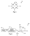
- an exemplary pressure sensor 10 that includes a plurality of resistors R1-R4, which are connected in a Wheatstone bridge configuration.
- the resistance of the resistors R1 and R3 decrease in magnitude proportional to an applied pressure and the resistance of the resistors R2 and R4 increase in magnitude proportional to an applied pressure.
- These resistive changes cause a voltage V 0 + to increase and the voltage V 0 - to decrease at the output of the sensor 10, producing a differential output voltage that is proportional to an applied pressure.
- the pressure sensor 10 is shown coupled to a compensation circuit 100.
- the compensation circuit 100 includes a voltage to current converter and multiplier circuit 102, whose input is coupled to the pressure sensor 10 and whose output is coupled to an inverting input of an operational amplifier 104.
- a current source Is is also coupled to the inverting input of the operational amplifier 104.
- the circuit 102 includes a multiplier that compensates for gain at room temperature and temperature-dependent gain.
- the current source Is compensates for sensor offsets at room temperature and temperature-dependent sensor offsets.
- the current I 0 and Is are converted to an output voltage VOUT, which is provided at an output of the amplifier 104.
- a feedback resistor RFB is coupled between the output of the amplifier 104 and the inverting input of the amplifier 104.
- a load resister RLD is coupled between power supply VDD and the non-inverting input of the amplifier 104.
- a bias voltage (VBIAS) is applied to the non-inverting input of the amplifier 104.
- the resistor RLD provides a current that places the output voltage VOUT of the amplifier 104 at a desired DC voltage offset.
- the output voltage VOUT ranges in value between ground and the supply voltage VDD.
- the output voltage VOUT is proportional to the pressure applied to the sensor.
- a relatively low-cost technique for assembling pressure sensors for motor vehicle applications is described herein.
- the technique allows for integrated pressure sensors to be produced in a high-volume production environment, as it allows for multiple integrated pressure sensors to be calibrated in parallel in a relatively short period of time.
- Fig. 3A depicts a substrate 200 with a plurality of pressure sensors 10 distributed in an array across the face of the substrate 200.
- Fig. 3B depicts a second side of the substrate 200 with a plurality of compensation circuits 100 positioned in an array on the substrate 200.
- the substrate 200 may be, for example, a low-temperature co-fired ceramic (LTCC), or may take other forms, such as a printed circuit board (PCB).
- the compensation circuit 100 may be implemented in an application specific integrated circuit (ASIC) or separate analog circuitry. As previously mentioned, the compensation circuit 100 is located on one side of the substrate 200 and the pressure sensor 10 is located on the opposite side of the substrate 200 to reduce the footprint of the integrated pressure sensor.
- ASIC application specific integrated circuit
- an electromagnetic shield 140 e.g., a metal can, may be implemented for each sensor 10 (to shield the sensor 10 from electromagnetic interference (EMI) and protect the sensor 10 from damage during processing) and an electromagnetic shield 142 may be implemented for each of the compensation circuits 100 (to shield the compensation circuits 100 from EMI and protect the compensation circuits 100 from damage during processing).
- EMI electromagnetic interference
- an electromagnetic shield 142 may be implemented for each of the compensation circuits 100 (to shield the compensation circuits 100 from EMI and protect the compensation circuits 100 from damage during processing).
- Utilizing the manufacturing process described herein allows for a relatively small pressure sensor to be manufactured, e.g., a pressure sensor having a size of 0.3 inch by 0.27 inch. Further, providing the components in an array allows for a number of devices to be processed concurrently. For example, providing compensation circuits and pressure sensors in a 9 by 10 array allows for 90 devices to be concurrently processed. Further, providing the pressure sensors in an array allows for the sensors to be calibrated in parallel. In general, the number of units that can be processed in parallel is determined by the tester capacity, rather than the final assembly size of the pressure sensor. Thus, the manufacturing process can be optimized for a given tester. After calibration, each of the sensor-compensation circuit pairs is singulated for final packaging. The final package can vary in dimension, depending upon a customer's requirements and, thus, the same substrate can be utilized for multiple customers and different packaging requirements.
- Fig. 4 depicts a process 400 for manufacturing an integrated pressure sensor 150, according to the present invention.
- a process 400 is initiated, at which point process step 404 is implemented, where a substrate 200 is positioned to receive a plurality of pressure sensors 10 and compensation circuits 100.
- a plurality of the pressure sensors 10 are positioned on a first side of the substrate 200 in an array.
- a plurality of the compensation circuits 100 are positioned on a second side of the substrate 100 in an array. It should be appreciated that the circuits 100 and the sensors 10 are electrically coupled to conductive electrical traces of the substrate 100 through a conventional process, e.g., a wave solder process.
- step 410 compensation circuit-pressure sensor pairs 150 are calibrated in parallel.
- step 412 the compensation circuit-pressure sensor pairs 150 are singulated to produce individual sensors for final packaging, at which point the process 400 terminates in step 414, where the individual integrated pressure sensors 150 are ready for final packaging.
Landscapes
- Physics & Mathematics (AREA)
- General Physics & Mathematics (AREA)
- Electromagnetism (AREA)
- Measuring Fluid Pressure (AREA)
- Pressure Sensors (AREA)
Abstract
Description
- The present invention is generally directed to a pressure sensor and, more specifically, to an integrated pressure sensor.
- Today, pressure sensors are widely utilized in motor vehicles to control and/or monitor vehicle operation. In general, a pressure sensor provides a relatively accurate analog voltage at its output that is representative of a sensed input pressure. When implemented within a motor vehicle, a pressure sensor may experience temperatures ranging between -40 degrees C to +125 degrees C. In order to provide useful information, the accuracy of an automotive pressure sensor must be maintained over the above-referenced temperature range for the life of an associated motor vehicle.
- Typically, commercially available pressure sensors have been calibrated after incorporation within a final pressure sensor assembly, which has typically included a pressure sensor, a compensation circuit and other associated circuitry. In general, such final pressure sensor assemblies have been relatively large, e.g., at least two inches by one inch. Due to the relatively large size of the assemblies, processing a relatively large number of the assemblies simultaneously has been cost prohibitive.
- What is needed is a technique for producing a relatively low-cost pressure sensor for motor vehicle applications. It would also be desirable for a pressure sensor to be designed so as to be readily producible in a high-volume production environment.
- The present invention is generally directed to a technique for manufacturing an integrated pressure sensor. According to the present invention, a substrate with conductive electrical traces located on first and second sides is provided. A plurality of compensation circuits, which are positioned in an array on the first side of the substrate, are positioned in electrical contact with one or more of the conductive electrical traces on the first side of the substrate. A plurality of pressure sensors are positioned on the second side of the substrate in electrical contact with one or more of the conductive electrical traces on the second side of the substrate. Each one of the sensors is associated with one of the compensation circuits, which is configured to provide temperature compensation for an associated one of the sensors, to form a plurality of pressure sensor-compensation circuit pairs. The substrate also includes conductive vias to electrically connect each of the sensor-compensation circuit pairs. According to the present invention, each of the sensor-compensation circuit pairs is calibrated and singulated for final packaging.
- According to one embodiment of the present invention, the substrate is a low-temperature co-fired ceramic (LTCC). According to another aspect of the present invention, the compensation circuits each include an application specific integrated circuit (ASIC). According to this aspect of the invention, the ASIC is configured to provide temperature and long-term drift compensation of an associated one of the sensors. According to a different aspect of the invention, the array is a 9 by 10 array. According to yet another embodiment of the present invention, the sensor-compensation circuit pairs are calibrated in parallel before singulation.
- These and other features, advantages and objects of the present invention will be further understood and appreciated by those skilled in the art by reference to the following specification, claims and appended drawings.
- The present invention will now be described, by way of example, with reference to the accompanying drawings, in which:
- Fig. 1 is an electrical diagram of a typical pressure sensor;
- Fig. 2 is an electrical diagram in block and schematic form of a pressure sensor coupled to a compensation circuit;
- Fig. 3A-3B are perspective views of a front and rear of an exemplary substrate, including a plurality of pressure sensors and compensation circuits, respectively, constructed according to the present invention; and
- Fig. 4 is a flow chart of a process for manufacturing an integrated pressure sensor, according to the present invention.
- Referring to Fig. 1, an
exemplary pressure sensor 10 is depicted that includes a plurality of resistors R1-R4, which are connected in a Wheatstone bridge configuration. The resistance of the resistors R1 and R3 decrease in magnitude proportional to an applied pressure and the resistance of the resistors R2 and R4 increase in magnitude proportional to an applied pressure. These resistive changes cause a voltage V0+ to increase and the voltage V0- to decrease at the output of thesensor 10, producing a differential output voltage that is proportional to an applied pressure. - With reference to Fig. 2, the
pressure sensor 10 is shown coupled to acompensation circuit 100. Thecompensation circuit 100 includes a voltage to current converter andmultiplier circuit 102, whose input is coupled to thepressure sensor 10 and whose output is coupled to an inverting input of anoperational amplifier 104. As is shown, a current source Is is also coupled to the inverting input of theoperational amplifier 104. Thecircuit 102 includes a multiplier that compensates for gain at room temperature and temperature-dependent gain. - The current source Is compensates for sensor offsets at room temperature and temperature-dependent sensor offsets. The current I0 and Is are converted to an output voltage VOUT, which is provided at an output of the
amplifier 104. As is shown, a feedback resistor RFB is coupled between the output of theamplifier 104 and the inverting input of theamplifier 104. A load resister RLD is coupled between power supply VDD and the non-inverting input of theamplifier 104. A bias voltage (VBIAS) is applied to the non-inverting input of theamplifier 104. The resistor RLD provides a current that places the output voltage VOUT of theamplifier 104 at a desired DC voltage offset. The output voltage VOUT ranges in value between ground and the supply voltage VDD. The output voltage VOUT is proportional to the pressure applied to the sensor. Implementing thecircuit 100 allows for linear errors in gain, offset and temperature dependencies to be compensated. - According to the present invention, a relatively low-cost technique for assembling pressure sensors for motor vehicle applications is described herein. The technique allows for integrated pressure sensors to be produced in a high-volume production environment, as it allows for multiple integrated pressure sensors to be calibrated in parallel in a relatively short period of time.
- Fig. 3A depicts a
substrate 200 with a plurality ofpressure sensors 10 distributed in an array across the face of thesubstrate 200. Fig. 3B depicts a second side of thesubstrate 200 with a plurality ofcompensation circuits 100 positioned in an array on thesubstrate 200. Thesubstrate 200 may be, for example, a low-temperature co-fired ceramic (LTCC), or may take other forms, such as a printed circuit board (PCB). Thecompensation circuit 100 may be implemented in an application specific integrated circuit (ASIC) or separate analog circuitry. As previously mentioned, thecompensation circuit 100 is located on one side of thesubstrate 200 and thepressure sensor 10 is located on the opposite side of thesubstrate 200 to reduce the footprint of the integrated pressure sensor. As is shown for one compensation circuit-pressure sensor pair 150, anelectromagnetic shield 140, e.g., a metal can, may be implemented for each sensor 10 (to shield thesensor 10 from electromagnetic interference (EMI) and protect thesensor 10 from damage during processing) and anelectromagnetic shield 142 may be implemented for each of the compensation circuits 100 (to shield thecompensation circuits 100 from EMI and protect thecompensation circuits 100 from damage during processing). - Utilizing the manufacturing process described herein allows for a relatively small pressure sensor to be manufactured, e.g., a pressure sensor having a size of 0.3 inch by 0.27 inch. Further, providing the components in an array allows for a number of devices to be processed concurrently. For example, providing compensation circuits and pressure sensors in a 9 by 10 array allows for 90 devices to be concurrently processed. Further, providing the pressure sensors in an array allows for the sensors to be calibrated in parallel. In general, the number of units that can be processed in parallel is determined by the tester capacity, rather than the final assembly size of the pressure sensor. Thus, the manufacturing process can be optimized for a given tester. After calibration, each of the sensor-compensation circuit pairs is singulated for final packaging. The final package can vary in dimension, depending upon a customer's requirements and, thus, the same substrate can be utilized for multiple customers and different packaging requirements.
- Fig. 4 depicts a
process 400 for manufacturing anintegrated pressure sensor 150, according to the present invention. Instep 402, aprocess 400 is initiated, at whichpoint process step 404 is implemented, where asubstrate 200 is positioned to receive a plurality ofpressure sensors 10 andcompensation circuits 100. Next, instep 406, a plurality of thepressure sensors 10 are positioned on a first side of thesubstrate 200 in an array. Next, instep 408, a plurality of thecompensation circuits 100 are positioned on a second side of thesubstrate 100 in an array. It should be appreciated that thecircuits 100 and thesensors 10 are electrically coupled to conductive electrical traces of thesubstrate 100 through a conventional process, e.g., a wave solder process. Then, instep 410, compensation circuit-pressure sensor pairs 150 are calibrated in parallel. Next, instep 412, the compensation circuit-pressure sensor pairs 150 are singulated to produce individual sensors for final packaging, at which point theprocess 400 terminates instep 414, where the individualintegrated pressure sensors 150 are ready for final packaging. - Accordingly, a design and manufacturing process have been disclosed herein that allow for micro-package assembly and calibration in plate form. As the final design is relatively small and built in an array, calibration may be performed on multiple units in parallel. Further, the final assembly is independent of the substrate design and calibration process, which allows for a flexible low-cost manufacturing flow. The final product is a low-cost integrated pressure sensor that meets ever-increasing customer requirements.
- The above description is considered that of the preferred embodiments only. Modifications of the invention will occur to those skilled in the art and to those who make or use the invention. Therefore, it is understood that the embodiments shown in the drawings and described above are merely for illustrative purposes and not intended to limit the scope of the invention, which is defined by the following claims as interpreted according to the principles of patent law, including the doctrine of equivalents.
Claims (18)
- A method (400) for manufacturing an integrated pressure sensor, comprising the steps of:providing a substrate with a first side and a second side (404), wherein the substrate includes conductive electrical traces located on the first and second sides;positioning a plurality of compensation circuits on the first side of the substrate in electrical contact with one or more of the conductive electrical traces on the first side of the substrate (408), wherein the compensation circuits are positioned in an array;positioning a plurality of pressure sensors on the second side of the substrate in electrical contact with one or more of the conductive electrical traces on the second side of the substrate (406), wherein each one of the sensors is associated with one of the compensation circuits to form a plurality of pressure sensor-compensation circuit pairs, and wherein the substrate includes conductive vias to electrically connect each of the sensor-compensation circuit pairs, where each of the compensation circuits provides temperature compensation for an associated one of the sensors;calibrating each of the sensor-compensation circuit pairs (410); andsingulating each of the sensor-compensation circuit pairs for final packaging (412).
- The method (400) of claim 1, wherein the substrate is a low-temperature co-fired ceramic (LTCC).
- The method (400) of claim 1, wherein the compensation circuits each include an application specific integrated circuit (ASIC).
- The method (400) of claim 3, wherein the ASIC is configured to provide temperature and long-term drift compensation for an associated one of the sensors.
- The method (400) of claim 1, wherein the array is a 9 by 10 array.
- The method (400) of claim 1, wherein the sensor-compensation circuit pairs are calibrated in parallel.
- A method (400) for manufacturing an integrated pressure sensor, comprising the steps of:providing a substrate with a first side and a second side (404), wherein the substrate includes conductive electrical traces located on the first and second sides;positioning a plurality of compensation circuits on the first side of the substrate in electrical contact with one or more of the conductive electrical traces on the first side of the substrate (408), wherein the compensation circuits are positioned in an array;positioning a plurality of pressure sensors on the second side of the substrate in electrical contact with or more of the conductive electrical traces on the second side of the substrate (406), wherein each one of the sensors is associated with one of the compensation circuits to form a plurality of pressure sensor-compensation circuit pairs, and wherein the substrate includes conductive vias to electrically connect each of the sensor-compensation circuit pairs, where each of the compensation circuits provides temperature compensation for an associated one of the sensors;calibrating each of the sensor-compensation circuit pairs (410), wherein the sensor-compensation circuit pairs are calibrated in parallel; andsingulating each of the sensor-compensation circuit pairs for final packaging (412).
- The method (400) of claim 7, wherein the substrate is a low-temperature co-fired ceramic (LTCC).
- The method (400) of claim 7, wherein the substrate is a printed circuit board (PCB).
- The method (400) of claim 7, wherein the compensation circuits each include an application specific integrated circuit (ASIC).
- The method (400) of claim 10, wherein the ASIC is configured to provide temperature and long-term drift compensation for an associated one of the sensors.
- The method (400) of claim 7, wherein the array is a 9 by 10 array.
- An integrated pressure sensor assembly (150), comprising:a substrate (200) with a first side and a second side, wherein the substrate (200) includes conductive electrical traces located on the first and second sides;a plurality of compensation circuits (100) positioned on the first side of the substrate (200) in electrical contact with one or more of the conductive electrical traces on the first side of the substrate (200), wherein the compensation circuits (100) are positioned in an array; anda plurality of pressure sensors (10) positioned on the second side of the substrate (200) in electrical contact with one or more of the conductive electrical traces on the second side of the substrate (200), wherein each one of the sensors (10) is associated with one of the compensation circuits (100) to form a plurality of pressure sensor-compensation circuit pairs, and wherein the substrate (200) includes conductive vias to electrically connect the sensor-compensation circuit pairs, where each of the compensation circuits (100) provides temperature compensation for an associated one of the sensors, and where each of the sensor-compensation circuit pairs are calibrated in parallel before being singulated for final packaging.
- The integrated pressure sensor assembly (150) of claim 13, wherein the substrate (200) is a low-temperature co-fired ceramic (LTCC).
- The integrated pressure sensor assembly (150) of claim 13, wherein the substrate (200) is a printed circuit board (PCB).
- The integrated pressure sensor assembly (150) of claim 13, wherein the compensation circuits (100) each include an application specific integrated circuit (ASIC).
- The integrated pressure sensor assembly (150) of claim 16, wherein the ASIC is configured to provide temperature and long-term drift compensation for an associated one of the sensors (10).
- The integrated pressure sensor assembly (150) of claim 13, wherein the array is a 9 by 10 array.
Applications Claiming Priority (1)
| Application Number | Priority Date | Filing Date | Title |
|---|---|---|---|
| US11/028,343 US7117747B2 (en) | 2005-01-03 | 2005-01-03 | Integrated pressure sensor and method of manufacture |
Publications (2)
| Publication Number | Publication Date |
|---|---|
| EP1677089A1 true EP1677089A1 (en) | 2006-07-05 |
| EP1677089B1 EP1677089B1 (en) | 2008-03-26 |
Family
ID=36192883
Family Applications (1)
| Application Number | Title | Priority Date | Filing Date |
|---|---|---|---|
| EP05077861A Expired - Lifetime EP1677089B1 (en) | 2005-01-03 | 2005-12-12 | Integrated pressure sensor and method of manufacture |
Country Status (4)
| Country | Link |
|---|---|
| US (1) | US7117747B2 (en) |
| EP (1) | EP1677089B1 (en) |
| AT (1) | ATE390623T1 (en) |
| DE (1) | DE602005005616T2 (en) |
Families Citing this family (11)
| Publication number | Priority date | Publication date | Assignee | Title |
|---|---|---|---|---|
| US7174773B2 (en) * | 2005-04-19 | 2007-02-13 | Delphi Technologies, Inc. | Leak-testing technique for differential pressure sensor array |
| US7950286B2 (en) * | 2008-12-19 | 2011-05-31 | Honeywell International Inc. | Multi-range pressure sensor apparatus and method utilizing a single sense die and multiple signal paths |
| US10330513B2 (en) * | 2009-05-27 | 2019-06-25 | Honeywell International Inc. | Multi-dynamic-range sensor |
| US8656772B2 (en) | 2010-03-22 | 2014-02-25 | Honeywell International Inc. | Flow sensor with pressure output signal |
| US8695417B2 (en) | 2011-01-31 | 2014-04-15 | Honeywell International Inc. | Flow sensor with enhanced flow range capability |
| US8446220B2 (en) | 2011-05-09 | 2013-05-21 | Honeywell International Inc. | Method and apparatus for increasing the effective resolution of a sensor |
| US8770034B2 (en) | 2011-09-06 | 2014-07-08 | Honeywell International Inc. | Packaged sensor with multiple sensors elements |
| US9052217B2 (en) | 2012-11-09 | 2015-06-09 | Honeywell International Inc. | Variable scale sensor |
| US11378468B2 (en) * | 2016-08-12 | 2022-07-05 | Brightsentinel Limited | Sensor module and process for producing same |
| DE102023110113A1 (en) * | 2023-04-20 | 2024-10-24 | Tdk Electronics Ag | Sensor arrangement and method for producing a plurality of sensor arrangements |
| CN121163755A (en) * | 2025-10-09 | 2025-12-19 | 歌尔微电子股份有限公司 | Pressure sensor, calibration method of pressure sensor and electronic equipment |
Citations (12)
| Publication number | Priority date | Publication date | Assignee | Title |
|---|---|---|---|---|
| US3886799A (en) * | 1973-09-24 | 1975-06-03 | Nat Semiconductor Corp | Semiconductor pressure transducer employing temperature compensation circuits and novel heater circuitry |
| US4390028A (en) * | 1980-03-24 | 1983-06-28 | Kabushiki Kaisha Morita Seisakusho | Occlusion pressure sensor |
| US4404539A (en) * | 1980-02-22 | 1983-09-13 | Hitachi, Ltd. | Semiconductor strain gauge |
| US4556807A (en) * | 1982-08-16 | 1985-12-03 | Hitachi, Ltd. | Pressure transducer with temperature compensation circuit |
| JPH01199476A (en) * | 1987-10-28 | 1989-08-10 | Komatsu Ltd | Pressure sensor |
| US4986131A (en) * | 1988-12-28 | 1991-01-22 | Kabushiki Kaisha Toyota Chuo Kenkyusho | Semiconductor strain detector |
| US5431057A (en) * | 1990-02-12 | 1995-07-11 | Fraunhofer-Gesellschaft Zur Forderung Der Angewandten Forschung E.V. | Integratable capacitative pressure sensor |
| EP0677725A1 (en) * | 1994-04-15 | 1995-10-18 | Ssi Technologies, Inc. | Improved electronic circuit for a transducer |
| US5581038A (en) * | 1994-04-04 | 1996-12-03 | Sentir, Inc. | Pressure measurement apparatus having a reverse mounted transducer and overpressure guard |
| EP0964252A1 (en) * | 1998-06-09 | 1999-12-15 | Fraunhofer-Gesellschaft Zur Förderung Der Angewandten Forschung E.V. | Device for measuring the extension and/or compression of an object |
| EP1300664A1 (en) * | 2000-07-13 | 2003-04-09 | Mitsubishi Denki Kabushiki Kaisha | Pressure sensor |
| US20040079159A1 (en) * | 2002-07-13 | 2004-04-29 | Joerg Muchow | Micromechanical pressure sensor device and corresponding measurement system |
Family Cites Families (14)
| Publication number | Priority date | Publication date | Assignee | Title |
|---|---|---|---|---|
| US5062302A (en) * | 1988-04-29 | 1991-11-05 | Schlumberger Industries, Inc. | Laminated semiconductor sensor with overpressure protection |
| JP3203788B2 (en) * | 1992-07-24 | 2001-08-27 | オムロン株式会社 | Physical quantity sensor and method of manufacturing the same |
| EP0702221A3 (en) * | 1994-09-14 | 1997-05-21 | Delco Electronics Corp | Built-in single chip sensor |
| US5700981A (en) * | 1996-02-08 | 1997-12-23 | Micron Communications, Inc. | Encapsulated electronic component and method for encapsulating an electronic component |
| US5981314A (en) * | 1996-10-31 | 1999-11-09 | Amkor Technology, Inc. | Near chip size integrated circuit package |
| JP3299715B2 (en) * | 1998-04-01 | 2002-07-08 | 長野計器株式会社 | Chip potential extraction structure and manufacturing method |
| US6229404B1 (en) * | 1998-08-31 | 2001-05-08 | Kyocera Corporation | Crystal oscillator |
| DE10022124B4 (en) * | 2000-05-06 | 2010-01-14 | Wabco Gmbh | Electronic control unit |
| WO2002096166A1 (en) * | 2001-05-18 | 2002-11-28 | Corporation For National Research Initiatives | Radio frequency microelectromechanical systems (mems) devices on low-temperature co-fired ceramic (ltcc) substrates |
| JP3891037B2 (en) * | 2002-05-21 | 2007-03-07 | 株式会社デンソー | Semiconductor pressure sensor and semiconductor wafer for semiconductor pressure sensor |
| US6710461B2 (en) * | 2002-06-06 | 2004-03-23 | Lightuning Tech. Inc. | Wafer level packaging of micro electromechanical device |
| US6833645B2 (en) * | 2002-11-18 | 2004-12-21 | Harris Corporation | Micro-electromechanical voltage converter |
| JP2004177343A (en) * | 2002-11-28 | 2004-06-24 | Fujikura Ltd | Pressure sensor |
| JP2005180930A (en) * | 2003-12-16 | 2005-07-07 | Ricoh Co Ltd | Semiconductor sensor device and manufacturing method thereof |
-
2005
- 2005-01-03 US US11/028,343 patent/US7117747B2/en not_active Expired - Lifetime
- 2005-12-12 AT AT05077861T patent/ATE390623T1/en not_active IP Right Cessation
- 2005-12-12 DE DE602005005616T patent/DE602005005616T2/en not_active Expired - Lifetime
- 2005-12-12 EP EP05077861A patent/EP1677089B1/en not_active Expired - Lifetime
Patent Citations (12)
| Publication number | Priority date | Publication date | Assignee | Title |
|---|---|---|---|---|
| US3886799A (en) * | 1973-09-24 | 1975-06-03 | Nat Semiconductor Corp | Semiconductor pressure transducer employing temperature compensation circuits and novel heater circuitry |
| US4404539A (en) * | 1980-02-22 | 1983-09-13 | Hitachi, Ltd. | Semiconductor strain gauge |
| US4390028A (en) * | 1980-03-24 | 1983-06-28 | Kabushiki Kaisha Morita Seisakusho | Occlusion pressure sensor |
| US4556807A (en) * | 1982-08-16 | 1985-12-03 | Hitachi, Ltd. | Pressure transducer with temperature compensation circuit |
| JPH01199476A (en) * | 1987-10-28 | 1989-08-10 | Komatsu Ltd | Pressure sensor |
| US4986131A (en) * | 1988-12-28 | 1991-01-22 | Kabushiki Kaisha Toyota Chuo Kenkyusho | Semiconductor strain detector |
| US5431057A (en) * | 1990-02-12 | 1995-07-11 | Fraunhofer-Gesellschaft Zur Forderung Der Angewandten Forschung E.V. | Integratable capacitative pressure sensor |
| US5581038A (en) * | 1994-04-04 | 1996-12-03 | Sentir, Inc. | Pressure measurement apparatus having a reverse mounted transducer and overpressure guard |
| EP0677725A1 (en) * | 1994-04-15 | 1995-10-18 | Ssi Technologies, Inc. | Improved electronic circuit for a transducer |
| EP0964252A1 (en) * | 1998-06-09 | 1999-12-15 | Fraunhofer-Gesellschaft Zur Förderung Der Angewandten Forschung E.V. | Device for measuring the extension and/or compression of an object |
| EP1300664A1 (en) * | 2000-07-13 | 2003-04-09 | Mitsubishi Denki Kabushiki Kaisha | Pressure sensor |
| US20040079159A1 (en) * | 2002-07-13 | 2004-04-29 | Joerg Muchow | Micromechanical pressure sensor device and corresponding measurement system |
Non-Patent Citations (1)
| Title |
|---|
| PATENT ABSTRACTS OF JAPAN vol. 013, no. 496 (E - 843) 9 November 1989 (1989-11-09) * |
Also Published As
| Publication number | Publication date |
|---|---|
| DE602005005616D1 (en) | 2008-05-08 |
| DE602005005616T2 (en) | 2009-05-07 |
| US20060144156A1 (en) | 2006-07-06 |
| EP1677089B1 (en) | 2008-03-26 |
| ATE390623T1 (en) | 2008-04-15 |
| US7117747B2 (en) | 2006-10-10 |
Similar Documents
| Publication | Publication Date | Title |
|---|---|---|
| US10989741B2 (en) | Current sensor | |
| US8490496B2 (en) | Multi range pressure sensor apparatus and method utilizing a single sense die and multiple signal paths | |
| CA2145698C (en) | Electronic circuit for a transducer | |
| JP3399953B2 (en) | Pressure sensor | |
| US7117747B2 (en) | Integrated pressure sensor and method of manufacture | |
| US11415472B2 (en) | Flexible bridge sensor electronic architecture and method for implementing same | |
| JPH10281897A (en) | Semiconductor pressure detector | |
| US20140137651A1 (en) | System and method for passively compensating pressure sensors | |
| CN109443503B (en) | Detection device | |
| US7146862B2 (en) | Thick film strain gage sensor | |
| EP0441549B1 (en) | Matched pair of sensor and amplifier circuits | |
| US6490926B2 (en) | Acceleration sensor module | |
| JP3373603B2 (en) | Bridge circuit for sensor | |
| JPH07212139A (en) | Sensor detection circuit | |
| US6993975B2 (en) | Pressure sensor module having stress isolation platform | |
| JPH0534182A (en) | Strain / temperature combined sensor | |
| JP2934538B2 (en) | Transducer circuit and manufacturing method thereof | |
| JP2002372474A (en) | Semiconductor sensor device | |
| US20060087326A1 (en) | Resistive sensing element circuit | |
| KR100238776B1 (en) | Temperature compensation method for pressure sensor and apparatus using the same | |
| US20240328874A1 (en) | Stress-compensated wheatstone heater and thermometer in resistive microelectromechanical system pressure sensors | |
| Pelicia et al. | Fully integrated programmable Howland current source for sensors excitation | |
| WO2024199882A1 (en) | Integrated circuit chip with stress compensation circuit | |
| JP2003207406A (en) | Semiconductor sensor device | |
| JPH0368830A (en) | Temperature compensation circuit of semiconductor pressure sensor |
Legal Events
| Date | Code | Title | Description |
|---|---|---|---|
| PUAI | Public reference made under article 153(3) epc to a published international application that has entered the european phase |
Free format text: ORIGINAL CODE: 0009012 |
|
| AK | Designated contracting states |
Kind code of ref document: A1 Designated state(s): AT BE BG CH CY CZ DE DK EE ES FI FR GB GR HU IE IS IT LI LT LU LV MC NL PL PT RO SE SI SK TR |
|
| AX | Request for extension of the european patent |
Extension state: AL BA HR MK YU |
|
| 17P | Request for examination filed |
Effective date: 20070105 |
|
| AKX | Designation fees paid |
Designated state(s): AT BE BG CH CY CZ DE DK EE ES FI FR GB GR HU IE IS IT LI LT LU LV MC NL PL PT RO SE SI SK TR |
|
| GRAP | Despatch of communication of intention to grant a patent |
Free format text: ORIGINAL CODE: EPIDOSNIGR1 |
|
| GRAS | Grant fee paid |
Free format text: ORIGINAL CODE: EPIDOSNIGR3 |
|
| GRAA | (expected) grant |
Free format text: ORIGINAL CODE: 0009210 |
|
| AK | Designated contracting states |
Kind code of ref document: B1 Designated state(s): AT BE BG CH CY CZ DE DK EE ES FI FR GB GR HU IE IS IT LI LT LU LV MC NL PL PT RO SE SI SK TR |
|
| REG | Reference to a national code |
Ref country code: GB Ref legal event code: FG4D |
|
| REG | Reference to a national code |
Ref country code: CH Ref legal event code: EP Ref country code: IE Ref legal event code: FG4D |
|
| REF | Corresponds to: |
Ref document number: 602005005616 Country of ref document: DE Date of ref document: 20080508 Kind code of ref document: P |
|
| PG25 | Lapsed in a contracting state [announced via postgrant information from national office to epo] |
Ref country code: FI Free format text: LAPSE BECAUSE OF FAILURE TO SUBMIT A TRANSLATION OF THE DESCRIPTION OR TO PAY THE FEE WITHIN THE PRESCRIBED TIME-LIMIT Effective date: 20080326 |
|
| PG25 | Lapsed in a contracting state [announced via postgrant information from national office to epo] |
Ref country code: AT Free format text: LAPSE BECAUSE OF FAILURE TO SUBMIT A TRANSLATION OF THE DESCRIPTION OR TO PAY THE FEE WITHIN THE PRESCRIBED TIME-LIMIT Effective date: 20080326 |
|
| NLV1 | Nl: lapsed or annulled due to failure to fulfill the requirements of art. 29p and 29m of the patents act | ||
| PG25 | Lapsed in a contracting state [announced via postgrant information from national office to epo] |
Ref country code: BE Free format text: LAPSE BECAUSE OF FAILURE TO SUBMIT A TRANSLATION OF THE DESCRIPTION OR TO PAY THE FEE WITHIN THE PRESCRIBED TIME-LIMIT Effective date: 20080326 Ref country code: LV Free format text: LAPSE BECAUSE OF FAILURE TO SUBMIT A TRANSLATION OF THE DESCRIPTION OR TO PAY THE FEE WITHIN THE PRESCRIBED TIME-LIMIT Effective date: 20080326 Ref country code: PL Free format text: LAPSE BECAUSE OF FAILURE TO SUBMIT A TRANSLATION OF THE DESCRIPTION OR TO PAY THE FEE WITHIN THE PRESCRIBED TIME-LIMIT Effective date: 20080326 Ref country code: SI Free format text: LAPSE BECAUSE OF FAILURE TO SUBMIT A TRANSLATION OF THE DESCRIPTION OR TO PAY THE FEE WITHIN THE PRESCRIBED TIME-LIMIT Effective date: 20080326 |
|
| PG25 | Lapsed in a contracting state [announced via postgrant information from national office to epo] |
Ref country code: SK Free format text: LAPSE BECAUSE OF FAILURE TO SUBMIT A TRANSLATION OF THE DESCRIPTION OR TO PAY THE FEE WITHIN THE PRESCRIBED TIME-LIMIT Effective date: 20080326 Ref country code: SE Free format text: LAPSE BECAUSE OF FAILURE TO SUBMIT A TRANSLATION OF THE DESCRIPTION OR TO PAY THE FEE WITHIN THE PRESCRIBED TIME-LIMIT Effective date: 20080626 Ref country code: ES Free format text: LAPSE BECAUSE OF FAILURE TO SUBMIT A TRANSLATION OF THE DESCRIPTION OR TO PAY THE FEE WITHIN THE PRESCRIBED TIME-LIMIT Effective date: 20080707 Ref country code: PT Free format text: LAPSE BECAUSE OF FAILURE TO SUBMIT A TRANSLATION OF THE DESCRIPTION OR TO PAY THE FEE WITHIN THE PRESCRIBED TIME-LIMIT Effective date: 20080901 Ref country code: CZ Free format text: LAPSE BECAUSE OF FAILURE TO SUBMIT A TRANSLATION OF THE DESCRIPTION OR TO PAY THE FEE WITHIN THE PRESCRIBED TIME-LIMIT Effective date: 20080326 |
|
| PG25 | Lapsed in a contracting state [announced via postgrant information from national office to epo] |
Ref country code: RO Free format text: LAPSE BECAUSE OF FAILURE TO SUBMIT A TRANSLATION OF THE DESCRIPTION OR TO PAY THE FEE WITHIN THE PRESCRIBED TIME-LIMIT Effective date: 20080326 Ref country code: NL Free format text: LAPSE BECAUSE OF FAILURE TO SUBMIT A TRANSLATION OF THE DESCRIPTION OR TO PAY THE FEE WITHIN THE PRESCRIBED TIME-LIMIT Effective date: 20080326 |
|
| PG25 | Lapsed in a contracting state [announced via postgrant information from national office to epo] |
Ref country code: IS Free format text: LAPSE BECAUSE OF FAILURE TO SUBMIT A TRANSLATION OF THE DESCRIPTION OR TO PAY THE FEE WITHIN THE PRESCRIBED TIME-LIMIT Effective date: 20080726 |
|
| EN | Fr: translation not filed | ||
| PG25 | Lapsed in a contracting state [announced via postgrant information from national office to epo] |
Ref country code: DK Free format text: LAPSE BECAUSE OF FAILURE TO SUBMIT A TRANSLATION OF THE DESCRIPTION OR TO PAY THE FEE WITHIN THE PRESCRIBED TIME-LIMIT Effective date: 20080326 Ref country code: LT Free format text: LAPSE BECAUSE OF FAILURE TO SUBMIT A TRANSLATION OF THE DESCRIPTION OR TO PAY THE FEE WITHIN THE PRESCRIBED TIME-LIMIT Effective date: 20080326 |
|
| PLBE | No opposition filed within time limit |
Free format text: ORIGINAL CODE: 0009261 |
|
| STAA | Information on the status of an ep patent application or granted ep patent |
Free format text: STATUS: NO OPPOSITION FILED WITHIN TIME LIMIT |
|
| 26N | No opposition filed |
Effective date: 20081230 |
|
| PG25 | Lapsed in a contracting state [announced via postgrant information from national office to epo] |
Ref country code: BG Free format text: LAPSE BECAUSE OF FAILURE TO SUBMIT A TRANSLATION OF THE DESCRIPTION OR TO PAY THE FEE WITHIN THE PRESCRIBED TIME-LIMIT Effective date: 20080626 Ref country code: FR Free format text: LAPSE BECAUSE OF FAILURE TO SUBMIT A TRANSLATION OF THE DESCRIPTION OR TO PAY THE FEE WITHIN THE PRESCRIBED TIME-LIMIT Effective date: 20090116 Ref country code: EE Free format text: LAPSE BECAUSE OF FAILURE TO SUBMIT A TRANSLATION OF THE DESCRIPTION OR TO PAY THE FEE WITHIN THE PRESCRIBED TIME-LIMIT Effective date: 20080326 |
|
| PG25 | Lapsed in a contracting state [announced via postgrant information from national office to epo] |
Ref country code: MC Free format text: LAPSE BECAUSE OF NON-PAYMENT OF DUE FEES Effective date: 20081231 |
|
| PG25 | Lapsed in a contracting state [announced via postgrant information from national office to epo] |
Ref country code: CY Free format text: LAPSE BECAUSE OF FAILURE TO SUBMIT A TRANSLATION OF THE DESCRIPTION OR TO PAY THE FEE WITHIN THE PRESCRIBED TIME-LIMIT Effective date: 20080326 |
|
| PG25 | Lapsed in a contracting state [announced via postgrant information from national office to epo] |
Ref country code: IE Free format text: LAPSE BECAUSE OF NON-PAYMENT OF DUE FEES Effective date: 20081212 |
|
| PG25 | Lapsed in a contracting state [announced via postgrant information from national office to epo] |
Ref country code: HU Free format text: LAPSE BECAUSE OF FAILURE TO SUBMIT A TRANSLATION OF THE DESCRIPTION OR TO PAY THE FEE WITHIN THE PRESCRIBED TIME-LIMIT Effective date: 20080927 Ref country code: LU Free format text: LAPSE BECAUSE OF NON-PAYMENT OF DUE FEES Effective date: 20081212 |
|
| REG | Reference to a national code |
Ref country code: CH Ref legal event code: PL |
|
| GBPC | Gb: european patent ceased through non-payment of renewal fee |
Effective date: 20091212 |
|
| PG25 | Lapsed in a contracting state [announced via postgrant information from national office to epo] |
Ref country code: TR Free format text: LAPSE BECAUSE OF FAILURE TO SUBMIT A TRANSLATION OF THE DESCRIPTION OR TO PAY THE FEE WITHIN THE PRESCRIBED TIME-LIMIT Effective date: 20080326 |
|
| PG25 | Lapsed in a contracting state [announced via postgrant information from national office to epo] |
Ref country code: LI Free format text: LAPSE BECAUSE OF NON-PAYMENT OF DUE FEES Effective date: 20091231 Ref country code: GR Free format text: LAPSE BECAUSE OF FAILURE TO SUBMIT A TRANSLATION OF THE DESCRIPTION OR TO PAY THE FEE WITHIN THE PRESCRIBED TIME-LIMIT Effective date: 20080627 Ref country code: CH Free format text: LAPSE BECAUSE OF NON-PAYMENT OF DUE FEES Effective date: 20091231 |
|
| PG25 | Lapsed in a contracting state [announced via postgrant information from national office to epo] |
Ref country code: GB Free format text: LAPSE BECAUSE OF NON-PAYMENT OF DUE FEES Effective date: 20091212 |
|
| PG25 | Lapsed in a contracting state [announced via postgrant information from national office to epo] |
Ref country code: IT Free format text: LAPSE BECAUSE OF NON-PAYMENT OF DUE FEES Effective date: 20151212 |
|
| PG25 | Lapsed in a contracting state [announced via postgrant information from national office to epo] |
Ref country code: IT Free format text: LAPSE BECAUSE OF NON-PAYMENT OF DUE FEES Effective date: 20151212 |
|
| PGRI | Patent reinstated in contracting state [announced from national office to epo] |
Ref country code: IT Effective date: 20170710 |
|
| REG | Reference to a national code |
Ref country code: DE Ref legal event code: R082 Ref document number: 602005005616 Country of ref document: DE Representative=s name: MANITZ FINSTERWALD PATENT- UND RECHTSANWALTSPA, DE Ref country code: DE Ref legal event code: R081 Ref document number: 602005005616 Country of ref document: DE Owner name: DELPHI TECHNOLOGIES IP LIMITED, BB Free format text: FORMER OWNER: DELPHI TECHNOLOGIES, INC., TROY, MICH., US |
|
| P01 | Opt-out of the competence of the unified patent court (upc) registered |
Effective date: 20230327 |
|
| PGFP | Annual fee paid to national office [announced via postgrant information from national office to epo] |
Ref country code: DE Payment date: 20241111 Year of fee payment: 20 |
|
| PGFP | Annual fee paid to national office [announced via postgrant information from national office to epo] |
Ref country code: IT Payment date: 20241217 Year of fee payment: 20 |
|
| REG | Reference to a national code |
Ref country code: DE Ref legal event code: R071 Ref document number: 602005005616 Country of ref document: DE |