EP1674873A2 - Sensor - Google Patents
Sensor Download PDFInfo
- Publication number
- EP1674873A2 EP1674873A2 EP20060005170 EP06005170A EP1674873A2 EP 1674873 A2 EP1674873 A2 EP 1674873A2 EP 20060005170 EP20060005170 EP 20060005170 EP 06005170 A EP06005170 A EP 06005170A EP 1674873 A2 EP1674873 A2 EP 1674873A2
- Authority
- EP
- European Patent Office
- Prior art keywords
- sensor
- controller
- operating mode
- loop filter
- clock
- Prior art date
- Legal status (The legal status is an assumption and is not a legal conclusion. Google has not performed a legal analysis and makes no representation as to the accuracy of the status listed.)
- Granted
Links
Images


Classifications
-
- G—PHYSICS
- G01—MEASURING; TESTING
- G01P—MEASURING LINEAR OR ANGULAR SPEED, ACCELERATION, DECELERATION, OR SHOCK; INDICATING PRESENCE, ABSENCE, OR DIRECTION, OF MOVEMENT
- G01P1/00—Details of instruments
- G01P1/02—Housings
- G01P1/023—Housings for acceleration measuring devices
-
- B—PERFORMING OPERATIONS; TRANSPORTING
- B81—MICROSTRUCTURAL TECHNOLOGY
- B81B—MICROSTRUCTURAL DEVICES OR SYSTEMS, e.g. MICROMECHANICAL DEVICES
- B81B3/00—Devices comprising flexible or deformable elements, e.g. comprising elastic tongues or membranes
- B81B3/0002—Arrangements for avoiding sticking of the flexible or moving parts
- B81B3/001—Structures having a reduced contact area, e.g. with bumps or with a textured surface
-
- B—PERFORMING OPERATIONS; TRANSPORTING
- B81—MICROSTRUCTURAL TECHNOLOGY
- B81B—MICROSTRUCTURAL DEVICES OR SYSTEMS, e.g. MICROMECHANICAL DEVICES
- B81B3/00—Devices comprising flexible or deformable elements, e.g. comprising elastic tongues or membranes
- B81B3/0064—Constitution or structural means for improving or controlling the physical properties of a device
- B81B3/0067—Mechanical properties
- B81B3/0072—For controlling internal stress or strain in moving or flexible elements, e.g. stress compensating layers
-
- B—PERFORMING OPERATIONS; TRANSPORTING
- B81—MICROSTRUCTURAL TECHNOLOGY
- B81B—MICROSTRUCTURAL DEVICES OR SYSTEMS, e.g. MICROMECHANICAL DEVICES
- B81B7/00—Microstructural systems; Auxiliary parts of microstructural devices or systems
- B81B7/0009—Structural features, others than packages, for protecting a device against environmental influences
- B81B7/0016—Protection against shocks or vibrations, e.g. vibration damping
-
- G—PHYSICS
- G01—MEASURING; TESTING
- G01D—MEASURING NOT SPECIALLY ADAPTED FOR A SPECIFIC VARIABLE; ARRANGEMENTS FOR MEASURING TWO OR MORE VARIABLES NOT COVERED IN A SINGLE OTHER SUBCLASS; TARIFF METERING APPARATUS; MEASURING OR TESTING NOT OTHERWISE PROVIDED FOR
- G01D11/00—Component parts of measuring arrangements not specially adapted for a specific variable
- G01D11/24—Housings ; Casings for instruments
- G01D11/245—Housings for sensors
-
- G—PHYSICS
- G01—MEASURING; TESTING
- G01D—MEASURING NOT SPECIALLY ADAPTED FOR A SPECIFIC VARIABLE; ARRANGEMENTS FOR MEASURING TWO OR MORE VARIABLES NOT COVERED IN A SINGLE OTHER SUBCLASS; TARIFF METERING APPARATUS; MEASURING OR TESTING NOT OTHERWISE PROVIDED FOR
- G01D18/00—Testing or calibrating apparatus or arrangements provided for in groups G01D1/00 - G01D15/00
- G01D18/008—Testing or calibrating apparatus or arrangements provided for in groups G01D1/00 - G01D15/00 with calibration coefficients stored in memory
-
- G—PHYSICS
- G01—MEASURING; TESTING
- G01P—MEASURING LINEAR OR ANGULAR SPEED, ACCELERATION, DECELERATION, OR SHOCK; INDICATING PRESENCE, ABSENCE, OR DIRECTION, OF MOVEMENT
- G01P15/00—Measuring acceleration; Measuring deceleration; Measuring shock, i.e. sudden change of acceleration
- G01P15/02—Measuring acceleration; Measuring deceleration; Measuring shock, i.e. sudden change of acceleration by making use of inertia forces using solid seismic masses
- G01P15/08—Measuring acceleration; Measuring deceleration; Measuring shock, i.e. sudden change of acceleration by making use of inertia forces using solid seismic masses with conversion into electric or magnetic values
- G01P15/0802—Details
-
- G—PHYSICS
- G01—MEASURING; TESTING
- G01P—MEASURING LINEAR OR ANGULAR SPEED, ACCELERATION, DECELERATION, OR SHOCK; INDICATING PRESENCE, ABSENCE, OR DIRECTION, OF MOVEMENT
- G01P15/00—Measuring acceleration; Measuring deceleration; Measuring shock, i.e. sudden change of acceleration
- G01P15/02—Measuring acceleration; Measuring deceleration; Measuring shock, i.e. sudden change of acceleration by making use of inertia forces using solid seismic masses
- G01P15/08—Measuring acceleration; Measuring deceleration; Measuring shock, i.e. sudden change of acceleration by making use of inertia forces using solid seismic masses with conversion into electric or magnetic values
- G01P15/13—Measuring acceleration; Measuring deceleration; Measuring shock, i.e. sudden change of acceleration by making use of inertia forces using solid seismic masses with conversion into electric or magnetic values by measuring the force required to restore a proofmass subjected to inertial forces to a null position
-
- G—PHYSICS
- G01—MEASURING; TESTING
- G01P—MEASURING LINEAR OR ANGULAR SPEED, ACCELERATION, DECELERATION, OR SHOCK; INDICATING PRESENCE, ABSENCE, OR DIRECTION, OF MOVEMENT
- G01P21/00—Testing or calibrating of apparatus or devices covered by the preceding groups
-
- G—PHYSICS
- G01—MEASURING; TESTING
- G01V—GEOPHYSICS; GRAVITATIONAL MEASUREMENTS; DETECTING MASSES OR OBJECTS; TAGS
- G01V1/00—Seismology; Seismic or acoustic prospecting or detecting
- G01V1/02—Generating seismic energy
- G01V1/04—Details
- G01V1/047—Arrangements for coupling the generator to the ground
- G01V1/053—Arrangements for coupling the generator to the ground for generating transverse waves
-
- G—PHYSICS
- G01—MEASURING; TESTING
- G01V—GEOPHYSICS; GRAVITATIONAL MEASUREMENTS; DETECTING MASSES OR OBJECTS; TAGS
- G01V1/00—Seismology; Seismic or acoustic prospecting or detecting
- G01V1/02—Generating seismic energy
- G01V1/104—Generating seismic energy using explosive charges
-
- G—PHYSICS
- G01—MEASURING; TESTING
- G01V—GEOPHYSICS; GRAVITATIONAL MEASUREMENTS; DETECTING MASSES OR OBJECTS; TAGS
- G01V1/00—Seismology; Seismic or acoustic prospecting or detecting
- G01V1/16—Receiving elements for seismic signals; Arrangements or adaptations of receiving elements
- G01V1/18—Receiving elements, e.g. seismometer, geophone or torque detectors, for localised single point measurements
- G01V1/181—Geophones
-
- G—PHYSICS
- G01—MEASURING; TESTING
- G01V—GEOPHYSICS; GRAVITATIONAL MEASUREMENTS; DETECTING MASSES OR OBJECTS; TAGS
- G01V1/00—Seismology; Seismic or acoustic prospecting or detecting
- G01V1/16—Receiving elements for seismic signals; Arrangements or adaptations of receiving elements
- G01V1/18—Receiving elements, e.g. seismometer, geophone or torque detectors, for localised single point measurements
- G01V1/186—Hydrophones
-
- B—PERFORMING OPERATIONS; TRANSPORTING
- B81—MICROSTRUCTURAL TECHNOLOGY
- B81B—MICROSTRUCTURAL DEVICES OR SYSTEMS, e.g. MICROMECHANICAL DEVICES
- B81B2201/00—Specific applications of microelectromechanical systems
- B81B2201/02—Sensors
- B81B2201/0228—Inertial sensors
- B81B2201/0235—Accelerometers
-
- G—PHYSICS
- G01—MEASURING; TESTING
- G01N—INVESTIGATING OR ANALYSING MATERIALS BY DETERMINING THEIR CHEMICAL OR PHYSICAL PROPERTIES
- G01N1/00—Sampling; Preparing specimens for investigation
- G01N1/02—Devices for withdrawing samples
- G01N2001/021—Correlating sampling sites with geographical information, e.g. GPS
-
- H—ELECTRICITY
- H01—ELECTRIC ELEMENTS
- H01L—SEMICONDUCTOR DEVICES NOT COVERED BY CLASS H10
- H01L2224/00—Indexing scheme for arrangements for connecting or disconnecting semiconductor or solid-state bodies and methods related thereto as covered by H01L24/00
- H01L2224/01—Means for bonding being attached to, or being formed on, the surface to be connected, e.g. chip-to-package, die-attach, "first-level" interconnects; Manufacturing methods related thereto
- H01L2224/42—Wire connectors; Manufacturing methods related thereto
- H01L2224/47—Structure, shape, material or disposition of the wire connectors after the connecting process
- H01L2224/48—Structure, shape, material or disposition of the wire connectors after the connecting process of an individual wire connector
- H01L2224/484—Connecting portions
- H01L2224/4847—Connecting portions the connecting portion on the bonding area of the semiconductor or solid-state body being a wedge bond
- H01L2224/48472—Connecting portions the connecting portion on the bonding area of the semiconductor or solid-state body being a wedge bond the other connecting portion not on the bonding area also being a wedge bond, i.e. wedge-to-wedge
-
- H—ELECTRICITY
- H01—ELECTRIC ELEMENTS
- H01L—SEMICONDUCTOR DEVICES NOT COVERED BY CLASS H10
- H01L2924/00—Indexing scheme for arrangements or methods for connecting or disconnecting semiconductor or solid-state bodies as covered by H01L24/00
- H01L2924/0001—Technical content checked by a classifier
- H01L2924/0002—Not covered by any one of groups H01L24/00, H01L24/00 and H01L2224/00
-
- H—ELECTRICITY
- H01—ELECTRIC ELEMENTS
- H01L—SEMICONDUCTOR DEVICES NOT COVERED BY CLASS H10
- H01L2924/00—Indexing scheme for arrangements or methods for connecting or disconnecting semiconductor or solid-state bodies as covered by H01L24/00
- H01L2924/10—Details of semiconductor or other solid state devices to be connected
- H01L2924/11—Device type
- H01L2924/13—Discrete devices, e.g. 3 terminal devices
- H01L2924/1304—Transistor
- H01L2924/1306—Field-effect transistor [FET]
- H01L2924/13091—Metal-Oxide-Semiconductor Field-Effect Transistor [MOSFET]
Definitions
- This invention relates generally to data measurement and, more specifically, to a control system for data measurement.
- Sensor equipment is used in a variety of applications to acquire environmental data measurements.
- the existing technology for acquiring data measurements suffers from a number of limitations.
- the existing technology may suffer from a degradation of system performance as a result of system startup, system overloading, or stray capacitance within the system.
- testing the output of a sensor controller in the existing technology is time-consuming and expensive.
- the present invention is directed to overcoming one or more of the limitations of the existing technology for acquiring environmental data measurements.
- a sensor system for recording environmental data measurements includes a sensor for detecting environmental data, a controller for controlling the operation of the sensor, including a front-end circuit coupled to the sensor, a loop filter coupled to the front-end circuit, a multiphase clock generator coupled to the front-end circuit and the loop filter, and a startup sequencer coupled to the loop filter, and a communication interface for coupling the sensor and the controller.
- a controller for controlling the operation of a sensor includes a front-end circuit coupled to the sensor, a loop filter coupled to the front-end circuit, a multiphase clock generator coupled to the front-end circuit and the loop filter, a startup sequencer coupled to the loop filter and the multiphase clock generator, a sensor simulator for simulating the performance of the sensor coupled to the startup sequencer, the multiphase clock generator, and the front-end circuit, and an overload detection device coupled to the loop filter and the startup sequencer.
- a controller for controlling the operation of a sensor includes a front-end circuit coupled to the sensor, a loop filter coupled to the front-end circuit, a multiphase clock generator coupled to the front-end circuit and the loop filter, a startup sequencer coupled to the loop filter and the multiphase clock generator, and an overload detection device coupled to the loop filter and the startup sequencer.
- a front-end circuit for providing electrostatic forces and position sensing for a measurement mass in a sensor includes a plurality of switches for controlling the operation of the sensor and a sense amplifier for sensing the position of the measurement mass within the sensor.
- a loop filter for providing control to a sensor system includes one or more integrators for providing a signal for controlling the sensor system, one or more derivative controllers for providing a signal for controlling the sensor system, one or more proportional controllers for providing a signal for controlling the sensor system, and a summer for combining the signals from the integrators, the derivative controllers, and the proportional controllers.
- a method of operating a loop filter within a sensor system includes sending a signal to the loop filter indicating an operating mode of the sensor system, operating the loop filter in a reduced-order mode while the sensor system is operating in a start-up mode, operating the loop filter in the reduced-order mode for a predetermined period of time after the sensor system transitions from the start-up operating mode to a sigma-delta operating mode, and operating the loop filter in a normal mode during the sigma-delta operating mode after the predetermined period of time during which the loop filter operates in reduced-order mode.
- a method of operating a loop filter within a sensor system includes sending a signal to the loop filter indicating an operating mode of the sensor system, operating the loop filter in a reduced-order mode while the sensor system is operating in a start-up mode, operating the loop filter in the reduced-order mode for a predetermined period of time after the sensor system switches from the start-up operating mode to a sigma-delta operating mode, operating the loop filter in the reduced-order mode while the sensor system is operating in the sigma-delta operating mode, and operating the loop filter in a normal mode while the sensor system operates in the sigma-delta operating mode after the predetermined period of time during which the loop filter operates in reduced-order mode.
- a method of controlling the operation within a sensor system of a loop filter including one or more integrators, a proportional controller, and a derivative controller includes sending a signal to the loop filter indicating the operating mode of the sensor system, holding the integrators in a reset mode to place the loop filter in a reduced-order operating mode when the sensor system is operating in a start-up mode, and taking the integrators out of the reset mode to place the loop filter in a normal operating mode when the sensor system is operating in a sigma-delta operating mode.
- a method of placing a loop filter including one or more integrators, a proportional controller, and a derivative controller in a reduced-order operating mode includes sending a signal to the loop filter to control the operating mode of the loop filter, holding the integrators within the loop filter in a reset mode to place the loop filter in the reduced-order operating mode.
- a method of providing control to a sensor assembly includes determining an operating mode of the sensor assembly, adjusting a mode of operation of a loop filter in the sensor assembly, providing feedback loop compensation to the sensor assembly during a start-up mode of operation for the sensor assembly, and providing noise shaping to the sensor assembly during a sigma-delta mode of operation for the sensor assembly.
- a multiphase clock generator for providing clock signals for controlling the operation of a sensor system that includes a digital signal generator and a data-independent clock resynchronization circuit coupled to the digital signal generator.
- a sensor simulator for simulating the operation of a sensor includes a filter adapted to receive one or more input signals and generate an output signal representative of the operating state of the sensor and an input signal selector operably coupled to the filter adapted to controllably select the input signals as a function of the simulated operating state of the sensor.
- a system for testing the operation of a controller in a sensor system includes a sensor simulator for simulating the operation of a sensor and a controller coupled to the simulator.
- a method of controlling the operation of a sensor system includes using a controller to apply electrostatic forces to a sensor to create one or more sensor operating states and sequentially arranging the operating states into which the sensor is placed to create one or more operating modes for the sensor system.
- a feedback control system for providing control to a sensor system that includes a startup sequencer for selecting the mode of operation of the feedback control system and a loop filter coupled to the startup sequencer.
- a clock resynchronization circuit for resampling clock signals includes a plurality of inverters, a plurality of NOR gates coupled to the inverters, a plurality of NAND gates coupled to the inverters, a plurality of XNOR gates coupled to the NAND gates and the inverters, a plurality of asynchronous set double-edge flip-flops coupled to the NOR gates, and a plurality of asynchronous reset double-edge flip-flops coupled to the NOR gates.
- a device for resampling an input signal on a rising edge and a falling edge of a clock signal includes a plurality of transmission gates, one or more NOR gates coupled to the transmission gates, and a plurality of inverters coupled to the NOR gates and the transmission gates.
- a device for resampling an input signal on a rising edge and a falling edge of a clock signal includes a plurality of transmission gates, one or more NAND gates coupled to the transmission gates, and a plurality of inverters coupled to the NAND gates and the transmission gates.
- a method of generating a clock signal for a sensor assembly includes generating a first clock signal and resampling the first clock signal to generate a second clock signal to restore signal integrity and provide a timing relationship.
- a method of resampling an input signal includes resampling the input signal in a first level-sensitive latch, including one or more transmission gates, one or more NOR gates, and one or more inverters, on one edge of a clock input signal, and resampling the input signal in a second level-sensitive latch, including one or more transmission gates, one or more NOR gates, and one or more inverters, acting in parallel with the first level-sensitive latch, on another edge of the clock input signal.
- a method of resampling an input signal includes resampling the input signal in a first level-sensitive latch, including one or more transmission gates, one or more NAND gates, and one or more inverters, on one edge of a clock input signal, and resampling the input signal in a second level-sensitive latch, including one or more transmission gates, one or more NAND gates, and one or more inverters, acting in parallel with the first level-sensitive latch, on another edge of the clock input signal.
- a method of operating an analog control circuit includes generating a first clock signal, resampling the first clock signal to generate a second clock signal to restore signal integrity and provide a proper timing relationship, and driving the analog control circuit using the second clock signal.
- a controller assembly includes a sensor, a sensor simulator for simulating the operation of the sensor, a controller for controlling the sensor and the sensor simulator, and a switch for coupling the controller to the sensor or the sensor simulator.
- a method of testing a controller in a controller assembly includes connecting a sensor simulator to the controller, supplying an input signal of a known value to the sensor simulator, converting the input data to the sensor simulator into an output stream from the sensor simulator, sending the output stream from the sensor simulator to the controller, processing the output stream from the sensor simulator within the controller to create an output stream from the controller, and analyzing the output from the controller to determine the accuracy of the controller.
- a method of fabricating a controller assembly for a sensor includes providing a substrate, fabricating one or more controllers on the substrate, fabricating one or more sensor simulators on the substrate, and coupling the controller and the sensor simulator.
- a method of offsetting the effects of external acceleration forces on a sensor includes applying electrostatic forces to the sensor to offset the effects of the acceleration force.
- the present embodiments of the invention provide a system for acquiring environmental information measurements, utilizing a sensor, a front-end circuit, a loop filter, a switch controller, and a reduced-order loop control circuit to provide reliable data measurements while providing robust system behavior.
- the system further includes a sensor simulator for simulating the operation of the sensor and testing the operation of the front-end circuit and the loop filter.
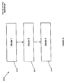
- FIGS. 1, 2, 3, 4, 5, 6, 7 and 8 a system for acquiring environmental data measurements will now be described.
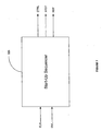
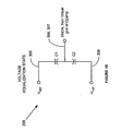
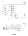
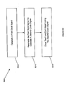
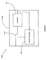
- the system 100 preferably includes a measurement device 105 for detecting environmental data measurements, a controller 110 for controlling the measurement device 105, and a communication interface 115 for coupling the measurement device 105 and the controller 110.
- the measurement device 105 is preferably adapted to detect environmental data measurements.
- the measurement device 105 is coupled to the controller 110 by the communication interface 115.
- the measurement device 105 may include any number of conventional commercially available measurement devices suitable for acquiring environmental data measurements.
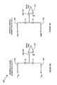
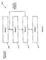
- the measurement device 105 includes a sensor 205, a controller 206, and an interface 207 for coupling the sensor 205 and the controller 206.
- the sensor 205 may include any number of sensors suitable for detecting and recording environmental data measurements such as, for example, a geophone, a hydrophone, a pressure sensor, a temperature sensor, or an accelerometer.
- the sensor 205 is an accelerometer.
- the accelerometer 205 may be micromachined from wafers made from any number of conventional commercially available materials suitable for creating a sensor, such as, for example, silicon, polysilicon, germanium, quartz, pyrex, gallium arsenide, gallium phosphate, or plated metals.
- the accelerometer 205 is micromachined from silicon.
- the design of the sensor 205 is preferably provided substantially as described in United States patent application serial number , attorney docket number 14737.737, filed on , and as described in United States patent number 5,852,242, the disclosures of which are incorporated herein by reference.
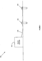
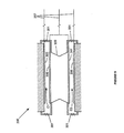
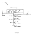
- the sensor 205 includes conductive plates 305, 306, 307, and 308, a measurement mass 309, and springs 301 for supporting the measurement mass 309 within the sensor 205.
- the conductive plates 305, 306, 307, and 308 are substantially identical.
- the plates 305, 306, 307, and 308 may be formed from any number of conventional commercially available materials suitable for forming conductive plates.
- the plates 305, 306, 307, and 308 are provided substantially as described in one or more of the following: United States Patent number 5,852,242, United States Patent number 5,652,384, United States Patent number 5,777,226, and United States patent application serial number , attorney docket number 14737.737, filed on , the disclosures of which are incorporated herein by reference.
- the plates 305, 306, 307, and 308 may be arranged within the sensor 205 in any manner suitable for initiating the interaction between the plates 305, 306, 307, and 308 necessary to create a sensor.
- the plate 305 is positioned substantially opposite the plate 306 and the plate 307 is positioned substantially opposite the plate 308.
- the measurement mass 309 may be formed from any number of conventional commercially available materials, such as, for example, silicon, polysilicon, germanium, quartz, pyrex, gallium arsenide, gallium phosphate, or plated metals. In a preferred embodiment, the measurement mass 309 is micromachined from silicon.
- the springs 301 are preferably adapted to couple the measurement mass 309 to the sensor 205 and to support the measurement mass 309 within the sensor 205.
- the springs 301 preferably further provide electrical connections between the measurement mass 309 and the sensor 205.
- the design of the springs 301 is preferably provided substantially as described in one or more of the following: United States Patent number 5,652,384 and United States Patent number 5,777,226, the disclosures of which are incorporated herein by reference.
- the controller 206 may include any number of controllers suitable for controlling the operation of the sensor 205, such as, for example, a frequency/amplitude modulation controller or an application specific integrated circuit (ASIC).
- the controller 206 is an ASIC.
- the controller 206 is a sigma-delta ASIC controller.
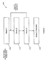
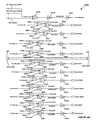
- the controller 206 includes a front-end circuit 310, a loop filter circuit 315, a multiphase clock generator 320, a startup sequencer 325, a sensor simulator 330, and an overload detection device 335.
- the front-end circuit 310 interfaces to the sensor 205 and is adapted to provide electrostatic forcing and position sensing for the measurement mass 309 within the sensor 205.
- the front-end circuit 310 is operably coupled to the sensor 205 by the interface 207.
- the front-end circuit 310 is also preferably operably coupled to the loop filter 315, the multiphase clock generator 320, and the sensor simulator 330.
- the front-end circuit 310 may include any number of circuits suitable for providing electrostatic forcing and position sensing for the sensor 205.
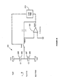
- the front-end circuit 310 is an analog circuit. As illustrated in FIG.
- the front-end circuit 310 preferably includes switches phsu1, phsu2, phu1, phu2, phd1, phd2, phg1, phtc, phbc, phg2, phsg, phs, phf, phloop; phsim, phxbuf, phz, and pha for connecting the sensor 205 to a variety of voltage sources, and a sense amplifier 405 for sensing the position of the measurement mass 309 within the sensor 205.
- the switches phsu1, phsu2, phu1, phu2, phd1, phd2, phg1, phtc, phbc, phg2, phsg, phs, phf, phloop, phsim, phxbuf, phz, and pha may be any number of conventional commercially available switches suitable for connecting the sensor 205 to a variety of voltage sources.
- the sense amplifier 405 may be any number of sense amplifiers suitable for sensing the position of the measurement mass 309 in the sensor 205.
- the sense amplifier 405 is a switched-capacitor circuit.
- the output Vx of the sense amplifier 405 in the front-end circuit 310 is a voltage representing the position of the measurement mass 309 within the sensor 205.
- the position of the measurement mass 309 within the sensor 205 may be representative of the amount of an acceleration force experienced by the measurement mass 309.
- the loop filter 315 is preferably adapted to receive the output Vx from the sense amplifier 405 and create output streams for providing feedback loop compensation and noise shaping for the sensor 205.
- the loop filter 315 is operably coupled to the front-end circuit 310, the multiphase clock generator 320, the startup sequencer 325, and the overload detection device 335.
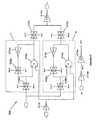
- the loop filter 315 includes one or more integrators 505, a derivative controller 510, a proportional controller 515, summers 520 and 525, a comparator 530, a buffer 535, and scaling devices 507.
- the loop filter 315 is an analog circuit.
- the integrators 505 are used to provide control to the sensor 205.
- the integrators 505 preferably generate third, fourth, and fifth integral terms for fifth-order noise shaping of 1-bit quantization noise.
- the integrators 505 may include any number of conventional commercially available integrators suitable for providing integral control to sensor 205.
- the integrators 505 are switched-capacitor circuits.
- the scaling devices 507 preferably scale the output streams from the integrators 505.
- the scaling devices 507 may be any number of devices suitable for scaling the output streams from the integrators 505.
- the scaling devices 507 are switched-capacitor circuits.
- the derivative controller 510 preferably provides derivative control to the sensor 205.
- the derivative controller 510 provides derivative control to the sensor 205 by generating a velocity term as the first integral of acceleration by using a derivative of the x-position of the measurement mass 309 within the sensor 205.
- the derivative controller 510 may be any number of conventional commercially available controllers suitable for providing derivative control to the sensor 205.
- the derivative controller 510 is a switched-capacitor circuit.
- the proportional controller 515 preferably provides additional control to the sensor 205.
- the proportional controller 515 provides proportional control to the sensor 205 by generating a displacement term as a second integral of the acceleration force experienced by the sensor 205.
- the proportional controller 515 may be any number of conventional commercially available controllers suitable for providing proportional control to the sensor 205.
- the proportional controller 515 is a switched-capacitor circuit.
- the summers 520 preferably receive the output streams from the integrators 505 and combine the streams into a single output data stream. In a preferred embodiment, the summers 520 receive the scaled output streams from the scaling devices 507 and combine them into a single output data stream. In a preferred embodiment, the output data streams from the summers 520 are sent to the next integrator 505.
- the summers 520 may be any number of conventional commercially available devices suitable for combining data streams from the integrators 505 into a single output data stream. In a preferred embodiment, the summers 520 are switched-capacitor circuits.
- the summer 525 preferably receives the output streams from the scaling devices 507, the derivative controller 510, and the proportional controller 515 and combines the streams into a single output data stream.
- the output data stream from the summer 525 drives the comparator 530.
- the output from the summer 525 drives the buffer 535.
- the summer 525 may be any number of conventional commercially available devices suitable for combining data streams from the scaling devices 507, the derivative controller 510, and the proportional controller 515 into a single output data stream.
- the summer 525 is a switched-capacitor circuit.
- the comparator 530 preferably provides a feedback signal to the front-end circuit 310 when the system 100 is operating in a normal sigma-delta operating mode.
- the output stream IMOD from the comparator 530 is a digital 1-bit representation of the output of the loop filter 315.
- the input into the loop filter 315 is the output Vx of the front-end circuit 310, which is representative of the position of the measurement mass 309 within the sensor 205. The position of the measurement mass 309 preferably varies as acceleration forces are applied to the sensor 205.
- the comparator 530 may be any number of conventional commercially available comparators. In a preferred embodiment, the comparator 530 is an analog circuit.
- the buffer 535 preferably provides a feedback signal to the front-end circuit 310 during the start-up of the system 100.
- the output stream Vsum of the buffer 535 is a voltage representation of the acceleration experienced by the sensor 205.
- the input into the loop filter 315 is the output Vx of the front-end circuit 310, which is representative of the position of the measurement mass 309 within the sensor 205.
- the buffer 535 may include any number of conventional commercially available buffers. In a preferred embodiment, the buffer 535 is an analog circuit.
- the multiphase clock generator 320 is adapted to receive input data streams and convert the input streams to output clock signals used to control the switches in the front-end circuit 310 and the loop filter 315.
- the input streams received by the multiphase clock generator 320 may include, for example, the output stream IMOD from the loop filter 315, an external test signal XTST, a test stream TEST designed to combine with the output stream IMOD from the loop filter 315 if the value of the external test signal XTST is high, a master clock signal CLK, and a control signal CTRL for indicating the operating mode of the sensor 205.
- the output stream IMOD from the loop filter 315 an external test signal XTST
- a test stream TEST designed to combine with the output stream IMOD from the loop filter 315 if the value of the external test signal XTST is high
- a master clock signal CLK a master clock signal
- CTRL control signal
- the multiphase clock generator 320 is operably coupled to the front-end circuit 310, the loop filter 315, the startup sequencer 325, and the sensor simulator 330.
- the multiphase clock generator 320 may be any number of conventional commercially available clock generators suitable for controlling switches in the front-end circuit 310 and the loop filter 315.
- the multiphase clock generator 320 is a digital circuit.
- the startup sequencer 325 is preferably adapted to provide stability to the sensor 205 during the start-up of the system 100.
- the startup sequencer 325 is also preferably used to help the sensor 205 handle high-level inputs and recover from unexpected overloads.
- the startup sequencer 325 controls the different modes of operation used by the controller 206 for startup and calibration of the sensor 205.
- the startup sequencer 325 is operably coupled to the loop filter 315, the multiphase clock generator 320, the sensor simulator 330, and the overload detection device 335.
- the input streams into the startup sequencer 325 are the master clock signal CLK and an overload detection signal OVL.
- the output streams from the startup sequencer 325 are preferably the control signal CTRL for indicating the operating mode of the sensor 205, the digital signal XTST for indicating that the controller 206 should use an external test bitstream, and a reset signal RST for resetting the integrators 505 in the loop filter 315, the sense amplifier 405 in the front-end circuit 310, and the multiphase clock generator 320.
- the startup sequencer 325 may be any number of conventional commercially available circuits suitable for helping the sensor 205 handle high-level inputs and recover from unexpected overloads. In a preferred embodiment, the startup sequencer 325 is a digital circuit.
- the sensor simulator 330 is preferably used to substantially duplicate the performance characteristics of the sensor 205 in order to test the operation of the controller 206.
- the sensor simulator 330 is operably coupled to the front-end circuit 310, the multiphase clock generator 320, and the startup sequencer 325.
- the sensor simulator 330 may be any number of devices suitable for duplicating the performance characteristics of the sensor 205 such as, for example, operational amplifiers, capacitors, switches, resistors, or transistors.
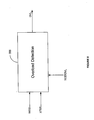
- the overload detection device 335 preferably provides detection of high level inputs and system 100 overloads.
- the overload detection device 335 is operably coupled to the loop filter 315 and the startup sequencer 325.
- the input streams into the overload detection device 335 may include, for example, the output stream IMOD from the loop filter 315, the external test stream XTST, and a test overload signal TESTOVL.
- the output stream OVL from the overload detection device is preferably sent to the startup sequencer 325 when an overload in the system 100 has been detected.
- the overload detection device 335 may be any number of conventional commercially available devices suitable for providing overload detection for the controller 206.
- the overload detection device 335 is a digital counter circuit.
- the interface 207 couples the sensor 205 to the controller 206.
- the interface 207 may be any number of conventional commercially available interfaces suitable for coupling the sensor 205 and the controller 206 such as, for example, fiber optics or wireless telemetry.
- the interface 207 includes electrical cables extending from the conductive plates 305, 306, 307, and 308 positioned within the sensor 205.
- the conductive plate 306 is positioned within the sensor 205 on a top surface of the measurement mass 309, substantially opposite the conductive plate 305.
- the conductive plates 305 and 306 preferably interact to form a variable capacitor C1 within the sensor 205.
- conductive plate 307 is positioned within the sensor 205 on a bottom surface of the measurement mass 309, substantially opposite the conductive plate 308.
- the conductive plates 307 and 308 preferably interact to form a variable capacitor C2 within the sensor 205.
- the front-end circuit 310 interacts with the sensor 205 to place the sensor 205 in a variety of operating states.
- the different operating states into which the sensor 205 is placed preferably include (1) a DUMMY FORCE DOWN STATE, (2) a DUMMY FORCE UP STATE, (3) a FIRST MODULATOR FORCE UP STATE, (4) a SECOND MODULATOR FORCE UP STATE, (5) a FIRST MODULATOR FORCE DOWN STATE, (6) a SECOND MODULATOR FORCE DOWN STATE, (7) a RETURN-TO-ZERO STATE, (8) a GRAVITY CANCELLATION STATE, (9) a VOLTAGE EQUALIZATION STATE, (10) a SENSING (CHARGE SUMMATION) STATE 1, and (11) a SENSING STATE 2.
- the controller 206 places the sensor 205 in the DUMMY FORCE DOWN STATE by applying a negative reference voltage -V ref to conductive plates 305, 306 and 307 and a positive reference voltage +V ref to conductive plate 308.
- the negative reference voltage -V ref is preferably applied to the conductive plates 305, 306, and 307 by turning on switches phd1 and phtc to connect the plates 305, 306, and 307 to the negative reference voltage -V ref source.
- the positive reference voltage +V ref is preferably applied to conductive plate 308 by turning on switch phd2 to connect plate 308 to the positive reference voltage +V ref source.
- the positive reference voltage +V ref on conductive plate 308 combined with the negative reference voltage -V ref on plate 307 on the measurement mass 309 preferably results in an electrostatic attraction between the measurement mass 309 and the conductive plate 308.
- the net effect of the attractive forces created within the sensor 205 is to apply an electrostatic force on the measurement mass 309.
- the electrostatic force applies a downward force to the measurement mass 309 during the DUMMY FORCE DOWN STATE.
- the controller 206 places the sensor 205 in the DUMMY FORCE UP STATE by applying a positive reference voltage +V ref to conductive plate 305 and a negative reference voltage -V ref to conductive plates 306, 307, and 308.
- the positive reference voltage +V ref is preferably applied to the conductive plate 305 by turning on switch phu1 to connect the plate 305 to the positive reference voltage +V ref source.
- the negative reference voltage -V ref is preferably applied to conductive plates 306, 307, and 308 by turning on switches phu2 and phbc to connect plates 306, 307, and 308 to the negative reference voltage -V ref source.
- the positive reference voltage +V ref on conductive plate 305 combined with the negative reference voltage -V ref on plate 306 on the measurement mass 309 preferably results in an electrostatic attraction between the measurement mass 309 and the conductive plate 305.
- the net effect of the attractive forces created within the sensor 205 is to apply an electrostatic force on the measurement mass 309.
- the electrostatic force applies an upward force to the measurement mass 309 during the DUMMY FORCE UP STATE.
- the controller 206 places the sensor 205 in the FIRST MODULATOR FORCE UP STATE during the normal sigma-delta operating mode by applying a positive reference voltage + V ref to conductive plate 305 and a negative reference voltage - V ref to conductive plates 306, 307, and 308.
- the controller 206 places the sensor 205 in the FIRST MODULATOR FORCE UP STATE when the output stream IMOD from the loop filter 315 has a negative value.
- the positive reference voltage + V ref is preferably applied to the conductive plate 305 by turning on switch phu1 to connect the plate 305 to the positive reference voltage +V ref source.
- the negative reference voltage -V ref is preferably applied to conductive plates 306, 307, and 308 by turning on switches phu2 and phbc to connect plates 306, 307, and 308 to the negative reference voltage V ref source.
- the positive reference voltage +V ref on conductive plate 305 combined with the negative reference voltage -V ref on plate 306 on the measurement mass 309 preferably results in an electrostatic attraction between the measurement mass 309 and the conductive plate 305.
- the net effect of the attractive forces created within the sensor 205 is to apply an electrostatic force on the measurement mass 309.
- the electrostatic force applies an upward force to the measurement mass 309 during the FIRST MODULATOR FORCE UP STATE.
- the controller 206 places the sensor 205 in the SECOND MODULATOR FORCE UP STATE during system 100 start-up by applying a voltage V DDA to conductive plate 305, applying a voltage V SSA to conductive plate 308, and applying the output Vsum from the reduced-order loop filter 315 to plates 306 and 307 on the measurement mass 309.
- the controller 206 places the sensor 205 in the SECOND MODULATOR FORCE UP STATE when the output stream Vsum from the reduced-order loop filter 315 has a value of less than zero volts.
- the voltage V DDA is preferably applied to the conductive plate 305 by turning on switch phsu1 to connect the plate 305 to the voltage V DDA source.
- the voltage V SSA is preferably applied to conductive plate 308 by turning on switch phsu2 to connect plate 308 to the voltage V SSA source.
- the voltage Vsum is preferably applied to plates 306 and 307 by turning on switch phloop to connect plates 306 and 307 to the output Vsum from the reduced-order loop filter 315.
- the net attractive forces may, for example, move the measurement mass 309 upwards or downwards.
- the net effect of the attractive forces created within the sensor 205 is to apply a net force upward on the measurement mass 309 during the SECOND MODULATOR FORCE UP STATE.
- the amount of upward force applied to the measurement mass 309 preferably depends on the level of the voltage Vsum ( ⁇ 0 V).
- the controller 206 places the sensor 205 in the FIRST MODULATOR FORCE DOWN STATE during normal sigma-delta operating mode by applying a negative reference voltage -V ref to conductive plate 305, 306 and 307 and a positive reference voltage +V ref to conductive plate 308.
- the controller 206 places the sensor 205 in the FIRST MODULATOR FORCE DOWN STATE when the output stream IMOD from the loop filter 315 has a positive value.
- the negative reference voltage -V ref is preferably applied to the conductive plates 305, 306, and 307 by turning on switches phd1 and phtc to connect the plates 305, 306, and 307 to the negative reference voltage -V ref source.
- the positive reference voltage +V ref is preferably applied to conductive plate 308 by turning on switch phd2 to connect plate 308 to the positive reference voltage +V ref source.
- the positive reference voltage + V ref on conductive plate 308 combined with the negative reference voltage -V ref on plate 307 on the measurement mass 309 preferably results in an electrostatic attraction between the measurement mass 309 and the conductive plate 308.
- the net effect of the attractive forces created within the sensor 205 is to apply an electrostatic force on the measurement mass 309.
- the electrostatic force applies a downward force to the measurement mass 309 during the FIRST MODULATOR FORCE DOWN STATE.
- the controller 206 places the sensor 205 in the SECOND MODULATOR FORCE DOWN STATE during system 100 start-up by applying a voltage V DDA to conductive plate 305, applying a voltage V SSA to conductive plate 308, and applying the output Vsum from the loop filter 315 to plates 306 and 307 on the measurement mass 309.
- the controller 206 places the sensor 205 in the SECOND MODULATOR FORCE DOWN STATE when the output stream Vsum from the reduced-order loop filter 315 has a value of greater than zero volts.
- the voltage V DDA is preferably applied to the conductive plate 305 by turning on switch phsu1 to connect the plate 305 to the voltage V DDA source.
- the voltage V SSA is preferably applied to conductive plate 308 by turning on switch phsu2 to connect plate 308 to the voltage V SSA source.
- the voltage Vsum is preferably applied to plates 306 and 307 by turning on switch phloop to connect plates 306 and 307 to the output Vsum of the reduced-order loop filter 315.
- the net attractive forces may, for example, move the measurement mass 309 upwards or downwards.
- the net effect of the attractive forces created within the sensor 205 is to apply a net force downward on the measurement mass 309 during the SECOND MODULATOR FORCE DOWN STATE.
- the amount of downward force applied to the measurement mass 309 preferably depends on the level of the voltage Vsum (>0 V).
- the controller 206 places the sensor 205 in a RETURN-TO-ZERO STATE by grounding the conductive plates 305, 306, 307, and 308 to reduce signal dependent current draw from reference sources.
- the conductive plate 305 is grounded by turning on switch phg1 to connect the conductive plate 305 to a grounding source.
- conductive plates 306 and 307 are grounded by turning on switch phsg to connect the conductive plates 306 and 307 to a grounding source.
- the conductive plate 308 is grounded by turning on switch phg2 to connect the conductive plate 308 to a grounding source.
- the charges across capacitors C1 and C2 are preferably equal to zero.
- no net electrostatic force is applied to the measurement mass 309 in the RETURN-TO-ZERO STATE.
- the controller 206 places the sensor 205 in the GRAVITY CANCELLATION STATE by applying a positive reference voltage +V ref to plate 305, applying a negative reference voltage -V ref to plate 308, and applying a voltage V dac or V sum on plates 306 and 307.
- the positive reference voltage +V ref is preferably applied to plate 305 by turning on switch phu1 to connect the conductive plate 305 to the positive reference voltage +V ref source.
- the negative reference voltage -V ref is preferably applied to the conductive plate 308 by turning on switch phu2 to connect the conductive plate 308 to the negative reference voltage -V ref source.
- the voltage V dac is preferably applied to the conductive plates 306 and 307 by turning on switch phf to connect the conductive plates 306 and 307 to a voltage V dac source.
- the voltage V sum is preferably applied to the conductive plates 306 and 307 by turning on switch phloop to connect the conductive plates 306 and 307 to a voltage V sum source.
- the positive reference voltage + V ref on conductive plate 305 combined with the voltage V dac or V sum on the conductive plates 306 and 307 preferably results in an electrostatic attraction between the measurement mass 309 and the conductive plate 305.
- the negative reference voltage -V ref on the conductive plate 308 combined with the voltage V dac or V sum on the conductive plates 306 and 307 preferably results in an electrostatic attraction between the measurement mass 309 and the conductive plate 308.
- the net effect of the attractive forces created within the sensor 205 is to apply an electrostatic force on the measurement mass 309.
- the electrostatic force created by the attractive forces may, for example, move the measurement mass 309 upwards or downwards.
- the electrostatic force on the measurement mass 309 during the GRAVITY CANCELLATION STATE substantially cancels a 1-g static field experienced by the sensor 205.
- the controller 206 places the sensor 205 in the VOLTAGE EQUALIZATION STATE by applying a positive reference voltage +V ref to the plate 305, applying a negative reference voltage -V ref to the plate 308, and by sequentially grounding the plates 306 and 307 to dissipate charges on the plates 306 and 307 and then connecting the plates 306 and 307 to the sense amplifier 405.
- the sense amplifier 405 input offset voltage is preferably stored for subsequent cancellation.
- the positive reference voltage +V ref is preferably applied to the plate 305 by turning on switch phu1 to connect the conductive plate 305 to the positive reference voltage +V ref source.
- the negative reference voltage -V ref is preferably applied to the conductive plate 308 by turning on switch phu2 to connect the conductive plate 308 to the negative reference voltage -V ref source.
- the conductive plates 306 and 307 are grounded by turning on switch phsg to connect the conductive plates 306 and 307 to a grounding source.
- the voltage equal to the offset of the sense amplifier is applied to the plates 306 and 307 by turning on switch phs to connect the conductive plates 306 and 307 to the sense amplifier 405.
- the conductive plates 306 and 307 are initially grounded while the positive reference voltage +V ref is applied to plate 305 and the negative reference voltage -V ref is applied to the conductive plate 308. In a preferred embodiment, no electrostatic forces are applied to the sensor 205 and the charges across capacitors C1 and C2 are preferably substantially equal.
- the voltage equal to the offset of the sense amplifier 405 is applied to the plates 306 and 307 while the positive reference voltage +V ref is applied to plate 305 and the negative reference voltage -V ref is applied to the conductive plate 308.
- electrostatic forces are preferably applied to the sensor 205. The electrostatic forces alter the charges across capacitors C1 and C2. The magnitude of the variation in charges across capacitors C1 and C2 depends on the magnitude of the offset voltage of the sense amplifier 405.
- the controller 206 places the sensor 205 in the SENSING STATE 1 (CHARGE SUMMATION STATE) by applying the negative reference voltage -V ref to the conductive plate 305, applying the positive reference voltage +V ref to the conductive plate 308, and connecting the sense amplifier 405 to the conductive plates 306 and 307.
- the controller 206 places the sensor 205 in the SENSING STATE 1 following the VOLTAGE EQUALIZATION STATE.
- the charge differential on capacitors C1 and C2 is measured to determine the position of the measurement mass 309 within the sensor 205.
- the negative reference voltage -V ref is applied to plate 305
- the positive reference voltage +V ref is applied to plate 308, and the plates 306 and 307 are connected to the sense amplifier 405.
- the negative reference voltage -V ref is preferably applied to the plate 305 by turning on switch phd1 to connect the plate 305 to the negative reference voltage -V ref source.
- the positive reference voltage +V ref is preferably applied to the plate 308 by turning on switch phd2 to connect the plate 308 to the positive reference voltage +V ref source.
- the plates 306 and 307 are preferably connected to the sense amplifier by turning on switch phs to connect the plates 306 and 307 to the inverting terminal of the sense amplifier 405.
- the controller 206 places the sensor 205 in the SENSING STATE 2 by grounding plates 305 and 308 while connecting plates 306 and 307 to inverting terminal of the sense amplifier 405.
- the controller 206 preferably grounds plate 305 by turning on switch phg1 to connect the plate 305 to the grounding source.
- the controller 206 preferably grounds plate 308 by turning on switch phg2 to connect the plate 308 to the grounding source.
- the controller 206 preferably connects plates 306 and 307 to the sense amplifier 405 by turning on switch phs.
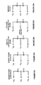
- the DUMMY FORCE DOWN STATE, the DUMMY FORCE UP STATE, the FIRST MODULATOR FORCE UP STATE, the SECOND MODULATOR FORCE UP STATE, the FIRST MODULATOR FORCE DOWN STATE, the SECOND MODULATOR FORCE DOWN STATE, the RETURN-TO-ZERO STATE, the GRAVITY CANCELLATION STATE, the VOLTAGE EQUALIZATION STATE, the SENSING STATE 1 and the SENSING STATE 2 may be used in any combination to create any number of operating modes for the sensor 205. Each operating mode is preferably implemented by setting up a forcing pattern during sixteen clock periods of a 2 MHZ clock.
- the sixteen clock periods of the 2 MHZ clock are broken down into thirty-two half-periods.
- the forcing pattern is repeated periodically at 128 kHz.
- the sensor 205 experiences four types of operating modes under the control of the controller 206: a measurement mass 309 setup operating mode (OPERATING MODE 1), a gravity cancellation operating mode (OPERATING MODE 2), a stray capacitance calibration operating mode (OPERATING MODE 3), and a sigma-delta operating mode (OPERATING MODE 4).
- the gravity cancellation mode (OPERATING MODE 2) and the stray capacitance calibration mode (OPERATING MODE 3) preferably work together to cancel the effects of gravity and stray capacitances on the sensor 205.
- the controller 206 preferably pulls the measurement mass 309 off stops within the sensor 205 and positions the measurement mass 309 so that capacitors C1 and C2 are substantially equal.
- the controller 206 may utilize any of the eleven generic operating states described above, and variations thereof, to create the OPERATING MODE 1.
- the controller 206 places the sensor 205 in the MODULATOR FORCING STATE, the VOLTAGE EQUALIZATION STATE, and the SENSING STATE during the OPERATING MODE 1.
- the controller 206 initially interacts with the sensor 205 to place the sensor 205 in one of the modulator forcing states.
- the system 100 is preferably operating in start-up mode, and the loop filter 315 is operating in reduced-order mode. Therefore, the controller 206 preferably places the sensor 205 in either the SECOND MODULATOR FORCE UP STATE or the SECOND MODULATOR FORCE DOWN STATE, depending on the value of the output Vsum of the reduced-order loop filter 315.
- the controller 206 may place the sensor 205 in the SECOND MODULATOR FORCE UP STATE or the SECOND MODULATOR FORCE DOWN STATE for any number of the sixteen clock periods within the operating cycle.
- the controller 206 places the sensor 205 in the SECOND MODULATOR FORCE UP STATE or the SECOND MODULATOR FORCE DOWN STATE for clock periods 1 through 14 of the OPERATING MODE 1.
- the controller 206 preferably places the sensor 205 in the VOLTAGE EQUALIZATION STATE.
- the controller 206 may place the sensor 205 in the VOLTAGE EQUALIZATION STATE for any number of the sixteen clock periods within the operating cycle.
- the controller 206 places the sensor 205 in the voltage equalization state during clock period 15 of the OPERATING MODE 1.
- the controller 206 preferably completes the OPERATING MODE 1 by placing the sensor 205 in the SENSING STATE 2.
- the controller 206 may place the sensor 205 in the SENSING STATE 2 for any number of the sixteen clock periods within the operating cycle.
- the controller 206 places the sensor 205 in the SENSING STATE 2 during clock period 16 of the OPERATING MODE 1.
- the controller 206 preferably cancels the effects of gravitational forces on the sensor 205 and calibrates the voltage V DAC applied to plates 306 and 307 during normal sigma-delta mode so that the operating range of the sensor 205 is approximately +/-0.1g. Also, during the OPERATING MODE 2, the voltage Vsum is digitized for use during the stray capacitance calibration of the OPERATING MODE 3.
- the controller 206 may utilize any of the eleven generic operating states, or variations thereof, to create the OPERATING MODE 2. In a preferred embodiment, as illustrated in FIGS.
- the controller 206 places the sensor 205 in the RETURN-TO-ZERO STATE, the GRAVITY CANCELLATION STATE, the VOLTAGE EQUALIZATION STATE, and the SENSING STATE 1 during the OPERATING MODE 2.
- the controller 206 begins the OPERATING MODE 2 by placing the sensor 205 in the RETURN-TO-ZERO STATE to remove any charges from the conductive plates 305, 306, 307, and 308.
- the controller 206 may place the sensor 205 in the RETURN-TO-ZERO STATE for any number of the sixteen clock periods within the OPERATING MODE 2.
- the controller 206 places the sensor 205 in the RETURN-TO-ZERO STATE for clock periods 1 through 4 of the OPERATING MODE 2.
- the controller 206 preferably places the sensor 205 in the GRAVITY CANCELLATION STATE to cancel the effects of the 1-g static field from within the sensor 205.
- the controller 206 may place the sensor 205 in the GRAVITY CANCELLATION STATE for any number of the sixteen clock periods within the OPERATING MODE 2.
- the controller 206 places the sensor 205 in the GRAVITY CANCELLATION STATE for the clock periods 5 through 12 of the OPERATING MODE 2.
- the controller 206 preferably places the sensor 205 in the VOLTAGE EQUALIZATION STATE to equalize the voltage across capacitors C1 and C2 within the sensor 205.
- the controller 206 may place the sensor 205 in the VOLTAGE EQUALIZATION STATE for any number of the sixteen clock periods within the OPERATING MODE 2.
- the controller 206 places the sensor 205 in the VOLTAGE EQUALIZATION STATE for clock periods 13 and 14 of the OPERATING MODE 2.
- the controller 206 preferably places the sensor 205 in the SENSING STATE 1.
- the controller 206 may place the sensor 205 in the SENSING STATE 1 for any number of the sixteen clock periods within the OPERATING MODE 2.
- the controller 206 places the sensor 205 in the SENSING STATE 1 for clock periods 15 and 16 of the OPERATING MODE 2.
- the controller 206 cancels the effects of stray capacitances within the sensor 205 during the OPERATING MODE 3.
- the controller 206 utilizes the digitized voltage Vsum from the OPERATING MODE 2 during the stray capacitance calibration of the OPERATING MODE 3.
- the stray capacitance calibration is performed substantially as described in United States patent application serial number 09/268,072, attorney docket number 456020.12-IOS12, filed on 3/12/1999, the disclosure of which is incorporated herein by reference.
- the performance of the sensor 205 may be affected, for example, by external factors known as stray capacitances.
- Stray capacitances may be caused by any number of sources, but two mechanisms typically responsible for the stray capacitances are process variations within or internal to the sensor 205 and the sensor 205 package, and external effects related to socketing PC board layout. As illustrated in FIG. 22, the external stray capacitances are lumped together and denoted as C1se and C2se, and the internal stray capacitances are lumped together and denoted as C1si and C2si.
- the controller 206 preferably utilizes the effects of the OPERATING MODE 2 to calibrate the voltage Vdac for 1-g cancellation and to cancel the effects of stray capacitances within the sensor 205.
- the controller 206 may utilize any of the eleven generic operating states described above, or variations thereof, to create the OPERATING MODE 3.
- the controller 206 places the sensor 205 in the DUMMY FORCE DOWN STATE, the DUMMY FORCE UP STATE, the GRAVITY CANCELLATION STATE, the VOLTAGE EQUALIZATION STATE, and the SENSING STATE 1 during the OPERATING MODE 3.
- the controller 206 begins the OPERATING MODE 3 by placing the sensor 205 in the DUMMY FORCE DOWN STATE to force the measurement mass 309 down away from plate 305 towards plate 308.
- the controller 206 may place the sensor 205 in the DUMMY FORCE DOWN STATE for any number of the sixteen clock periods within the OPERATING MODE 3.
- the controller 206 places the sensor 205 in the DUMMY FORCE DOWN STATE for clock periods 1 and 2 of the OPERATING MODE 3.
- the controller 206 preferably places the sensor 205 in the DUMMY FORCE UP STATE to force the measurement mass 309 up away from plate 308 and towards plate 305.
- the controller 206 may place the sensor 205 in the DUMMY FORCE UP STATE for any number of the sixteen clock periods within the OPERATING MODE 3.
- the controller 206 places the sensor 205 in the DUMMY FORCE UP STATE for clock periods 3 and 4 of the OPERATING MODE 3.
- the controller 206 preferably places the sensor 205 in the GRAVITY CANCELLATION STATE.
- the controller 206 may place the sensor 205 in the GRAVITY CANCELLATION STATE for any number of the sixteen clock periods within the OPERATING MODE 3.
- the controller 206 places the sensor 205 in the GRAVITY CANCELLATION STATE for clock periods 5 through 12 of the OPERATING MODE 3.
- the controller 206 preferably places the sensor 205 in the VOLTAGE EQUALIZATION STATE.
- the controller 206 may place the sensor 205 in the VOLTAGE EQUALIZATION STATE for any number of the sixteen clock periods within the OPERATING MODE 3.
- the controller 206 places the sensor 205 in the VOLTAGE EQUALIZATION STATE for clock periods 13 and 14 of the OPERATING MODE 3.
- the controller 206 preferably completes the OPERATING MODE 3 by placing the sensor 205 in the SENSING STATE 1 to measure the differential charge on capacitors C1 and C2.
- the controller 206 preferably analyzes the differential charges to determine the position of the measurement mass 309 within the sensor 205.
- the differential charges across capacitors C1 and C2 may, for example, be equal or unequal.
- the controller 206 may place the sensor 205 in the SENSING STATE 1 for any number of the sixteen clock periods within the OPERATING MODE 3.
- the controller 206 places the sensor 205 in the SENSING STATE 1 for clock periods 15 and 16 of the OPERATING MODE 3.
- the OPERATING MODE 4 will now be described.
- the sensor 205 preferably operates in a sigma-delta operating mode.
- the controller 206 may alter the arrangement of the eleven generic operating states described above, or variations thereof, to create any number of different sigma-delta operating modes.
- the controller 206 utilizes eight different configurations to create sub-modes of the OPERATING MODE 4, including: (1) a long forcing mode with dummy forces in OPERATING MODE 4.1, (2) a long forcing mode with dummy forces and test bit interleaving in OPERATING MODE 4.2, (3) a short forcing mode with dummy forces in OPERATING MODE 4.3, (4) a long forcing mode with return-to-zero forces in OPERATING MODE 4.4, (5) a long forcing mode with return-to-zero forces and test bit interleaving in OPERATING MODE 4.5, (6) a short forcing mode with return-to-zero forces in OPERATING MODE 4.6, (7) a short forcing mode with return-to-zero forces and test bit interleaving in OPERATING MODE 4.7, and (8) a very long forcing mode with return-to-zero forces in OPERATING MODE 4.8.
- the controller 206 utilizes a long forcing mode with dummy forces during the OPERATING MODE 4.1.
- the controller 206 may utilize any number of the eleven generic operating states described above, or variations thereof, to create the OPERATING MODE 4.1.
- the controller 206 utilizes the DUMMY FORCE DOWN STATE, the FIRST MODULATOR FORCE UP STATE or the FIRST MODULATOR FORCE DOWN STATE, the DUMMY FORCE UP STATE, the GRAVITY CANCELLATION STATE, the VOLTAGE EQUALIZATION STATE, and the SENSING STATE 1 to create the OPERATING MODE 4.1.
- the controller 206 begins the OPERATING MODE 4.1 by placing the sensor 205 in the DUMMY FORCE DOWN STATE to force the measurement mass 309 down away from plate 305 towards plate 308.
- the controller 206 may place the sensor 205 in the DUMMY FORCE DOWN STATE for any number of the sixteen clock periods within the OPERATING MODE 4.1.
- the controller 206 places the sensor 205 in the DUMMY FORCE DOWN STATE for clock period 1 of the OPERATING MODE 4.1.
- the controller 206 preferably places the sensor 205 in the FIRST MODULATOR FORCE UP STATE or the FIRST MODULATOR FORCE DOWN STATE to force the measurement mass 309 as a function of the position of the measurement mass 309 within the sensor 205.
- the controller 206 may place the sensor 205 in the FIRST MODULATOR FORCE UP STATE or the FIRST MODULATOR FORCE DOWN STATE for any number of the sixteen clock periods within the OPERATING MODE 4.1.
- the controller 206 places the sensor 205 in the FIRST MODULATOR FORCE UP STATE or the FIRST MODULATOR FORCE DOWN STATE for clock periods 2 and 3 of the OPERATING MODE 4.1.
- the controller 206 preferably places the sensor 205 in the DUMMY FORCE UP STATE to force the measurement mass 309 up away from plate 308 towards plate 305.
- the controller 206 may place the sensor 205 in the DUMMY FORCE UP STATE for any number of the sixteen clock periods within the OPERATING MODE 4.1.
- the controller 206 places the sensor 205 in the DUMMY FORCE UP STATE for clock period 4 of the OPERATING MODE 4.1.
- the controller 206 preferably places the sensor 205 in the GRAVITY CANCELLATION STATE.
- the controller 206 may place the sensor 205 in the GRAVITY CANCELLATION STATE for any number of the sixteen clock periods within the OPERATING MODE 4.1.
- the controller 206 places the sensor 205 in the GRAVITY CANCELLATION STATE for clock periods 5 through 12 of the OPERATING MODE 4.1.
- the controller 206 preferably places the sensor 205 in the VOLTAGE EQUALIZATION STATE.
- the controller 206 may place the sensor 205 in the VOLTAGE EQUALIZATION STATE for any number of the sixteen clock periods within the OPERATING MODE 4.1.
- the controller 206 places the sensor 205 in the VOLTAGE EQUALIZATION STATE for clock periods 13 and 14 of the OPERATING MODE 4.1.
- the controller 206 preferably places the sensor 205 in the SENSING STATE 1.
- the controller 206 may place the sensor 205 in the SENSING STATE 1 for any number of the sixteen clock periods within the OPERATING MODE 4.1.
- the controller 206 places the sensor 205 in the SENSING STATE 1 for clock periods 15 and 16 of the OPERATING MODE 4.1.
- the controller 206 utilizes a long forcing mode with dummy forces and test interleaving during the OPERATING MODE 4.2.
- the controller 206 may utilize any number of the eleven generic operating states described above, or variations thereof, to create the OPERATING MODE 4.2.
- the controller 206 utilizes the DUMMY FORCE DOWN STATE, the FIRST MODULATOR FORCE UP STATE or the FIRST MODULATOR FORCE DOWN STATE, a test force state, the DUMMY FORCE UP STATE, the GRAVITY CANCELLATION STATE, the VOLTAGE EQUALIZATION STATE, and the SENSING STATE 1 to create the OPERATING MODE 4.2.
- the controller 206 begins the OPERATING MODE 4.2 by placing the sensor 205 in the DUMMY FORCE DOWN STATE to force the measurement mass 309 down away from plate 305 towards plate 308.
- the controller 206 may place the sensor 205 in the DUMMY FORCE DOWN STATE for any number of the sixteen clock periods within the OPERATING MODE 4.2.
- the controller 206 places the sensor 205 in the DUMMY FORCE DOWN STATE for clock period 1 of the OPERATING MODE 4.2.
- the controller 206 preferably places the sensor 205 in the FIRST MODULATOR FORCE UP STATE or the FIRST MODULATOR FORCE DOWN STATE to force the measurement mass 309 as a function of the position of the measurement mass 309 within the sensor 205.
- the controller 206 may place the sensor 205 in the FIRST MODULATOR FORCE UP STATE or the FIRST MODULATOR FORCE DOWN STATE for any number of the sixteen clock periods within the OPERATING MODE 4.2.
- the controller 206 places the sensor 205 in the FIRST MODULATOR FORCE UP STATE or the FIRST MODULATOR FORCE DOWN STATE for clock period 2 of the OPERATING MODE 4.2.
- the controller 206 preferably places the sensor 205 in a test forcing state.
- the controller 206 preferably creates the test state by interleaving a test bit input into the data stream in place of the FIRST MODULATOR FORCE UP STATE or the FIRST MODULATOR FORCE DOWN STATE, depending on the value of the output stream IMOD from the loop filter 315.
- the controller 206 interleaves the test bit stream substantially as described in United States Patent No. 6,023,960, the disclosure of which is incorporated herein by reference.
- the controller 206 may place the sensor 205 in the test forcing state for any number of the sixteen clock periods within the OPERATING MODE 4.2.
- the controller 206 places the sensor 205 in the test forcing state for clock period 3 of the OPERATING MODE 4.2.
- the controller 206 preferably places the sensor 205 in the DUMMY FORCE UP STATE to force the measurement mass 309 up away from plate 308 towards plate 305.
- the controller 206 may place the sensor 205 in the DUMMY FORCE UP STATE for any number of the sixteen clock periods within the OPERATING MODE 4.2.
- the controller 206 places the sensor 205 in the DUMMY FORCE UP STATE for clock period 4 of the OPERATING MODE 4.2.
- the controller 206 preferably places the sensor 205 in the GRAVITY CANCELLATION STATE.
- the controller 206 may place the sensor 205 in the GRAVITY CANCELLATION STATE for any number of the sixteen clock periods within the OPERATING MODE 4.2.
- the controller 206 places the sensor 205 in the GRAVITY CANCELLATION STATE for clock periods 5 through 12 of the OPERATING MODE 4.2.
- the controller preferably places the sensor 205 in the VOLTAGE EQUALIZATION STATE.
- the controller 206 may place the sensor 205 in the VOLTAGE EQUALIZATION STATE for any number of the sixteen clock periods within the OPERATING MODE 4.2.
- the controller 206 places the sensor 205 in the VOLTAGE EQUALIZATION STATE for clock periods 13 and 14 of the OPERATING MODE 4.2.
- the controller 206 preferably places the sensor 205 in the SENSING STATE 1.
- the controller 206 may place the sensor 205 in the SENSING STATE 1 for any number of the sixteen clock periods within the OPERATING MODE 4.2.
- the controller 206 places the sensor 205 in the SENSING STATE 1 for clock periods 15 and 16 of the OPERATING MODE 4.2.
- the controller 206 utilizes a short forcing mode with dummy forces during the OPERATING MODE 4.3.
- the controller 206 may utilize any number of the eleven generic operating states described above, or variations thereof, to create the OPERATING MODE 4.3.
- the controller 206 utilizes the DUMMY FORCE DOWN STATE, the FIRST MODULATOR FORCE UP STATE or the FIRST MODULATOR FORCE DOWN STATE, the DUMMY FORCE UP STATE, the GRAVITY CANCELLATION STATE, the VOLTAGE EQUALIZATION STATE, and the SENSING STATE 1 to create the OPERATING MODE 4.3.
- the controller 206 begins the OPERATING MODE 4.3 by placing the sensor 205 in the DUMMY FORCE DOWN STATE to force the measurement mass 309 down away from plate 305 towards plate 308.
- the controller 206 may place the sensor 205 in the DUMMY FORCE DOWN STATE for any number of the sixteen clock periods within the OPERATING MODE 4.3.
- the controller 206 places the sensor 205 in the DUMMY FORCE DOWN STATE for clock period 1 and the first half of clock period 2 of the OPERATING MODE 4.3.
- the controller 206 preferably places the sensor 205 in the FIRST MODULATOR FORCE UP STATE or the FIRST MODULATOR FORCE DOWN STATE to force the measurement mass 309 as a function of the position of the measurement mass 309 within the sensor 205.
- the controller 206 may place the sensor 205 in the FIRST MODULATOR FORCE UP STATE or the FIRST MODULATOR FORCE DOWN STATE for any number of the sixteen clock periods within the OPERATING MODE 4.3.
- the controller 206 places the sensor 205 in the FIRST MODULATOR FORCE UP STATE or the FIRST MODULATOR FORCE DOWN STATE for the second half of clock period 2 and the first half of clock period 3 within the OPERATING MODE 4.3.
- the controller 206 preferably places the sensor 205 in the DUMMY FORCE UP STATE to force the measurement mass 309 up away from plate 308 towards plate 305.
- the controller 206 may place the sensor 205 in the DUMMY FORCE UP STATE for any number of the sixteen clock periods within the OPERATING MODE 4.3.
- the controller 206 places the sensor 205 in the DUMMY FORCE UP STATE for the second half of clock period 3 and clock period 4 of the OPERATING MODE 4.3.
- the controller 206 preferably places the sensor 205 in the GRAVITY CANCELLATION STATE.
- the controller 206 may place the sensor 205 in the GRAVITY CANCELLATION STATE for any number of the sixteen clock periods within the OPERATING MODE 4.3.
- the controller 206 places the sensor 205 in the GRAVITY CANCELLATION STATE for clock periods 5 through 12 of the OPERATING MODE 4.3.
- the controller 206 preferably places the sensor 205 in the VOLTAGE EQUALIZATION STATE.
- the controller 206 may place the sensor 205 in the VOLTAGE EQUALIZATION STATE for any number of the sixteen clock periods within the OPERATING MODE 4.3.
- the controller 206 places the sensor 205 in the VOLTAGE EQUALIZATION STATE for clock periods 13 and 14 of the OPERATING MODE 4.3.
- the controller 206 preferably places the sensor 205 in the SENSING STATE 1.
- the controller 206 may place the sensor 205 in the SENSING STATE 1 for any number of the sixteen clock periods within the OPERATING MODE 4.3.
- the controller 206 places the sensor 205 in the SENSING STATE 1 for clock periods 15 and 16 of the OPERATING MODE 4.3.
- the controller 206 utilizes a long forcing mode with return-to-zero forces during the OPERATING MODE 4.4.
- the controller 206 may utilize any number of the eleven generic operating states described above, or variations thereof, to create the OPERATING MODE 4.4.
- the controller 206 utilizes the RETURN-TO-ZERO STATE, the FIRST MODULATOR FORCE UP STATE or the FIRST MODULATOR FORCE DOWN STATE, the GRAVITY CANCELLATION STATE, the VOLTAGE EQUALIZATION STATE, and the SENSING STATE 1 to create the OPERATING MODE 4.4.
- the controller 206 begins the OPERATING MODE 4.4 by placing the sensor 205 in the RETURN-TO-ZERO STATE to remove charges from the conductive plates 305, 306, 307, and 308.
- the controller 206 may place the sensor 205 in the RETURN-TO-ZERO STATE for any number of the sixteen clock periods within the OPERATING MODE 4.4.
- the controller 206 places the sensor 205 in the RETURN-TO-ZERO STATE for clock periods 1 and 4 of the OPERATING MODE 4.4.
- the controller 206 preferably places the sensor 205 in the FIRST MODULATOR FORCE UP STATE or the FIRST MODULATOR FORCE DOWN STATE to force the measurement mass 309 as a function of the position of the measurement mass 309 within the sensor 205.
- the controller 206 may place the sensor 205 in the FIRST MODULATOR FORCE UP STATE or the FIRST MODULATOR FORCE DOWN STATE for any number of the sixteen clock periods within the OPERATING MODE 4.4.
- the controller 206 places the sensor 205 in the FIRST MODULATOR FORCE UP STATE or the FIRST MODULATOR FORCE DOWN STATE for clock periods 2 and 3 of the OPERATING MODE 4.4.
- the controller 206 preferably places the sensor 205 in the GRAVITY CANCELLATION STATE.
- the controller 206 may place the sensor 205 in the GRAVITY CANCELLATION STATE for any number of the sixteen clock periods within the OPERATING MODE 4.4.
- the controller 206 places the sensor 205 in the GRAVITY CANCELLATION STATE for clock periods 5 through 12 of the OPERATING MODE 4.4.
- the controller 206 preferably places the sensor 205 in the VOLTAGE EQUALIZATION STATE.
- the controller 206 may place the sensor 205 in the VOLTAGE EQUALIZATION STATE for any number of the sixteen clock periods within the OPERATING MODE 4.4.
- the controller 206 places the sensor 205 in the VOLTAGE EQUALIZATION STATE for clock periods 13 and 14 of the OPERATING MODE 4.4.
- the controller 206 preferably places the sensor 205 in the SENSING STATE 1.
- the controller 206 may place the sensor 205 in the SENSING STATE 1 for any number of the sixteen clock periods within the OPERATING MODE 4.4.
- the controller 206 places the sensor 205 in the SENSING STATE 1 for clock periods 15 and 16 of the OPERATING MODE 4.4.
- the controller 206 utilizes a long forcing mode with return-to-zero forces and test bit interleaving during the OPERATING MODE 4.5.
- the controller 206 may utilize any number of the eleven generic operating states described above, or variations thereof, to create the OPERATING MODE 4.5.
- the controller 206 utilizes the RETURN-TO-ZERO STATE, the FIRST MODULATOR FORCE UP STATE or the FIRST MODULATOR FORCE DOWN STATE, the test forcing state, the GRAVITY CANCELLATION STATE, the VOLTAGE EQUALIZATION STATE, and the SENSING STATE 1 to create the OPERATING MODE 4.5.
- the controller 206 begins the OPERATING MODE 4.5 by placing the sensor 205 in the RETURN-TO-ZERO STATE to remove charges from the conductive plates 305, 306, 307, and 308.
- the controller 206 may place the sensor 205 in the RETURN-TO-ZERO STATE for any number of the sixteen clock periods within the OPERATING MODE 4.5.
- the controller 206 places the sensor 205 in the RETURN-TO-ZERO STATE for clock period 1, the first half of clock period 3, and the second half of clock period 4 of the OPERATING MODE 4.5.
- the controller 206 preferably places the sensor 205 in the FIRST MODULATOR FORCE UP STATE or the FIRST MODULATOR FORCE DOWN STATE to force the measurement mass 309 as a function of the position of the measurement mass 309 within the sensor 205.
- the controller 206 may place the sensor 205 in the FIRST MODULATOR FORCE UP STATE or the FIRST MODULATOR FORCE DOWN STATE for any number of the sixteen clock periods within the OPERATING MODE 4.5.
- the controller 206 places the sensor 205 in the FIRST MODULATOR FORCE UP STATE or the FIRST MODULATOR FORCE DOWN STATE for clock period 2 of the OPERATING MODE 4.5.
- the controller 206 preferably places the sensor 205 in the test forcing state.
- the controller 206 preferably creates the test state by interleaving a test bit input into the data stream in place of the FIRST MODULATOR FORCE UP STATE or the FIRST MODULATOR FORCE DOWN STATE, depending on the value of the output stream IMOD from the loop filter 315.
- the controller 206 interleaves the test bit stream substantially as described in United States Patent No. 6,023,960, the disclosure of which is incorporated herein by reference.
- the controller 206 may place the sensor 205 in the test forcing state for any number of the sixteen clock periods within the OPERATING MODE 4.5.
- the controller 206 places the sensor 205 in the test forcing state for the second half of clock period 3 and the first half of clock period 4 of the OPERATING MODE 4.5.
- the controller 206 preferably places the sensor 205 in the GRAVITY CANCELLATION STATE.
- the controller 206 may place the sensor 205 in the GRAVITY CANCELLATION STATE for any number of the sixteen clock periods within the OPERATING MODE 4.5.
- the controller 206 places the sensor 205 in the GRAVITY CANCELLATION STATE for clock periods 5 through 12 of the OPERATING MODE 4.5.
- the controller 206 preferably places the sensor 205 in the VOLTAGE EQUALIZATION STATE.
- the controller 206 may place the sensor 205 in the VOLTAGE EQUALIZATION STATE for any number of the sixteen clock periods within the OPERATING MODE 4.5.
- the controller 206 places the sensor 205 in the VOLTAGE EQUALIZATION STATE for clock periods 13 and 14 of the OPERATING MODE 4.5.
- the controller 206 preferably places the sensor 205 in the SENSING STATE 1.
- the controller 206 may place the sensor 205 in the SENSING STATE 1 for any number of the sixteen clock periods within the OPERATING MODE 4.5.
- the controller 206 places the sensor 205 in the SENSING STATE 1 for clock periods 15 and 16 of the OPERATING MODE 4.5.
- the controller 206 utilizes a short forcing mode with return-to-zero forces during the OPERATING MODE 4.6.
- the controller 206 may utilize any number of the eleven generic operating states described above, or variations thereof, to create the OPERATING MODE 4.6.
- the controller 206 utilizes the RETURN-TO-ZERO STATE, the FIRST MODULATOR FORCE UP STATE or the FIRST MODULATOR FORCE DOWN STATE, the GRAVITY CANCELLATION STATE, the VOLTAGE EQUALIZATION STATE, and the SENSING STATE 1 to create the OPERATING MODE 4.6.
- the controller 206 begins the OPERATING MODE 4.6 by placing the sensor 205 in the RETURN-TO-ZERO STATE to remove charges from the conductive plates 305, 306, 307, and 308.
- the controller 206 may place the sensor 205 in the RETURN-TO-ZERO STATE for any number of the sixteen clock periods within the OPERATING MODE 4.6.
- the controller 206 places the sensor 205 in the RETURN-TO-ZERO STATE for clock periods 1, 3 and 4 of the OPERATING MODE 4.6.
- the controller 206 preferably places the sensor 205 in the FIRST MODULATOR FORCE UP STATE or the FIRST MODULATOR FORCE DOWN STATE to force the measurement mass 309 as a function of the position of the measurement mass 309 within the sensor 205.
- the controller 206 may place the sensor 205 in the FIRST MODULATOR FORCE UP STATE or the FIRST MODULATOR FORCE DOWN STATE for any number of the sixteen clock periods within the OPERATING MODE 4.6.
- the controller 206 places the sensor 205 in the FIRST MODULATOR FORCE UP STATE or the FIRST MODULATOR FORCE DOWN STATE for clock period 2 of the OPERATING MODE 4.6.
- the controller 206 preferably places the sensor 205 in the GRAVITY CANCELLATION STATE.
- the controller 206 may place the sensor 205 in the GRAVITY CANCELLATION STATE for any number of the sixteen clock periods within the OPERATING MODE 4.6.
- the controller 206 places the sensor 205 in the GRAVITY CANCELLATION STATE for clock periods 5 through 12 of the OPERATING MODE 4.6.
- the controller 206 preferably places the sensor 205 in the VOLTAGE EQUALIZATION STATE.
- the controller 206 may place the sensor 205 in the VOLTAGE EQUALIZATION STATE for any number of the sixteen clock periods within the OPERATING MODE 4.6.
- the controller 206 places the sensor 205 in the VOLTAGE EQUALIZATION STATE for clock periods 13 and 14 of the OPERATING MODE 4.6.
- the controller 206 preferably places the sensor 205 in the SENSING STATE 1.
- the controller 206 may place the sensor 205 in the SENSING STATE 1 for any number of the sixteen clock periods within the OPERATING MODE 4.6.
- the controller 206 places the sensor 205 in the SENSING STATE 1 for clock periods 15 and 16 of the OPERATING MODE 4.6.
- the controller 206 utilizes a short forcing mode with return-to-zero forces and test bit interleaving during the OPERATING MODE 4.7.
- the controller 206 may utilize any number of the eleven generic operating states described above, or variations thereof, to create the OPERATING MODE 4.7.
- the controller 206 utilizes the RETURN-TO-ZERO STATE, the FIRST MODULATOR FORCE UP STATE or the FIRST MODULATOR FORCE DOWN STATE, the test forcing state, the GRAVITY CANCELLATION STATE, the VOLTAGE EQUALIZATION STATE, and the SENSING STATE 1 to create the OPERATING MODE 4.7.
- the controller 206 begins the OPERATING MODE 4.7 by placing the sensor 205 in the RETURN-TO-ZERO STATE to remove charges from the conductive plates 305, 306, 307, and 308.
- the controller 206 may place the sensor 205 in the RETURN-TO-ZERO STATE for any number of the sixteen clock periods within the OPERATING MODE 4.7.
- the controller 206 places the sensor 205 in the RETURN-TO-ZERO STATE for clock period 1, the first half of clock period 3, and the second half of clock period 4 of the OPERATING MODE 4.7.
- the controller 206 preferably places the sensor 205 in the FIRST MODULATOR FORCE UP STATE or the FIRST MODULATOR FORCE DOWN STATE to force the measurement mass 309 as a function of the position of the measurement mass 309 within the sensor 205.
- the controller 206 may place the sensor 205 in the FIRST MODULATOR FORCE UP STATE or the FIRST MODULATOR FORCE DOWN STATE for any number of the sixteen clock periods within the OPERATING MODE 4.7.
- the controller 206 places the sensor 205 in the FIRST MODULATOR FORCE UP STATE or the FIRST MODULATOR FORCE DOWN STATE for clock period 2 of the OPERATING MODE 4.7.
- the controller 206 preferably places the sensor 205 in the test forcing state.
- the controller 206 preferably creates the test state by interleaving a test bit input into the data stream in place of the FIRST MODULATOR FORCE UP STATE or the FIRST MODULATOR FORCE DOWN STATE, depending on the value of the output stream IMOD.
- the controller 206 interleaves the test bit stream substantially as described in United States Patent No. 6,023,960, the disclosure of which is incorporated herein by reference.
- the controller 206 may place the sensor 205 in the test forcing state for any number of the sixteen clock periods within the OPERATING MODE 4.7.
- the controller 206 places the sensor 205 in the test forcing state for the second half of clock period 3 and the first half of clock period 4 of the OPERATING MODE 4.7.
- the controller 206 preferably places the sensor 205 in the GRAVITY CANCELLATION STATE.
- the controller 206 may place the sensor 205 in the GRAVITY CANCELLATION STATE for any number of the sixteen clock periods within the OPERATING MODE 4.7.
- the controller 206 places the sensor 205 in the GRAVITY CANCELLATION STATE for clock periods 5 through 12 of the OPERATING MODE 4.7.
- the controller 206 preferably places the sensor 205 in the VOLTAGE EQUALIZATION STATE.
- the controller 206 may place the sensor 205 in the VOLTAGE EQUALIZATION STATE for any number of the sixteen clock periods within the OPERATING MODE 4.7.
- the controller 206 places the sensor 205 in the VOLTAGE EQUALIZATION STATE for clock periods 13 and 14 of the OPERATING MODE 4.7.
- the controller 206 preferably places the sensor 205 in the SENSING STATE 1.
- the controller 206 may place the sensor 205 in the SENSING STATE 1 for any number of the sixteen clock periods within the OPERATING MODE 4.7.
- the controller 206 places the sensor 205 in the SENSING STATE 1 for clock periods 15 and 16 of the OPERATING MODE 4.7.
- the controller 206 utilizes a very long forcing mode with return-to-zero forces during the OPERATING MODE 4.8.
- the controller 206 may utilize any number of the eleven generic operating states described above, or variations thereof, to create the OPERATING MODE 4.8.
- the controller 206 utilizes the RETURN-TO-ZERO STATE, the FIRST MODULATOR FORCE UP STATE or the FIRST MODULATOR FORCE DOWN STATE, the VOLTAGE EQUALIZATION STATE, and the SENSING STATE 1 to create the OPERATING MODE 4.8.
- the controller 206 begins the OPERATING MODE 4.8 by placing the sensor 205 in the RETURN-TO-ZERO STATE to remove charges from the conductive plates 305, 306, 307, and 308.
- the controller 206 may place the sensor 205 in the RETURN-TO-ZERO STATE for any number of the sixteen clock periods within the OPERATING MODE 4.8.
- the controller 206 places the sensor 205 in the RETURN-TO-ZERO STATE for clock periods 1, 10, 11, and 12 of the OPERATING MODE 4.8.
- the controller 206 preferably places the sensor 205 in the FIRST MODULATOR FORCE UP STATE or the FIRST MODULATOR FORCE DOWN STATE to force the measurement mass 309 as a function of the position of the measurement mass 309 within the sensor 205.
- the controller 206 may place the sensor 205 in the FIRST MODULATOR FORCE UP STATE or the FIRST MODULATOR FORCE DOWN STATE for any number of the sixteen clock periods within the OPERATING MODE 4.8.
- the controller 206 places the sensor 205 in the FIRST MODULATOR FORCE UP STATE or the FIRST MODULATOR FORCE DOWN STATE for clock periods 2 through 9 of the OPERATING MODE 4.8.
- the controller 206 preferably places the sensor 205 in the VOLTAGE EQUALIZATION STATE.
- the controller 206 may place the sensor 205 in the VOLTAGE EQUALIZATION STATE for any number of the sixteen clock periods within the OPERATING MODE 4.8.
- the controller 206 places the sensor 205 in the VOLTAGE EQUALIZATION STATE for clock periods 13 and 14 of the OPERATING MODE 4.8.
- the controller 206 preferably places the sensor 205 in the SENSING STATE 1.
- the controller 206 may place the sensor 205 in the SENSING STATE 1 for any number of the sixteen clock periods within the OPERATING MODE 4.8.
- the controller 206 places the sensor 205 in the SENSING STATE 1 for clock periods 15 and 16 of the OPERATING MODE 4.8.
- the controller 206 preferably uses the OPERATING MODE 1, the OPERATING MODE 2, the OPERATING MODE 3, and the OPERATING MODE 4 to create a startup sequence for the system 100.
- the controller 206 may arrange the OPERATING MODE 1, the OPERATING MODE 2, the OPERATING MODE 3, and the OPERATING MODE 4 in any number of combinations suitable for creating a start-up sequence for the sensor system 100.
- the controller 206 preferably applies the OPERATING MODE 1, the OPERATING MODE 2, the OPERATING MODE 3, and the OPERATING MODE 4 in four arrangements to create four different startup sequences, including (1) a startup sequence 3400 without stray capacitance calibration, (2) a startup sequence 3500 with stray capacitance calibration, (3) a startup sequence 3600 without stray capacitance calibration where the controller 206 remains in an analog output mode, and (4) a startup sequence 3700 with stray capacitance calibration where the controller 206 remains in an analog output mode.
- the startup sequence 3400 includes: using the OPERATING MODE 1 to set up the measurement mass 309 within the sensor 205 in step 3405, using the OPERATING MODE 3 to calibrate the sensor 205 in step 3410, and using the OPERATING MODE 4 to run the controller 206 with the sensor 205 inside a delta-sigma modulator loop in step 3415.
- step 3405 the controller 206 begins the startup sequence 3400 by utilizing the OPERATING MODE 1.
- the controller 206 preferably uses the OPERATING MODE 1 to pull the measurement mass 309 from a resting position within the sensor 205 and to position the measurement mass 309 within the sensor 205 so that the charges across capacitor C1 and capacitor C2 are substantially equal in magnitude.
- the controller 206 preferably utilizes the OPERATING MODE 3 to cancel the effects of gravitational forces on the sensor 205 and to calibrate the sensor 205.
- the controller 206 calibrates the sensor 205 so that the operating range of the sensor 205 is approximately +/- 0.1g.
- the controller 206 preferably concludes the startup sequence 3400 by operating the sensor system 100 in the OPERATING MODE 4.
- the controller 206 operates the sensor system 100 in a sigma-delta operating mode during the OPERATING MODE 4.
- the controller 206 may utilize any of the eight sub-modes of the OPERATING MODE 4 described above, such as, for example, the OPERATING MODE 4.1, the OPERATING MODE 4.2, the OPERATING MODE 4.3, the OPERATING MODE 4.4, the OPERATING MODE 4.5, the OPERATING MODE 4.6, the OPERATING MODE 4.7, or the OPERATING MODE 4.8.
- the controller 206 applies electrostatic forces to the sensor 205 designed to offset the effects of external acceleration forces experienced by the sensor 205.
- the startup sequence 3500 includes: using the OPERATING MODE 1 to set up the measurement mass 309 within the sensor 205 in step 3505, using the OPERATING MODE 2 to calibrate the sensor 205 in step 3510, applying the OPERATING MODE 3 to cancel the effects of stray capacitance within the sensor 205 in step 3515, and using the OPERATING MODE 4 to run the controller 206 with the sensor 205 inside a delta-sigma modulator loop in step 3520.
- step 3505 the controller 206 begins the startup sequence 3500 by utilizing the OPERATING MODE 1.
- the controller 206 preferably uses the OPERATING MODE 1 to pull the measurement mass 309 from a resting position within the sensor 205 and to position the measurement mass 309 within the sensor 205 so that the capacitor C1 and capacitor C2 are substantially equal in magnitude.
- the controller 206 preferably utilizes the OPERATING MODE 2 to cancel the effects of gravitational forces on the sensor 205 and to calibrate the sensor 205.
- the controller 206 calibrates the sensor 205 so that the operating range of the sensor 205 is approximately +/- 0.1g.
- the controller 206 preferably utilizes the OPERATING MODE 3 to optimize the performance of the sensor 205 by canceling the effects of stray capacitances within the sensor 205.
- the controller 206 preferably utilizes the OPERATING MODE 2 and the OPERATING MODE 3 together to calibrate the sensor 205 and cancel the effects of gravity and stray capacitances on the sensor 205.
- the controller 206 preferably concludes the startup sequence 3500 by operating the sensor system 100 in the OPERATING MODE 4.
- the controller 206 operates the sensor system 100 in a sigma-delta operating mode during the OPERATING MODE 4.
- the controller 206 may utilize any of the eight sub-modes of the OPERATING MODE 4 described above, such as, for example, the OPERATING MODE 4.1, the OPERATING MODE 4.2, the OPERATING MODE 4.3, the OPERATING MODE 4.4, the OPERATING MODE 4.5, the OPERATING MODE 4.6, the OPERATING MODE 4.7, or the OPERATING MODE 4.8.
- the controller 206 applies electrostatic forces to the sensor 205 designed to offset the effects of external acceleration forces experienced by the sensor 205.
- the startup sequence 3600 includes: using the OPERATING MODE 1 to set up the measurement mass 309 within the sensor 205 in step 3605, and applying an OPERATING MODE 2 Extended to continuously servo the measurement mass 309 to the center position between plates 305 and 308 in response to external accelerations in step 3610.
- the startup sequence 3600 is preferably used when the sensor 205 is to operate as an approximately +/- 2g analog output accelerometer.
- step 3605 the controller 206 begins the startup sequence 3600 by utilizing the OPERATING MODE 1.
- the controller 206 preferably uses the OPERATING MODE 1 to pull the measurement mass 309 from a resting position within the sensor 205 and to position the measurement mass 309 within the sensor 205 so that the capacitor C1 and the capacitor C2 are substantially equal in magnitude.
- the controller 206 preferably concludes the startup sequence 3600 by utilizing an extended version of the OPERATING MODE 2.
- the extended version of the OPERATING MODE 2 cancels the effects of external acceleration forces on the sensor 205 within a range of approximately +/- 2g.
- the startup sequence 3700 includes: using the OPERATING MODE 1 to set up the measurement mass 309 within the sensor 205 in step 3705, using the OPERATING MODE 2 to calibrate the sensor 205 in step 3710, applying the OPERATING MODE 3 to cancel the effects of stray capacitance within the sensor 205 in step 3715, and using the OPERATING MODE 2 Extended to continuously servo the measurement mass 309 to the center position between plates 305 and 308 in response to external accelerations in step 3720.
- step 3705 the controller 206 begins the startup sequence 3700 by utilizing the OPERATING MODE 1.
- the controller 206 preferably uses the OPERATING MODE 1 to pull the measurement mass 309 from a resting position within the sensor 205 and to position the measurement mass 309 within the sensor 205 so that the capacitor C1 and the capacitor C2 are substantially equal in magnitude.
- the controller 206 preferably utilizes the OPERATING MODE 2 to cancel the effects of gravitational forces on the sensor 205 and to calibrate the sensor 205.
- the controller 206 calibrates the sensor 205 so that the operating range of the sensor 205 is approximately +/- 0.1g.
- the controller 206 preferably utilizes the OPERATING MODE 3 to optimize the performance of the sensor 205 by canceling the effects of stray capacitances within the sensor 205.
- the controller 206 preferably utilizes the OPERATING MODE 2 and the OPERATING MODE 3 together to calibrate the sensor 205 and cancel the effects of gravity and stray capacitances on the sensor 205.
- step 3720 the controller 206 preferably concludes the startup sequence 3700 by utilizing an extended version of the OPERATING MODE 2.
- the extended version of the OPERATING MODE 2 cancels the effects of external acceleration forces on the sensor 205 within a range of approximately +/- 2g.
- the sensor 205 preferably experiences external acceleration forces that cause the measurement mass 309 to move around within the sensor 205.
- the controller 206 cancels the effects of acceleration forces experienced by the sensor 205 by utilizing the OPERATING MODE 4 during normal sigma-delta operation.
- the controller 206 may cancel the effects of the acceleration forces on the sensor 205 during the OPERATING MODE 4 using any number of methods suitable for canceling the acceleration forces, such as, for example, pulse width modulation or multi-bit sigma-delta modulation.
- the controller 206 uses a 1-bit sigma-delta modulated dynamic acceleration canceling force to cancel the effects of acceleration on the sensor 205.
- the dynamic acceleration canceling forcing uses orientation-independent electrostatic forcing to offset the effects of acceleration forces on the sensor 205.
- the sensor 205 is positioned in an upright manner and a downward acceleration force is applied to the sensor 205.
- the position of the conductive plates 305, 306, 307, and 308 within the sensor 205 preferably creates the variable capacitors C1 and C2 within the sensor 205.
- the conductive plates 305 and 306 interact to create the capacitor C1.
- the conductive plates 307 and 308 interact to form the capacitor C2.
- the downward acceleration force applied to the upright sensor 205 causes the measurement mass 309 to move upward.
- the upward movement of the measurement mass 309 causes the conductive plate 306 to move towards the conductive plate 305, and the conductive plate 307 to move away from the conductive plate 308.
- the sense amplifier 405 preferably senses the capacitances across the capacitors C1 and C2 when the controller 206 operates in a sensing mode.
- the output V x from the sense amplifier 405 in the front-end circuit 310 is preferably positive.
- the positive output V x from the sense amplifier 405 in the front-end circuit 310 is sent to the loop filter 315.
- the loop filter 315 preferably receives the positive output Vx from the sense amplifier 405 and converts it into an output signal IMOD.
- the output signal IMOD from the loop filter 315 is preferably supplied by the comparator 530.
- the output signal IMOD from the loop filter 315 preferably equals, on the average, zero.
- the controller 206 switches from the sensing mode to a forcing mode and applies the FIRST MODULATOR FORCE DOWN STATE to the sensor 205.
- the FIRST MODULATOR FORCE DOWN STATE is created by applying the positive reference voltage + V ref to the conductive plate 305, the positive reference voltage + V ref to the conductive plates 306 and 307 on the measurement mass 309, and the negative reference voltage -V ref to the conductive plate 308.
- the electrostatic force resulting from the voltages +V ref and V ref preferably moves the measurement mass 309 downward away from the conductive plate 305 and towards the conductive plate 308, canceling the upward movement of the measurement mass 309 caused by the downward acceleration force on the sensor 205.
- the sensor 205 is positioned in an upside down manner and a downward acceleration force is applied to the sensor 205.
- the position of the conductive plates 305, 306, 307, and 308 within the sensor 205 preferably creates variable capacitors C1 and C2 within the sensor 205.
- the conductive plates 305 and 306 interact to create the capacitor C1.
- the conductive plates 307 and 308 interact to form the capacitor C2.
- the downward acceleration force applied to the upside down sensor 205 causes the measurement mass 309 to move upward, which corresponds to a downward movement of the measurement mass 309 in an upright sensor 205.
- the upward movement of the measurement mass 309 causes the conductive plate 307 to move towards the conductive plate 308, and the conductive plate 306 to move away from the conductive plate 305. Therefore, when the upside down sensor 205 experiences a downward acceleration force, the capacitance across the capacitor C2 becomes greater than the capacitance across the capacitor C1.
- the sense amplifier 405 preferably senses the capacitances across the capacitors C1 and C2 when the controller 206 operates in the sensing mode. When the capacitor C2 is greater than the capacitor C1, the output V x from the sense amplifier 405 is preferably negative.
- the negative output V x from the sense amplifier 405 in the front-end circuit 310 is sent to the loop filter 315.
- the loop filter 315 preferably receives the negative output Vx from the sense amplifier 405 and converts it into an output signal IMOD.
- the output signal IMOD from the loop filter 315 is preferably supplied by the comparator 530.
- the output signal IMOD from the loop filter 315 preferably equals, on the average, one.
- the controller 206 switches from the sensing mode to the forcing mode and applies the FIRST MODULATOR FORCE UP STATE to the sensor 205.
- the FIRST MODULATOR FORCE UP STATE is created by applying the positive reference voltage +V ref to plate 305, the negative reference voltage -V ref to plates 306 and 307 on the measurement mass 309, and the negative reference voltage -V ref to plate 308.
- the electrostatic force resulting from the application of the voltages +V ref and -V ref preferably moves the measurement mass 309 down away from plate 308 and towards plate 305, canceling the upward movement of the measurement mass 309 caused by the acceleration force on the sensor 205.
- the magnitude of the electrostatic force F2 applied to cancel the effects of the downward acceleration force on the upside down sensor 205 is substantially the same as the electrostatic force F1 applied to cancel the effects of an upward acceleration force of the same magnitude on the upright sensor 205.
- the electrostatic force applied to cancel the effects of the upward acceleration force on the upside down sensor 205 is preferably substantially identical to the force applied to cancel the effects of an downward acceleration force of the same magnitude on the upright sensor 205. Therefore, in a preferred embodiment, the electrostatic forces required to offset the effects of acceleration forces on the sensor 205 are dependent on the directional movement of the measurement mass 309 with respect to the conductive plates 305, 306, 307, and 308 and are independent of the orientation of the sensor 205.
- the operation of the loop filter 315 may, for example, vary as a function of the operating mode of the sensor 205.
- the loop filter 315 may, for example, operate in a normal operating mode or in a reduced-order mode.
- the loop filter 315 operates in the reduced-order mode during the OPERATING MODE 1, the OPERATING MODE 2, the OPERATING MODE 3, and parts of the OPERATING MODE 4.
- the loop filter 315 operates in the normal operating mode during parts of the OPERATING MODE 4.
- the loop filter 315 preferably operates in normal operating mode and provides noise shaping for the sensor 205 during sigma-delta operation (OPERATING MODE 4).
- the loop filter 315 may provide noise shaping to the sensor 205 using any number of methods suitable for providing noise shaping to a measurement device, such as, for example, n th order 1-bit sigma-delta modulation or n th order multi-bit sigma-delta modulation.
- the loop filter 315 provides noise shaping to the sensor 205 by utilizing the output streams supplied by the integrators 505, the derivative controller 510, and the proportional controller 515.
- the loop filter 315 receives the output Vx of the sense amplifier 405 in the front-end circuit 310 as the input into the loop filter 315.
- the derivative controller 510 preferably generates a velocity term as the first derivative of the x position of the measurement mass 309 as determined by the output Vx of the sense amplifier 405.
- the proportional controller 515 preferably generates a displacement term by applying a proportional constant to the output Vx of the sense amplifier 405.
- the integrators 505 preferably use the output Vx of the sense amplifier 405 to generate a third, fourth, and fifth integral term for fifth-order noise shaping of the 1-bit quantization noise.
- the output streams from the integrators 505, the derivative controller 510, and the proportional controller 515 are preferably scaled as needed and received by the summer 525.
- the summer 525 preferably combines the output streams from the integrators 505, the derivative controller 510, and the proportional controller 515 into a single output stream.
- the output stream from the summer 525 is preferably sent to the comparator 530.
- the comparator 530 preferably converts the output stream from the summer 525 into an output stream IMOD from the loop filter 315.
- the output IMOD from the loop filter 315 is a sigma-delta modulated 1-bit signal representing the external acceleration forces on the sensor 205, excluding the approximately 1-g static field. In a preferred embodiment, the output IMOD from the loop filter 315 equals, on the average, either zero or one.
- the loop filter 315 preferably operates in reduced-order mode and provides feedback loop compensation for the sensor 205 during the OPERATING MODE 1, the OPERATING MODE 2, and the OPERATING MODE 3, and noise shaping during parts of the OPERATING MODE 4.
- the loop filter 315 may provide feedback loop control or noise shaping to the sensor 205 using any number of methods of providing feedback loop control or noise shaping to a sensor.
- the loop filter 315 preferably provides feedback loop control to the sensor 205 by operating in the reduced-order mode. In a preferred embodiment, as illustrated in FIG. 42, the loop filter 315 operates in reduced-order mode by holding the integrators 505 in reset and utilizing the output streams supplied by the derivative controller 510 and the proportional controller 515.
- the loop filter 315 receives the output Vx of the sense amplifier 405 in the front-end circuit 310 as the input into the loop filter 315.
- the derivative controller 510 preferably generates a velocity term as the first derivative of the x position of the measurement mass 309 as determined by the output Vx of the sense amplifier 405.
- the proportional controller 515 preferably generates a displacement term by applying a proportional constant to the output Vx of the sense amplifier 405.
- the output streams from the derivative controller 510 and the proportional controller 515 are preferably scaled as needed and received by the summer 525.
- the summer 525 preferably combines the output streams from the derivative controller 510 and the proportional controller 515 into a single output stream.
- the output stream from the summer 525 is preferably sent to the buffer 535.
- the buffer 535 preferably converts the output stream from the summer 525 into an output stream Vsum from the buffer 535.
- the output Vsum from the buffer 535 is applied to the plated 306 and 307 during the GRAVITY CANCELLATION STATE.
- the loop filter 315 operates in the reduced-order mode while the system 100 switches from a system 100 start-up operating mode to the system 100 sigma-delta operating mode. In a preferred embodiment, the loop filter 315 further operates in the reduced-order mode for a predetermined amount of time after the system 100 switches into sigma-delta operating mode.
- the reduced-order loop filter 315 may, for example, reduce spurious instabilities that occur during the transition of the system 100 from the start-up operating mode to the sigma-delta operating mode.
- the method 4300 of providing control to the sensor system 100 includes: determining the mode of operation of the sensor system 100 in step 4305, adjusting the mode of operation of the loop filter 315 in step 4310, providing feedback loop compensation to the sensor system 100 during the OPERATING MODE 1, the OPERATING MODE 2, the OPERATING MODE 3, and parts of the OPERATING MODE 4 in step 4315, and providing noise shaping to the sensor system 100 during parts of the OPERATING MODE 4 in step 4320.
- the mode of operation of the sensor system 100 is determined.
- the system 100 may, for example, operate in a start-up mode (the OPERATING MODE 1, the OPERATING MODE 2, and the OPERATING MODE 3) or in a normal sigma-delta mode (the OPERATING MODE 4).
- the startup sequencer 325 is used to determine the operating mode of the sensor system 100.
- the startup sequencer 325 may determine the operating state of the system 100 using any number of methods suitable for determining the operating mode of the system 100.
- the startup sequencer 325 determines the operating state of the system 100 by using a state machine implemented in digital logic.
- the startup sequencer 325 adjusts the mode of operation of the loop filter 315.
- the startup sequencer 325 may, for example, place the loop filter 315 in a reduced-order mode or allow the loop filter 315 to operate in normal operating mode.
- the start-up sequencer 325 detects that the system 100 is in the OPERATING MODE 1, the OPERATING MODE 2, or the OPERATING MODE 3
- the start-up sequencer 325 preferably sends a signal to the loop filter 315 that holds the integrators 505 within the loop filter 315 in reset and places the loop filter 315 in reduced-order mode.
- the startup sequencer 325 may, for example, also signal the loop filter 315 to operate in the reduced-order mode when the system 100 is in normal sigma-delta mode during the OPERATING MODE 4.
- the loop filter 315 preferably holds the integrators 505 in reset when the loop filter 315 operates in the reduced-order mode.
- the integrators 505 are typically a source of instability within the system 100 because the integrators 505 tend to overload when the input into the system 100 exceeds a system 100 limit. By holding the integrators 505 in reset, the loop filter 315 preferably provides additional stability to the system 100 by eliminating a potential source of instability.
- the loop filter 315 preferably operates in reduced-order mode while the system 100 operates in sigma-delta mode during the OPERATING MODE 4 to help the system 100 recover from an unexpected system 100 overload.
- the loop filter 315 operates in reduced-order mode while the system 100 is operating in sigma-delta mode during OPERATING MODE 4 to prevent instability within the system 100 when high input levels into the system 100 are expected.
- the start-up sequencer 325 allows the loop filter 315 to operate in the normal operating mode when the start-up sequencer 325 detects that the system 100 is operating in normal sigma-delta mode during the OPERATING MODE 4 without high input levels or system 100 overloading.
- the loop filter 315 preferably takes the integrators 505 out of reset and operates in the normal operating mode.
- step 4315 feedback loop compensation is provided to the system 100.
- the feedback loop compensation may be provided using any number of methods suitable for supplying feedback loop compensation to the system 100.
- the feedback loop compensation is provided by the loop filter 315 when the loop filter 315 operates in the reduced-order mode.
- the startup sequencer 325 holds the integrators 505 in reset during the reduced-order operating mode, and the loop filter 315 provides feedback loop compensation to the system 100.
- noise shaping is provided to the system 100.
- the noise shaping is preferably provided when the system 100 is operating in normal sigma-delta mode.
- the noise shaping may be provided using any number of methods of providing noise shaping to the system 100.
- the noise shaping is provided by the loop filter 315, which operates in normal operating mode when the system 100 operates in normal sigma-delta mode during the OPERATING MODE 4.
- the noise shaping is provided by the loop filter 315, which operates in reduced-order mode when the system 100 operates in normal sigma-delta mode during the OPERATING MODE 4.
- the loop filter 315 utilizes the integrators 505, the derivative controller 510, and the proportional controller 515 to supply noise shaping to the system 100.
- the multiphase clock generator 320 preferably provides clock signals that are used to control the switches phsu1, phsu2, phu1, phu2, phd1, phd2, phg1, phtc, phbc, phg2, phsg, phs, phf, phloop, phsim, phxbuf, phz, and pha in the front-end circuit 310.
- the multiphase clock generator 320 includes a digital signal generator 4403, a clock resynchronization circuit 4405, a communication interface 4410, and a substrate 4415.
- the digital signal generator 4403 preferably generates original clock signals.
- the digital signal generator 4403 is positioned on the substrate 4415.
- the digital signal generator 4403 is preferably operably coupled to the clock resynchronization circuit 4405 by the communication interface 4410.
- the digital signal generator 4403 may include any number of conventional commercially available signal generators suitable for generating clock signals for the sensor system 100 such as, for example, a state machine, a mux decoder, or a digital decoder.
- the digital signal generator 4403 is a state machine.
- the clock resynchronization circuit 4405 resamples the clock signals generated by the digital signal generator 4403 using a delayed clock reference for the front-end circuit 310.
- the clock resynchronization circuit 4405 is preferably positioned on the substrate 4415.
- the clock resynchronization circuit 4405 is operably coupled to the digital signal generator 4403 by the communication interface 4410.
- the clock resynchronization circuit 4405 may include any number of circuits suitable for resampling the clock signals used to control the switches phsu1, phsu2, phu1, phu2, phd1, phd2, phg1, phtc, phbc, phg2, phsg, phs, phf, phloop; phsim, phxbuf, phz, and pha in the front-end circuit 310.
- the clock resynchronization circuit 4405 includes a signal generator 4520, inverters 4510a, 4510b, 4510c, 4510d, 4510e, 4510f, 4510g, 4510h, 4510i, 4510j, 4510k, 45101, 4510m, 4510n, 4510o, 4510p, 4510q, 4510r, 4510s, 4510t, 4510u, 4510v, 4510w, 4510x, 4510y, 4510z, 4510aa, 4510bb, 4510cc, 4510dd, 4510ee, 4510ff, 4510gg, 4510hh, 4510ii, 4510jj, 4510kk, 451011, 4510mm, 4510nn, 4510oo, 4510pp, 4510qq, and4510rr, NAND Gates 4515a, 4515b, 4515c, 4515d, 4515e, 4515f, 4515g, 4510h, 4510i, 4510j, 4510
- the signal generator 4520 preferably receives one or more input signals and generates an output signal signal_out for use in the clock resynchronization circuit 4405.
- the signal generator 4520 may include any number of signal generators suitable for use in the clock resynchronization circuit 4405.
- the signal generator 4520 is a complimentary metal oxide semiconductor (CMOS).
- the inverters 4510a, 4510b, 4510c, 4510d, 4510e, 4510f, 4510g, 4510h, 4510i, 4510j, 4510k, 45101, 4510m, 4510n, 4510o, 4510p, 4510q, 4510r, 4510s, 4510t, 4510u, 4510v, 4510w, 4510x, 4510y, 4510z, 4510aa, 4510bb, 4510cc, 4510dd, 4510ee, 4510ff, 4510gg, 4510hh, 4510ii, 4510jj, 4510kk, 4510ll, 4510mm, 4510nn, 4510oo, 4510pp, 4510qq, and 4510rr are preferably used to achieve an appropriate drive strength for different switch loads and metal trace loads on the substrate 4415.
- the inverters 4510a, 4510b, 4510c, 4510d, 4510e, 4510f, 4510g, 4510h, 4510i, 4510j, 4510k, 45101, 4510m, 4510n, 4510o, 4510p, 4510q, 4510r, 4510s, 4510t, 4510u, 4510v, 4510w, 4510x, 4510y, 4510z, 4510aa, 4510bb, 4510cc, 4510dd, 4510ee, 4510ff, 4510gg, 4510hh, 4510ii, 4510jj, 4510kk, 4510ll, 4510mm, 4510nn, 4510oo, 4510pp, 4510qq, and 4510rr may be any number of conventional commercially available inverters suitable for use in the clock resynchronization circuit 4405.
- the inverters 4510a, 4510b, 4510c, 4510d, 4510e, 4510f, 4510g, 4510h, 4510i, 4510j, 4510k, 45101, 4510m, 4510n, 4510o, 4510p, 4510q, 4510r, 4510s, 4510t, 4510u, 4510v, 4510w, 4510x, 4510y, 4510z, 4510aa, 4510bb, 4510cc, 4510dd, 4510ee, 4510ff, 4510gg, 4510hh, 4510ii, 4510jj, 4510kk, 4510ll, 4510mm, 4510nn, 4510oo, 4510pp, 4510qq, and 4510rr are CMOS.
- the NAND Gates 4515a, 4515b, 4515c, 4515d, 4515e, 4515f, 4515g, and 4515h are preferably used to perform a required digital functionality within the clock resynchronization circuit 4405.
- the NAND Gates 4515a, 4515b, 4515c, 4515d, 4515e, 4515f, 4515g, and 4515h may be any number of conventional commercially available NAND gates suitable for use in the clock resynchronization circuit 4405.
- the NAND Gates 4515a, 4515b, 4515c, 4515d, 4515e, 4515f, 4515g, and 4515h are CMOS.
- the NOR Gates 4525a, 4525c, 4525d, 4525e, 4525f, 4525g, 4525h, 4525i, 4525j, 4525k, 45251, 4525m, 4525n, 4525o, 4525p, 4525q, 4525r, 4525s, 4525t, 4525u, 4525v, 4525x, 4525y, 4525z, 4525aa, 4525bb, 4525cc, 4525dd, and 4525ee are preferably used to perform a required digital functionality within the clock resynchronization circuit 4405.
- the NOR Gates 4525a, 4525c, 4525d, 4525e, 4525f, 4525g, 4525h, 4525i, 4525j, 4525k, 45251, 4525m, 4525n, 4525o, 4525p, 4525q, 4525r, 4525s, 4525t, 4525u, 4525v, 4525x, 4525y, 4525z, 4525aa, 4525bb, 4525cc, 4525dd, and 4525ee may be any number of conventional commercially available NOR gates suitable for use in the clock resynchronization circuit 4405.
- the NOR Gates 4525a, 4525c, 4525d, 4525e, 4525f, 4525g, 4525h, 4525i, 4525j, 4525k, 45251, 4525m, 4525n, 4525o, 4525p, 4525q, 4525r, 4525s, 4525t, 4525u, 4525v, 4525x, 4525y, 4525z, 4525aa, 4525bb, 4525cc, 4525dd, and 4525ee are CMOS.
- the XNOR Gates 4525b and 4525w are preferably used to perform a required digital functionality within the clock resynchronization circuit 4405.
- the XNOR Gates 4525b and 4525w may be any number of conventional commercially available XNOR gates suitable for use in the clock resynchronization circuit 4405.
- the XNOR Gates 4525b and 4525w are CMOS.
- the asynchronous set double edge flip-flops 4535a, 4535b, 4535c, 4535d, 4535e, 4535f, 4535g, 4535h, and 4535i are preferably D flip-flops that pass data on both clock edges with asynchronous set inputs.
- the asynchronous set double edge flip-flops 4535a, 4535b, 4535c, 4535d, 4535e, 4535f, 4535g, 4535h, and 4535i are used to resample clock signals.
- the asynchronous set double edge flip-flops 4535a, 4535b, 4535c, 4535d, 4535e, 4535f, 4535g, 4535h, and 4535i preferably allow the clock resynchronization circuit 4405 to clock data through the circuit 4405 at approximately twice the speed of a conventional single-edge flip-flop.
- the asynchronous set double edge flip-flops 4535a, 4535b, 4535c, 4535d, 4535e, 4535f, 4535g, 4535h, and 4535i include inverters 4610a, 4610b, 4610c, 4610d, and 4610e, NOR Gates 4615a and 4615b, and transmission gates 4620a, 4620b, 4620c, 4620d, 4620e, and 4620f.
- the inverters 4610a, 4610b, 4610c, 4610d, and 4610e may be any number of inverters suitable for use in the asynchronous set double edge flip-flops 4535a, 4535b, 4535c, 4535d, 4535e, 4535f, 4535g, 4535h, and 4535i.
- the inverters 4610a, 4610b, 4610c, 4610d, and 4610e are CMOS.
- the NOR gates 4615a and 4615b may be any number of NOR gates suitable for use in the asynchronous set double edge flip-flops 4535a, 4535b, 4535c, 4535d, 4535e, 4535f, 4535g, 4535h, and 4535i.
- the NOR gates 4615a and 4615b are CMOS.
- the transmission gates 4620a, 4620b, 4620c, 4620d, 4620e, and 4620f may be any number of transmission gates suitable for use in the asynchronous set double edge flip-flops 4535a, 4535b, 4535c, 4535d, 4535e, 4535f, 4535g, 4535h, and 4535i.
- the transmission gates 4620a, 4620b, 4620c, 4620d, 4620e, and 4620f are CMOS.
- the asynchronous reset double edge flip-flops 4530a, 4530b, 4530c, 4530d, 4530e, 4530f, 4530g, and 4530h are preferably D flip-flops that pass data on both clock edges with asynchronous reset inputs.
- the asynchronous reset double edge flip-flops 4530a, 4530b, 4530c, 4530d, 4530e, 4530f, 4530g, and 4530h are used to resample clock signals.
- the asynchronous reset double edge flip-flops 4530a, 4530b, 4530c, 4530d, 4530e, 4530f, 4530g, and 4530h preferably allow the clock resynchronization circuit 4405 to clock data through the circuit at approximately twice the speed of a normal single-edge flip-flop.
- the clock resynchronization circuit 4405 to clock data through the circuit at approximately twice the speed of a normal single-edge flip-flop.
- the asynchronous reset double edge flip-flops 4530a, 4530b, 4530c, 4530d, 4530e, 4530f, 4530g, and 4530h include inverters 4710a, 4710b, 4710c, 4710d, 4710e, and 4710f, NAND Gates 4715a and 4715b, and transmission gates 4720a, 4720b, 4720c, 4720d, 4720e, and 4720f.
- the inverters 4710a, 4710b, 4710c, 4710d, 4710e, and 4710f may be any number of inverters suitable for use in the asynchronous reset double edge flip-flops 4530a, 4530b, 4530c, 4530d, 4530e, 4530f, 4530g, and 4530h.
- the inverters 4710a, 4710b, 4710c, 4710d, 4710e, and 4710f are CMOS.
- the NAND Gates 4715a and 4715b may be any number of NAND gates suitable for use in the asynchronous reset double edge flip-flops 4530a, 4530b, 4530c, 4530d, 4530e, 4530f, 4530g, and 4530h.
- the NAND Gates 4715a and 4715b are CMOS.
- the transmission gates 4720a, 4720b, 4720c, 4720d, 4720e, and 4720f may be any number of transmission gates suitable for use in the asynchronous reset double edge flip-flops 4530a, 4530b, 4530c, 4530d, 4530e, 4530f, 4530g, and 4530h.
- the transmission gates 4720a, 4720b, 4720c, 4720d, 4720e, and 4720f are CMOS.
- the various components within the clock resynchronization circuit 4405 may interact to perform any number of functions.
- the signal generator 4520 receives one or more input signals and generates an output signal signal_out for use in the clock resynchronization circuit 4405.
- the signal generator 4520 may receive any number of input signals.
- the input signals into the signal generator 4520 include an input reset signal POR from a power-on reset circuit, an input reset signal reset from a state sequencer, and an input clock signal xclk_fe_rst.
- the output signal signal_out from the signal generator 4520 is preferably sent to the NOR gate 4525a along with a signal rst_mcgb.
- the signal rst_mcgb is preferably a reset signal generated by the multiphase clock generator 320.
- the NOR gate 4525a preferably processes the input signals signal_out and rst_mcgb to create an output signal resetb_advanced.
- the output signal resetb_advanced is sent to the NAND gates 4515d and 4515h.
- the output signal resetb_advanced is sent to the inverters 4510o, 4510k, 45101, 4510m, and 4510n.
- the inverters 4510o, 4510k, 45101, 4510m, and 4510n preferably strengthen the drive capability of the output signal resetb_advanced to create an input signal synch_reset for the asynchronous set double edge flip-flops 4535a, 4535b, 4535c, 4535d, 4535e, 4535f, 4535g, 4535h, and 4535i and the asynchronous reset double edge flip-flops 4530a, 4530b, 4530c, 4530d, 4530e, 4530f, 4530g, and 4530h.
- the input signal synch_reset preferably resets the asynchronous reset double edge flip-flops 4530a, 4530b, 4530c, 4530d, 4530e, 4530f, 4530g, and 4530h and sets the asynchronous set double edge flip-flops 4535a, 4535b, 4535c, 4535d, 4535e, 4535f, 4535g, 4535h, and 4535i on a rising edge of the input clock signal xdk_fe_rst.
- the input signal syneh_reset preferably releases the asynchronous reset double edge flip-flops 4530a, 4530b, 4530c, 4530d, 4530e, 4530f, 4530g, and 4530h and the asynchronous set double edge flip-flops 4535a, 4535b, 4535c, 4535d, 4535e, 4535f, 4535g, 4535h, and 4535i on a falling edge of the input clock signal xdk_fe_rst.
- the NAND gates 4515g and 4515h, the inverters 4510dd, 4510ee, and 4510ff, the asynchronous reset double edge flip-flop 4530g, and the XNOR gate 4525w within the clock resynchronization circuit 4405 interact to generate constant width pulses rise_delay and rise_delayb.
- the constant width pulses rise_delay and rise_delayb are preferably generated using a clock signal XCLK.
- the clock signal XCLK may be any number of clock signals suitable for use in the clock resynchronization circuit 4405.
- the clock signal XCLK is 2 MHZ clock signal with a 50% duty cycle.
- the constant width pulses rise_delay and rise_delayb may be any number of constant width pulses suitable for use in the clock resynchronization circuit 4405.
- the width of the constant width pulses rise_delay and rise_delayb may be determined by any number of factors that influence the width of constant width pulses.
- the widths of the constant width pulses rise_delay and rise_delayb are determined by a propagation delay through the asynchronous reset double edge flip-flop 4530g and the NAND gate 4515h.
- the propagation delay may be increased as needed to increase the width of the constant width pulses rise_delay and rise_delayb.
- the propagation delay is increased by adding additional delay buffers at an input A of the NAND gate 4515h.
- the XNOR gate 4525w preferably ensures that the constant width pulse rise_delay returns to the previous level after the completion of the propagation delay.
- a feedback wire rise_delay_latched is preferably sent back from the NAND gate 4515h to an input B into the NAND gate 4515g and the inverter 4510dd.
- the feedback wire rise_delay_latched is preferably used to prepare an input D into the asynchronous reset double edge flip-flop 4530g to receive the next clock edge.
- the next clock edge may include any number of clock edges suitable for use in the clock resynchronization circuit 4405. In a preferred embodiment, the next clock edge is configured in the opposite direction of the previous clock edge received by the asynchronous reset double edge flip-flop 4530g.
- the NAND gates 4515c and 4515d, the inverters 4510p, 4510q, and 4510r, the asynchronous reset double edge flip-flop 4530a, and the XNOR gate 4525b interact to generate constant width delay pulses rise_delay_plus and rise_delayb_plus.
- the constant width delay pulses rise_delay_plus and rise delayb_plus are preferably generated using a clock XCLK_delayed.
- the clock XCLK_delayed may be any number of clocks suitable for use in the clock resynchronization circuit 4405. In a preferred embodiment, as illustrated in FIGS. 48 and 49, the clock XCLK-delayed is further delayed from the clock reference XCLK.
- the extra clock delay may be generated using any method for creating an extra clock delay.
- the extra clock delay is generated by feeding the clock signal XCLK through the NAND gates 4515a and 4515b and the inverters 4510a, 4510b, 4510c, 4510d, 4510e, 4510f, 4510g, 4510h, 4510i, and 4510j.
- the extra dock delay preferably allows the two sets of constant delayed non-overlapping clocks XCLK and XCLK_delayed to be generated on each clock edge of an input clock.
- the two sets of constant delayed clocks XCLK and XCLK_delayed are preferably used to achieve the clocking scheme utilized in the front-end circuit 310.
- the constant width pulses rise_delay and rise_delayb and the constant width delay pulses rise_delay_plus and rise_delayb_plus may be utilized for any suitable purpose within the clock resynchronization circuit 4405.
- the constant width pulses rise_delay and rise_delayb and the constant width delay pulses rise_delay_plus and rise_delayb_plus are preferably utilized to ensure that the switches within the front-end circuit 310 have adequate time to turn off before additional switches within the front-end circuit 310 are turned on.
- the clock resynchronization circuit 4405 further receives input clock signals phadb_in, phsb_in, phsib_in, and phzb_in from the multiphase clock generator 4403.
- the input clock signals phadb_in, phsb_in, phsib_in, and phzb_in may be used for any suitable purpose within the clock resynchronization circuit 4405.
- the input clock signals phadb_in, phsb_in, phsib_in, and phzb_in are latched in the double edge flip-flops 4535g, 4535h, 4535i, and 4530h, respectively, on every rising edge and falling edge of the input clock signal XCLK to create latched clock signals phadb_latched, phsb_latched, phsib_latched, and phzb_latched.
- the input clock signals phadb_in, phsb_in, phsib_in, and phzb_in are latched in the double edge flip-flops 4535g, 4535h, 4535i, and 4530h to remove glitches from the input clock signals phadb_in, phsb_in, phsib_in, and phzb_in.
- the latched clock signals phadb_latched, phsb_latched, phsib_latched, and phzb_latched may be used for any suitable purpose within the clock resynchronization circuit 4405.
- the latched clock signals phadb_latched, phsb_latched, phsib_latched, and phzb_latched provide stable signals for the clock resynchronization circuit 4405.
- the latched clock signals phadb_latched, phsb_latched, phsib_latched, and phzb_latched are sent to NOR gate feedback pairs 4525x and 4525y, 4525z and 4525aa, 4525bb and 4525cc, and 4525dd and 4525ee, respectively, along with the constant width pulse rise_delayb.
- the NOR gate feedback pairs 4525x and 4525y, 4525z and 4525aa, 4525bb and 4525cc, and 4525dd and 4525ee preferably convert the latched input signals phadb_latched, phsb_latched, phsib_latched, and phzb_latched into signals phad_delayed, phs_delayed, phsi_delayed, and phz_delayed.
- the signals phad_delayed, phs_delayed, phsi_delayed, and phz_delayed are preferably processed within the clock resynchronization circuit 4405 to create the output signals phadb_delayed, phsb_delayed, phsib_delayed, and phzb_delayed.
- the output signals phadb_delayed, phsib_delayed, and phzb_delayed are preferably used by the dock resynchronization circuit 4405 to control the switches pha, phs, and phz, respectively, in the front-end circuit 310.
- the NOR gate feedback pairs 4525x and 4525y, 4525z and 4525aa, 4525bb and 4525cc, and 4525dd and 4525ee preferably utilize the constant width pulse rise_delayb to ensure that the output signals phadb_delayed, phsib_delayed, and phzb_delayed turn off the switches pha, phs, and phz in the front-end circuit 310, if required, before the clock resynchronization circuit 4405 sends one or more signals to turn on switches within the front-end circuit 310.
- the latched clock signals phadb_latched, phsb_latched, phsib_latched, and phzb_latched are sent to an input A into the NOR gates 4525y, 4525aa, 4525cc, and 4525ee within the NOR gate feedback pairs 4525x and 4525y, 4525z and 4525aa, 4525bb and 4525cc, and 4525dd and 4525ee, respectively.
- signals inter_node12, inter_node13, inter_node14, and inter_node15 are preferably sent from an output Y of the NOR gates 4525x, 4525z, 4525bb, and 4525dd to an input B into the NOR gates 4525y, 4525aa, 4525cc, and 4525ee, respectively.
- the signals inter_node12, inter_node13, inter_node14, and inter_node15 may be any number of signals suitable for use in the clock resynchronization circuit 4405.
- the NOR gates 4525y, 4525aa, 4525cc, and 4525ee preferably process the latched clock signals phadb_latched, phsb_latched, phsib_latched, and phzb_latched along with the signals inter_nodel2, inter_nodel3, inter_nodel4, and inter_nodel5 to create the signals phad_delayed, phs_delayed, phsi_delayed, and phz_delayed.
- feedback signals 4540a, 4540b, 4540c, and 4540d are preferably sent from the NOR gates 4525y, 4525aa, 4525cc, and 4525ee to the NOR gates 4525x, 4525z, 4525bb, and 4525dd, respectively.
- the feedback signals 4540a, 4540b, 4540c, and 4540d preferably correspond to the signals phad_delayed, phs_delayed, phsi_delayed, and phz_delayed.
- the feedback signals 4540a, 4540b, 4540c, and 4540d from the NOR gates 4525y, 4525aa, 4525cc, 4525ee to the NOR gates 4525x, 4525z, 4525bb, and 4525dd may be utilized for any suitable purpose within the clock resynchronization circuit 4405.
- the feedback signals 4540a, 4540b, 4540c, and 4540d are provided to ensure that switches within the front-end circuit 310 remain unchanged when the current latched input signals phadb_latched, phsb_latched, phsb_latched, and phzb_latched to the NOR gates 4525y, 4525aa, 4525cc, and 4525ee are the same as the previous latched input signals phadb_latched, phsb_latched, phsib_latched, and phzb_latched to the NOR gates 4525y, 4525aa, 4525cc, and 4525ee.
- the clock resynchronization circuit 4405 further receives input clock signals phdb_in, phub_in, ph_tcb_in, ph_bcb_in, phgb_in, phsub_in, phsim_in, phxbufb_in, phloopb_in, phfb_in, and phsgb_in from the digital signal generator 4403.
- the input clock signals phdb_in, phub_in, ph_tcb_in, ph_bcb_in, phgb_in, phsub_in, phsun_in, phxbufb_in, phloopb_in, phfb_in, and phsgb_in may be used for any suitable purpose within the clock resynchronization circuit 4405.
- the input clock signals phdb_in, phub_in, ph_tcb_in, ph_bcb_in, phgb_in, phsub_in, phsim_in, phxbufb_in, phloop_in, phfb_in, and phsgb_in are latched in the double edge flip-flops 4535a, 4535b, 4530b, 4530c, 4530d, 4535c, 4530e, 4535d, 4535e, 4535f, and 4530f, respectively, on every rising edge and falling edge of the clock signal XCLK_delayed to create latched clock signals phdb_latched, phub_latched, ph_tcb_latched, ph_bcb_latehed, phgb_latched, phsub_latched, phsim_l
- the latched clock signals phdb_latched, phub_latched, ph_tcb_latched, pb_beb_latched, phgb_latched, phsub_latched, phsim_latched, phxbufb_latched, phloopb_latched, phfb_latched, and phsgb_latched may be used for any suitable purpose within the clock resynchronization circuit 4405.
- the latched signals phdb_latched, phub_latched, ph_tcb_latched, ph_bcb_latched, phgb_latched, phsub_latched, phxbufb_latched, phloopb_latched, phfb_latched, and phsgb_latched are sent to NOR gate feedback pairs 4525c and 4525d, 4525e and 4525f, 4525g and 4525h, 4525i and 4525j, 4525k and 45251, 4525m and 4525n, 4525o and 4525p, 4525q and 4525r, 4525s and 4525t, and 4525u and 4525v, respectively, along with the constant width pulse rise_delayb_plus.
- the NOR gate feedback pairs 4525c and 4525d, 4525e and 4525f, 4525g and 4525h, 4525i and 4525j, 4525k and 45251, 4525m and 4525n, 4525o and 4525p, 4525q and 4525r, 4525s and 4525t, and 4525u and 4525v preferably convert the latched input signals phdb_latched, phub_latched, ph_tcb_latched, ph_bcb_latched, phgb_latched, phsub_latched, phxbufb_latched, phloopb_latched, phfb_latched, and phsgb_latched into signals phd_delayed, phu_delayed, ph_tc_delayed, ph_bc_delayed, phg_delayed, phs
- the signals phd_delayed, phu_delayed, ph_tc_delayed, ph_bc_delayed, phg_delayed, phsu_delayed, phxbuf_delayed, phloop_delayed, phf_delayed, and phsg_delayed are then preferably processed within the clock resynchronization circuit 4405 to create the output signals phdb_delayed, phub_delayed, ph_tcb_delayed, pb_bcb_delayed, phgb_delayed, phsub_delayed, phxbufb_delayed, phloopb_delayed, phfb_delayed, and pbsgb_delayed.
- the clock resynchronization circuit 4405 preferably uses the output signals phdb_delayed, phub_delayed, ph_tcb_delayed, ph_bcb_delayed, phgb_delayed, phsub_delayed, phxbufb_delayed, phloopb_delayed, phfb_delayed, and phsgb_delayed to control the switches phd1 and phd2, phu1 and phu2, phtc, phbc, phg1 and phg2, phsu1 and phsu2, phxbuf, phloop, phf, and phsg, respectively, in the front-end circuit 310.
- the latched clock signal phsim_latched is sent to a NAND gate feedback pair 4515e and 4515f along with the constant width delay pulse rise_delay_plus.
- the NAND gate feedback pair 4515e and 4515f preferably converts the latched signal phsim_latched into the output signal phsim_delayed.
- the output signal phsim_delayed is preferably used by the clock resynchronization circuit 4405 to control the switch phsim in the front-end circuit 310.
- the NOR gate feedback pairs 4525c and 4525d, 4525e and 4525f, 4525g and 4525h, 4525i and 4525j, 4525k and 45251, 4525m and 4525n, 4525o and 4525p, 4525q and 4525r, 4525s and 4525t, and 4525u and 4525v preferably utilize the constant width pulse rise_delayb_plus to ensure that the output signals phdb_delayed, phub_delayed, ph_tcb_delayed, ph_bcb_delayed, phgb_delayed, phsub_delayed, phxbufb_delayed, phloopb_delayed, phfb_delayed, and phsgb_delayed turn off the relevant switches in the front-end circuit 310 before the clock resynchronization circuit 4405 sends a signal to turn on relevant switches within the front-end circuit 310.
- the NAND gate feedback pair 4515e and 4515f preferably utilizes the constant width delay pulse rise_delay_plus to ensure that the output signal phsim_delayed turns off the relevant switch in the front-end circuit 310 before the clock resynchronization circuit 4405 sends a signal to turn on other relevant switches within the front-end circuit 310.
- the latched clock signals phdb_latched, phub_latched, ph_tcb_latched, ph_bcb_latched, phgb_latched, phsub_latched, phxbufb_latched, phloopb_latched, phfb_latched, and phsgb_latched are sent to an input A into the NOR gates 4525d, 4525f, 4525h, 4525j, 45251, 4525n, 4525p, 4525r, 4525t, and 4525v within the NOR gate feedback pairs 4525c and 4525d, 4525e and 4525f, 4525g and 4525h; 4525i and 4525j, 4525k and 45251, 4525m and 4525n, 4525o and 4525p, 4525q and 4525r, 4525s and 4525t, and 4525u and 4525v, respectively
- signals inter_node1, inter_node2, inter-node3, inter_node4, inter_node5, inter_node6, inter_node8, inter_node9, inter_node10, and inter_node11 are preferably sent from an output Y of the NOR gates 4525c, 4525e, 4525g, 4525i, 4525k, 4525m, 4525o, 4525q, 4525s, and 4525u to an input B into the NOR gates 4525d, 4525f, 4525h, 4525j, 45251, 4525n, 4525p, 4525r, 4525t, and 4525v, respectively.
- the signals inter_node1, inter_node2, inter_node3, inter_node4, inter_node5, inter_node6, inter_node8, inter_node9, inter_node10, and inter_node11 may be any number of signals suitable for use in the clock resynchronization circuit 4405.
- the NOR gates 4525d, 4525f, 4525h, 4525j, 45251, 4525n, 4525p, 4525r, 4525t, and 4525v preferably process the latched clock signals phdb_latched, phub_latched, ph_tcb_latched, ph_bcb_latched, phgb_latched, phsub_latched, phxbufb_latched, phloopb_latched, phfb_latched, and phsgb_latched along with the signals inter_node1, inter_node2, inter_node3, inter_node4, inter_node5, inter_node6, inter_node8, inter_node9, inter_node10, and inter_node11, respectively, to create the signals phd_delayed, phu_delayed, ph_t
- feedback signals 4540e, 4540f, 4540g, 4540h, 4540i, 4540j, 4540k, 45401, 4540m, and 4540n are preferably sent from the NOR gates 4525d, 4525f, 4525h, 4525j, 45251, 4525n, 4525p, 4525r, 4525t, and 4525v, to the NOR gates 4525c, 4525e, 4525g, 4525i, 4525k, 4525m, 4525o, 4525q,
- the feedback signals 4540e, 4540f, 4540g, 4540h, 4540i, 4540j, 4540k, 45401, 4540m, and 4540n preferably correspond to the signals phd_delayed, phu_delayed, ph_tc_delayed, ph_bc delayed, phg_delayed, phsu_delayed, phxbuf_delayed, phloop_delayed, phf_delayed, and phsg delayed, respectively.
- the feedback signals 4540e, 4540f, 4540g, 4540h, 4540i, 4540j, 4540k, 45401, 4540m, and 4540n from the NOR gates 4525d, 4525f, 4525h, 4525j, 45251, 4525n, 4525p, 4525r, 4525t, and 4525v, to the NOR gates 4525c, 4525e, 4525g, 4525i, 4525k, 4525m, 4525o, 4525q, 4525s, and 4525u may be utilized for any suitable purpose within the clock resynchronization circuit 4405.
- the feedback signals 4540e, 4540f, 4540g, 4540h, 4540i, 4540j, 4540k, 45401, 4540m, and 4540n are provided to ensure that switches within the front-end circuit 310 remain unchanged when the current latched input signals phdb_latched, phub_latched, ph_tcb_latched, ph_bcb_latched, phgb_latched, phsub_latched, phxbufb_latched, phloopb_latched, phfb_latched, and phsgb_latched to the NOR gates 4525d, 4525f, 4525h, 4525j, 45251, 4525n, 4525p, 4525r, 4525t, and 4525v are the same as the previous latched input signals phdb_latched, phub_latched, ph_t
- the latched clock signal phsim_latched is sent to an input A into the NAND gate 4515f within the NAND gate feedback pair 4515e and 4515f.
- a signal inter_node7 is preferably sent from an output Y of the NAND gate 4515e to an input B into the NAND gate 4515f.
- the signal inter_node7 may be any number of signals suitable for use in the clock resynchronization circuit 4405.
- the NAND gate 4515f preferably processes the latched clock signal phsim_latched along with the signal inter_node7 to create the output signal phsim_delayed.
- a feedback signal 4540o is preferably sent from the NAND gate 4515f to the NAND gate 4515e.
- the feedback signal 4540o preferably corresponds to the signal phsim_delayed.
- the feedback signal 4540o from the NAND gate 4515f to the NAND gate 4515e may be utilized for any suitable purpose within the clock resynchronization circuit 4405.
- the feedback signal 4540o is provided to ensure that the switch phsim within the front-end circuit 310 remains unchanged when the current latched input signal phsim_latched to the NAND gate 4515f is the same as the previous latched input signal phsim_latched to the NAND gate 4515f.
- the asynchronous set double edge flip-flops 4535a, 4535b, 4535c, 4535d, 4535e, 4535f, 4535g, 4535h, and 4535i may process input signals using any method suitable for processing input signals.
- the operation of the asynchronous set double edge flip-flops 4535a, 4535b, 4535c, 4535d, 4535e, 4535f, 4535g, 4535h, and 4535i is dependent on the level of the input clock signal CLK.
- the transmission gates 4620a, 4620e, and 4620f are preferably turned off while the transmission gates 4620b, 4620c, and 4620d are preferably turned on.
- the inverter 4610a and the transmission gate 4620b preferably provide local feedback for the NOR gate 4615a.
- the feedback from the transmission gate 4620b to the NOR gate 4615a preferably provides an input B into the NOR gate 4615a.
- the set input S may be any number of inputs suitable for use in the asynchronous set double edge flip-flops 4535a, 4535b, 4535c, 4535d, 4535e, 4535f, 4535g, 4535h, and 4535i.
- the set input S is the input signal synch_reset. In a preferred embodiment, the set input S provides the input B to match an input A into the NOR gate 4615a. When the set input S is low and the input clock signal CLK is low, the feedback from the transmission gate 4620b preferably reinforces an input D into the NOR gate 4615a after the rising edge of the clock input CLK.
- the inputs D into the asynchronous set double edge flip-flops 4535a, 4535b, 4535c, 4535d, 4535e, 4535f, 4535g, 4535h, and 4535i preferably correspond to the input signals phdb_in, phub_in, phsub_in, phxbufb_in, phloopb_in, phfb_in, phadb_in, phsb_in, and phsib_in, respectively.
- the transmission gates 4620a, 4620f, and 4620e preferably turn off at substantially the same time that transmission gates 4620b, 4620c, and 4620d turn on.
- the input D into the asynchronous set double edge flip-flops 4535a, 4535b, 4535c, 4535d, 4535e, 4535f, 4535g, 4535h, and 4535i is preferably disconnected from the NOR gate 4615a input B at substantially the same time that the inverter 4610a output Y is connected to the input B.
- the NOR gate 4615a, the inverter 4610a, and the transmission gates 4620a and 4620b preferably form a level-sensitive latch J.
- the input B into the NOR gate 4615a within the level-sensitive latch J is preferably provided as a feedback stream from the inverter 4610a and the transmission gate 4620b when the input clock signal CLK is high.
- the output Y from the inverter 4610a may be used for any suitable purpose within the asynchronous set double edge flip-flops 4535a, 4535b, 4535c, 4535d, 4535e, 4535f, 4535g, 4535h, and 4535i.
- the output Y from the inverter 4610a reinforces the set input S into the double edge flip-flop 4535a when the input S is high.
- the output Y from the inverter 4610a reinforces the input D into the double edge flip-flop 4535a when the set input S is low.
- the output from the level-sensitive latch J is preferably passed through the transmission gate 4620c when the input clock signal CLK is high, and is provided to the input A to the inverter 4610b.
- the inverter 4610b preferably converts the output from the level-sensitive latch J into the output Q.
- the output Q is preferably held substantially constant until the next clock edge of the clock input CLK.
- the transmission gate 4620d On the falling edge of the clock signal CLK, the transmission gate 4620d preferably turns off, disconnecting the input D into the asynchronous set double edge flip-flops 4535a, 4535b, 4535c, 4535d, 4535e, 4535f, 4535g, 4535h, and 4535i from the input B into the NOR gate 4615b.
- the transmission gate 4620c preferably turns off, disconnecting the NOR gate 4615a in the level-sensitive latch J from driving the output Q.
- the transmission gates 4620e and 4620f preferably turn on.
- the NOR gate 4615b, the inverter 4610c, and the transmission gates 4620d and 4620e work together to act as a second level-sensitive latch K in parallel with the level-sensitive latch J.
- the latch K preferably works on an inverted version of the clock signal CLK on which latch J works.
- the output from the level-sensitive latch K is preferably passed through the transmission gate 4620f when the input clock signal CLK is low, and is provided to the input A to the inverter 4610b.
- the inverter 4610b preferably converts the output from the level-sensitive latch K into the output Q.
- the output Q is preferably held substantially constant until the next clock edge of the clock input CLK.
- the input D into the asynchronous set double edge flip-flops 4535a, 4535b, 4535c, 4535d, 4535e, 4535f, 4535g, 4535h, and 4535i preferably translates to the output Q on every edge of the clock input CLK when the set input S is low.
- the outputs Q from the asynchronous set double edge flip-flops 4535a, 4535b, 4535c, 4535d, 4535e, 4535f, 4535g, 4535h, and 4535i preferably correspond to the latched signals phdb_latehed, phub_latched, phsub_latched, phxbufb_latched, phloopb_latched, phfb_latched, phadb_latched, phsb_latched, and phsib_latched, respectively.
- the asynchronous reset double edge flip-flops 4530a, 4535b, 4530c, 4530d, 4530e, 4530f, 4530g, and 4530h preferably receive reset inputs R and digital data inputs D, and provide digital data outputs Q.
- the reset inputs R may be any number of inputs suitable for use in the asynchronous reset double edge flip-flops 4530a, 4530b, 4530c, 4530d, 4530e, 4530f, 4530g, and 4530h.
- the reset input R is the input signal synch_reset.
- the digital data inputs D may be any number of inputs suitable for use in the asynchronous reset double edge flip-flops 4530b, 4530c, 4530d, 4530e, 4530f, and 4530h.
- the digital data inputs D into the asynchronous reset double edge flip-flops 4530b, 4530c, 4530d, 4530e, 4530f, and 4530h correspond to the input signals ph_tcb_in, ph_bcb_in, phgb_in, phsim_in, phsgb_in, and phzb_in, respectively.
- the asynchronous reset double edge flip-flops 4530a, 4530b, 4530c, 4530d, 4530e, 4530f, 4530g, and 4530h may process the input signals D and R using any method suitable for processing input signals in a double-edge flip-flop.
- the operation of the asynchronous reset double edge flip-flops 4530a, 4530b, 4530c, 4530d, 4530e, 4530f, 4530g, and 4530h is dependent on the level of the input clock signal CLK.
- the inverter 4710a and the transmission gate 4720b preferably provide local feedback for the NAND gate 4715a.
- the feedback from the transmission gate 4720b to the NAND gate 4715a preferably provides an input B into the NAND gate 4715a.
- the reset input R provides the input B to match an input A into the NAND gate 4715a.
- the feedback from the transmission gate 4720b preferably reinforces the input D into the NAND gate 4715a after the rising edge of the clock input CLK.
- the transmission gates 4720a, 4720f, and 4720e preferably turn off at substantially the same time that transmission gates 4720b, 4720c, and 4720d turn on.
- the input D into the asynchronous reset double edge flip-flop 4530a is preferably disconnected from the NAND gate 4715a input B at substantially the same time that the inverter 4710a output Y is connected to the input B.
- the NAND gate 4715a, the inverter 4710a, and the transmission gates 4720a and 4720b preferably form a level-sensitive latch L.
- the input B into the NAND gate 4715a within the level-sensitive latch L is preferably provided as a feedback stream from the inverter 4710a and the transmission gate 4720b when the input clock signal CLK is high.
- the output Y from the inverter 4710a may be used for any suitable purpose within the asynchronous reset double edge flip-flops 4530a, 4530b, 4530c, 4530d, 4530e, 4530f, 4530g, and 4530h.
- the output Y from the inverter 4710a reinforces the reset input R into the asynchronous reset double edge flip-flop 4535a when the input R is high.
- the output Y from the inverter 4710a reinforces the input D into the asynchronous reset double edge flip-flop 4530a when the reset input R is low.
- the output from the level-sensitive latch L is preferably passed through the transmission gate 4720c when the input clock signal CLK is high, and is provided to the input A to the inverter 4710b.
- the inverter 4710b preferably converts the output from the level-sensitive latch L into the output Q.
- the output Q is preferably held substantially constant until the next clock edge of the clock input CLK.
- the transmission gate 4720d On the falling edge of the clock signal CLK, the transmission gate 4720d preferably turns off, disconnecting the input D into the asynchronous reset double-edge flip-flop 4530a from the input B into the NAND gate 4715b.
- the transmission gate 4720c preferably turns off, disconnecting the NAND gate 4715a in the level-sensitive latch L from driving the output Q.
- the transmission gates 4720e and 4720f preferably turn on.
- the NAND gate 4715b, the inverter 4710c, and the transmission gates 4720d and 4720e work together to act as a second level-sensitive latch M in parallel with the level-sensitive latch L.
- the latch M preferably works on an inverted version of the clock signal CLK on which latch L works.
- the output from the level-sensitive latch M is preferably passed through the transmission gate 4720f when the input clock signal CLK is low, and is provided to the input A to the inverter 4710b.
- the inverter 4710b preferably converts the output from the level-sensitive latch M into the output Q.
- the output Q is preferably held substantially constant until the next clock edge of the clock input CLK.
- the input D into the asynchronous reset double edge flip-flops 4530a, 4530b, 4530c, 4530d, 4530e, 4530f, 4530g, and 4530h preferably translates to the output Q on every edge of the clock input CLK when the reset input R is low.
- the outputs Q from the asynchronous reset double edge flip-flops 4530b, 4530c, 4530d, 4530e, 4530f, and 4530h correspond to the latched signals ph_tcb_latched, ph_bcb_latched, phgb_latched, phsim_latched, phsgb_latched, and phzb_latched, respectively.
- the communication interface 4410 preferably operably couples the clock resynchronization circuit 4405 and the digital signal generator 4403.
- the communication interface 4410 may include any number of conventional commercially available communication interfaces suitable for transmitting the clock signals from the digital signal generator 4403 to the clock resynchronization circuit 4405.
- the communication interface includes a plurality of metal traces running across the substrate 4415.
- the substrate 4415 may include any number of conventional commercially available materials suitable for forming a substrate from which the clock resynchronization circuit 4405 and the digital signal generator 4403 may be fabricated.
- the substrate 4415 is a silicon p-type substrate.
- the duty cycle of each signal preferably must be fixed while still providing the non-overlap of signal sources.
- the conventional manner of providing non-overlapping clock signals is through the use of cross-coupled gates.
- cross-coupled gates typically causes the non-overlapping signals to have a data dependent duty cycle.
- a data dependent duty cycle is typically not critical for most switched-capacitor circuits as long as a satisfactory settling time is provided for the circuit.
- a data dependent duty cycle typically can create distortion in the signal or reaction.
- the clock signals driving the analog switches such as, for example, the switches phsu1, phsu2, phu1, phu2, phd1 phd2, phg1 phtc, phbc, phg2, phsg, phs, phf, phloop, phsim, phxbuf, phz, and pha in the front-end circuit 310 typically must be low noise signals having both a fixed duty cycle and sharp edges.
- the original signals may be generated in a digital area, such as, for example, the digital signal generator 4403, where substrate noise is typically less critical.
- the clock resynchronization circuit 4405 may, for example, be used to resample the clock signals generated in the digital signal generator 4403, create the fixed duty cycle non-overlap, and drive the switches phsu1, phsu2, phu1, phu2, phd1, phd2, phg1, phtc, phbc, phg2, phsg, phs, phf, phloop, phsim, phxbuf, phz, and pha with the sharp edged signals.
- the DC on values of the clock signals are preferably less likely to have digital noise from either the supply or the substrate 4415.
- the digital signal generator 4403 preferably uses cross-coupled gates to generate the non-overlapping clock signals.
- the clock signals may, for example, change on either a rising or falling edge of the clock, which typically makes them susceptible to glitches in the clock generation when the clock signals are generated using level-sensitive latches.
- the clock signals from the digital signal generator 4403 are preferably routed across the substrate 4415 to the clock resynchronization circuit 4405. The routing of the clock signals across the substrate 4415 typically introduces glitches or noise into the clock signals.
- the clock resynchronization circuit 4405 preferably uses the asynchronous reset double edge flip-flops 4530a, 4530b, 4530c, 4530d, 4530e, 4530f, 4530g, 4530h and the asynchronous set double edge flip-flops 4535a, 4535b, 4535c, 4535d, 4535e, 4535f, 4535g, 4535h, 4535i to restore signal integrity.
- the asynchronous reset double edge flip-flops 4530a, 4530b, 4530c, 4530d, 4530e, 4530f, 4530g, 4530h and the asynchronous set double edge flip-flops 4535a, 4535b, 4535c, 4535d, 4535e, 4535f, 4535g, 4535h, 4535i preferably sample the signals on both the rising edge and the falling edge of a delayed clock to provide signal alignment and reduce signal glitches causing signal integrity problems.
- a clock edge is used to turn off the switches phsu1, phsu2, phu1, phu2, phd1, phd2, phg1, phtc, phbc, phg2, phsg, phs, phf, phloop, phsim, phxbuf, phz, and/or pha in the front-end circuit 315.
- a fixed delay from the clock edge is used to turn on the switches phsu1, phsu2, phu1, phu2, phd1, phd2, phg1, phtc, phbc, phg2, phsg, phs, phf, phloop, phsim, phxbuf, phz, and/or pha in the front-end circuit 315.
- the use of the clock edge and the fixed delay preferably ensures a non-overlap and a fixed duty cycle for each clock signal.
- the delay clock preferably incorporates a larger local delay and drives the same type of non-overlapping sampling circuit.
- the asynchronous reset double edge flip-flops 4530a, 4530b, 4530c, 4530d, 4530e, 4530f, 4530g, and 4530h and the asynchronous set double edge flip-flops 4535a, 4535b, 4535c, 4535d, 4535e, 4535f, 4535g, 4535h, and 4535i resynchronize input signals to create fixed-delay, non-overlapping signals.
- the fixed delay is preferably generated by creating the constant width pulses rise_delay and rise_delay_plus.
- the constant width pulses rise_delay and rise_delay_plus are preferably used to determine how large the fixed non-overlap delay should be with respect to the incoming clock edge.
- the sampled signals used to turn off the switches phsu1, phsu2, phu1, phu2, phd1, phd2, phg1, phtc, phbc, phg2, phsg, phs, phf, phloop, phsim, phxbuf, phz, and/or pha are preferably driven to the off position on the rising edges of the constant width pulses rise_delay and rise_delay_plus.
- the sampled signals used to turn on the switches phsu1, phsu2, phu1, phu2, phd1, phd2, phg1, phtc, phbc, phg2, phsg, phs, phf, phloop, phsim, phxbuf, phz, and pha are preferably driven to the on position on the falling edges of the constant width pulses rise_delay and rise_delay_plus.
- the input signal ph_tcb_in is received by the asynchronous reset double edge flip-flop 4530b within the clock resynchronization circuit 4405 on an edge of the clock signal XCLK_delayed.
- the input signal ph_tcb_in is preferably processed within the clock resynchronization circuit 4405 along with the constant width delay pulse rise_delay_plus to create the output signal ph_tcb_delayed.
- the output signal ph_tcb_delayed is used to control the switch phtc in the front-end circuit 310 by driving the switch phtc to an on or off position.
- the output signal ph_tcb_delayed when necessary, preferably drives the switch phtc in the front-end circuit 310 to the off position on the rising edge of the constant width delay pulse rise_delay_plus.
- the output signal ph_tcb_delayed when necessary, preferably drives the switch phtc in the front-end circuit 310 to the on position on the falling edge of the constant width delay pulse rise_delay_plus.
- a substantially identical process is used to process the input signals phdb_in, phub_in, ph_bcb_in, phgb_in, phsub_in, phsim_in, phxbufb_in, phloopb_in, phfb_in, and phsgb_in to create the output signals phdb_delayed, phub_delayed, ph_bcb_delayed, phgb_delayed, phsub_delayed, phsim _delayed, phxbufb_delayed, phloopb_delayed, phfb_delayed, and phsgb_delayed, respectively.
- the output signals phdb_delayed, phub_delayed, ph_ bcb _delayed, phgb_delayed, phsub_delayed, phsim_delayed, phxbufb_delayed, phloopb_delayed, phfb_delayed, and phsgb _delayed are preferably used to control the switches phd1 and phd2, phu1 and phu2, phbc, phg1 and phg2, phsu1 and phsu2, phsim, phxbuf, phloop, phf, and phsg in the front-end circuit 310.
- the time lapse between the rising and falling edges of the constant width delay pulse rise_delay_plus preferably creates a delay in the transmission of the output signals phdb_delayed, phub_delayed, ph_tcb_delayed, ph_bcb_delayed, phgb_delayed, phsub_delayed, phsim_delayed, phxbufb _delayed, phloopb _delayed, phfb_delayed, and phsgb_delayed from the clock resynchronization circuit 4405 to the front-end circuit 310.
- the delay preferably ensures that the signals used to turn on the relevant switches in the front-end circuit 310 are non-overlapping with respect to the signals used to turn off the relevant switches in the front-end circuit 310.
- the degree of non-overlap between the signals used to turn on the relevant switches in the front-end circuit 310 and to turn off the relevant switches in the front-end circuit 310 is preferably determined by the width of the constant width delay pulse rise_delay_plus.
- the width of the constant width delay pulse rise_delay_plus is adjusted using extra gates in the feedback comparison path.
- the input signal phsib_in is received by the asynchronous set double edge flip-flop 4535i within the clock resynchronization circuit 4405 on an edge of the clock signal XCLK.
- the input signal phsib_in is preferably processed within the clock resynchronization circuit 4405 along with the constant width delay pulse rise_delay to create the output signal phsib_delayed.
- the output signal phsib_delayed is used to control the switch phs in the front-end circuit 310.
- the output signal phsib_delayed when necessary, preferably drives the switch phs in the front-end circuit 310 to an off position on the rising edge of the constant width pulse rise_delay.
- the output signal phsib_delayed when necessary, preferably drives the switch phs in the front-end circuit 310 to an on position on the falling edge of the constant width pulse rise_delay.
- a substantially identical process is used to process the input signals phab_in, phsb_in, and phzb_in in the clock resynchronization circuit 4405 to create the output signals phab_delayed, phsb_delayed, and phzb _delayed, respectively.
- the output signals phab_delayed and phzb_ delayed preferably control the switches pha and phz, respectively, in the front-end circuit 310.
- the time lapse between the rising and falling edges of the constant width pulse rise_delay preferably creates a delay in the transmission of the output signals phsb_delayed, phab_delayed, phsib_delayed, and phzb_delayed from the clock resynchronization circuit 4405 to the front-end circuit 310.
- the delay preferably ensures that the signals used to turn off the relevant switches in the front-end circuit 310 are non-overlapping with respect to the signals used to turn on the relevant switches in the front-end circuit 310.
- the degree of non-overlap between the signals used to turn off the relevant switches in the front-end circuit 310 and to turn on the relevant switches in the front-end circuit 310 is preferably determined by the width of the constant width pulse rise_delay.
- the width of the constant width pulse rise_delay is adjusted using extra gates in the feedback comparison path.
- time-division multiplexing is used to control the front-end circuit 310.
- the method 5000 includes: generating a first clock signal in step 5005, resampling the first clock signal to generate a second clock signal in step 5010, and driving the front-end circuit 310 using the second clock signal in step 5015.
- a first clock signal is generated.
- the first clock signal may be generated using any number of conventional commercially available methods of generating a first clock signal such as, for example, using a state machine or a decoder.
- the first clock signals are generated in the digital signal generator 4403 within the multiphase clock generator 320.
- the first clock signal generated by the digital signal generator 4403 is resampled by the clock resynchronization circuit 4405 to generate a second clock signal.
- the first clock signal is transmitted from the digital signal generator 4403 to an analog signal generator, which resamples the first clock signal.
- the analog signal generator may include any number of conventional commercially available signal generators suitable for generating the second clock signal.
- the analog signal generator is the clock resynchronization circuit 4405.
- the clock resynchronization circuit 4405 preferably incorporates edge sensitive double-edge flip-flops that sample the signal on both the rising edge and falling edge of a delayed clock to reduce the likelihood of signal glitches causing signal integrity problems.
- the double edge flip-flops include the asynchronous reset double edge flip-flops 4530a, 4530b, 4530c, 4530d, 4530e, 4530f, 4530g, and 4530h and the asynchronous set double edge flip-flops 4535a, 4535b, 4535c, 4535d, 4535e, 4535f, 4535g, 4535h, and 4535i.
- the second clock signal is used to drive the front-end circuit 310.
- the clock resynchronization circuit 4405 sends the sampled signal to the front-end circuit 310 as the second clock signal.
- a clock edge is used to turn off switches within the front-end circuit 310, and a fixed delay from the clock edge is used to turn on switches within the front-end circuit 310.
- the signals are non-overlapping signals with a fixed duty cycle.
- the system 5100 includes the sensor 205, the controller 206, the sensor simulator 330, and a switch 5105 for controllably connecting the sensor 205 to the controller 206 or the sensor simulator 330.
- the sensor 205 preferably converts a physical quantity of interest into an electrical quantity.
- the physical quantity of interest may include any physical quantity such as, for example, acceleration, pressure, or temperature. In a preferred embodiment, the physical quantity of interest is acceleration.
- the electrical quantity into which the physical quantity of interest is converted may be any electrical quantity such as, for example, resistance, capacitance, charge, voltage, or current. In a preferred embodiment, the electrical quantity is capacitance.
- the senor 205 is coupled to the controller 206 during normal operation.
- the sensor 205 may include any combination of non-electrical devices, integrated circuit and discrete circuit components.
- the sensor 205 may include any number of conventional commercially available transducers suitable for converting physical data into an electrical quantity such as, for example, integrated pressure sensors or integrated temperature sensors.
- the sensor 205 is a micromachined accelerometer with capacitive position sensing and electrostatic feedback forcing, the design of which is provided substantially as described in one or more of the following: United States Patent number 5,852,242, and in United States patent application serial number , attorney docket number 14737.737, filed on , the disclosures of which are incorporated herein by reference.
- the controller 206 is preferably coupled to the sensor 205 and controls the sensor 205 during normal operation.
- the controller 206 is preferably coupled to the sensor simulator 330 and controls the sensor simulator 330 during a test mode of operation.
- the controller 206 may include any combination of integrated circuit and discrete circuit components.
- the controller 206 may include any number of conventional commercially available controllers suitable for converting electrical input into a more convenient output data form such as, for example, an amplitude/frequency modulation, a PID controller, or a sigma-delta controller.
- the controller 206 is provided substantially as described above with reference to FIGS. 1-50.
- the controller 206 determines the position of the measurement mass 309 within the sensor 205 by applying voltages and electrostatic forces to the sensor 205 and measuring the effects of the voltages and the electrostatic forces on the variable capacitors C1 and C2 within the sensor 205.
- the position of the measurement mass 309 within the sensor 205 is substantially indicative of the acceleration forces experienced by the sensor 205.
- the position of the measurement mass 309 within the sensor 205 is preferably conveyed to the controller 206 in the form of an electrical quantity.
- the controller 206 converts the electrical quantity indicative of the position of the measurement mass 309 within the sensor 205 into an output signal of convenient magnitude, phase, and form such as, for example, voltage, current, or digital data.
- the controller 206 converts the electrical quantity indicative of the position of the measurement mass 309 within the sensor 205 into the voltage IMOD.
- the sensor simulator 330 preferably simulates the input-output relations of the sensor 205.
- the sensor simulator 330 is coupled to the controller 206 during the test mode of operation.
- the sensor simulator 330 may include any combination of integrated circuit and discrete circuit components.
- the sensor simulator 330 includes a filter 5205 and an input signal selector 5210.
- the filter 5205 preferably receives one or more input signals and generates an output signal Vsim that is representative of the operating mode of the sensor 205.
- the filter 5205 may include any number of conventional commercially available filters such as, for example, a continuous-time analog filter, a switched-capacitor filter, or a digital filter.
- the filter 5205 is a second order low-pass filter, implemented as a discrete-time switched-capacitor filter.
- the input signal selector 5210 preferably selects the input signal as a function of the operating mode simulated by the filter 5205. In a preferred embodiment, the output of the input signal selector 5210 is dependent on the operating mode specified by the filter 5205. In a preferred embodiment, the input signal selector 5210 is an electrical switch.
- the method 5300 of testing the output of the controller 206 includes: connecting the sensor simulator 330 to the controller 206 in step 5305, supplying electrical input to the sensor simulator 330 in step 5310, converting the input into the sensor simulator 330 to electrical output in step 5315, sending the output from the sensor simulator 330 to the controller 206 in step 5320, obtaining the output IMOD from the controller 206 in step 5325, and comparing the output IMOD from the controller 206 with the anticipated output in step 5330.
- the sensor simulator 330 is connected to the controller 206.
- the sensor simulator 330 may be connected to the controller 206 using any number of methods suitable for connecting the sensor simulator 330 and the controller 206.
- the sensor simulator 330 is electrically connected to the controller 206 by the electrical switch 5105.
- the switch 5105 connects the sensor 205 to the controller 206 during normal operation of the sensor 205.
- the switch 5105 connects the sensor simulator 330 to the controller 206 during the test mode of operation.
- the switch 5105 may be any number of conventional commercially available switches suitable for connecting the sensor 205 or the sensor simulator 330 to the controller 206 such as, for example, a DG613 analog switch or a SST211 MOSFET.
- step 5310 input is supplied to the sensor simulator 330.
- the input may be supplied by any number of sources suitable for supplying input data to the sensor simulator 330 such as, for example, an analog oscillator, an external test source, or a digital signal in memory.
- the sensor simulator 330 receives input data from an external test source and receives feedback information from the controller 206.
- the filter 5205 preferably receives one or more input data signals and uses the signals to determine the operating state of the sensor 205. The filter 5205 then preferably generates a new signal indicative of the operating state of the sensor 205 and transmits the information to the controller 206.
- the input signal selector 5210 preferably controllably selects input signals as a function of the operating mode indicated by the startup sequencer 325.
- the sensor simulator 330 converts the input received in step 5310 into an electrical output Vsim.
- the output Vsim of the sensor simulator 330 depends on the operating state indicated by the filter 5205.
- the output Vsim of the sensor simulator 330 may be in any form of electrical quantity such as, for example, resistance, capacitance, charge, voltage, or current.
- the output Vsim of the sensor simulator 330 is in the form of a voltage.
- the electrical input and transfer function of the sensor simulator 330 are approximately mathematically equivalent to the input and transfer function of a typical sensor. Therefore, the behavior of the sensor simulator 330 preferably approximately mimics the behavior of the sensor 205.
- the output Vsim from the sensor simulator 330 varies depending on the operating mode of the sensor 205.
- the operating modes of the sensor 205 include the measurement mass 309 setup mode (OPERATING MODE 1), the gravity cancellation mode (OPERATING MODE 2), the stray capacitance calibration mode (OPERATING MODE 3), and the sigma-delta operating mode (OPERATING MODE 4).
- V c ( z ) H ( z ) 2 C o m C F [ 2 A V R m d V A C ( z ) + 4 V R V D D C o d 2 D G S 1 V SUM ( z ) ] during the OPERATING MODE 1
- V c ( z ) H ( z ) 2 C o m C F [ 2 A V R m d V A C ( z ) + 4 V R 2 C o d 2 D G S 23 V SUM ( z ) ] during the OPERATING MODE 2 and the OPERATING MODE 3
- V c ( z )
- H ( s ) 1 s 2 + B m s + K m
- B a damping coefficient
- K an effective spring constant
- K o m K
- Equation (7) the values of the variables associated with Equation (7) are given by:
- the output Vsim from the sensor simulator 330 is transmitted to the controller 206.
- the output Vsim may be sent from the simulator 330 to the controller 206 using any number of conventional commercially available methods of sending the output Vsim from the simulator 330 to the controller 206.
- the output Vsim from the simulator 330 is sent to the controller 206 by an electrical switch.
- the output Vsim from the simulator 330 is in the form of a voltage.
- the controller 206 receives the input from the sensor simulator 330 and converts it into an output signal of convenient magnitude, phase, and form such as, for example, voltage, current, or digital data.
- the output IMOD of the controller 206 is in the form of voltage.
- the output Vsim from the sensor simulator 330 may be processed by the controller 206 using any number of processes suitable for converting the output data Vsim from the sensor simulator 330 into a more convenient form such as, for example, analog filtering or amplitude modulation.
- the processing in the controller 206 occurs by switched-capacitor filtering and sigma-delta modulation.
- the output IMOD from the controller 206 is analyzed to determine if the controller 206 is operating properly.
- the output IMOD from the controller 206 may be analyzed using any number of methods suitable for determining the accuracy of the controller 206 output IMOD.
- the controller 206 output IMOD is analyzed to check the stability of the closed-loop system by spectrum analyzing the bitstream outputs from the controller 206 and comparing the bitstream outputs IMOD from the controller 206 with known frequency response characteristics of working sigma-delta modulators. If the output IMOD from the controller 206 is inconsistent with the expected output, the controller 206 is identified as a possible source of error within the system 100.
- the method 5500 of creating the controller assembly 5600 includes: providing a substrate 5605 for the controller assembly 5600 in step 5505, fabricating the controller 206 on the substrate 5605 in step 5510, fabricating the sensor simulator 330 on the substrate 5605 in step 5515, and coupling the controller 206 and the sensor simulator 330 in step 5520.
- the substrate 5605 is provided onto which the controller assembly 5600 is implemented.
- the substrate 5605 may include any number of conventional commercially available materials suitable for acting as a substrate for the controller assembly 5600.
- the substrate 5605 is silicon.
- the controller 206 is fabricated onto the substrate 5605.
- the controller 206 may be fabricated onto the substrate 5605 using any number of methods suitable for fabricating a controller onto a substrate.
- the controller 206 is fabricated onto the substrate 5605 by using a 1.5 micron double poly, double metal CMOS process with weak bipolars.
- the sensor simulator 330 is fabricated onto the substrate 5605.
- the sensor simulator 330 may be fabricated onto the substrate 5605 using any number of methods for fabricating a simulator onto a substrate.
- the sensor simulator 330 is fabricated onto the substrate 5605 by using a 1.5 micron double poly, double metal CMOS process with weak bipolars.
- the controller 206 is coupled to the sensor simulator 330.
- the controller 206 and the sensor simulator 330 may be coupled using any number of methods suitable for coupling electronic components.
- the electrical switch 5105 is used to couple the controller 206 and the simulator 330.
- the switch 5105 is turned off to disconnect the controller 206 and the sensor simulator 330 and is turned on to connect the controller 206 and the sensor 205. In this manner, for example, the operation of the controller 206 may be tested without assembling the entire sensor system 100.
- step 5510 a plurality of controllers 206 are fabricated onto the substrate 5605, and in step 5515 a plurality of sensor simulators 330 are fabricated onto the substrate 5605.
- step 5520 the plurality of controllers 206 and the plurality of sensor simulators 330 are preferably coupled, creating a plurality of controller assemblies 5600 on a single substrate 5605.
- the operation of a plurality of controllers 206 may be tested by using a single substrate 5605, eliminating the need to use a plurality of substrates 5605.
- the method 5700 of creating the sensor system 100 includes: creating a controller assembly in step 5705, testing the controller assembly in step 5710, and coupling the controller assembly to a sensor 205 in step 5715.
- the controller assembly is created.
- the controller assembly preferably includes the sensor simulator 330, the controller 206, and the substrate 5605.
- the controller assembly may be created using any method suitable for creating a controller assembly.
- the controller assembly is created by fabricating the sensor simulator 330 and the controller 206 on the substrate 5605, substantially as described in the method 5500 of creating the controller assembly 5600.
- the controller assembly 5600 includes the controller 206 and the sensor simulator 330 implemented as an application specific integrated circuit (ASIC).
- ASIC application specific integrated circuit
- step 5710 the operation of the controller assembly 5600 is tested.
- the operation of the controller assembly 5600 may be tested using any number of methods suitable for testing a controller.
- the operation of the controller assembly 5600 is tested by checking the stability of a closed-loop system by spectrum analyzing the bitstream outputs IMOD from the controller 206 and comparing them with known frequency response characteristics of working sigma-delta modulators.
- the controller 206 preferably processes the output Vsim of the sensor simulator 330 and produces the controller 206 output IMOD.
- the output IMOD of the controller 206 is preferably compared with the expected output associated with the known output Vsim from the sensor simulator 330. If the actual output IMOD of the controller 206 and the expected output of the controller 206 are equal, the controller assembly 5600 is operating properly.
- step 5715 the controller assembly 5600 is coupled to the sensor 205.
- the controller assembly 5600 is coupled to the sensor 205 after the controller assembly 5600 is found to be operating properly in step 5710.
- the sensor 205 and the controller assembly 5600 may be coupled using any number of methods suitable for coupling a sensor to a controller.
- the sensor 205 and the controller assembly 5600 are coupled using the electrical switch 5105.
Landscapes
- Physics & Mathematics (AREA)
- Engineering & Computer Science (AREA)
- General Physics & Mathematics (AREA)
- Remote Sensing (AREA)
- Life Sciences & Earth Sciences (AREA)
- Acoustics & Sound (AREA)
- Environmental & Geological Engineering (AREA)
- Geology (AREA)
- General Life Sciences & Earth Sciences (AREA)
- Geophysics (AREA)
- Computer Hardware Design (AREA)
- Microelectronics & Electronic Packaging (AREA)
- General Health & Medical Sciences (AREA)
- Mechanical Engineering (AREA)
- Toxicology (AREA)
- Health & Medical Sciences (AREA)
- Measurement Of Mechanical Vibrations Or Ultrasonic Waves (AREA)
- Pressure Sensors (AREA)
- Arrangements For Transmission Of Measured Signals (AREA)
- Micromachines (AREA)
- Geophysics And Detection Of Objects (AREA)
- Measuring Fluid Pressure (AREA)
- Cooling Or The Like Of Semiconductors Or Solid State Devices (AREA)
- Testing Or Calibration Of Command Recording Devices (AREA)
- Testing And Monitoring For Control Systems (AREA)
- Wire Bonding (AREA)
- Indication And Recording Devices For Special Purposes And Tariff Metering Devices (AREA)
- Pressure Welding/Diffusion-Bonding (AREA)
- Dicing (AREA)
- Switches That Are Operated By Magnetic Or Electric Fields (AREA)
- Electric Propulsion And Braking For Vehicles (AREA)
- Control Of High-Frequency Heating Circuits (AREA)
- Investigating Or Analyzing Materials By The Use Of Electric Means (AREA)
- Switches Operated By Changes In Physical Conditions (AREA)
- Electric Connection Of Electric Components To Printed Circuits (AREA)
- Auxiliary Devices For And Details Of Packaging Control (AREA)
- Mounting, Exchange, And Manufacturing Of Dies (AREA)
- Moulds For Moulding Plastics Or The Like (AREA)
- Electrical Discharge Machining, Electrochemical Machining, And Combined Machining (AREA)
- Steroid Compounds (AREA)
Abstract
Description
- This invention relates generally to data measurement and, more specifically, to a control system for data measurement.
- Sensor equipment is used in a variety of applications to acquire environmental data measurements. The existing technology for acquiring data measurements suffers from a number of limitations. For example, the existing technology may suffer from a degradation of system performance as a result of system startup, system overloading, or stray capacitance within the system. Furthermore, testing the output of a sensor controller in the existing technology is time-consuming and expensive.
- The present invention is directed to overcoming one or more of the limitations of the existing technology for acquiring environmental data measurements.
- According to one embodiment of the present invention, a sensor system for recording environmental data measurements is provided that includes a sensor for detecting environmental data, a controller for controlling the operation of the sensor, including a front-end circuit coupled to the sensor, a loop filter coupled to the front-end circuit, a multiphase clock generator coupled to the front-end circuit and the loop filter, and a startup sequencer coupled to the loop filter, and a communication interface for coupling the sensor and the controller.
- According to another embodiment of the present invention, a controller for controlling the operation of a sensor is provided that includes a front-end circuit coupled to the sensor, a loop filter coupled to the front-end circuit, a multiphase clock generator coupled to the front-end circuit and the loop filter, a startup sequencer coupled to the loop filter and the multiphase clock generator, a sensor simulator for simulating the performance of the sensor coupled to the startup sequencer, the multiphase clock generator, and the front-end circuit, and an overload detection device coupled to the loop filter and the startup sequencer.
- According to another embodiment of the present invention, a controller for controlling the operation of a sensor is provided that includes a front-end circuit coupled to the sensor, a loop filter coupled to the front-end circuit, a multiphase clock generator coupled to the front-end circuit and the loop filter, a startup sequencer coupled to the loop filter and the multiphase clock generator, and an overload detection device coupled to the loop filter and the startup sequencer.
- According to another embodiment of the present invention, a front-end circuit for providing electrostatic forces and position sensing for a measurement mass in a sensor is provided that includes a plurality of switches for controlling the operation of the sensor and a sense amplifier for sensing the position of the measurement mass within the sensor.
- According to another embodiment of the present invention, a loop filter for providing control to a sensor system is provided that includes one or more integrators for providing a signal for controlling the sensor system, one or more derivative controllers for providing a signal for controlling the sensor system, one or more proportional controllers for providing a signal for controlling the sensor system, and a summer for combining the signals from the integrators, the derivative controllers, and the proportional controllers.
- According to another embodiment of the present invention, a method of operating a loop filter within a sensor system is provided that includes sending a signal to the loop filter indicating an operating mode of the sensor system, operating the loop filter in a reduced-order mode while the sensor system is operating in a start-up mode, operating the loop filter in the reduced-order mode for a predetermined period of time after the sensor system transitions from the start-up operating mode to a sigma-delta operating mode, and operating the loop filter in a normal mode during the sigma-delta operating mode after the predetermined period of time during which the loop filter operates in reduced-order mode.
- According to another embodiment of the present invention, a method of operating a loop filter within a sensor system is provided that includes sending a signal to the loop filter indicating an operating mode of the sensor system, operating the loop filter in a reduced-order mode while the sensor system is operating in a start-up mode, operating the loop filter in the reduced-order mode for a predetermined period of time after the sensor system switches from the start-up operating mode to a sigma-delta operating mode, operating the loop filter in the reduced-order mode while the sensor system is operating in the sigma-delta operating mode, and operating the loop filter in a normal mode while the sensor system operates in the sigma-delta operating mode after the predetermined period of time during which the loop filter operates in reduced-order mode.
- According to another embodiment of the present invention, a method of controlling the operation within a sensor system of a loop filter including one or more integrators, a proportional controller, and a derivative controller is provided that includes sending a signal to the loop filter indicating the operating mode of the sensor system, holding the integrators in a reset mode to place the loop filter in a reduced-order operating mode when the sensor system is operating in a start-up mode, and taking the integrators out of the reset mode to place the loop filter in a normal operating mode when the sensor system is operating in a sigma-delta operating mode.
- According to another embodiment of the present invention, a method of placing a loop filter including one or more integrators, a proportional controller, and a derivative controller in a reduced-order operating mode is provided that includes sending a signal to the loop filter to control the operating mode of the loop filter, holding the integrators within the loop filter in a reset mode to place the loop filter in the reduced-order operating mode.
- According to another embodiment of the present invention, a method of providing control to a sensor assembly is provided that includes determining an operating mode of the sensor assembly, adjusting a mode of operation of a loop filter in the sensor assembly, providing feedback loop compensation to the sensor assembly during a start-up mode of operation for the sensor assembly, and providing noise shaping to the sensor assembly during a sigma-delta mode of operation for the sensor assembly.
- According to another embodiment of the present invention, a multiphase clock generator for providing clock signals for controlling the operation of a sensor system is provided that includes a digital signal generator and a data-independent clock resynchronization circuit coupled to the digital signal generator.
- According to another embodiment of the present invention, a sensor simulator for simulating the operation of a sensor is provided that includes a filter adapted to receive one or more input signals and generate an output signal representative of the operating state of the sensor and an input signal selector operably coupled to the filter adapted to controllably select the input signals as a function of the simulated operating state of the sensor.
- According to another embodiment of the present invention, a system for testing the operation of a controller in a sensor system is provided that includes a sensor simulator for simulating the operation of a sensor and a controller coupled to the simulator.
- According to another embodiment of the present invention, a method of controlling the operation of a sensor system is provided that includes using a controller to apply electrostatic forces to a sensor to create one or more sensor operating states and sequentially arranging the operating states into which the sensor is placed to create one or more operating modes for the sensor system.
- According to another embodiment of the present invention, a feedback control system for providing control to a sensor system is provided that includes a startup sequencer for selecting the mode of operation of the feedback control system and a loop filter coupled to the startup sequencer.
- According to another embodiment of the present invention, a multiphase clock generator for generating clock signals for use within a sensor system is provided that includes a digital signal generator for generating a first clock signal and a clock resynchronization circuit coupled to the digital signal generator for receiving the first clock signal from the digital signal generator and resampling the first clock signal to generate a second clock signal.
- According to another embodiment of the present invention, a clock resynchronization circuit for resampling clock signals is provided that includes a plurality of inverters, a plurality of NOR gates coupled to the inverters, a plurality of NAND gates coupled to the inverters, a plurality of XNOR gates coupled to the NAND gates and the inverters, a plurality of asynchronous set double-edge flip-flops coupled to the NOR gates, and a plurality of asynchronous reset double-edge flip-flops coupled to the NOR gates.
- According to another embodiment of the present invention, a device for resampling an input signal on a rising edge and a falling edge of a clock signal is provided that includes a plurality of transmission gates, one or more NOR gates coupled to the transmission gates, and a plurality of inverters coupled to the NOR gates and the transmission gates.
- According to another embodiment of the present invention, a device for resampling an input signal on a rising edge and a falling edge of a clock signal is provided that includes a plurality of transmission gates, one or more NAND gates coupled to the transmission gates, and a plurality of inverters coupled to the NAND gates and the transmission gates.
- According to another embodiment of the present invention, a method of generating a clock signal for a sensor assembly is provided that includes generating a first clock signal and resampling the first clock signal to generate a second clock signal to restore signal integrity and provide a timing relationship.
- According to another embodiment of the present invention, a method of resampling an input signal is provided that includes resampling the input signal in a first level-sensitive latch, including one or more transmission gates, one or more NOR gates, and one or more inverters, on one edge of a clock input signal, and resampling the input signal in a second level-sensitive latch, including one or more transmission gates, one or more NOR gates, and one or more inverters, acting in parallel with the first level-sensitive latch, on another edge of the clock input signal.
- According to another embodiment of the present invention, a method of resampling an input signal is provided that includes resampling the input signal in a first level-sensitive latch, including one or more transmission gates, one or more NAND gates, and one or more inverters, on one edge of a clock input signal, and resampling the input signal in a second level-sensitive latch, including one or more transmission gates, one or more NAND gates, and one or more inverters, acting in parallel with the first level-sensitive latch, on another edge of the clock input signal.
- According to another embodiment of the present invention, a method of operating an analog control circuit is provided that includes generating a first clock signal, resampling the first clock signal to generate a second clock signal to restore signal integrity and provide a proper timing relationship, and driving the analog control circuit using the second clock signal.
- According to another embodiment of the present invention, a controller assembly is provided that includes a sensor, a sensor simulator for simulating the operation of the sensor, a controller for controlling the sensor and the sensor simulator, and a switch for coupling the controller to the sensor or the sensor simulator.
- According to another embodiment of the present invention, a method of testing a controller in a controller assembly is provided that includes connecting a sensor simulator to the controller, supplying an input signal of a known value to the sensor simulator, converting the input data to the sensor simulator into an output stream from the sensor simulator, sending the output stream from the sensor simulator to the controller, processing the output stream from the sensor simulator within the controller to create an output stream from the controller, and analyzing the output from the controller to determine the accuracy of the controller.
- According to another embodiment of the present invention, a method of fabricating a controller assembly for a sensor is provided that includes providing a substrate, fabricating one or more controllers on the substrate, fabricating one or more sensor simulators on the substrate, and coupling the controller and the sensor simulator.
- According to another embodiment of the present invention, a method of offsetting the effects of external acceleration forces on a sensor is provided that includes applying electrostatic forces to the sensor to offset the effects of the acceleration force.
- The present embodiments of the invention provide a system for acquiring environmental information measurements, utilizing a sensor, a front-end circuit, a loop filter, a switch controller, and a reduced-order loop control circuit to provide reliable data measurements while providing robust system behavior. The system further includes a sensor simulator for simulating the operation of the sensor and testing the operation of the front-end circuit and the loop filter.
-
- FIG. 1 illustrates an embodiment of a system for acquiring environmental data measurements.
- FIG. 2 illustrates an embodiment of a sensor and controller for use in the system of FIG. 1.
- FIG. 3 illustrates an embodiment of the sensor and the controller of FIG. 2.
- FIG. 4 illustrates an embodiment of the front-end circuit used in the controller of FIG. 3.
- FIG. 5 illustrates an embodiment of the loop filter used in the controller of FIG. 3.
- FIG. 6 illustrates an embodiment of the multiphase clock generator used in the controller of FIG. 3.
- FIG. 7 illustrates an embodiment of the startup sequencer included within the controller of FIG. 3.
- FIG. 8 illustrates an embodiment of the overload detection device used in the controller of FIG. 3.
- FIG. 9 illustrates an embodiment of the sensor used in the system of FIG. 1.
- FIG. 10 illustrates an embodiment of the sensor of FIG. 9 operating in a DUMMY FORCE DOWN STATE.
- FIG. 11 illustrates an embodiment of the sensor of FIG. 9 operating in a DUMMY FORCE UP STATE.
- FIG. 12a illustrates an embodiment of the sensor of FIG. 9 operating in a FIRST MODULATOR FORCE UP STATE.
- FIG. 12b illustrates an alternative embodiment of the sensor of FIG. 9 operating in a SECOND MODULATOR FORCE UP STATE.
- FIG. 12c illustrates an embodiment of the sensor of FIG. 9 operating in a FIRST MODULATOR FORCE DOWN STATE.
- FIG. 12d illustrates an alternative embodiment of the sensor of FIG. 9 operating in a SECOND MODULATOR FORCE DOWN STATE.
- FIG. 13 illustrates an embodiment of the sensor of FIG. 9 operating in a RETURN-TO-ZERO STATE.
- FIG. 14 illustrates an embodiment of the sensor of FIG. 9 operating in a GRAVITY CANCELLATION STATE.
- FIG. 15 illustrates an embodiment of the sensor of FIG. 9 operating in a VOLTAGE EQUALIZATION STATE.
- FIG. 16a illustrates an embodiment of the sensor of FIG. 9 operating in a SENSING (CHARGE SUMMATION)
STATE 1. - FIG. 16b illustrates an alternative embodiment of the sensor of FIG. 9 operating in a SENSING (CHARGE SUMMATION)
STATE 2. - FIG. 17 is a chart indicating the position of switches within the front-end circuit of FIG. 4 during the various exemplary operating states of the sensor.
- FIG. 18 is an embodiment of a clocking diagram of the sensor of FIG. 9 in
OPERATING MODE 1. - FIG. 19a illustrates an embodiment of the sensor of FIG. 9 operating in the SECOND MODULATOR FORCE UP STATE or the SECOND MODULATOR FORCE DOWN STATE during
OPERATING MODE 1. - FIG. 19b illustrates an embodiment of the sensor of FIG. 9 operating in the VOLTAGE EQUALIZATION STATE during
OPERATING MODE 1. - FIG. 19c illustrates an embodiment of the sensor of FIG. 9 operating in the
SENSING STATE 2 duringOPERATING MODE 1. - FIG. 20 is an embodiment of a clock diagram of the sensor of FIG. 9 in
OPERATING MODE 2. - FIG. 21a illustrates an embodiment of the sensor of FIG. 9 operating in the RETURN-TO-ZERO STATE during
OPERATING MODE 2. - FIG. 21b illustrates an embodiment of the sensor of FIG. 9 operating in the GRAVITY CANCELLATION STATE during
OPERATING MODE 2. - FIG. 21c illustrates an embodiment of the sensor of FIG. 9 operating in the VOLTAGE EQUALIZATION STATE during
OPERATING MODE 2. - FIG. 21d illustrates an embodiment of the sensor of FIG. 9 operating in the
SENSING STATE 1 duringOPERATING MODE 2. - FIG. 22 illustrates an embodiment of the sensor of FIG. 9 including stray capacitances.
- FIG. 23a illustrates an embodiment of the positioning of a measurement mass within the sensor of FIG. 9.
- FIG. 23b illustrates an embodiment of the positioning of the measurement mass of FIG. 23a within the sensor of FIG. 9 containing stray capacitances.
- FIG. 24 is an embodiment of a clock diagram of the sensor of FIG. 9 in
OPERATING MODE 3. - FIG. 25a illustrates an embodiment of the sensor of FIG. 9 operating in the DUMMY FORCE DOWN STATE during
OPERATING MODE 3. - FIG. 25b illustrates an embodiment of the sensor of FIG. 9 operating in the DUMMY FORCE UP STATE during
OPERATING MODE 3. - FIG. 25c illustrates an embodiment of the sensor of FIG. 9 operating in the GRAVITY CANCELLATION STATE during
OPERATING MODE 3. - FIG. 25d illustrates an embodiment of the sensor of FIG. 9 operating in the VOLTAGE EQUALIZATION STATE during
OPERATING MODE 3. - FIG. 25e illustrates an embodiment of the sensor of FIG. 9 operating in the
SENSING STATE 1 duringOPERATING MODE 3. - FIG. 26 illustrates an embodiment of a clocking diagram of the sensor of FIG. 9 during OPERATING MODE 4.1.
- FIG. 27 illustrates an embodiment of a clocking diagram of the sensor of FIG. 9 during OPERATING MODE 4.2.
- FIG. 28 illustrates an embodiment of a clocking diagram of the sensor of FIG. 9 during OPERATING MODE 4.3.
- FIG. 29 illustrates an embodiment of a clocking diagram of the sensor of FIG. 9 during OPERATING MODE 4.4.
- FIG. 30 illustrates an embodiment of a clocking diagram of the sensor of FIG. 9 during OPERATING MODE 4.5.
- FIG. 31 illustrates an embodiment of a clocking diagram of the sensor of FIG. 9 during OPERATING MODE 4.6.
- FIG. 32 illustrates an embodiment of a clocking diagram of the sensor of FIG. 9 during OPERATING MODE 4.7.
- FIG. 33 illustrates an embodiment of a clocking diagram of the sensor of FIG. 9 during OPERATING MODE 4.8.
- FIG. 34 illustrates an embodiment of a startup sequence for the sensor and controller of FIG. 2 without a stray capacitance calibration step.
- FIG. 35 illustrates an embodiment of a startup sequence for the sensor and controller of FIG. 2 including a stray capacitance calibration step.
- FIG. 36 illustrates an embodiment of a startup sequence for the sensor and controller of FIG. 2 without a stray capacitance step in which the controller remains in analog output mode.
- FIG. 37 illustrates an embodiment of a startup sequence for the sensor and controller of FIG. 2 including a stray capacitance step in which the controller remains in analog output mode.
- FIG. 38 illustrates an embodiment of the sensor and controller of FIG. 2 positioned in an upright manner and experiencing a downward acceleration force.
- FIG. 39 illustrates a downward electrostatic force applied to the upright sensor of FIG. 38 by the controller to offset the effects of the downward acceleration force.
- FIG. 40 illustrates an embodiment of the sensor and controller of FIG. 2 positioned in an upside-down manner and experiencing a downward acceleration force.
- FIG. 41 illustrates a downward electrostatic force applied to the upside-down sensor of FIG. 38 by the controller to offset the effects of the downward acceleration force.
- FIG. 42 illustrates an embodiment of the loop filter of FIG. 5 operating in a reduced-order mode.
- FIG. 43 is an embodiment of a method of providing control to the sensor system of FIG. 1.
- FIG. 44 illustrates a preferred embodiment of the multiphase clock generator of FIG. 6.
- FIG. 45a illustrates a portion of an embodiment of a clock resynchronization circuit used in the multiphase clock generator of FIG. 44.
- FIG. 45b illustrates another portion of the clock resynchronization circuit of FIG. 45a.
- FIG. 45c illustrates another portion of the clock resynchronization circuit of FIG. 45a.
- FIG. 45d illustrates another portion of the clock resynchronization circuit of FIG. 45a.
- FIG. 45e illustrates another portion of the clock resynchronization circuit of FIG. 45a.
- FIG. 46 illustrates an embodiment of a set dual edge flip-flop used in the multiphase clock generator of FIG. 44.
- FIG. 47 illustrates an embodiment of a reset dual edge flip-flop used in the multiphase clock generator of FIG. 44.
- FIG. 48 is an embodiment of a timing diagram for the clock resynchronization circuit of FIG. 45a.
- FIG. 49 is an embodiment of another timing diagram for the clock resynchronization circuit of FIG. 45a.
- FIG. 50 is an embodiment of a method of controlling the operation of the front-end circuit of FIG. 4.
- FIG. 51 illustrates an embodiment of a system for testing the operation of the controller of FIG. 2.
- FIG. 52 illustrates an embodiment of a sensor simulator used in the system of FIG. 51.
- FIG. 53 is an embodiment of a method of testing the output of the controller of FIG. 2.
- FIG. 54a illustrates an embodiment of the system of FIG. 51 when the system is operating in a normal operating mode.
- FIG. 54b illustrates an embodiment of the system of FIG. 51 when the system is operating in a testing mode.
- FIG. 55 is an embodiment of a method of creating a controller assembly.
- FIG. 56 is an embodiment of a controller assembly for use in the method of FIG. 55.
- FIG. 57 is an embodiment of a method of creating a sensor assembly.
- Referring to FIGS. 1, 2, 3, 4, 5, 6, 7 and 8, a system for acquiring environmental data measurements will now be described.
- Referring initially to FIG. 1, a preferred embodiment of a
sensor system 100 for acquiring environmental data measurements is illustrated. Thesystem 100 preferably includes ameasurement device 105 for detecting environmental data measurements, acontroller 110 for controlling themeasurement device 105, and acommunication interface 115 for coupling themeasurement device 105 and thecontroller 110. - The
measurement device 105 is preferably adapted to detect environmental data measurements. In a preferred embodiment, themeasurement device 105 is coupled to thecontroller 110 by thecommunication interface 115. Themeasurement device 105 may include any number of conventional commercially available measurement devices suitable for acquiring environmental data measurements. As illustrated in FIG. 2, in a preferred embodiment, themeasurement device 105 includes asensor 205, acontroller 206, and aninterface 207 for coupling thesensor 205 and thecontroller 206. - The
sensor 205 may include any number of sensors suitable for detecting and recording environmental data measurements such as, for example, a geophone, a hydrophone, a pressure sensor, a temperature sensor, or an accelerometer. In a preferred embodiment, thesensor 205 is an accelerometer. Theaccelerometer 205 may be micromachined from wafers made from any number of conventional commercially available materials suitable for creating a sensor, such as, for example, silicon, polysilicon, germanium, quartz, pyrex, gallium arsenide, gallium phosphate, or plated metals. In a preferred embodiment, theaccelerometer 205 is micromachined from silicon. - The design of the
sensor 205 is preferably provided substantially as described in United States patent application serial number , attorney docket number 14737.737, filed on , and as described in United States patent number 5,852,242, the disclosures of which are incorporated herein by reference. In a preferred embodiment, as illustrated in FIGS. 3 and 4, thesensor 205 includesconductive plates measurement mass 309, and springs 301 for supporting themeasurement mass 309 within thesensor 205. - In a preferred embodiment, the
conductive plates plates plates plates sensor 205 in any manner suitable for initiating the interaction between theplates plate 305 is positioned substantially opposite theplate 306 and theplate 307 is positioned substantially opposite theplate 308. - The
measurement mass 309 may be formed from any number of conventional commercially available materials, such as, for example, silicon, polysilicon, germanium, quartz, pyrex, gallium arsenide, gallium phosphate, or plated metals. In a preferred embodiment, themeasurement mass 309 is micromachined from silicon. - The
springs 301 are preferably adapted to couple themeasurement mass 309 to thesensor 205 and to support themeasurement mass 309 within thesensor 205. Thesprings 301 preferably further provide electrical connections between themeasurement mass 309 and thesensor 205. The design of thesprings 301 is preferably provided substantially as described in one or more of the following: United States Patent number 5,652,384 and United States Patent number 5,777,226, the disclosures of which are incorporated herein by reference. - The
controller 206 may include any number of controllers suitable for controlling the operation of thesensor 205, such as, for example, a frequency/amplitude modulation controller or an application specific integrated circuit (ASIC). In a preferred embodiment, thecontroller 206 is an ASIC. In a preferred embodiment, thecontroller 206 is a sigma-delta ASIC controller. In a preferred embodiment, as illustrated in FIG. 3, thecontroller 206 includes a front-end circuit 310, aloop filter circuit 315, amultiphase clock generator 320, astartup sequencer 325, asensor simulator 330, and anoverload detection device 335. - In a preferred embodiment, the front-
end circuit 310 interfaces to thesensor 205 and is adapted to provide electrostatic forcing and position sensing for themeasurement mass 309 within thesensor 205. In a preferred embodiment, the front-end circuit 310 is operably coupled to thesensor 205 by theinterface 207. The front-end circuit 310 is also preferably operably coupled to theloop filter 315, themultiphase clock generator 320, and thesensor simulator 330. The front-end circuit 310 may include any number of circuits suitable for providing electrostatic forcing and position sensing for thesensor 205. In a preferred embodiment, the front-end circuit 310 is an analog circuit. As illustrated in FIG. 4, the front-end circuit 310 preferably includes switches phsu1, phsu2, phu1, phu2, phd1, phd2, phg1, phtc, phbc, phg2, phsg, phs, phf, phloop; phsim, phxbuf, phz, and pha for connecting thesensor 205 to a variety of voltage sources, and asense amplifier 405 for sensing the position of themeasurement mass 309 within thesensor 205. - The switches phsu1, phsu2, phu1, phu2, phd1, phd2, phg1, phtc, phbc, phg2, phsg, phs, phf, phloop, phsim, phxbuf, phz, and pha may be any number of conventional commercially available switches suitable for connecting the
sensor 205 to a variety of voltage sources. - The
sense amplifier 405 may be any number of sense amplifiers suitable for sensing the position of themeasurement mass 309 in thesensor 205. In a preferred embodiment, thesense amplifier 405 is a switched-capacitor circuit. In a preferred embodiment, the output Vx of thesense amplifier 405 in the front-end circuit 310 is a voltage representing the position of themeasurement mass 309 within thesensor 205. The position of themeasurement mass 309 within thesensor 205 may be representative of the amount of an acceleration force experienced by themeasurement mass 309. - The
loop filter 315 is preferably adapted to receive the output Vx from thesense amplifier 405 and create output streams for providing feedback loop compensation and noise shaping for thesensor 205. In a preferred embodiment, theloop filter 315 is operably coupled to the front-end circuit 310, themultiphase clock generator 320, thestartup sequencer 325, and theoverload detection device 335. In a preferred embodiment, as illustrated in FIG. 5, theloop filter 315 includes one ormore integrators 505, aderivative controller 510, aproportional controller 515,summers comparator 530, abuffer 535, and scalingdevices 507. In a preferred embodiment, theloop filter 315 is an analog circuit. - In a preferred embodiment, the
integrators 505 are used to provide control to thesensor 205. Theintegrators 505 preferably generate third, fourth, and fifth integral terms for fifth-order noise shaping of 1-bit quantization noise. Theintegrators 505 may include any number of conventional commercially available integrators suitable for providing integral control tosensor 205. In a preferred embodiment, theintegrators 505 are switched-capacitor circuits. - The scaling
devices 507 preferably scale the output streams from theintegrators 505. The scalingdevices 507 may be any number of devices suitable for scaling the output streams from theintegrators 505. In a preferred embodiment, the scalingdevices 507 are switched-capacitor circuits. - The
derivative controller 510 preferably provides derivative control to thesensor 205. In a preferred embodiment, thederivative controller 510 provides derivative control to thesensor 205 by generating a velocity term as the first integral of acceleration by using a derivative of the x-position of themeasurement mass 309 within thesensor 205. Thederivative controller 510 may be any number of conventional commercially available controllers suitable for providing derivative control to thesensor 205. In a preferred embodiment, thederivative controller 510 is a switched-capacitor circuit. - The
proportional controller 515 preferably provides additional control to thesensor 205. In a preferred embodiment, theproportional controller 515 provides proportional control to thesensor 205 by generating a displacement term as a second integral of the acceleration force experienced by thesensor 205. Theproportional controller 515 may be any number of conventional commercially available controllers suitable for providing proportional control to thesensor 205. In a preferred embodiment, theproportional controller 515 is a switched-capacitor circuit. - The
summers 520 preferably receive the output streams from theintegrators 505 and combine the streams into a single output data stream. In a preferred embodiment, thesummers 520 receive the scaled output streams from the scalingdevices 507 and combine them into a single output data stream. In a preferred embodiment, the output data streams from thesummers 520 are sent to thenext integrator 505. Thesummers 520 may be any number of conventional commercially available devices suitable for combining data streams from theintegrators 505 into a single output data stream. In a preferred embodiment, thesummers 520 are switched-capacitor circuits. - The
summer 525 preferably receives the output streams from the scalingdevices 507, thederivative controller 510, and theproportional controller 515 and combines the streams into a single output data stream. In a preferred embodiment, the output data stream from thesummer 525 drives thecomparator 530. In another preferred embodiment, the output from thesummer 525 drives thebuffer 535. Thesummer 525 may be any number of conventional commercially available devices suitable for combining data streams from the scalingdevices 507, thederivative controller 510, and theproportional controller 515 into a single output data stream. In a preferred embodiment, thesummer 525 is a switched-capacitor circuit. - The
comparator 530 preferably provides a feedback signal to the front-end circuit 310 when thesystem 100 is operating in a normal sigma-delta operating mode. In a preferred embodiment, the output stream IMOD from thecomparator 530 is a digital 1-bit representation of the output of theloop filter 315. In a preferred embodiment, the input into theloop filter 315 is the output Vx of the front-end circuit 310, which is representative of the position of themeasurement mass 309 within thesensor 205. The position of themeasurement mass 309 preferably varies as acceleration forces are applied to thesensor 205. Thecomparator 530 may be any number of conventional commercially available comparators. In a preferred embodiment, thecomparator 530 is an analog circuit. - The
buffer 535 preferably provides a feedback signal to the front-end circuit 310 during the start-up of thesystem 100. In a preferred embodiment, the output stream Vsum of thebuffer 535 is a voltage representation of the acceleration experienced by thesensor 205. In a preferred embodiment, the input into theloop filter 315 is the output Vx of the front-end circuit 310, which is representative of the position of themeasurement mass 309 within thesensor 205. Thebuffer 535 may include any number of conventional commercially available buffers. In a preferred embodiment, thebuffer 535 is an analog circuit. - In a preferred embodiment, as illustrated in FIG. 6, the
multiphase clock generator 320 is adapted to receive input data streams and convert the input streams to output clock signals used to control the switches in the front-end circuit 310 and theloop filter 315. The input streams received by themultiphase clock generator 320 may include, for example, the output stream IMOD from theloop filter 315, an external test signal XTST, a test stream TEST designed to combine with the output stream IMOD from theloop filter 315 if the value of the external test signal XTST is high, a master clock signal CLK, and a control signal CTRL for indicating the operating mode of thesensor 205. In a preferred embodiment, as illustrated in FIG. 3, themultiphase clock generator 320 is operably coupled to the front-end circuit 310, theloop filter 315, thestartup sequencer 325, and thesensor simulator 330. Themultiphase clock generator 320 may be any number of conventional commercially available clock generators suitable for controlling switches in the front-end circuit 310 and theloop filter 315. In a preferred embodiment, themultiphase clock generator 320 is a digital circuit. - The
startup sequencer 325 is preferably adapted to provide stability to thesensor 205 during the start-up of thesystem 100. Thestartup sequencer 325 is also preferably used to help thesensor 205 handle high-level inputs and recover from unexpected overloads. In a preferred embodiment, thestartup sequencer 325 controls the different modes of operation used by thecontroller 206 for startup and calibration of thesensor 205. In a preferred embodiment, as illustrated in FIG. 3, thestartup sequencer 325 is operably coupled to theloop filter 315, themultiphase clock generator 320, thesensor simulator 330, and theoverload detection device 335. In a preferred embodiment, as illustrated in FIG. 7, the input streams into thestartup sequencer 325 are the master clock signal CLK and an overload detection signal OVL. The output streams from thestartup sequencer 325 are preferably the control signal CTRL for indicating the operating mode of thesensor 205, the digital signal XTST for indicating that thecontroller 206 should use an external test bitstream, and a reset signal RST for resetting theintegrators 505 in theloop filter 315, thesense amplifier 405 in the front-end circuit 310, and themultiphase clock generator 320. Thestartup sequencer 325 may be any number of conventional commercially available circuits suitable for helping thesensor 205 handle high-level inputs and recover from unexpected overloads. In a preferred embodiment, thestartup sequencer 325 is a digital circuit. - The
sensor simulator 330 is preferably used to substantially duplicate the performance characteristics of thesensor 205 in order to test the operation of thecontroller 206. In a preferred embodiment, thesensor simulator 330 is operably coupled to the front-end circuit 310, themultiphase clock generator 320, and thestartup sequencer 325. Thesensor simulator 330 may be any number of devices suitable for duplicating the performance characteristics of thesensor 205 such as, for example, operational amplifiers, capacitors, switches, resistors, or transistors. - The
overload detection device 335 preferably provides detection of high level inputs andsystem 100 overloads. In a preferred embodiment, as illustrated in FIG. 3, theoverload detection device 335 is operably coupled to theloop filter 315 and thestartup sequencer 325. As illustrated in FIG. 8, the input streams into theoverload detection device 335 may include, for example, the output stream IMOD from theloop filter 315, the external test stream XTST, and a test overload signal TESTOVL. The output stream OVL from the overload detection device is preferably sent to thestartup sequencer 325 when an overload in thesystem 100 has been detected. Theoverload detection device 335 may be any number of conventional commercially available devices suitable for providing overload detection for thecontroller 206. In a preferred embodiment, theoverload detection device 335 is a digital counter circuit. - In a preferred embodiment, as illustrated in FIG. 2, the
interface 207 couples thesensor 205 to thecontroller 206. Theinterface 207 may be any number of conventional commercially available interfaces suitable for coupling thesensor 205 and thecontroller 206 such as, for example, fiber optics or wireless telemetry. In a preferred embodiment, as illustrated in FIG. 4, theinterface 207 includes electrical cables extending from theconductive plates sensor 205. - In a preferred embodiment, as illustrated in FIG. 9, the
conductive plate 306 is positioned within thesensor 205 on a top surface of themeasurement mass 309, substantially opposite theconductive plate 305. Theconductive plates sensor 205. In a preferred embodiment,conductive plate 307 is positioned within thesensor 205 on a bottom surface of themeasurement mass 309, substantially opposite theconductive plate 308. Theconductive plates sensor 205. - Referring to FIGS. 4, 10, 11, 12, 13, 14, 15, 16, and 17, the operation of the
measurement device 105 will now be described. In a preferred embodiment, the front-end circuit 310 interacts with thesensor 205 to place thesensor 205 in a variety of operating states. The different operating states into which thesensor 205 is placed preferably include (1) a DUMMY FORCE DOWN STATE, (2) a DUMMY FORCE UP STATE, (3) a FIRST MODULATOR FORCE UP STATE, (4) a SECOND MODULATOR FORCE UP STATE, (5) a FIRST MODULATOR FORCE DOWN STATE, (6) a SECOND MODULATOR FORCE DOWN STATE, (7) a RETURN-TO-ZERO STATE, (8) a GRAVITY CANCELLATION STATE, (9) a VOLTAGE EQUALIZATION STATE, (10) a SENSING (CHARGE SUMMATION)STATE 1, and (11) aSENSING STATE 2. - In a preferred embodiment, as illustrated in FIGS. 4, 10 and 17, the
controller 206 places thesensor 205 in the DUMMY FORCE DOWN STATE by applying a negative reference voltage -Vref toconductive plates conductive plate 308. The negative reference voltage -Vref is preferably applied to theconductive plates plates conductive plate 308 by turning on switch phd2 to connectplate 308 to the positive reference voltage +Vref source. - The positive reference voltage +Vref on
conductive plate 308 combined with the negative reference voltage -Vref onplate 307 on themeasurement mass 309 preferably results in an electrostatic attraction between themeasurement mass 309 and theconductive plate 308. The net effect of the attractive forces created within thesensor 205 is to apply an electrostatic force on themeasurement mass 309. In a preferred embodiment, the electrostatic force applies a downward force to themeasurement mass 309 during the DUMMY FORCE DOWN STATE. - In a preferred embodiment, as illustrated in FIGS. 4, 11 and 17, the
controller 206 places thesensor 205 in the DUMMY FORCE UP STATE by applying a positive reference voltage +Vref toconductive plate 305 and a negative reference voltage -Vref toconductive plates conductive plate 305 by turning on switch phu1 to connect theplate 305 to the positive reference voltage +Vref source. The negative reference voltage -Vref is preferably applied toconductive plates plates - The positive reference voltage +Vref on
conductive plate 305 combined with the negative reference voltage -Vref onplate 306 on themeasurement mass 309 preferably results in an electrostatic attraction between themeasurement mass 309 and theconductive plate 305. The net effect of the attractive forces created within thesensor 205 is to apply an electrostatic force on themeasurement mass 309. In a preferred embodiment, the electrostatic force applies an upward force to themeasurement mass 309 during the DUMMY FORCE UP STATE. - In a preferred embodiment, as illustrated in FIGS. 4, 12a, and 17, the
controller 206 places thesensor 205 in the FIRST MODULATOR FORCE UP STATE during the normal sigma-delta operating mode by applying a positive reference voltage + Vref toconductive plate 305 and a negative reference voltage - Vref toconductive plates controller 206 places thesensor 205 in the FIRST MODULATOR FORCE UP STATE when the output stream IMOD from theloop filter 315 has a negative value. The positive reference voltage + Vref is preferably applied to theconductive plate 305 by turning on switch phu1 to connect theplate 305 to the positive reference voltage +Vref source. The negative reference voltage -Vref is preferably applied toconductive plates plates - The positive reference voltage +Vref on
conductive plate 305 combined with the negative reference voltage -Vref onplate 306 on themeasurement mass 309 preferably results in an electrostatic attraction between themeasurement mass 309 and theconductive plate 305. The net effect of the attractive forces created within thesensor 205 is to apply an electrostatic force on themeasurement mass 309. In a preferred embodiment, the electrostatic force applies an upward force to themeasurement mass 309 during the FIRST MODULATOR FORCE UP STATE. - In another preferred embodiment, as illustrated in FIGS. 4, 12b, and 17, the
controller 206 places thesensor 205 in the SECOND MODULATOR FORCE UP STATE duringsystem 100 start-up by applying a voltage VDDA toconductive plate 305, applying a voltage VSSA toconductive plate 308, and applying the output Vsum from the reduced-order loop filter 315 toplates measurement mass 309. In a preferred embodiment, thecontroller 206 places thesensor 205 in the SECOND MODULATOR FORCE UP STATE when the output stream Vsum from the reduced-order loop filter 315 has a value of less than zero volts. The voltage VDDA is preferably applied to theconductive plate 305 by turning on switch phsu1 to connect theplate 305 to the voltage VDDA source. The voltage VSSA is preferably applied toconductive plate 308 by turning on switch phsu2 to connectplate 308 to the voltage VSSA source. The voltage Vsum is preferably applied toplates plates order loop filter 315. - The voltage VDDA on
conductive plate 305 combined with the voltage Vsum on theplate 306 on themeasurement mass 309 preferably results in an electrostatic attraction between themeasurement mass 309 and theconductive plate 305. The voltage VSSA onconductive plate 308 combined with the voltage Vsum on theplate 307 on themeasurement mass 309 preferably results in an electrostatic attraction between themeasurement mass 309 and theconductive plate 308. The net attractive forces may, for example, move themeasurement mass 309 upwards or downwards. In a preferred embodiment, the net effect of the attractive forces created within thesensor 205 is to apply a net force upward on themeasurement mass 309 during the SECOND MODULATOR FORCE UP STATE. The amount of upward force applied to themeasurement mass 309 preferably depends on the level of the voltage Vsum (<0 V). - In a preferred embodiment, as illustrated in FIGS. 4, 12c and 17, the
controller 206 places thesensor 205 in the FIRST MODULATOR FORCE DOWN STATE during normal sigma-delta operating mode by applying a negative reference voltage -Vref toconductive plate conductive plate 308. In a preferred embodiment, thecontroller 206 places thesensor 205 in the FIRST MODULATOR FORCE DOWN STATE when the output stream IMOD from theloop filter 315 has a positive value. The negative reference voltage -Vref is preferably applied to theconductive plates plates conductive plate 308 by turning on switch phd2 to connectplate 308 to the positive reference voltage +Vref source. - The positive reference voltage + Vref on
conductive plate 308 combined with the negative reference voltage -Vref onplate 307 on themeasurement mass 309 preferably results in an electrostatic attraction between themeasurement mass 309 and theconductive plate 308. The net effect of the attractive forces created within thesensor 205 is to apply an electrostatic force on themeasurement mass 309. In a preferred embodiment, the electrostatic force applies a downward force to themeasurement mass 309 during the FIRST MODULATOR FORCE DOWN STATE. - In another preferred embodiment, as illustrated in FIGS. 4, 12d, and 17, the
controller 206 places thesensor 205 in the SECOND MODULATOR FORCE DOWN STATE duringsystem 100 start-up by applying a voltage VDDA toconductive plate 305, applying a voltage VSSA toconductive plate 308, and applying the output Vsum from theloop filter 315 toplates measurement mass 309. In a preferred embodiment, thecontroller 206 places thesensor 205 in the SECOND MODULATOR FORCE DOWN STATE when the output stream Vsum from the reduced-order loop filter 315 has a value of greater than zero volts. The voltage VDDA is preferably applied to theconductive plate 305 by turning on switch phsu1 to connect theplate 305 to the voltage VDDA source. The voltage VSSA is preferably applied toconductive plate 308 by turning on switch phsu2 to connectplate 308 to the voltage VSSA source. The voltage Vsum is preferably applied toplates plates order loop filter 315. - The voltage VDDA on
conductive plate 305 combined with the voltage VSUM onplate 306 on themeasurement mass 309 preferably results in an electrostatic attraction between themeasurement mass 309 and theconductive plate 305. The voltage VSSA onconductive plate 308 combined with the voltage VSUM onplate 307 on themeasurement mass 309 preferably results in an electrostatic attraction between themeasurement mass 309 and theconductive plate 308. The net attractive forces may, for example, move themeasurement mass 309 upwards or downwards. In a preferred embodiment, the net effect of the attractive forces created within thesensor 205 is to apply a net force downward on themeasurement mass 309 during the SECOND MODULATOR FORCE DOWN STATE. The amount of downward force applied to themeasurement mass 309 preferably depends on the level of the voltage Vsum (>0 V). - In a preferred embodiment, as illustrated in FIGS. 4, 13, and 17, the
controller 206 places thesensor 205 in a RETURN-TO-ZERO STATE by grounding theconductive plates conductive plate 305 is grounded by turning on switch phg1 to connect theconductive plate 305 to a grounding source. In a preferred embodiment,conductive plates conductive plates conductive plate 308 is grounded by turning on switch phg2 to connect theconductive plate 308 to a grounding source. In this configuration, the charges across capacitors C1 and C2 are preferably equal to zero. In a preferred embodiment, no net electrostatic force is applied to themeasurement mass 309 in the RETURN-TO-ZERO STATE. - In a preferred embodiment, as illustrated in FIGS. 4, 14, and 17, the
controller 206 places thesensor 205 in the GRAVITY CANCELLATION STATE by applying a positive reference voltage +Vref to plate 305, applying a negative reference voltage -Vref to plate 308, and applying a voltage Vdac or Vsum onplates plate 305 by turning on switch phu1 to connect theconductive plate 305 to the positive reference voltage +Vref source. The negative reference voltage -Vref is preferably applied to theconductive plate 308 by turning on switch phu2 to connect theconductive plate 308 to the negative reference voltage -Vref source. The voltage Vdac is preferably applied to theconductive plates conductive plates conductive plates conductive plates - The positive reference voltage + Vref on
conductive plate 305 combined with the voltage Vdac or Vsum on theconductive plates measurement mass 309 and theconductive plate 305. The negative reference voltage -Vref on theconductive plate 308 combined with the voltage Vdac or Vsum on theconductive plates measurement mass 309 and theconductive plate 308. The net effect of the attractive forces created within thesensor 205 is to apply an electrostatic force on themeasurement mass 309. The electrostatic force created by the attractive forces may, for example, move themeasurement mass 309 upwards or downwards. In a preferred embodiment, the electrostatic force on themeasurement mass 309 during the GRAVITY CANCELLATION STATE substantially cancels a 1-g static field experienced by thesensor 205. - In a preferred embodiment, as illustrated in FIGS. 4, 15, and 17, the
controller 206 places thesensor 205 in the VOLTAGE EQUALIZATION STATE by applying a positive reference voltage +Vref to theplate 305, applying a negative reference voltage -Vref to theplate 308, and by sequentially grounding theplates plates plates sense amplifier 405. Thesense amplifier 405 input offset voltage is preferably stored for subsequent cancellation. The positive reference voltage +Vref is preferably applied to theplate 305 by turning on switch phu1 to connect theconductive plate 305 to the positive reference voltage +Vref source. The negative reference voltage -Vref is preferably applied to theconductive plate 308 by turning on switch phu2 to connect theconductive plate 308 to the negative reference voltage -Vref source. In a preferred embodiment, theconductive plates conductive plates plates conductive plates sense amplifier 405. - In a preferred embodiment, the
conductive plates plate 305 and the negative reference voltage -Vref is applied to theconductive plate 308. In a preferred embodiment, no electrostatic forces are applied to thesensor 205 and the charges across capacitors C1 and C2 are preferably substantially equal. - Next, the voltage equal to the offset of the
sense amplifier 405 is applied to theplates plate 305 and the negative reference voltage -Vref is applied to theconductive plate 308. In this configuration, electrostatic forces are preferably applied to thesensor 205. The electrostatic forces alter the charges across capacitors C1 and C2. The magnitude of the variation in charges across capacitors C1 and C2 depends on the magnitude of the offset voltage of thesense amplifier 405. - In a preferred embodiment, as illustrated in FIGS. 4, 16a, and 17, the
controller 206 places thesensor 205 in the SENSING STATE 1 (CHARGE SUMMATION STATE) by applying the negative reference voltage -Vref to theconductive plate 305, applying the positive reference voltage +Vref to theconductive plate 308, and connecting thesense amplifier 405 to theconductive plates controller 206 places thesensor 205 in theSENSING STATE 1 following the VOLTAGE EQUALIZATION STATE. During theSENSING STATE 1, the charge differential on capacitors C1 and C2 is measured to determine the position of themeasurement mass 309 within thesensor 205. In a preferred embodiment, the negative reference voltage -Vref is applied toplate 305, the positive reference voltage +Vref is applied toplate 308, and theplates sense amplifier 405. The negative reference voltage -Vref is preferably applied to theplate 305 by turning on switch phd1 to connect theplate 305 to the negative reference voltage -Vref source. The positive reference voltage +Vref is preferably applied to theplate 308 by turning on switch phd2 to connect theplate 308 to the positive reference voltage +Vref source. Theplates plates sense amplifier 405. - In a preferred embodiment, as illustrated in FIGS. 4, 16b, and 17, the
controller 206 places thesensor 205 in theSENSING STATE 2 by groundingplates plates sense amplifier 405. Thecontroller 206 preferablygrounds plate 305 by turning on switch phg1 to connect theplate 305 to the grounding source. Thecontroller 206 preferablygrounds plate 308 by turning on switch phg2 to connect theplate 308 to the grounding source. Thecontroller 206 preferably connectsplates sense amplifier 405 by turning on switch phs. - The DUMMY FORCE DOWN STATE, the DUMMY FORCE UP STATE, the FIRST MODULATOR FORCE UP STATE, the SECOND MODULATOR FORCE UP STATE, the FIRST MODULATOR FORCE DOWN STATE, the SECOND MODULATOR FORCE DOWN STATE, the RETURN-TO-ZERO STATE, the GRAVITY CANCELLATION STATE, the VOLTAGE EQUALIZATION STATE, the
SENSING STATE 1 and theSENSING STATE 2 may be used in any combination to create any number of operating modes for thesensor 205. Each operating mode is preferably implemented by setting up a forcing pattern during sixteen clock periods of a 2 MHZ clock. In a preferred embodiment, the sixteen clock periods of the 2 MHZ clock are broken down into thirty-two half-periods. In a preferred embodiment, the forcing pattern is repeated periodically at 128 kHz. In a preferred embodiment, thesensor 205 experiences four types of operating modes under the control of the controller 206: ameasurement mass 309 setup operating mode (OPERATING MODE 1), a gravity cancellation operating mode (OPERATING MODE 2), a stray capacitance calibration operating mode (OPERATING MODE 3), and a sigma-delta operating mode (OPERATING MODE 4). The gravity cancellation mode (OPERATING MODE 2) and the stray capacitance calibration mode (OPERATING MODE 3) preferably work together to cancel the effects of gravity and stray capacitances on thesensor 205. - Referring to FIGS. 18, 19a, 19b, and 19c, the
OPERATING MODE 1 will now be described. During theOPERATING MODE 1, thecontroller 206 preferably pulls themeasurement mass 309 off stops within thesensor 205 and positions themeasurement mass 309 so that capacitors C1 and C2 are substantially equal. Thecontroller 206 may utilize any of the eleven generic operating states described above, and variations thereof, to create theOPERATING MODE 1. In a preferred embodiment, as illustrated in FIGS. 18, 19a, 19b, and 19c, thecontroller 206 places thesensor 205 in the MODULATOR FORCING STATE, the VOLTAGE EQUALIZATION STATE, and the SENSING STATE during theOPERATING MODE 1. - In a preferred embodiment, as illustrated in FIG. 19a, the
controller 206 initially interacts with thesensor 205 to place thesensor 205 in one of the modulator forcing states. In this configuration, thesystem 100 is preferably operating in start-up mode, and theloop filter 315 is operating in reduced-order mode. Therefore, thecontroller 206 preferably places thesensor 205 in either the SECOND MODULATOR FORCE UP STATE or the SECOND MODULATOR FORCE DOWN STATE, depending on the value of the output Vsum of the reduced-order loop filter 315. Thecontroller 206 may place thesensor 205 in the SECOND MODULATOR FORCE UP STATE or the SECOND MODULATOR FORCE DOWN STATE for any number of the sixteen clock periods within the operating cycle. In a preferred embodiment, thecontroller 206 places thesensor 205 in the SECOND MODULATOR FORCE UP STATE or the SECOND MODULATOR FORCE DOWN STATE forclock periods 1 through 14 of theOPERATING MODE 1. - Next, as illustrated in FIG. 19b, the
controller 206 preferably places thesensor 205 in the VOLTAGE EQUALIZATION STATE. Thecontroller 206 may place thesensor 205 in the VOLTAGE EQUALIZATION STATE for any number of the sixteen clock periods within the operating cycle. In a preferred embodiment, thecontroller 206 places thesensor 205 in the voltage equalization state duringclock period 15 of theOPERATING MODE 1. - Finally, as illustrated in FIG. 19c, the
controller 206 preferably completes theOPERATING MODE 1 by placing thesensor 205 in theSENSING STATE 2. Thecontroller 206 may place thesensor 205 in theSENSING STATE 2 for any number of the sixteen clock periods within the operating cycle. In a preferred embodiment, thecontroller 206 places thesensor 205 in theSENSING STATE 2 duringclock period 16 of theOPERATING MODE 1. - Referring to FIGS. 20, 21a, 21b, 21c, and 21d, the
OPERATING MODE 2 will now be described. During theOPERATING MODE 2, thecontroller 206 preferably cancels the effects of gravitational forces on thesensor 205 and calibrates the voltage VDAC applied toplates sensor 205 is approximately +/-0.1g. Also, during theOPERATING MODE 2, the voltage Vsum is digitized for use during the stray capacitance calibration of theOPERATING MODE 3. Thecontroller 206 may utilize any of the eleven generic operating states, or variations thereof, to create theOPERATING MODE 2. In a preferred embodiment, as illustrated in FIGS. 20, 21a, 21b, 21c, and 21d, thecontroller 206 places thesensor 205 in the RETURN-TO-ZERO STATE, the GRAVITY CANCELLATION STATE, the VOLTAGE EQUALIZATION STATE, and theSENSING STATE 1 during theOPERATING MODE 2. - In a preferred embodiment, as illustrated in FIGS 20 and 21a, the
controller 206 begins theOPERATING MODE 2 by placing thesensor 205 in the RETURN-TO-ZERO STATE to remove any charges from theconductive plates controller 206 may place thesensor 205 in the RETURN-TO-ZERO STATE for any number of the sixteen clock periods within theOPERATING MODE 2. In a preferred embodiment, thecontroller 206 places thesensor 205 in the RETURN-TO-ZERO STATE forclock periods 1 through 4 of theOPERATING MODE 2. - Next, as illustrated in FIGS. 20 and 21b, the
controller 206 preferably places thesensor 205 in the GRAVITY CANCELLATION STATE to cancel the effects of the 1-g static field from within thesensor 205. Thecontroller 206 may place thesensor 205 in the GRAVITY CANCELLATION STATE for any number of the sixteen clock periods within theOPERATING MODE 2. In a preferred embodiment, thecontroller 206 places thesensor 205 in the GRAVITY CANCELLATION STATE for theclock periods 5 through 12 of theOPERATING MODE 2. - Next, as illustrated in FIGS. 20 and 21c, the
controller 206 preferably places thesensor 205 in the VOLTAGE EQUALIZATION STATE to equalize the voltage across capacitors C1 and C2 within thesensor 205. Thecontroller 206 may place thesensor 205 in the VOLTAGE EQUALIZATION STATE for any number of the sixteen clock periods within theOPERATING MODE 2. In a preferred embodiment, thecontroller 206 places thesensor 205 in the VOLTAGE EQUALIZATION STATE forclock periods OPERATING MODE 2. - Finally, as illustrated in FIGS. 20 and 21d, the
controller 206 preferably places thesensor 205 in theSENSING STATE 1. Thecontroller 206 may place thesensor 205 in theSENSING STATE 1 for any number of the sixteen clock periods within theOPERATING MODE 2. In a preferred embodiment, thecontroller 206 places thesensor 205 in theSENSING STATE 1 forclock periods OPERATING MODE 2. - Referring to FIGS. 22, 23a, 23b, 24, 25a, 25b, 25c, 25d, and 25e, the
OPERATING MODE 3 will now be described. In a preferred embodiment, thecontroller 206 cancels the effects of stray capacitances within thesensor 205 during theOPERATING MODE 3. In a preferred embodiment, thecontroller 206 utilizes the digitized voltage Vsum from theOPERATING MODE 2 during the stray capacitance calibration of theOPERATING MODE 3. In a preferred embodiment, the stray capacitance calibration is performed substantially as described in United States patent application serial number 09/268,072, attorney docket number 456020.12-IOS12, filed on 3/12/1999, the disclosure of which is incorporated herein by reference. - During the course of operation of the
sensor 205, the performance of thesensor 205 may be affected, for example, by external factors known as stray capacitances. Stray capacitances may be caused by any number of sources, but two mechanisms typically responsible for the stray capacitances are process variations within or internal to thesensor 205 and thesensor 205 package, and external effects related to socketing PC board layout. As illustrated in FIG. 22, the external stray capacitances are lumped together and denoted as C1se and C2se, and the internal stray capacitances are lumped together and denoted as C1si and C2si. - In a preferred embodiment, as illustrated in FIG. 23a, the
measurement mass 309 is centered approximately at the mechanical center x=0 of thesensor 205 under normal operating conditions. Normal operating conditions occur when stray capacitances C1si, C1se, C2si, C2se are not present within thesensor 205, or when the stray capacitances C1si and C2se are approximately equally matched with stray capacitances C2si and C2se, canceling each other out. However, as illustrated in FIG 23b, a mismatch in the stray capacitances C1si, C1se acrossplate 305 and the stray capacitances C2s1, C2se acrossplate 308 may result in an offset in the position x of themeasurement mass 309 away from the mechanical center x=0 of thesensor 205. An offset of themeasurement mass 309 away from the mechanical center x=0 of thesensor 205 results in a degradation ofsensor 205 performance. - During the
OPERATING MODE 3, thecontroller 206 preferably utilizes the effects of theOPERATING MODE 2 to calibrate the voltage Vdac for 1-g cancellation and to cancel the effects of stray capacitances within thesensor 205. Thecontroller 206 may utilize any of the eleven generic operating states described above, or variations thereof, to create theOPERATING MODE 3. In a preferred embodiment, thecontroller 206 places thesensor 205 in the DUMMY FORCE DOWN STATE, the DUMMY FORCE UP STATE, the GRAVITY CANCELLATION STATE, the VOLTAGE EQUALIZATION STATE, and theSENSING STATE 1 during theOPERATING MODE 3. - In a preferred embodiment, as illustrated in FIGS 24 and 25a, the
controller 206 begins theOPERATING MODE 3 by placing thesensor 205 in the DUMMY FORCE DOWN STATE to force themeasurement mass 309 down away fromplate 305 towardsplate 308. Thecontroller 206 may place thesensor 205 in the DUMMY FORCE DOWN STATE for any number of the sixteen clock periods within theOPERATING MODE 3. In a preferred embodiment, thecontroller 206 places thesensor 205 in the DUMMY FORCE DOWN STATE forclock periods OPERATING MODE 3. - Next, as illustrated in FIGS. 24 and 25b, the
controller 206 preferably places thesensor 205 in the DUMMY FORCE UP STATE to force themeasurement mass 309 up away fromplate 308 and towardsplate 305. Thecontroller 206 may place thesensor 205 in the DUMMY FORCE UP STATE for any number of the sixteen clock periods within theOPERATING MODE 3. In a preferred embodiment, thecontroller 206 places thesensor 205 in the DUMMY FORCE UP STATE forclock periods OPERATING MODE 3. - Next, as illustrated in FIGS. 24 and 25c, the
controller 206 preferably places thesensor 205 in the GRAVITY CANCELLATION STATE. Thecontroller 206 may place thesensor 205 in the GRAVITY CANCELLATION STATE for any number of the sixteen clock periods within theOPERATING MODE 3. In a preferred embodiment, thecontroller 206 places thesensor 205 in the GRAVITY CANCELLATION STATE forclock periods 5 through 12 of theOPERATING MODE 3. - Next, as illustrated in FIGS. 24 and 25d, the
controller 206 preferably places thesensor 205 in the VOLTAGE EQUALIZATION STATE. Thecontroller 206 may place thesensor 205 in the VOLTAGE EQUALIZATION STATE for any number of the sixteen clock periods within theOPERATING MODE 3. In a preferred embodiment, thecontroller 206 places thesensor 205 in the VOLTAGE EQUALIZATION STATE forclock periods OPERATING MODE 3. - Finally, as illustrated in FIGS. 24 and 25e, the
controller 206 preferably completes theOPERATING MODE 3 by placing thesensor 205 in theSENSING STATE 1 to measure the differential charge on capacitors C1 and C2. During theSENSING STATE 1, thecontroller 206 preferably analyzes the differential charges to determine the position of themeasurement mass 309 within thesensor 205. The differential charges across capacitors C1 and C2 may, for example, be equal or unequal. Thecontroller 206 may place thesensor 205 in theSENSING STATE 1 for any number of the sixteen clock periods within theOPERATING MODE 3. In a preferred embodiment, thecontroller 206 places thesensor 205 in theSENSING STATE 1 forclock periods OPERATING MODE 3. - Referring to FIGS. 26, 27, 28, 29, 30, 31, 32, and 33, the
OPERATING MODE 4 will now be described. During theOPERATING MODE 4, thesensor 205 preferably operates in a sigma-delta operating mode. Thecontroller 206 may alter the arrangement of the eleven generic operating states described above, or variations thereof, to create any number of different sigma-delta operating modes. In a preferred embodiment, thecontroller 206 utilizes eight different configurations to create sub-modes of theOPERATING MODE 4, including: (1) a long forcing mode with dummy forces in OPERATING MODE 4.1, (2) a long forcing mode with dummy forces and test bit interleaving in OPERATING MODE 4.2, (3) a short forcing mode with dummy forces in OPERATING MODE 4.3, (4) a long forcing mode with return-to-zero forces in OPERATING MODE 4.4, (5) a long forcing mode with return-to-zero forces and test bit interleaving in OPERATING MODE 4.5, (6) a short forcing mode with return-to-zero forces in OPERATING MODE 4.6, (7) a short forcing mode with return-to-zero forces and test bit interleaving in OPERATING MODE 4.7, and (8) a very long forcing mode with return-to-zero forces in OPERATING MODE 4.8. - In a preferred embodiment, as illustrated in FIG. 26, the
controller 206 utilizes a long forcing mode with dummy forces during the OPERATING MODE 4.1. Thecontroller 206 may utilize any number of the eleven generic operating states described above, or variations thereof, to create the OPERATING MODE 4.1. In a preferred embodiment, thecontroller 206 utilizes the DUMMY FORCE DOWN STATE, the FIRST MODULATOR FORCE UP STATE or the FIRST MODULATOR FORCE DOWN STATE, the DUMMY FORCE UP STATE, the GRAVITY CANCELLATION STATE, the VOLTAGE EQUALIZATION STATE, and theSENSING STATE 1 to create the OPERATING MODE 4.1. - In a preferred embodiment, the
controller 206 begins the OPERATING MODE 4.1 by placing thesensor 205 in the DUMMY FORCE DOWN STATE to force themeasurement mass 309 down away fromplate 305 towardsplate 308. Thecontroller 206 may place thesensor 205 in the DUMMY FORCE DOWN STATE for any number of the sixteen clock periods within the OPERATING MODE 4.1. In a preferred embodiment, in the OPERATING MODE 4.1, thecontroller 206 places thesensor 205 in the DUMMY FORCE DOWN STATE forclock period 1 of the OPERATING MODE 4.1. - Next, the
controller 206 preferably places thesensor 205 in the FIRST MODULATOR FORCE UP STATE or the FIRST MODULATOR FORCE DOWN STATE to force themeasurement mass 309 as a function of the position of themeasurement mass 309 within thesensor 205. Thecontroller 206 may place thesensor 205 in the FIRST MODULATOR FORCE UP STATE or the FIRST MODULATOR FORCE DOWN STATE for any number of the sixteen clock periods within the OPERATING MODE 4.1. In a preferred embodiment, in the OPERATING MODE 4.1, thecontroller 206 places thesensor 205 in the FIRST MODULATOR FORCE UP STATE or the FIRST MODULATOR FORCE DOWN STATE forclock periods - Next, the
controller 206 preferably places thesensor 205 in the DUMMY FORCE UP STATE to force themeasurement mass 309 up away fromplate 308 towardsplate 305. Thecontroller 206 may place thesensor 205 in the DUMMY FORCE UP STATE for any number of the sixteen clock periods within the OPERATING MODE 4.1. In a preferred embodiment, thecontroller 206 places thesensor 205 in the DUMMY FORCE UP STATE forclock period 4 of the OPERATING MODE 4.1. - Next, the
controller 206 preferably places thesensor 205 in the GRAVITY CANCELLATION STATE. Thecontroller 206 may place thesensor 205 in the GRAVITY CANCELLATION STATE for any number of the sixteen clock periods within the OPERATING MODE 4.1. In a preferred embodiment, thecontroller 206 places thesensor 205 in the GRAVITY CANCELLATION STATE forclock periods 5 through 12 of the OPERATING MODE 4.1. - Next, the
controller 206 preferably places thesensor 205 in the VOLTAGE EQUALIZATION STATE. Thecontroller 206 may place thesensor 205 in the VOLTAGE EQUALIZATION STATE for any number of the sixteen clock periods within the OPERATING MODE 4.1. In a preferred embodiment, thecontroller 206 places thesensor 205 in the VOLTAGE EQUALIZATION STATE forclock periods - Finally, the
controller 206 preferably places thesensor 205 in theSENSING STATE 1. Thecontroller 206 may place thesensor 205 in theSENSING STATE 1 for any number of the sixteen clock periods within the OPERATING MODE 4.1. In a preferred embodiment, thecontroller 206 places thesensor 205 in theSENSING STATE 1 forclock periods - In another preferred embodiment, as illustrated in FIG. 27, the
controller 206 utilizes a long forcing mode with dummy forces and test interleaving during the OPERATING MODE 4.2. Thecontroller 206 may utilize any number of the eleven generic operating states described above, or variations thereof, to create the OPERATING MODE 4.2. In a preferred embodiment, thecontroller 206 utilizes the DUMMY FORCE DOWN STATE, the FIRST MODULATOR FORCE UP STATE or the FIRST MODULATOR FORCE DOWN STATE, a test force state, the DUMMY FORCE UP STATE, the GRAVITY CANCELLATION STATE, the VOLTAGE EQUALIZATION STATE, and theSENSING STATE 1 to create the OPERATING MODE 4.2. - In a preferred embodiment, the
controller 206 begins the OPERATING MODE 4.2 by placing thesensor 205 in the DUMMY FORCE DOWN STATE to force themeasurement mass 309 down away fromplate 305 towardsplate 308. Thecontroller 206 may place thesensor 205 in the DUMMY FORCE DOWN STATE for any number of the sixteen clock periods within the OPERATING MODE 4.2. In a preferred embodiment, thecontroller 206 places thesensor 205 in the DUMMY FORCE DOWN STATE forclock period 1 of the OPERATING MODE 4.2. - Next, the
controller 206 preferably places thesensor 205 in the FIRST MODULATOR FORCE UP STATE or the FIRST MODULATOR FORCE DOWN STATE to force themeasurement mass 309 as a function of the position of themeasurement mass 309 within thesensor 205. Thecontroller 206 may place thesensor 205 in the FIRST MODULATOR FORCE UP STATE or the FIRST MODULATOR FORCE DOWN STATE for any number of the sixteen clock periods within the OPERATING MODE 4.2. In a preferred embodiment, thecontroller 206 places thesensor 205 in the FIRST MODULATOR FORCE UP STATE or the FIRST MODULATOR FORCE DOWN STATE forclock period 2 of the OPERATING MODE 4.2. - Next, the
controller 206 preferably places thesensor 205 in a test forcing state. Thecontroller 206 preferably creates the test state by interleaving a test bit input into the data stream in place of the FIRST MODULATOR FORCE UP STATE or the FIRST MODULATOR FORCE DOWN STATE, depending on the value of the output stream IMOD from theloop filter 315. In a preferred embodiment, thecontroller 206 interleaves the test bit stream substantially as described in United States Patent No. 6,023,960, the disclosure of which is incorporated herein by reference. Thecontroller 206 may place thesensor 205 in the test forcing state for any number of the sixteen clock periods within the OPERATING MODE 4.2. In a preferred embodiment, thecontroller 206 places thesensor 205 in the test forcing state forclock period 3 of the OPERATING MODE 4.2. - Next, the
controller 206 preferably places thesensor 205 in the DUMMY FORCE UP STATE to force themeasurement mass 309 up away fromplate 308 towardsplate 305. Thecontroller 206 may place thesensor 205 in the DUMMY FORCE UP STATE for any number of the sixteen clock periods within the OPERATING MODE 4.2. In a preferred embodiment, thecontroller 206 places thesensor 205 in the DUMMY FORCE UP STATE forclock period 4 of the OPERATING MODE 4.2. - Next, the
controller 206 preferably places thesensor 205 in the GRAVITY CANCELLATION STATE. Thecontroller 206 may place thesensor 205 in the GRAVITY CANCELLATION STATE for any number of the sixteen clock periods within the OPERATING MODE 4.2. In a preferred embodiment, thecontroller 206 places thesensor 205 in the GRAVITY CANCELLATION STATE forclock periods 5 through 12 of the OPERATING MODE 4.2. - Next, the controller preferably places the
sensor 205 in the VOLTAGE EQUALIZATION STATE. Thecontroller 206 may place thesensor 205 in the VOLTAGE EQUALIZATION STATE for any number of the sixteen clock periods within the OPERATING MODE 4.2. In a preferred embodiment, thecontroller 206 places thesensor 205 in the VOLTAGE EQUALIZATION STATE forclock periods - Finally, the
controller 206 preferably places thesensor 205 in theSENSING STATE 1. Thecontroller 206 may place thesensor 205 in theSENSING STATE 1 for any number of the sixteen clock periods within the OPERATING MODE 4.2. In a preferred embodiment, thecontroller 206 places thesensor 205 in theSENSING STATE 1 forclock periods - In another preferred embodiment, as illustrated in FIG. 28, the
controller 206 utilizes a short forcing mode with dummy forces during the OPERATING MODE 4.3. Thecontroller 206 may utilize any number of the eleven generic operating states described above, or variations thereof, to create the OPERATING MODE 4.3. In a preferred embodiment, thecontroller 206 utilizes the DUMMY FORCE DOWN STATE, the FIRST MODULATOR FORCE UP STATE or the FIRST MODULATOR FORCE DOWN STATE, the DUMMY FORCE UP STATE, the GRAVITY CANCELLATION STATE, the VOLTAGE EQUALIZATION STATE, and theSENSING STATE 1 to create the OPERATING MODE 4.3. - In a preferred embodiment, the
controller 206 begins the OPERATING MODE 4.3 by placing thesensor 205 in the DUMMY FORCE DOWN STATE to force themeasurement mass 309 down away fromplate 305 towardsplate 308. Thecontroller 206 may place thesensor 205 in the DUMMY FORCE DOWN STATE for any number of the sixteen clock periods within the OPERATING MODE 4.3. In a preferred embodiment, thecontroller 206 places thesensor 205 in the DUMMY FORCE DOWN STATE forclock period 1 and the first half ofclock period 2 of the OPERATING MODE 4.3. - Next, the
controller 206 preferably places thesensor 205 in the FIRST MODULATOR FORCE UP STATE or the FIRST MODULATOR FORCE DOWN STATE to force themeasurement mass 309 as a function of the position of themeasurement mass 309 within thesensor 205. Thecontroller 206 may place thesensor 205 in the FIRST MODULATOR FORCE UP STATE or the FIRST MODULATOR FORCE DOWN STATE for any number of the sixteen clock periods within the OPERATING MODE 4.3. In a preferred embodiment, thecontroller 206 places thesensor 205 in the FIRST MODULATOR FORCE UP STATE or the FIRST MODULATOR FORCE DOWN STATE for the second half ofclock period 2 and the first half ofclock period 3 within the OPERATING MODE 4.3. - Next, the
controller 206 preferably places thesensor 205 in the DUMMY FORCE UP STATE to force themeasurement mass 309 up away fromplate 308 towardsplate 305. Thecontroller 206 may place thesensor 205 in the DUMMY FORCE UP STATE for any number of the sixteen clock periods within the OPERATING MODE 4.3. In a preferred embodiment, thecontroller 206 places thesensor 205 in the DUMMY FORCE UP STATE for the second half ofclock period 3 andclock period 4 of the OPERATING MODE 4.3. - Next, the
controller 206 preferably places thesensor 205 in the GRAVITY CANCELLATION STATE. Thecontroller 206 may place thesensor 205 in the GRAVITY CANCELLATION STATE for any number of the sixteen clock periods within the OPERATING MODE 4.3. In a preferred embodiment, thecontroller 206 places thesensor 205 in the GRAVITY CANCELLATION STATE forclock periods 5 through 12 of the OPERATING MODE 4.3. - Next, the
controller 206 preferably places thesensor 205 in the VOLTAGE EQUALIZATION STATE. Thecontroller 206 may place thesensor 205 in the VOLTAGE EQUALIZATION STATE for any number of the sixteen clock periods within the OPERATING MODE 4.3. In a preferred embodiment, thecontroller 206 places thesensor 205 in the VOLTAGE EQUALIZATION STATE forclock periods - Finally, the
controller 206 preferably places thesensor 205 in theSENSING STATE 1. Thecontroller 206 may place thesensor 205 in theSENSING STATE 1 for any number of the sixteen clock periods within the OPERATING MODE 4.3. In a preferred embodiment, thecontroller 206 places thesensor 205 in theSENSING STATE 1 forclock periods - In another preferred embodiment, as illustrated in FIG. 29, the
controller 206 utilizes a long forcing mode with return-to-zero forces during the OPERATING MODE 4.4. Thecontroller 206 may utilize any number of the eleven generic operating states described above, or variations thereof, to create the OPERATING MODE 4.4. In a preferred embodiment, thecontroller 206 utilizes the RETURN-TO-ZERO STATE, the FIRST MODULATOR FORCE UP STATE or the FIRST MODULATOR FORCE DOWN STATE, the GRAVITY CANCELLATION STATE, the VOLTAGE EQUALIZATION STATE, and theSENSING STATE 1 to create the OPERATING MODE 4.4. - In a preferred embodiment, the
controller 206 begins the OPERATING MODE 4.4 by placing thesensor 205 in the RETURN-TO-ZERO STATE to remove charges from theconductive plates controller 206 may place thesensor 205 in the RETURN-TO-ZERO STATE for any number of the sixteen clock periods within the OPERATING MODE 4.4. In a preferred embodiment, thecontroller 206 places thesensor 205 in the RETURN-TO-ZERO STATE forclock periods - Next, the
controller 206 preferably places thesensor 205 in the FIRST MODULATOR FORCE UP STATE or the FIRST MODULATOR FORCE DOWN STATE to force themeasurement mass 309 as a function of the position of themeasurement mass 309 within thesensor 205. Thecontroller 206 may place thesensor 205 in the FIRST MODULATOR FORCE UP STATE or the FIRST MODULATOR FORCE DOWN STATE for any number of the sixteen clock periods within the OPERATING MODE 4.4. In a preferred embodiment, thecontroller 206 places thesensor 205 in the FIRST MODULATOR FORCE UP STATE or the FIRST MODULATOR FORCE DOWN STATE forclock periods - Next, the
controller 206 preferably places thesensor 205 in the GRAVITY CANCELLATION STATE. Thecontroller 206 may place thesensor 205 in the GRAVITY CANCELLATION STATE for any number of the sixteen clock periods within the OPERATING MODE 4.4. In a preferred embodiment, thecontroller 206 places thesensor 205 in the GRAVITY CANCELLATION STATE forclock periods 5 through 12 of the OPERATING MODE 4.4. - Next, the
controller 206 preferably places thesensor 205 in the VOLTAGE EQUALIZATION STATE. Thecontroller 206 may place thesensor 205 in the VOLTAGE EQUALIZATION STATE for any number of the sixteen clock periods within the OPERATING MODE 4.4. In a preferred embodiment, thecontroller 206 places thesensor 205 in the VOLTAGE EQUALIZATION STATE forclock periods - Finally, the
controller 206 preferably places thesensor 205 in theSENSING STATE 1. Thecontroller 206 may place thesensor 205 in theSENSING STATE 1 for any number of the sixteen clock periods within the OPERATING MODE 4.4. In a preferred embodiment, thecontroller 206 places thesensor 205 in theSENSING STATE 1 forclock periods - In a preferred embodiment, as illustrated in FIG. 30, the
controller 206 utilizes a long forcing mode with return-to-zero forces and test bit interleaving during the OPERATING MODE 4.5. Thecontroller 206 may utilize any number of the eleven generic operating states described above, or variations thereof, to create the OPERATING MODE 4.5. In a preferred embodiment, thecontroller 206 utilizes the RETURN-TO-ZERO STATE, the FIRST MODULATOR FORCE UP STATE or the FIRST MODULATOR FORCE DOWN STATE, the test forcing state, the GRAVITY CANCELLATION STATE, the VOLTAGE EQUALIZATION STATE, and theSENSING STATE 1 to create the OPERATING MODE 4.5. - In a preferred embodiment, the
controller 206 begins the OPERATING MODE 4.5 by placing thesensor 205 in the RETURN-TO-ZERO STATE to remove charges from theconductive plates controller 206 may place thesensor 205 in the RETURN-TO-ZERO STATE for any number of the sixteen clock periods within the OPERATING MODE 4.5. In a preferred embodiment, thecontroller 206 places thesensor 205 in the RETURN-TO-ZERO STATE forclock period 1, the first half ofclock period 3, and the second half ofclock period 4 of the OPERATING MODE 4.5. - Next, the
controller 206 preferably places thesensor 205 in the FIRST MODULATOR FORCE UP STATE or the FIRST MODULATOR FORCE DOWN STATE to force themeasurement mass 309 as a function of the position of themeasurement mass 309 within thesensor 205. Thecontroller 206 may place thesensor 205 in the FIRST MODULATOR FORCE UP STATE or the FIRST MODULATOR FORCE DOWN STATE for any number of the sixteen clock periods within the OPERATING MODE 4.5. In a preferred embodiment, thecontroller 206 places thesensor 205 in the FIRST MODULATOR FORCE UP STATE or the FIRST MODULATOR FORCE DOWN STATE forclock period 2 of the OPERATING MODE 4.5. - Next, the
controller 206 preferably places thesensor 205 in the test forcing state. Thecontroller 206 preferably creates the test state by interleaving a test bit input into the data stream in place of the FIRST MODULATOR FORCE UP STATE or the FIRST MODULATOR FORCE DOWN STATE, depending on the value of the output stream IMOD from theloop filter 315. In a preferred embodiment, thecontroller 206 interleaves the test bit stream substantially as described in United States Patent No. 6,023,960, the disclosure of which is incorporated herein by reference. Thecontroller 206 may place thesensor 205 in the test forcing state for any number of the sixteen clock periods within the OPERATING MODE 4.5. In a preferred embodiment, thecontroller 206 places thesensor 205 in the test forcing state for the second half ofclock period 3 and the first half ofclock period 4 of the OPERATING MODE 4.5. - Next, the
controller 206 preferably places thesensor 205 in the GRAVITY CANCELLATION STATE. Thecontroller 206 may place thesensor 205 in the GRAVITY CANCELLATION STATE for any number of the sixteen clock periods within the OPERATING MODE 4.5. In a preferred embodiment, thecontroller 206 places thesensor 205 in the GRAVITY CANCELLATION STATE forclock periods 5 through 12 of the OPERATING MODE 4.5. - Next, the
controller 206 preferably places thesensor 205 in the VOLTAGE EQUALIZATION STATE. Thecontroller 206 may place thesensor 205 in the VOLTAGE EQUALIZATION STATE for any number of the sixteen clock periods within the OPERATING MODE 4.5. In a preferred embodiment, thecontroller 206 places thesensor 205 in the VOLTAGE EQUALIZATION STATE forclock periods - Finally, the
controller 206 preferably places thesensor 205 in theSENSING STATE 1. Thecontroller 206 may place thesensor 205 in theSENSING STATE 1 for any number of the sixteen clock periods within the OPERATING MODE 4.5. In a preferred embodiment, thecontroller 206 places thesensor 205 in theSENSING STATE 1 forclock periods - In another preferred embodiment, as illustrated in FIG. 31, the
controller 206 utilizes a short forcing mode with return-to-zero forces during the OPERATING MODE 4.6. Thecontroller 206 may utilize any number of the eleven generic operating states described above, or variations thereof, to create the OPERATING MODE 4.6. In a preferred embodiment, thecontroller 206 utilizes the RETURN-TO-ZERO STATE, the FIRST MODULATOR FORCE UP STATE or the FIRST MODULATOR FORCE DOWN STATE, the GRAVITY CANCELLATION STATE, the VOLTAGE EQUALIZATION STATE, and theSENSING STATE 1 to create the OPERATING MODE 4.6. - In a preferred embodiment, the
controller 206 begins the OPERATING MODE 4.6 by placing thesensor 205 in the RETURN-TO-ZERO STATE to remove charges from theconductive plates controller 206 may place thesensor 205 in the RETURN-TO-ZERO STATE for any number of the sixteen clock periods within the OPERATING MODE 4.6. In a preferred embodiment, thecontroller 206 places thesensor 205 in the RETURN-TO-ZERO STATE forclock periods - Next, the
controller 206 preferably places thesensor 205 in the FIRST MODULATOR FORCE UP STATE or the FIRST MODULATOR FORCE DOWN STATE to force themeasurement mass 309 as a function of the position of themeasurement mass 309 within thesensor 205. Thecontroller 206 may place thesensor 205 in the FIRST MODULATOR FORCE UP STATE or the FIRST MODULATOR FORCE DOWN STATE for any number of the sixteen clock periods within the OPERATING MODE 4.6. In a preferred embodiment, thecontroller 206 places thesensor 205 in the FIRST MODULATOR FORCE UP STATE or the FIRST MODULATOR FORCE DOWN STATE forclock period 2 of the OPERATING MODE 4.6. - Next, the
controller 206 preferably places thesensor 205 in the GRAVITY CANCELLATION STATE. Thecontroller 206 may place thesensor 205 in the GRAVITY CANCELLATION STATE for any number of the sixteen clock periods within the OPERATING MODE 4.6. In a preferred embodiment, thecontroller 206 places thesensor 205 in the GRAVITY CANCELLATION STATE forclock periods 5 through 12 of the OPERATING MODE 4.6. - Next, the
controller 206 preferably places thesensor 205 in the VOLTAGE EQUALIZATION STATE. Thecontroller 206 may place thesensor 205 in the VOLTAGE EQUALIZATION STATE for any number of the sixteen clock periods within the OPERATING MODE 4.6. In a preferred embodiment, thecontroller 206 places thesensor 205 in the VOLTAGE EQUALIZATION STATE forclock periods - Finally, the
controller 206 preferably places thesensor 205 in theSENSING STATE 1. Thecontroller 206 may place thesensor 205 in theSENSING STATE 1 for any number of the sixteen clock periods within the OPERATING MODE 4.6. In a preferred embodiment, thecontroller 206 places thesensor 205 in theSENSING STATE 1 forclock periods - In another preferred embodiment, as illustrated in FIG. 32, the
controller 206 utilizes a short forcing mode with return-to-zero forces and test bit interleaving during the OPERATING MODE 4.7. Thecontroller 206 may utilize any number of the eleven generic operating states described above, or variations thereof, to create the OPERATING MODE 4.7. In a preferred embodiment, thecontroller 206 utilizes the RETURN-TO-ZERO STATE, the FIRST MODULATOR FORCE UP STATE or the FIRST MODULATOR FORCE DOWN STATE, the test forcing state, the GRAVITY CANCELLATION STATE, the VOLTAGE EQUALIZATION STATE, and theSENSING STATE 1 to create the OPERATING MODE 4.7. - In a preferred embodiment, the
controller 206 begins the OPERATING MODE 4.7 by placing thesensor 205 in the RETURN-TO-ZERO STATE to remove charges from theconductive plates controller 206 may place thesensor 205 in the RETURN-TO-ZERO STATE for any number of the sixteen clock periods within the OPERATING MODE 4.7. In a preferred embodiment, thecontroller 206 places thesensor 205 in the RETURN-TO-ZERO STATE forclock period 1, the first half ofclock period 3, and the second half ofclock period 4 of the OPERATING MODE 4.7. - Next, the
controller 206 preferably places thesensor 205 in the FIRST MODULATOR FORCE UP STATE or the FIRST MODULATOR FORCE DOWN STATE to force themeasurement mass 309 as a function of the position of themeasurement mass 309 within thesensor 205. Thecontroller 206 may place thesensor 205 in the FIRST MODULATOR FORCE UP STATE or the FIRST MODULATOR FORCE DOWN STATE for any number of the sixteen clock periods within the OPERATING MODE 4.7. In a preferred embodiment, thecontroller 206 places thesensor 205 in the FIRST MODULATOR FORCE UP STATE or the FIRST MODULATOR FORCE DOWN STATE forclock period 2 of the OPERATING MODE 4.7. - Next, the
controller 206 preferably places thesensor 205 in the test forcing state. Thecontroller 206 preferably creates the test state by interleaving a test bit input into the data stream in place of the FIRST MODULATOR FORCE UP STATE or the FIRST MODULATOR FORCE DOWN STATE, depending on the value of the output stream IMOD. In a preferred embodiment, thecontroller 206 interleaves the test bit stream substantially as described in United States Patent No. 6,023,960, the disclosure of which is incorporated herein by reference. Thecontroller 206 may place thesensor 205 in the test forcing state for any number of the sixteen clock periods within the OPERATING MODE 4.7. In a preferred embodiment, thecontroller 206 places thesensor 205 in the test forcing state for the second half ofclock period 3 and the first half ofclock period 4 of the OPERATING MODE 4.7. - Next, the
controller 206 preferably places thesensor 205 in the GRAVITY CANCELLATION STATE. Thecontroller 206 may place thesensor 205 in the GRAVITY CANCELLATION STATE for any number of the sixteen clock periods within the OPERATING MODE 4.7. In a preferred embodiment, thecontroller 206 places thesensor 205 in the GRAVITY CANCELLATION STATE forclock periods 5 through 12 of the OPERATING MODE 4.7. - Next, the
controller 206 preferably places thesensor 205 in the VOLTAGE EQUALIZATION STATE. Thecontroller 206 may place thesensor 205 in the VOLTAGE EQUALIZATION STATE for any number of the sixteen clock periods within the OPERATING MODE 4.7. In a preferred embodiment, thecontroller 206 places thesensor 205 in the VOLTAGE EQUALIZATION STATE forclock periods - Finally, the
controller 206 preferably places thesensor 205 in theSENSING STATE 1. Thecontroller 206 may place thesensor 205 in theSENSING STATE 1 for any number of the sixteen clock periods within the OPERATING MODE 4.7. In a preferred embodiment, thecontroller 206 places thesensor 205 in theSENSING STATE 1 forclock periods - In another preferred embodiment, as illustrated in FIG. 33, the
controller 206 utilizes a very long forcing mode with return-to-zero forces during the OPERATING MODE 4.8. Thecontroller 206 may utilize any number of the eleven generic operating states described above, or variations thereof, to create the OPERATING MODE 4.8. In a preferred embodiment, thecontroller 206 utilizes the RETURN-TO-ZERO STATE, the FIRST MODULATOR FORCE UP STATE or the FIRST MODULATOR FORCE DOWN STATE, the VOLTAGE EQUALIZATION STATE, and theSENSING STATE 1 to create the OPERATING MODE 4.8. - In a preferred embodiment, the
controller 206 begins the OPERATING MODE 4.8 by placing thesensor 205 in the RETURN-TO-ZERO STATE to remove charges from theconductive plates controller 206 may place thesensor 205 in the RETURN-TO-ZERO STATE for any number of the sixteen clock periods within the OPERATING MODE 4.8. In a preferred embodiment, thecontroller 206 places thesensor 205 in the RETURN-TO-ZERO STATE forclock periods - Next, the
controller 206 preferably places thesensor 205 in the FIRST MODULATOR FORCE UP STATE or the FIRST MODULATOR FORCE DOWN STATE to force themeasurement mass 309 as a function of the position of themeasurement mass 309 within thesensor 205. Thecontroller 206 may place thesensor 205 in the FIRST MODULATOR FORCE UP STATE or the FIRST MODULATOR FORCE DOWN STATE for any number of the sixteen clock periods within the OPERATING MODE 4.8. In a preferred embodiment, thecontroller 206 places thesensor 205 in the FIRST MODULATOR FORCE UP STATE or the FIRST MODULATOR FORCE DOWN STATE forclock periods 2 through 9 of the OPERATING MODE 4.8. - Next, the
controller 206 preferably places thesensor 205 in the VOLTAGE EQUALIZATION STATE. Thecontroller 206 may place thesensor 205 in the VOLTAGE EQUALIZATION STATE for any number of the sixteen clock periods within the OPERATING MODE 4.8. In a preferred embodiment, thecontroller 206 places thesensor 205 in the VOLTAGE EQUALIZATION STATE forclock periods - Finally, the
controller 206 preferably places thesensor 205 in theSENSING STATE 1. Thecontroller 206 may place thesensor 205 in theSENSING STATE 1 for any number of the sixteen clock periods within the OPERATING MODE 4.8. In a preferred embodiment, thecontroller 206 places thesensor 205 in theSENSING STATE 1 forclock periods - The
controller 206 preferably uses theOPERATING MODE 1, theOPERATING MODE 2, theOPERATING MODE 3, and theOPERATING MODE 4 to create a startup sequence for thesystem 100. Thecontroller 206 may arrange theOPERATING MODE 1, theOPERATING MODE 2, theOPERATING MODE 3, and theOPERATING MODE 4 in any number of combinations suitable for creating a start-up sequence for thesensor system 100. Thecontroller 206 preferably applies theOPERATING MODE 1, theOPERATING MODE 2, theOPERATING MODE 3, and theOPERATING MODE 4 in four arrangements to create four different startup sequences, including (1) astartup sequence 3400 without stray capacitance calibration, (2) astartup sequence 3500 with stray capacitance calibration, (3) astartup sequence 3600 without stray capacitance calibration where thecontroller 206 remains in an analog output mode, and (4) astartup sequence 3700 with stray capacitance calibration where thecontroller 206 remains in an analog output mode. - Referring to FIG. 34, a
startup sequence 3400 without stray capacitance calibration will be described. In a preferred embodiment, thestartup sequence 3400 includes: using theOPERATING MODE 1 to set up themeasurement mass 309 within thesensor 205 instep 3405, using theOPERATING MODE 3 to calibrate thesensor 205 instep 3410, and using theOPERATING MODE 4 to run thecontroller 206 with thesensor 205 inside a delta-sigma modulator loop instep 3415. - In a preferred embodiment, in
step 3405 thecontroller 206 begins thestartup sequence 3400 by utilizing theOPERATING MODE 1. Thecontroller 206 preferably uses theOPERATING MODE 1 to pull themeasurement mass 309 from a resting position within thesensor 205 and to position themeasurement mass 309 within thesensor 205 so that the charges across capacitor C1 and capacitor C2 are substantially equal in magnitude. - Next, in
step 3410, thecontroller 206 preferably utilizes theOPERATING MODE 3 to cancel the effects of gravitational forces on thesensor 205 and to calibrate thesensor 205. In a preferred embodiment, thecontroller 206 calibrates thesensor 205 so that the operating range of thesensor 205 is approximately +/- 0.1g. - Finally, in
step 3415 thecontroller 206 preferably concludes thestartup sequence 3400 by operating thesensor system 100 in theOPERATING MODE 4. In a preferred embodiment, thecontroller 206 operates thesensor system 100 in a sigma-delta operating mode during theOPERATING MODE 4. Thecontroller 206 may utilize any of the eight sub-modes of theOPERATING MODE 4 described above, such as, for example, the OPERATING MODE 4.1, the OPERATING MODE 4.2, the OPERATING MODE 4.3, the OPERATING MODE 4.4, the OPERATING MODE 4.5, the OPERATING MODE 4.6, the OPERATING MODE 4.7, or the OPERATING MODE 4.8. In a preferred embodiment, during theOPERATING MODE 4, thecontroller 206 applies electrostatic forces to thesensor 205 designed to offset the effects of external acceleration forces experienced by thesensor 205. - Referring to FIG. 35, a
startup sequence 3500 with stray capacitance calibration will now be described. In a preferred embodiment, thestartup sequence 3500 includes: using theOPERATING MODE 1 to set up themeasurement mass 309 within thesensor 205 instep 3505, using theOPERATING MODE 2 to calibrate thesensor 205 instep 3510, applying theOPERATING MODE 3 to cancel the effects of stray capacitance within thesensor 205 instep 3515, and using theOPERATING MODE 4 to run thecontroller 206 with thesensor 205 inside a delta-sigma modulator loop instep 3520. - In a preferred embodiment, in
step 3505 thecontroller 206 begins thestartup sequence 3500 by utilizing theOPERATING MODE 1. Thecontroller 206 preferably uses theOPERATING MODE 1 to pull themeasurement mass 309 from a resting position within thesensor 205 and to position themeasurement mass 309 within thesensor 205 so that the capacitor C1 and capacitor C2 are substantially equal in magnitude. - Next, in
step 3510 thecontroller 206 preferably utilizes theOPERATING MODE 2 to cancel the effects of gravitational forces on thesensor 205 and to calibrate thesensor 205. In a preferred embodiment, thecontroller 206 calibrates thesensor 205 so that the operating range of thesensor 205 is approximately +/- 0.1g. - Next, in
step 3515 thecontroller 206 preferably utilizes theOPERATING MODE 3 to optimize the performance of thesensor 205 by canceling the effects of stray capacitances within thesensor 205. Thecontroller 206 preferably utilizes theOPERATING MODE 2 and theOPERATING MODE 3 together to calibrate thesensor 205 and cancel the effects of gravity and stray capacitances on thesensor 205. - Finally, in
step 3520 thecontroller 206 preferably concludes thestartup sequence 3500 by operating thesensor system 100 in theOPERATING MODE 4. In a preferred embodiment, thecontroller 206 operates thesensor system 100 in a sigma-delta operating mode during theOPERATING MODE 4. Thecontroller 206 may utilize any of the eight sub-modes of theOPERATING MODE 4 described above, such as, for example, the OPERATING MODE 4.1, the OPERATING MODE 4.2, the OPERATING MODE 4.3, the OPERATING MODE 4.4, the OPERATING MODE 4.5, the OPERATING MODE 4.6, the OPERATING MODE 4.7, or the OPERATING MODE 4.8. In a preferred embodiment, during theOPERATING MODE 4, thecontroller 206 applies electrostatic forces to thesensor 205 designed to offset the effects of external acceleration forces experienced by thesensor 205. - Referring to FIG. 36, a
startup sequence 3600 without stray capacitance calibration where thecontroller 206 remains in an analog output mode will now be described. In a preferred embodiment, thestartup sequence 3600 includes: using theOPERATING MODE 1 to set up themeasurement mass 309 within thesensor 205 instep 3605, and applying anOPERATING MODE 2 Extended to continuously servo themeasurement mass 309 to the center position betweenplates step 3610. Thestartup sequence 3600 is preferably used when thesensor 205 is to operate as an approximately +/- 2g analog output accelerometer. - In a preferred embodiment, in
step 3605 thecontroller 206 begins thestartup sequence 3600 by utilizing theOPERATING MODE 1. Thecontroller 206 preferably uses theOPERATING MODE 1 to pull themeasurement mass 309 from a resting position within thesensor 205 and to position themeasurement mass 309 within thesensor 205 so that the capacitor C1 and the capacitor C2 are substantially equal in magnitude. - In
step 3610, thecontroller 206 preferably concludes thestartup sequence 3600 by utilizing an extended version of theOPERATING MODE 2. In a preferred embodiment, the extended version of theOPERATING MODE 2 cancels the effects of external acceleration forces on thesensor 205 within a range of approximately +/- 2g. - Referring to FIG. 37, a
startup sequence 3700 with stray capacitance calibration where thecontroller 206 remains in an analog output mode will now be described. In a preferred embodiment, thestartup sequence 3700 includes: using theOPERATING MODE 1 to set up themeasurement mass 309 within thesensor 205 instep 3705, using theOPERATING MODE 2 to calibrate thesensor 205 instep 3710, applying theOPERATING MODE 3 to cancel the effects of stray capacitance within thesensor 205 instep 3715, and using theOPERATING MODE 2 Extended to continuously servo themeasurement mass 309 to the center position betweenplates step 3720. - In a preferred embodiment, in
step 3705 thecontroller 206 begins thestartup sequence 3700 by utilizing theOPERATING MODE 1. Thecontroller 206 preferably uses theOPERATING MODE 1 to pull themeasurement mass 309 from a resting position within thesensor 205 and to position themeasurement mass 309 within thesensor 205 so that the capacitor C1 and the capacitor C2 are substantially equal in magnitude. - Next, in
step 3710 thecontroller 206 preferably utilizes theOPERATING MODE 2 to cancel the effects of gravitational forces on thesensor 205 and to calibrate thesensor 205. In a preferred embodiment, thecontroller 206 calibrates thesensor 205 so that the operating range of thesensor 205 is approximately +/- 0.1g. - Next, in
step 3715 thecontroller 206 preferably utilizes theOPERATING MODE 3 to optimize the performance of thesensor 205 by canceling the effects of stray capacitances within thesensor 205. Thecontroller 206 preferably utilizes theOPERATING MODE 2 and theOPERATING MODE 3 together to calibrate thesensor 205 and cancel the effects of gravity and stray capacitances on thesensor 205. - Finally, in
step 3720 thecontroller 206 preferably concludes thestartup sequence 3700 by utilizing an extended version of theOPERATING MODE 2. In a preferred embodiment, the extended version of theOPERATING MODE 2 cancels the effects of external acceleration forces on thesensor 205 within a range of approximately +/- 2g. - During normal operation of the
sensor system 100, thesensor 205 preferably experiences external acceleration forces that cause themeasurement mass 309 to move around within thesensor 205. In a preferred embodiment, thecontroller 206 cancels the effects of acceleration forces experienced by thesensor 205 by utilizing theOPERATING MODE 4 during normal sigma-delta operation. Thecontroller 206 may cancel the effects of the acceleration forces on thesensor 205 during theOPERATING MODE 4 using any number of methods suitable for canceling the acceleration forces, such as, for example, pulse width modulation or multi-bit sigma-delta modulation. In a preferred embodiment, thecontroller 206 uses a 1-bit sigma-delta modulated dynamic acceleration canceling force to cancel the effects of acceleration on thesensor 205. - Referring to FIGS. 38, 39, 40, and 41, the dynamic acceleration canceling force will now be described. In a preferred embodiment, the dynamic acceleration canceling forcing uses orientation-independent electrostatic forcing to offset the effects of acceleration forces on the
sensor 205. - In a preferred embodiment, as illustrated in FIG. 38, the
sensor 205 is positioned in an upright manner and a downward acceleration force is applied to thesensor 205. The position of theconductive plates sensor 205 preferably creates the variable capacitors C1 and C2 within thesensor 205. In a preferred embodiment, theconductive plates conductive plates upright sensor 205 causes themeasurement mass 309 to move upward. The upward movement of themeasurement mass 309 causes theconductive plate 306 to move towards theconductive plate 305, and theconductive plate 307 to move away from theconductive plate 308. As a result, when theupright sensor 205 experiences a downward acceleration force, the capacitance across the capacitor C1 becomes greater than the capacitance across the capacitor C2. Thesense amplifier 405 preferably senses the capacitances across the capacitors C1 and C2 when thecontroller 206 operates in a sensing mode. When the capacitor C1 is greater than the capacitor C2, the output Vx from thesense amplifier 405 in the front-end circuit 310 is preferably positive. - In a preferred embodiment, during sigma-delta operation, the positive output Vx from the
sense amplifier 405 in the front-end circuit 310 is sent to theloop filter 315. Theloop filter 315 preferably receives the positive output Vx from thesense amplifier 405 and converts it into an output signal IMOD. The output signal IMOD from theloop filter 315 is preferably supplied by thecomparator 530. When the output Vx from thesense amplifier 405 is positive, the output signal IMOD from theloop filter 315 preferably equals, on the average, zero. In a preferred embodiment, when the output signal IMOD equals zero, thecontroller 206 switches from the sensing mode to a forcing mode and applies the FIRST MODULATOR FORCE DOWN STATE to thesensor 205. In a preferred embodiment, as illustrated in FIG. 39, the FIRST MODULATOR FORCE DOWN STATE is created by applying the positive reference voltage + Vref to theconductive plate 305, the positive reference voltage + Vref to theconductive plates measurement mass 309, and the negative reference voltage -Vref to theconductive plate 308. The electrostatic force resulting from the voltages +Vref and Vref preferably moves themeasurement mass 309 downward away from theconductive plate 305 and towards theconductive plate 308, canceling the upward movement of themeasurement mass 309 caused by the downward acceleration force on thesensor 205. The magnitude of the electrostatic force, F1, used to cancel the effects of the downward acceleration on theupright sensor 205 is preferably given by:
where: - ε = the dielectric constant of the gaps between the
plates - A = area of the
plates - Vp = magnitude of the positive reference voltage applied to
conductive plates - Vn = magnitude of the negative reference voltage applied to
conductive plate 308, and - D = distance between the center of the
measurement mass 309 and theconductive plate 308, as illustrated in FIG. 39. - In another preferred embodiment, as illustrated in FIGS. 40 and 41, the
sensor 205 is positioned in an upside down manner and a downward acceleration force is applied to thesensor 205. The position of theconductive plates sensor 205 preferably creates variable capacitors C1 and C2 within thesensor 205. In a preferred embodiment, theconductive plates conductive plates sensor 205 causes themeasurement mass 309 to move upward, which corresponds to a downward movement of themeasurement mass 309 in anupright sensor 205. The upward movement of themeasurement mass 309 causes theconductive plate 307 to move towards theconductive plate 308, and theconductive plate 306 to move away from theconductive plate 305. Therefore, when the upside downsensor 205 experiences a downward acceleration force, the capacitance across the capacitor C2 becomes greater than the capacitance across the capacitor C1. Thesense amplifier 405 preferably senses the capacitances across the capacitors C1 and C2 when thecontroller 206 operates in the sensing mode. When the capacitor C2 is greater than the capacitor C1, the output Vx from thesense amplifier 405 is preferably negative. - In a preferred embodiment, during sigma-delta operation, the negative output Vx from the
sense amplifier 405 in the front-end circuit 310 is sent to theloop filter 315. Theloop filter 315 preferably receives the negative output Vx from thesense amplifier 405 and converts it into an output signal IMOD. The output signal IMOD from theloop filter 315 is preferably supplied by thecomparator 530. When the output Vx from thesense amplifier 405 is negative, the output signal IMOD from theloop filter 315 preferably equals, on the average, one. In a preferred embodiment, when the output signal IMOD from theloop filter 315 equals one, thecontroller 206 switches from the sensing mode to the forcing mode and applies the FIRST MODULATOR FORCE UP STATE to thesensor 205. In a preferred embodiment, as illustrated in FIG. 41, the FIRST MODULATOR FORCE UP STATE is created by applying the positive reference voltage +Vref to plate 305, the negative reference voltage -Vref toplates measurement mass 309, and the negative reference voltage -Vref to plate 308. The electrostatic force resulting from the application of the voltages +Vref and -Vref preferably moves themeasurement mass 309 down away fromplate 308 and towardsplate 305, canceling the upward movement of themeasurement mass 309 caused by the acceleration force on thesensor 205. The magnitude of the electrostatic force, F2, used to cancel the effects of the downward acceleration applied to the upside-down sensor 205 is preferably given by:
- ε = dielectric constant of the gaps between the
plates - A = area of the
plates - Vp = magnitude of the positive reference voltage applied to
conductive plate 305, - Vn = magnitude of the negative reference voltage applied to
conductive plates - D = distance between the center of the
measurement mass 309 and theconductive plate 308, as illustrated in FIG. 41. - In a preferred embodiment, the magnitude of the electrostatic force F2 applied to cancel the effects of the downward acceleration force on the upside down
sensor 205 is substantially the same as the electrostatic force F1 applied to cancel the effects of an upward acceleration force of the same magnitude on theupright sensor 205. Likewise, the electrostatic force applied to cancel the effects of the upward acceleration force on the upside downsensor 205 is preferably substantially identical to the force applied to cancel the effects of an downward acceleration force of the same magnitude on theupright sensor 205. Therefore, in a preferred embodiment, the electrostatic forces required to offset the effects of acceleration forces on thesensor 205 are dependent on the directional movement of themeasurement mass 309 with respect to theconductive plates sensor 205. - Referring to FIGS. 5, 42, and 43, the operation of the
loop filter 315 in thecontroller 206 will now be described. The operation of theloop filter 315 may, for example, vary as a function of the operating mode of thesensor 205. Theloop filter 315 may, for example, operate in a normal operating mode or in a reduced-order mode. In a preferred embodiment, theloop filter 315 operates in the reduced-order mode during theOPERATING MODE 1, theOPERATING MODE 2, theOPERATING MODE 3, and parts of theOPERATING MODE 4. In a preferred embodiment, theloop filter 315 operates in the normal operating mode during parts of theOPERATING MODE 4. - In a preferred embodiment, the
loop filter 315 preferably operates in normal operating mode and provides noise shaping for thesensor 205 during sigma-delta operation (OPERATING MODE 4). Theloop filter 315 may provide noise shaping to thesensor 205 using any number of methods suitable for providing noise shaping to a measurement device, such as, for example, nth order 1-bit sigma-delta modulation or nth order multi-bit sigma-delta modulation. In a preferred embodiment, as illustrated in FIG. 5, theloop filter 315 provides noise shaping to thesensor 205 by utilizing the output streams supplied by theintegrators 505, thederivative controller 510, and theproportional controller 515. In a preferred embodiment, theloop filter 315 receives the output Vx of thesense amplifier 405 in the front-end circuit 310 as the input into theloop filter 315. Thederivative controller 510 preferably generates a velocity term as the first derivative of the x position of themeasurement mass 309 as determined by the output Vx of thesense amplifier 405. Theproportional controller 515 preferably generates a displacement term by applying a proportional constant to the output Vx of thesense amplifier 405. Theintegrators 505 preferably use the output Vx of thesense amplifier 405 to generate a third, fourth, and fifth integral term for fifth-order noise shaping of the 1-bit quantization noise. The output streams from theintegrators 505, thederivative controller 510, and theproportional controller 515 are preferably scaled as needed and received by thesummer 525. Thesummer 525 preferably combines the output streams from theintegrators 505, thederivative controller 510, and theproportional controller 515 into a single output stream. During the normal sigma-delta operating mode (OPERATING MODE 4), the output stream from thesummer 525 is preferably sent to thecomparator 530. Thecomparator 530 preferably converts the output stream from thesummer 525 into an output stream IMOD from theloop filter 315. In a preferred embodiment, the output IMOD from theloop filter 315 is a sigma-delta modulated 1-bit signal representing the external acceleration forces on thesensor 205, excluding the approximately 1-g static field. In a preferred embodiment, the output IMOD from theloop filter 315 equals, on the average, either zero or one. - In another preferred embodiment, the
loop filter 315 preferably operates in reduced-order mode and provides feedback loop compensation for thesensor 205 during theOPERATING MODE 1, theOPERATING MODE 2, and theOPERATING MODE 3, and noise shaping during parts of theOPERATING MODE 4. Theloop filter 315 may provide feedback loop control or noise shaping to thesensor 205 using any number of methods of providing feedback loop control or noise shaping to a sensor. Theloop filter 315 preferably provides feedback loop control to thesensor 205 by operating in the reduced-order mode. In a preferred embodiment, as illustrated in FIG. 42, theloop filter 315 operates in reduced-order mode by holding theintegrators 505 in reset and utilizing the output streams supplied by thederivative controller 510 and theproportional controller 515. In a preferred embodiment, theloop filter 315 receives the output Vx of thesense amplifier 405 in the front-end circuit 310 as the input into theloop filter 315. Thederivative controller 510 preferably generates a velocity term as the first derivative of the x position of themeasurement mass 309 as determined by the output Vx of thesense amplifier 405. Theproportional controller 515 preferably generates a displacement term by applying a proportional constant to the output Vx of thesense amplifier 405. The output streams from thederivative controller 510 and theproportional controller 515 are preferably scaled as needed and received by thesummer 525. Thesummer 525 preferably combines the output streams from thederivative controller 510 and theproportional controller 515 into a single output stream. During theOPERATING MODE 1, theOPERATING MODE 2, and theOPERATING MODE 3, the output stream from thesummer 525 is preferably sent to thebuffer 535. Thebuffer 535 preferably converts the output stream from thesummer 525 into an output stream Vsum from thebuffer 535. In a preferred embodiment, the output Vsum from thebuffer 535 is applied to the plated 306 and 307 during the GRAVITY CANCELLATION STATE. - In a preferred embodiment, the
loop filter 315 operates in the reduced-order mode while thesystem 100 switches from asystem 100 start-up operating mode to thesystem 100 sigma-delta operating mode. In a preferred embodiment, theloop filter 315 further operates in the reduced-order mode for a predetermined amount of time after thesystem 100 switches into sigma-delta operating mode. The reduced-order loop filter 315 may, for example, reduce spurious instabilities that occur during the transition of thesystem 100 from the start-up operating mode to the sigma-delta operating mode. - Referring to FIG. 43, a
method 4300 of providing control to thesensor system 100 will now be described. In a preferred embodiment, as illustrated in FIG. 43, themethod 4300 of providing control to thesensor system 100 includes: determining the mode of operation of thesensor system 100 instep 4305, adjusting the mode of operation of theloop filter 315 instep 4310, providing feedback loop compensation to thesensor system 100 during theOPERATING MODE 1, theOPERATING MODE 2, theOPERATING MODE 3, and parts of theOPERATING MODE 4 instep 4315, and providing noise shaping to thesensor system 100 during parts of theOPERATING MODE 4 instep 4320. - In a preferred embodiment, in
step 4305 the mode of operation of thesensor system 100 is determined. Thesystem 100 may, for example, operate in a start-up mode (theOPERATING MODE 1, theOPERATING MODE 2, and the OPERATING MODE 3) or in a normal sigma-delta mode (the OPERATING MODE 4). In a preferred embodiment, thestartup sequencer 325 is used to determine the operating mode of thesensor system 100. Thestartup sequencer 325 may determine the operating state of thesystem 100 using any number of methods suitable for determining the operating mode of thesystem 100. In a preferred embodiment, thestartup sequencer 325 determines the operating state of thesystem 100 by using a state machine implemented in digital logic. - In a preferred embodiment, in
step 4310 thestartup sequencer 325 adjusts the mode of operation of theloop filter 315. Thestartup sequencer 325 may, for example, place theloop filter 315 in a reduced-order mode or allow theloop filter 315 to operate in normal operating mode. When the start-upsequencer 325 detects that thesystem 100 is in theOPERATING MODE 1, theOPERATING MODE 2, or theOPERATING MODE 3, the start-upsequencer 325 preferably sends a signal to theloop filter 315 that holds theintegrators 505 within theloop filter 315 in reset and places theloop filter 315 in reduced-order mode. - The
startup sequencer 325 may, for example, also signal theloop filter 315 to operate in the reduced-order mode when thesystem 100 is in normal sigma-delta mode during theOPERATING MODE 4. Theloop filter 315 preferably holds theintegrators 505 in reset when theloop filter 315 operates in the reduced-order mode. Theintegrators 505 are typically a source of instability within thesystem 100 because theintegrators 505 tend to overload when the input into thesystem 100 exceeds asystem 100 limit. By holding theintegrators 505 in reset, theloop filter 315 preferably provides additional stability to thesystem 100 by eliminating a potential source of instability. Therefore, theloop filter 315 preferably operates in reduced-order mode while thesystem 100 operates in sigma-delta mode during theOPERATING MODE 4 to help thesystem 100 recover from anunexpected system 100 overload. In another preferred embodiment, theloop filter 315 operates in reduced-order mode while thesystem 100 is operating in sigma-delta mode duringOPERATING MODE 4 to prevent instability within thesystem 100 when high input levels into thesystem 100 are expected. - The start-up
sequencer 325 allows theloop filter 315 to operate in the normal operating mode when the start-upsequencer 325 detects that thesystem 100 is operating in normal sigma-delta mode during theOPERATING MODE 4 without high input levels orsystem 100 overloading. When the start-upsequencer 325 stops sending the signal to theloop filter 315, theloop filter 315 preferably takes theintegrators 505 out of reset and operates in the normal operating mode. - In a preferred embodiment, in
step 4315 feedback loop compensation is provided to thesystem 100. The feedback loop compensation may be provided using any number of methods suitable for supplying feedback loop compensation to thesystem 100. In a preferred embodiment, the feedback loop compensation is provided by theloop filter 315 when theloop filter 315 operates in the reduced-order mode. In a preferred embodiment, thestartup sequencer 325 holds theintegrators 505 in reset during the reduced-order operating mode, and theloop filter 315 provides feedback loop compensation to thesystem 100. - In a preferred embodiment, in
step 4320 noise shaping is provided to thesystem 100. The noise shaping is preferably provided when thesystem 100 is operating in normal sigma-delta mode. The noise shaping may be provided using any number of methods of providing noise shaping to thesystem 100. In a preferred embodiment, the noise shaping is provided by theloop filter 315, which operates in normal operating mode when thesystem 100 operates in normal sigma-delta mode during theOPERATING MODE 4. In another preferred embodiment, the noise shaping is provided by theloop filter 315, which operates in reduced-order mode when thesystem 100 operates in normal sigma-delta mode during theOPERATING MODE 4. In a preferred embodiment, theloop filter 315 utilizes theintegrators 505, thederivative controller 510, and theproportional controller 515 to supply noise shaping to thesystem 100. - Referring to FIGS. 44, 45a, 45b, 45c, 45d, 45e, 46, 47, 48, 49, and 50, a preferred embodiment of the operation of the
multiphase clock generator 320 in thecontroller 206 will now be described. Themultiphase clock generator 320 preferably provides clock signals that are used to control the switches phsu1, phsu2, phu1, phu2, phd1, phd2, phg1, phtc, phbc, phg2, phsg, phs, phf, phloop, phsim, phxbuf, phz, and pha in the front-end circuit 310. - In a preferred embodiment, as illustrated in FIG. 44, the
multiphase clock generator 320 includes adigital signal generator 4403, aclock resynchronization circuit 4405, acommunication interface 4410, and asubstrate 4415. - The
digital signal generator 4403 preferably generates original clock signals. In a preferred embodiment, thedigital signal generator 4403 is positioned on thesubstrate 4415. Thedigital signal generator 4403 is preferably operably coupled to theclock resynchronization circuit 4405 by thecommunication interface 4410. Thedigital signal generator 4403 may include any number of conventional commercially available signal generators suitable for generating clock signals for thesensor system 100 such as, for example, a state machine, a mux decoder, or a digital decoder. In a preferred embodiment, thedigital signal generator 4403 is a state machine. - In a preferred embodiment, the
clock resynchronization circuit 4405 resamples the clock signals generated by thedigital signal generator 4403 using a delayed clock reference for the front-end circuit 310. Theclock resynchronization circuit 4405 is preferably positioned on thesubstrate 4415. In a preferred embodiment, theclock resynchronization circuit 4405 is operably coupled to thedigital signal generator 4403 by thecommunication interface 4410. Theclock resynchronization circuit 4405 may include any number of circuits suitable for resampling the clock signals used to control the switches phsu1, phsu2, phu1, phu2, phd1, phd2, phg1, phtc, phbc, phg2, phsg, phs, phf, phloop; phsim, phxbuf, phz, and pha in the front-end circuit 310. In a preferred embodiment, as illustrated in FIGS. 45a, 45b, 45c, 45d, and 45e, theclock resynchronization circuit 4405 includes asignal generator 4520,inverters NAND Gates Gates XNOR gates - The
signal generator 4520 preferably receives one or more input signals and generates an output signal signal_out for use in theclock resynchronization circuit 4405. Thesignal generator 4520 may include any number of signal generators suitable for use in theclock resynchronization circuit 4405. In a preferred embodiment, thesignal generator 4520 is a complimentary metal oxide semiconductor (CMOS). - The
inverters substrate 4415. Theinverters clock resynchronization circuit 4405. In a preferred embodiment, theinverters - The
NAND Gates clock resynchronization circuit 4405. TheNAND Gates clock resynchronization circuit 4405. In a preferred embodiment, theNAND Gates - The NOR
Gates clock resynchronization circuit 4405. The NORGates clock resynchronization circuit 4405. In a preferred embodiment, the NORGates - The
XNOR Gates clock resynchronization circuit 4405. TheXNOR Gates clock resynchronization circuit 4405. In a preferred embodiment, theXNOR Gates - The asynchronous set double edge flip-flops 4535a, 4535b, 4535c, 4535d, 4535e, 4535f, 4535g, 4535h, and 4535i are preferably D flip-flops that pass data on both clock edges with asynchronous set inputs. In a preferred embodiment, the asynchronous set double edge flip-flops 4535a, 4535b, 4535c, 4535d, 4535e, 4535f, 4535g, 4535h, and 4535i are used to resample clock signals. The asynchronous set double edge flip-flops 4535a, 4535b, 4535c, 4535d, 4535e, 4535f, 4535g, 4535h, and 4535i preferably allow the
clock resynchronization circuit 4405 to clock data through thecircuit 4405 at approximately twice the speed of a conventional single-edge flip-flop. In a preferred embodiment, as illustrated in FIG. 46, the asynchronous set double edge flip-flops 4535a, 4535b, 4535c, 4535d, 4535e, 4535f, 4535g, 4535h, and 4535i includeinverters Gates transmission gates - The
inverters inverters - The NOR
gates gates - The
transmission gates transmission gates - The asynchronous reset double edge flip-flops 4530a, 4530b, 4530c, 4530d, 4530e, 4530f, 4530g, and 4530h are preferably D flip-flops that pass data on both clock edges with asynchronous reset inputs. In a preferred embodiment, the asynchronous reset double edge flip-flops 4530a, 4530b, 4530c, 4530d, 4530e, 4530f, 4530g, and 4530h are used to resample clock signals. The asynchronous reset double edge flip-flops 4530a, 4530b, 4530c, 4530d, 4530e, 4530f, 4530g, and 4530h preferably allow the
clock resynchronization circuit 4405 to clock data through the circuit at approximately twice the speed of a normal single-edge flip-flop. In a preferred embodiment, as illustrated in FIG. 47, the asynchronous reset double edge flip-flops 4530a, 4530b, 4530c, 4530d, 4530e, 4530f, 4530g, and 4530h includeinverters NAND Gates transmission gates - The
inverters inverters - The
NAND Gates NAND Gates - The
transmission gates transmission gates - The various components within the
clock resynchronization circuit 4405 may interact to perform any number of functions. - In a preferred embodiment, the
signal generator 4520 receives one or more input signals and generates an output signal signal_out for use in theclock resynchronization circuit 4405. Thesignal generator 4520 may receive any number of input signals. In a preferred embodiment, the input signals into thesignal generator 4520 include an input reset signal POR from a power-on reset circuit, an input reset signal reset from a state sequencer, and an input clock signal xclk_fe_rst. The output signal signal_out from thesignal generator 4520 is preferably sent to the NORgate 4525a along with a signal rst_mcgb. The signal rst_mcgb is preferably a reset signal generated by themultiphase clock generator 320. The NORgate 4525a preferably processes the input signals signal_out and rst_mcgb to create an output signal resetb_advanced. In a preferred embodiment, the output signal resetb_advanced is sent to theNAND gates inverters inverters - In a preferred embodiment, the
NAND gates flop 4530g, and theXNOR gate 4525w within theclock resynchronization circuit 4405 interact to generate constant width pulses rise_delay and rise_delayb. The constant width pulses rise_delay and rise_delayb are preferably generated using a clock signal XCLK. The clock signal XCLK may be any number of clock signals suitable for use in theclock resynchronization circuit 4405. In a preferred embodiment, the clock signal XCLK is 2 MHZ clock signal with a 50% duty cycle. The constant width pulses rise_delay and rise_delayb may be any number of constant width pulses suitable for use in theclock resynchronization circuit 4405. - The width of the constant width pulses rise_delay and rise_delayb may be determined by any number of factors that influence the width of constant width pulses. In a preferred embodiment, the widths of the constant width pulses rise_delay and rise_delayb are determined by a propagation delay through the asynchronous reset double edge flip-
flop 4530g and theNAND gate 4515h. The propagation delay may be increased as needed to increase the width of the constant width pulses rise_delay and rise_delayb. In a preferred embodiment, the propagation delay is increased by adding additional delay buffers at an input A of theNAND gate 4515h. TheXNOR gate 4525w preferably ensures that the constant width pulse rise_delay returns to the previous level after the completion of the propagation delay. - During the generation of the constant width pulses rise_delay and rise_delayb, a feedback wire rise_delay_latched is preferably sent back from the
NAND gate 4515h to an input B into theNAND gate 4515g and the inverter 4510dd. The feedback wire rise_delay_latched is preferably used to prepare an input D into the asynchronous reset double edge flip-flop 4530g to receive the next clock edge. The next clock edge may include any number of clock edges suitable for use in theclock resynchronization circuit 4405. In a preferred embodiment, the next clock edge is configured in the opposite direction of the previous clock edge received by the asynchronous reset double edge flip-flop 4530g. - In a preferred embodiment, the
NAND gates inverters flop 4530a, and theXNOR gate 4525b interact to generate constant width delay pulses rise_delay_plus and rise_delayb_plus. The constant width delay pulses rise_delay_plus and rise delayb_plus are preferably generated using a clock XCLK_delayed. The clock XCLK_delayed may be any number of clocks suitable for use in theclock resynchronization circuit 4405. In a preferred embodiment, as illustrated in FIGS. 48 and 49, the clock XCLK-delayed is further delayed from the clock reference XCLK. The extra clock delay may be generated using any method for creating an extra clock delay. In a preferred embodiment, the extra clock delay is generated by feeding the clock signal XCLK through theNAND gates inverters end circuit 310. - The constant width pulses rise_delay and rise_delayb and the constant width delay pulses rise_delay_plus and rise_delayb_plus may be utilized for any suitable purpose within the
clock resynchronization circuit 4405. In a preferred embodiment, the constant width pulses rise_delay and rise_delayb and the constant width delay pulses rise_delay_plus and rise_delayb_plus are preferably utilized to ensure that the switches within the front-end circuit 310 have adequate time to turn off before additional switches within the front-end circuit 310 are turned on. - In a preferred embodiment, the
clock resynchronization circuit 4405 further receives input clock signals phadb_in, phsb_in, phsib_in, and phzb_in from themultiphase clock generator 4403. The input clock signals phadb_in, phsb_in, phsib_in, and phzb_in may be used for any suitable purpose within theclock resynchronization circuit 4405. In a preferred embodiment, the input clock signals phadb_in, phsb_in, phsib_in, and phzb_in are latched in the double edge flip-flops flops - The latched clock signals phadb_latched, phsb_latched, phsib_latched, and phzb_latched may be used for any suitable purpose within the
clock resynchronization circuit 4405. In a preferred embodiment, the latched clock signals phadb_latched, phsb_latched, phsib_latched, and phzb_latched provide stable signals for theclock resynchronization circuit 4405. In a preferred embodiment, the latched clock signals phadb_latched, phsb_latched, phsib_latched, and phzb_latched are sent to NOR gate feedback pairs 4525x and 4525y, 4525z and 4525aa, 4525bb and 4525cc, and 4525dd and 4525ee, respectively, along with the constant width pulse rise_delayb. The NOR gate feedback pairs 4525x and 4525y, 4525z and 4525aa, 4525bb and 4525cc, and 4525dd and 4525ee, preferably convert the latched input signals phadb_latched, phsb_latched, phsib_latched, and phzb_latched into signals phad_delayed, phs_delayed, phsi_delayed, and phz_delayed. The signals phad_delayed, phs_delayed, phsi_delayed, and phz_delayed are preferably processed within theclock resynchronization circuit 4405 to create the output signals phadb_delayed, phsb_delayed, phsib_delayed, and phzb_delayed. The output signals phadb_delayed, phsib_delayed, and phzb_delayed are preferably used by thedock resynchronization circuit 4405 to control the switches pha, phs, and phz, respectively, in the front-end circuit 310. The NOR gate feedback pairs 4525x and 4525y, 4525z and 4525aa, 4525bb and 4525cc, and 4525dd and 4525ee preferably utilize the constant width pulse rise_delayb to ensure that the output signals phadb_delayed, phsib_delayed, and phzb_delayed turn off the switches pha, phs, and phz in the front-end circuit 310, if required, before theclock resynchronization circuit 4405 sends one or more signals to turn on switches within the front-end circuit 310. In a preferred embodiment, the latched clock signals phadb_latched, phsb_latched, phsib_latched, and phzb_latched are sent to an input A into the NORgates 4525y, 4525aa, 4525cc, and 4525ee within the NOR gate feedback pairs 4525x and 4525y, 4525z and 4525aa, 4525bb and 4525cc, and 4525dd and 4525ee, respectively. Additionally, signals inter_node12, inter_node13, inter_node14, and inter_node15 are preferably sent from an output Y of the NORgates gates 4525y, 4525aa, 4525cc, and 4525ee, respectively. The signals inter_node12, inter_node13, inter_node14, and inter_node15 may be any number of signals suitable for use in theclock resynchronization circuit 4405. The NORgates 4525y, 4525aa, 4525cc, and 4525ee preferably process the latched clock signals phadb_latched, phsb_latched, phsib_latched, and phzb_latched along with the signals inter_nodel2, inter_nodel3, inter_nodel4, and inter_nodel5 to create the signals phad_delayed, phs_delayed, phsi_delayed, and phz_delayed. - During the processing of the latched input signals phadb_latched, phsb_latched, phsib_latched, and phzb_latched, feedback signals 4540a, 4540b, 4540c, and 4540d are preferably sent from the NOR
gates 4525y, 4525aa, 4525cc, and 4525ee to the NORgates gates 4525y, 4525aa, 4525cc, 4525ee to the NORgates clock resynchronization circuit 4405. In a preferred embodiment, the feedback signals 4540a, 4540b, 4540c, and 4540d are provided to ensure that switches within the front-end circuit 310 remain unchanged when the current latched input signals phadb_latched, phsb_latched, phsb_latched, and phzb_latched to the NORgates 4525y, 4525aa, 4525cc, and 4525ee are the same as the previous latched input signals phadb_latched, phsb_latched, phsib_latched, and phzb_latched to the NORgates 4525y, 4525aa, 4525cc, and 4525ee. - In a preferred embodiment, the
clock resynchronization circuit 4405 further receives input clock signals phdb_in, phub_in, ph_tcb_in, ph_bcb_in, phgb_in, phsub_in, phsim_in, phxbufb_in, phloopb_in, phfb_in, and phsgb_in from thedigital signal generator 4403. The input clock signals phdb_in, phub_in, ph_tcb_in, ph_bcb_in, phgb_in, phsub_in, phsun_in, phxbufb_in, phloopb_in, phfb_in, and phsgb_in may be used for any suitable purpose within theclock resynchronization circuit 4405. In a preferred embodiment, the input clock signals phdb_in, phub_in, ph_tcb_in, ph_bcb_in, phgb_in, phsub_in, phsim_in, phxbufb_in, phloop_in, phfb_in, and phsgb_in are latched in the double edge flip-flops 4535a, 4535b, 4530b, 4530c, 4530d, 4535c, 4530e, 4535d, 4535e, 4535f, and 4530f, respectively, on every rising edge and falling edge of the clock signal XCLK_delayed to create latched clock signals phdb_latched, phub_latched, ph_tcb_latched, ph_bcb_latehed, phgb_latched, phsub_latched, phsim_latched, phxbufb_latched, phloopb_latched, phfb_latched, and phsgb_latched. - The latched clock signals phdb_latched, phub_latched, ph_tcb_latched, pb_beb_latched, phgb_latched, phsub_latched, phsim_latched, phxbufb_latched, phloopb_latched, phfb_latched, and phsgb_latched may be used for any suitable purpose within the
clock resynchronization circuit 4405. In a preferred embodiment, the latched signals phdb_latched, phub_latched, ph_tcb_latched, ph_bcb_latched, phgb_latched, phsub_latched, phxbufb_latched, phloopb_latched, phfb_latched, and phsgb_latched are sent to NOR gate feedback pairs 4525c and 4525d, 4525e and 4525f, 4525g and 4525h, 4525i and 4525j, 4525k and 45251, 4525m and 4525n, 4525o and 4525p, 4525q and 4525r, 4525s and 4525t, and 4525u and 4525v, respectively, along with the constant width pulse rise_delayb_plus. The NOR gate feedback pairs 4525c and 4525d, 4525e and 4525f, 4525g and 4525h, 4525i and 4525j, 4525k and 45251, 4525m and 4525n, 4525o and 4525p, 4525q and 4525r, 4525s and 4525t, and 4525u and 4525v preferably convert the latched input signals phdb_latched, phub_latched, ph_tcb_latched, ph_bcb_latched, phgb_latched, phsub_latched, phxbufb_latched, phloopb_latched, phfb_latched, and phsgb_latched into signals phd_delayed, phu_delayed, ph_tc_delayed, ph_bc_delayed, phg_delayed, phsu_delayed, phxbuf_delayed, phloop_delayed, phf_delayed, and phsg_delayed. The signals phd_delayed, phu_delayed, ph_tc_delayed, ph_bc_delayed, phg_delayed, phsu_delayed, phxbuf_delayed, phloop_delayed, phf_delayed, and phsg_delayed are then preferably processed within theclock resynchronization circuit 4405 to create the output signals phdb_delayed, phub_delayed, ph_tcb_delayed, pb_bcb_delayed, phgb_delayed, phsub_delayed, phxbufb_delayed, phloopb_delayed, phfb_delayed, and pbsgb_delayed. Theclock resynchronization circuit 4405 preferably uses the output signals phdb_delayed, phub_delayed, ph_tcb_delayed, ph_bcb_delayed, phgb_delayed, phsub_delayed, phxbufb_delayed, phloopb_delayed, phfb_delayed, and phsgb_delayed to control the switches phd1 and phd2, phu1 and phu2, phtc, phbc, phg1 and phg2, phsu1 and phsu2, phxbuf, phloop, phf, and phsg, respectively, in the front-end circuit 310. In a preferred embodiment, the latched clock signal phsim_latched is sent to a NANDgate feedback pair 4515e and 4515f along with the constant width delay pulse rise_delay_plus. The NANDgate feedback pair 4515e and 4515f preferably converts the latched signal phsim_latched into the output signal phsim_delayed. The output signal phsim_delayed is preferably used by theclock resynchronization circuit 4405 to control the switch phsim in the front-end circuit 310. The NOR gate feedback pairs 4525c and 4525d, 4525e and 4525f, 4525g and 4525h, 4525i and 4525j, 4525k and 45251, 4525m and 4525n, 4525o and 4525p, 4525q and 4525r, 4525s and 4525t, and 4525u and 4525v, preferably utilize the constant width pulse rise_delayb_plus to ensure that the output signals phdb_delayed, phub_delayed, ph_tcb_delayed, ph_bcb_delayed, phgb_delayed, phsub_delayed, phxbufb_delayed, phloopb_delayed, phfb_delayed, and phsgb_delayed turn off the relevant switches in the front-end circuit 310 before theclock resynchronization circuit 4405 sends a signal to turn on relevant switches within the front-end circuit 310. The NANDgate feedback pair 4515e and 4515f preferably utilizes the constant width delay pulse rise_delay_plus to ensure that the output signal phsim_delayed turns off the relevant switch in the front-end circuit 310 before theclock resynchronization circuit 4405 sends a signal to turn on other relevant switches within the front-end circuit 310. - In a preferred embodiment, the latched clock signals phdb_latched, phub_latched, ph_tcb_latched, ph_bcb_latched, phgb_latched, phsub_latched, phxbufb_latched, phloopb_latched, phfb_latched, and phsgb_latched are sent to an input A into the NOR
gates gates gates clock resynchronization circuit 4405. The NORgates - During the processing of the latched input signals phdb_latched, phub_latched, ph_tcb_latched, ph_bcb_latched, phgb_latched, phsub_latched, phsim_latched, phxbufb_latched, phloopb_latdied, phfb_latched, and phsgb_latched, feedback signals 4540e, 4540f, 4540g, 4540h, 4540i, 4540j, 4540k, 45401, 4540m, and 4540n are preferably sent from the NOR
gates gates gates gates clock resynchronization circuit 4405. In a preferred embodiment, the feedback signals 4540e, 4540f, 4540g, 4540h, 4540i, 4540j, 4540k, 45401, 4540m, and 4540n are provided to ensure that switches within the front-end circuit 310 remain unchanged when the current latched input signals phdb_latched, phub_latched, ph_tcb_latched, ph_bcb_latched, phgb_latched, phsub_latched, phxbufb_latched, phloopb_latched, phfb_latched, and phsgb_latched to the NORgates gates - In a preferred embodiment, the latched clock signal phsim_latched is sent to an input A into the
NAND gate 4515f within the NANDgate feedback pair 4515e and 4515f. Additionally, a signal inter_node7 is preferably sent from an output Y of the NAND gate 4515e to an input B into theNAND gate 4515f. The signal inter_node7 may be any number of signals suitable for use in theclock resynchronization circuit 4405. TheNAND gate 4515f preferably processes the latched clock signal phsim_latched along with the signal inter_node7 to create the output signal phsim_delayed. - During the processing of the latched input signal phsim_latched, a feedback signal 4540o is preferably sent from the
NAND gate 4515f to the NAND gate 4515e. The feedback signal 4540o preferably corresponds to the signal phsim_delayed. The feedback signal 4540o from theNAND gate 4515f to the NAND gate 4515e may be utilized for any suitable purpose within theclock resynchronization circuit 4405. In a preferred embodiment, the feedback signal 4540o is provided to ensure that the switch phsim within the front-end circuit 310 remains unchanged when the current latched input signal phsim_latched to theNAND gate 4515f is the same as the previous latched input signal phsim_latched to theNAND gate 4515f. - The asynchronous set double edge flip-flops 4535a, 4535b, 4535c, 4535d, 4535e, 4535f, 4535g, 4535h, and 4535i may process input signals using any method suitable for processing input signals. In a preferred embodiment, the operation of the asynchronous set double edge flip-flops 4535a, 4535b, 4535c, 4535d, 4535e, 4535f, 4535g, 4535h, and 4535i is dependent on the level of the input clock signal CLK. When the input clock CLK is set high, the
transmission gates transmission gates - The
inverter 4610a and thetransmission gate 4620b preferably provide local feedback for the NORgate 4615a. When a set input S and the input clock signal CLK into the asynchronous set double edge flip-flops 4535a, 4535b, 4535c, 4535d, 4535e, 4535f, 4535g, 4535h, and 4535i are set high, the feedback from thetransmission gate 4620b to the NORgate 4615a preferably provides an input B into the NORgate 4615a. The set input S may be any number of inputs suitable for use in the asynchronous set double edge flip-flops 4535a, 4535b, 4535c, 4535d, 4535e, 4535f, 4535g, 4535h, and 4535i. In a preferred embodiment, the set input S is the input signal synch_reset. In a preferred embodiment, the set input S provides the input B to match an input A into the NORgate 4615a. When the set input S is low and the input clock signal CLK is low, the feedback from thetransmission gate 4620b preferably reinforces an input D into the NORgate 4615a after the rising edge of the clock input CLK. The inputs D into the asynchronous set double edge flip-flops 4535a, 4535b, 4535c, 4535d, 4535e, 4535f, 4535g, 4535h, and 4535i preferably correspond to the input signals phdb_in, phub_in, phsub_in, phxbufb_in, phloopb_in, phfb_in, phadb_in, phsb_in, and phsib_in, respectively. - On the rising edge of the clock input CLK, the
transmission gates transmission gates gate 4615a input B at substantially the same time that theinverter 4610a output Y is connected to the input B. In this embodiment, the NORgate 4615a, theinverter 4610a, and thetransmission gates gate 4615a within the level-sensitive latch J is preferably provided as a feedback stream from theinverter 4610a and thetransmission gate 4620b when the input clock signal CLK is high. The output Y from theinverter 4610a may be used for any suitable purpose within the asynchronous set double edge flip-flops 4535a, 4535b, 4535c, 4535d, 4535e, 4535f, 4535g, 4535h, and 4535i. In a preferred embodiment, the output Y from theinverter 4610a reinforces the set input S into the double edge flip-flop 4535a when the input S is high. In another preferred embodiment, the output Y from theinverter 4610a reinforces the input D into the double edge flip-flop 4535a when the set input S is low. The output from the level-sensitive latch J is preferably passed through thetransmission gate 4620c when the input clock signal CLK is high, and is provided to the input A to theinverter 4610b. Theinverter 4610b preferably converts the output from the level-sensitive latch J into the output Q. The output Q is preferably held substantially constant until the next clock edge of the clock input CLK. - On the falling edge of the clock signal CLK, the
transmission gate 4620d preferably turns off, disconnecting the input D into the asynchronous set double edge flip-flops 4535a, 4535b, 4535c, 4535d, 4535e, 4535f, 4535g, 4535h, and 4535i from the input B into the NORgate 4615b. Thetransmission gate 4620c preferably turns off, disconnecting the NORgate 4615a in the level-sensitive latch J from driving the output Q. Thetransmission gates gate 4615b, theinverter 4610c, and thetransmission gates transmission gate 4620f when the input clock signal CLK is low, and is provided to the input A to theinverter 4610b. Theinverter 4610b preferably converts the output from the level-sensitive latch K into the output Q. The output Q is preferably held substantially constant until the next clock edge of the clock input CLK. - The input D into the asynchronous set double edge flip-flops 4535a, 4535b, 4535c, 4535d, 4535e, 4535f, 4535g, 4535h, and 4535i preferably translates to the output Q on every edge of the clock input CLK when the set input S is low.
- The outputs Q from the asynchronous set double edge flip-flops 4535a, 4535b, 4535c, 4535d, 4535e, 4535f, 4535g, 4535h, and 4535i preferably correspond to the latched signals phdb_latehed, phub_latched, phsub_latched, phxbufb_latched, phloopb_latched, phfb_latched, phadb_latched, phsb_latched, and phsib_latched, respectively.
- The asynchronous reset double edge flip-flops 4530a, 4535b, 4530c, 4530d, 4530e, 4530f, 4530g, and 4530h preferably receive reset inputs R and digital data inputs D, and provide digital data outputs Q. The reset inputs R may be any number of inputs suitable for use in the asynchronous reset double edge flip-flops 4530a, 4530b, 4530c, 4530d, 4530e, 4530f, 4530g, and 4530h. In a preferred embodiment, the reset input R is the input signal synch_reset. The digital data inputs D may be any number of inputs suitable for use in the asynchronous reset double edge flip-
flops flops - The
inverter 4710a and thetransmission gate 4720b preferably provide local feedback for theNAND gate 4715a. When the reset input R and the input clock signal CLK are high, the feedback from thetransmission gate 4720b to theNAND gate 4715a preferably provides an input B into theNAND gate 4715a. In a preferred embodiment, the reset input R provides the input B to match an input A into theNAND gate 4715a. When the reset input R is low and the input clock signal CLK is low, the feedback from thetransmission gate 4720b preferably reinforces the input D into theNAND gate 4715a after the rising edge of the clock input CLK. - On the rising edge of the clock input CLK, the
transmission gates transmission gates flop 4530a is preferably disconnected from theNAND gate 4715a input B at substantially the same time that theinverter 4710a output Y is connected to the input B. In this embodiment, theNAND gate 4715a, theinverter 4710a, and thetransmission gates NAND gate 4715a within the level-sensitive latch L is preferably provided as a feedback stream from theinverter 4710a and thetransmission gate 4720b when the input clock signal CLK is high. The output Y from theinverter 4710a may be used for any suitable purpose within the asynchronous reset double edge flip-flops 4530a, 4530b, 4530c, 4530d, 4530e, 4530f, 4530g, and 4530h. In a preferred embodiment, the output Y from theinverter 4710a reinforces the reset input R into the asynchronous reset double edge flip-flop 4535a when the input R is high. In another preferred embodiment, the output Y from theinverter 4710a reinforces the input D into the asynchronous reset double edge flip-flop 4530a when the reset input R is low. The output from the level-sensitive latch L is preferably passed through thetransmission gate 4720c when the input clock signal CLK is high, and is provided to the input A to theinverter 4710b. Theinverter 4710b preferably converts the output from the level-sensitive latch L into the output Q. The output Q is preferably held substantially constant until the next clock edge of the clock input CLK. - On the falling edge of the clock signal CLK, the
transmission gate 4720d preferably turns off, disconnecting the input D into the asynchronous reset double-edge flip-flop 4530a from the input B into theNAND gate 4715b. Thetransmission gate 4720c preferably turns off, disconnecting theNAND gate 4715a in the level-sensitive latch L from driving the output Q. Thetransmission gates NAND gate 4715b, theinverter 4710c, and thetransmission gates transmission gate 4720f when the input clock signal CLK is low, and is provided to the input A to theinverter 4710b. Theinverter 4710b preferably converts the output from the level-sensitive latch M into the output Q. The output Q is preferably held substantially constant until the next clock edge of the clock input CLK. - The input D into the asynchronous reset double edge flip-flops 4530a, 4530b, 4530c, 4530d, 4530e, 4530f, 4530g, and 4530h preferably translates to the output Q on every edge of the clock input CLK when the reset input R is low.
- In a preferred embodiment, the outputs Q from the asynchronous reset double edge flip-
flops - The
communication interface 4410 preferably operably couples theclock resynchronization circuit 4405 and thedigital signal generator 4403. Thecommunication interface 4410 may include any number of conventional commercially available communication interfaces suitable for transmitting the clock signals from thedigital signal generator 4403 to theclock resynchronization circuit 4405. In a preferred embodiment, the communication interface includes a plurality of metal traces running across thesubstrate 4415. - The
substrate 4415 may include any number of conventional commercially available materials suitable for forming a substrate from which theclock resynchronization circuit 4405 and thedigital signal generator 4403 may be fabricated. In a preferred embodiment, thesubstrate 4415 is a silicon p-type substrate. - For circuits with time-division multiplexing of analog signals, the duty cycle of each signal preferably must be fixed while still providing the non-overlap of signal sources. The conventional manner of providing non-overlapping clock signals is through the use of cross-coupled gates. For clocking signals that include data, using cross-coupled gates typically causes the non-overlapping signals to have a data dependent duty cycle. A data dependent duty cycle is typically not critical for most switched-capacitor circuits as long as a satisfactory settling time is provided for the circuit. However, for circuits that create a signal strength or reaction that is relative to the amount of time the analog switch is enabled, a data dependent duty cycle typically can create distortion in the signal or reaction. Minor changes in duty cycle of the clock signals driving switches on a circuit with an analog front-end (AFE), such as, for example, the front-
end circuit 310, can typically cause signal distortion. The non-overlapping clocks typically must be fixed with respect to a high precision/low jitter clock edge so that the duty cycle of the time-division multiplexed clock signals are not data dependent. The clock signals driving the analog switches such as, for example, the switches phsu1, phsu2, phu1, phu2, phd1 phd2, phg1 phtc, phbc, phg2, phsg, phs, phf, phloop, phsim, phxbuf, phz, and pha in the front-end circuit 310 typically must be low noise signals having both a fixed duty cycle and sharp edges. The original signals may be generated in a digital area, such as, for example, thedigital signal generator 4403, where substrate noise is typically less critical. Theclock resynchronization circuit 4405 may, for example, be used to resample the clock signals generated in thedigital signal generator 4403, create the fixed duty cycle non-overlap, and drive the switches phsu1, phsu2, phu1, phu2, phd1, phd2, phg1, phtc, phbc, phg2, phsg, phs, phf, phloop, phsim, phxbuf, phz, and pha with the sharp edged signals. By resynchronizing the signals in theclock resynchronization circuit 4405 using different supplies, the DC on values of the clock signals are preferably less likely to have digital noise from either the supply or thesubstrate 4415. - The
digital signal generator 4403 preferably uses cross-coupled gates to generate the non-overlapping clock signals. The clock signals may, for example, change on either a rising or falling edge of the clock, which typically makes them susceptible to glitches in the clock generation when the clock signals are generated using level-sensitive latches. The clock signals from thedigital signal generator 4403 are preferably routed across thesubstrate 4415 to theclock resynchronization circuit 4405. The routing of the clock signals across thesubstrate 4415 typically introduces glitches or noise into the clock signals. To help alleviate the problem of glitches and noise in the clock signals, theclock resynchronization circuit 4405 preferably uses the asynchronous reset double edge flip-flops 4530a, 4530b, 4530c, 4530d, 4530e, 4530f, 4530g, 4530h and the asynchronous set double edge flip-flops 4535a, 4535b, 4535c, 4535d, 4535e, 4535f, 4535g, 4535h, 4535i to restore signal integrity. - The asynchronous reset double edge flip-flops 4530a, 4530b, 4530c, 4530d, 4530e, 4530f, 4530g, 4530h and the asynchronous set double edge flip-flops 4535a, 4535b, 4535c, 4535d, 4535e, 4535f, 4535g, 4535h, 4535i preferably sample the signals on both the rising edge and the falling edge of a delayed clock to provide signal alignment and reduce signal glitches causing signal integrity problems. In a preferred embodiment, a clock edge is used to turn off the switches phsu1, phsu2, phu1, phu2, phd1, phd2, phg1, phtc, phbc, phg2, phsg, phs, phf, phloop, phsim, phxbuf, phz, and/or pha in the front-
end circuit 315. In a preferred embodiment, a fixed delay from the clock edge is used to turn on the switches phsu1, phsu2, phu1, phu2, phd1, phd2, phg1, phtc, phbc, phg2, phsg, phs, phf, phloop, phsim, phxbuf, phz, and/or pha in the front-end circuit 315. The use of the clock edge and the fixed delay preferably ensures a non-overlap and a fixed duty cycle for each clock signal. Similarly, for signals requiring a cascading effect of non-overlap, the delay clock preferably incorporates a larger local delay and drives the same type of non-overlapping sampling circuit. - In a preferred embodiment, the asynchronous reset double edge flip-flops 4530a, 4530b, 4530c, 4530d, 4530e, 4530f, 4530g, and 4530h and the asynchronous set double edge flip-flops 4535a, 4535b, 4535c, 4535d, 4535e, 4535f, 4535g, 4535h, and 4535i resynchronize input signals to create fixed-delay, non-overlapping signals. The fixed delay is preferably generated by creating the constant width pulses rise_delay and rise_delay_plus. The constant width pulses rise_delay and rise_delay_plus are preferably used to determine how large the fixed non-overlap delay should be with respect to the incoming clock edge. The sampled signals used to turn off the switches phsu1, phsu2, phu1, phu2, phd1, phd2, phg1, phtc, phbc, phg2, phsg, phs, phf, phloop, phsim, phxbuf, phz, and/or pha are preferably driven to the off position on the rising edges of the constant width pulses rise_delay and rise_delay_plus. The sampled signals used to turn on the switches phsu1, phsu2, phu1, phu2, phd1, phd2, phg1, phtc, phbc, phg2, phsg, phs, phf, phloop, phsim, phxbuf, phz, and pha are preferably driven to the on position on the falling edges of the constant width pulses rise_delay and rise_delay_plus.
- Referring to FIGS. 45a, 45b, 45c, 45d, 45e, and 48, an exemplary embodiment of the creation and use of a fixed-delay, non-overlapping signal will now be described. In a preferred embodiment, the input signal ph_tcb_in is received by the asynchronous reset double edge flip-
flop 4530b within theclock resynchronization circuit 4405 on an edge of the clock signal XCLK_delayed. The input signal ph_tcb_in is preferably processed within theclock resynchronization circuit 4405 along with the constant width delay pulse rise_delay_plus to create the output signal ph_tcb_delayed. In a preferred embodiment, the output signal ph_tcb_delayed is used to control the switch phtc in the front-end circuit 310 by driving the switch phtc to an on or off position. The output signal ph_tcb_delayed, when necessary, preferably drives the switch phtc in the front-end circuit 310 to the off position on the rising edge of the constant width delay pulse rise_delay_plus. The output signal ph_tcb_delayed, when necessary, preferably drives the switch phtc in the front-end circuit 310 to the on position on the falling edge of the constant width delay pulse rise_delay_plus. A substantially identical process is used to process the input signals phdb_in, phub_in, ph_bcb_in, phgb_in, phsub_in, phsim_in, phxbufb_in, phloopb_in, phfb_in, and phsgb_in to create the output signals phdb_delayed, phub_delayed, ph_bcb_delayed, phgb_delayed, phsub_delayed, phsim _delayed, phxbufb_delayed, phloopb_delayed, phfb_delayed, and phsgb_delayed, respectively. The output signals phdb_delayed, phub_delayed, ph_ bcb _delayed, phgb_delayed, phsub_delayed, phsim_delayed, phxbufb_delayed, phloopb_delayed, phfb_delayed, and phsgb _delayed are preferably used to control the switches phd1 and phd2, phu1 and phu2, phbc, phg1 and phg2, phsu1 and phsu2, phsim, phxbuf, phloop, phf, and phsg in the front-end circuit 310. The time lapse between the rising and falling edges of the constant width delay pulse rise_delay_plus preferably creates a delay in the transmission of the output signals phdb_delayed, phub_delayed, ph_tcb_delayed, ph_bcb_delayed, phgb_delayed, phsub_delayed, phsim_delayed, phxbufb _delayed, phloopb _delayed, phfb_delayed, and phsgb_delayed from theclock resynchronization circuit 4405 to the front-end circuit 310. The delay preferably ensures that the signals used to turn on the relevant switches in the front-end circuit 310 are non-overlapping with respect to the signals used to turn off the relevant switches in the front-end circuit 310. The degree of non-overlap between the signals used to turn on the relevant switches in the front-end circuit 310 and to turn off the relevant switches in the front-end circuit 310 is preferably determined by the width of the constant width delay pulse rise_delay_plus. In a preferred embodiment, the width of the constant width delay pulse rise_delay_plus is adjusted using extra gates in the feedback comparison path. - Referring to FIGS. 45a, 45b, 45c, 45d, 45e, and 49, another exemplary embodiment of the creation of a fixed-delay, non-overlapping signal will now be described. In a preferred embodiment, the input signal phsib_in is received by the asynchronous set double edge flip-
flop 4535i within theclock resynchronization circuit 4405 on an edge of the clock signal XCLK. The input signal phsib_in is preferably processed within theclock resynchronization circuit 4405 along with the constant width delay pulse rise_delay to create the output signal phsib_delayed. In a preferred embodiment, the output signal phsib_delayed is used to control the switch phs in the front-end circuit 310. The output signal phsib_delayed, when necessary, preferably drives the switch phs in the front-end circuit 310 to an off position on the rising edge of the constant width pulse rise_delay. The output signal phsib_delayed, when necessary, preferably drives the switch phs in the front-end circuit 310 to an on position on the falling edge of the constant width pulse rise_delay. A substantially identical process is used to process the input signals phab_in, phsb_in, and phzb_in in theclock resynchronization circuit 4405 to create the output signals phab_delayed, phsb_delayed, and phzb _delayed, respectively. The output signals phab_delayed and phzb_ delayed preferably control the switches pha and phz, respectively, in the front-end circuit 310. The time lapse between the rising and falling edges of the constant width pulse rise_delay preferably creates a delay in the transmission of the output signals phsb_delayed, phab_delayed, phsib_delayed, and phzb_delayed from theclock resynchronization circuit 4405 to the front-end circuit 310. The delay preferably ensures that the signals used to turn off the relevant switches in the front-end circuit 310 are non-overlapping with respect to the signals used to turn on the relevant switches in the front-end circuit 310. The degree of non-overlap between the signals used to turn off the relevant switches in the front-end circuit 310 and to turn on the relevant switches in the front-end circuit 310 is preferably determined by the width of the constant width pulse rise_delay. In a preferred embodiment, the width of the constant width pulse rise_delay is adjusted using extra gates in the feedback comparison path. - Referring to FIG. 50, a
method 5000 of controlling the operation of front-end circuit 310 will now be described. In a preferred embodiment, time-division multiplexing is used to control the front-end circuit 310. In a preferred embodiment, themethod 5000 includes: generating a first clock signal instep 5005, resampling the first clock signal to generate a second clock signal instep 5010, and driving the front-end circuit 310 using the second clock signal instep 5015. - In a preferred embodiment, in step 5005 a first clock signal is generated. The first clock signal may be generated using any number of conventional commercially available methods of generating a first clock signal such as, for example, using a state machine or a decoder. In a preferred embodiment, the first clock signals are generated in the
digital signal generator 4403 within themultiphase clock generator 320. - In a preferred embodiment, in
step 5010 the first clock signal generated by thedigital signal generator 4403 is resampled by theclock resynchronization circuit 4405 to generate a second clock signal. In a preferred embodiment, the first clock signal is transmitted from thedigital signal generator 4403 to an analog signal generator, which resamples the first clock signal. The analog signal generator may include any number of conventional commercially available signal generators suitable for generating the second clock signal. In a preferred embodiment, the analog signal generator is theclock resynchronization circuit 4405. Theclock resynchronization circuit 4405 preferably incorporates edge sensitive double-edge flip-flops that sample the signal on both the rising edge and falling edge of a delayed clock to reduce the likelihood of signal glitches causing signal integrity problems. In a preferred embodiment, the double edge flip-flops include the asynchronous reset double edge flip-flops 4530a, 4530b, 4530c, 4530d, 4530e, 4530f, 4530g, and 4530h and the asynchronous set double edge flip-flops 4535a, 4535b, 4535c, 4535d, 4535e, 4535f, 4535g, 4535h, and 4535i. - In a preferred embodiment, in
step 5015 the second clock signal is used to drive the front-end circuit 310. In a preferred embodiment, theclock resynchronization circuit 4405 sends the sampled signal to the front-end circuit 310 as the second clock signal. In a preferred embodiment, a clock edge is used to turn off switches within the front-end circuit 310, and a fixed delay from the clock edge is used to turn on switches within the front-end circuit 310. In a preferred embodiment, the signals are non-overlapping signals with a fixed duty cycle. - Referring to FIGS. 51 and 52, a
system 5100 for simulating the output of thesensor 205 will now be described. In a preferred embodiment, thesystem 5100 includes thesensor 205, thecontroller 206, thesensor simulator 330, and aswitch 5105 for controllably connecting thesensor 205 to thecontroller 206 or thesensor simulator 330. - The
sensor 205 preferably converts a physical quantity of interest into an electrical quantity. The physical quantity of interest may include any physical quantity such as, for example, acceleration, pressure, or temperature. In a preferred embodiment, the physical quantity of interest is acceleration. The electrical quantity into which the physical quantity of interest is converted may be any electrical quantity such as, for example, resistance, capacitance, charge, voltage, or current. In a preferred embodiment, the electrical quantity is capacitance. - In a preferred embodiment, the
sensor 205 is coupled to thecontroller 206 during normal operation. Thesensor 205 may include any combination of non-electrical devices, integrated circuit and discrete circuit components. Thesensor 205 may include any number of conventional commercially available transducers suitable for converting physical data into an electrical quantity such as, for example, integrated pressure sensors or integrated temperature sensors. In a preferred embodiment, thesensor 205 is a micromachined accelerometer with capacitive position sensing and electrostatic feedback forcing, the design of which is provided substantially as described in one or more of the following: United States Patent number 5,852,242, and in United States patent application serial number , attorney docket number 14737.737, filed on , the disclosures of which are incorporated herein by reference. - The
controller 206 is preferably coupled to thesensor 205 and controls thesensor 205 during normal operation. Thecontroller 206 is preferably coupled to thesensor simulator 330 and controls thesensor simulator 330 during a test mode of operation. Thecontroller 206 may include any combination of integrated circuit and discrete circuit components. Thecontroller 206 may include any number of conventional commercially available controllers suitable for converting electrical input into a more convenient output data form such as, for example, an amplitude/frequency modulation, a PID controller, or a sigma-delta controller. In a preferred embodiment, thecontroller 206 is provided substantially as described above with reference to FIGS. 1-50. - In a preferred embodiment, during normal operation, the
controller 206 determines the position of themeasurement mass 309 within thesensor 205 by applying voltages and electrostatic forces to thesensor 205 and measuring the effects of the voltages and the electrostatic forces on the variable capacitors C1 and C2 within thesensor 205. In a preferred embodiment, the position of themeasurement mass 309 within thesensor 205 is substantially indicative of the acceleration forces experienced by thesensor 205. The position of themeasurement mass 309 within thesensor 205 is preferably conveyed to thecontroller 206 in the form of an electrical quantity. In a preferred embodiment, thecontroller 206 converts the electrical quantity indicative of the position of themeasurement mass 309 within thesensor 205 into an output signal of convenient magnitude, phase, and form such as, for example, voltage, current, or digital data. In a preferred embodiment, thecontroller 206 converts the electrical quantity indicative of the position of themeasurement mass 309 within thesensor 205 into the voltage IMOD. - The
sensor simulator 330 preferably simulates the input-output relations of thesensor 205. In a preferred embodiment, thesensor simulator 330 is coupled to thecontroller 206 during the test mode of operation. Thesensor simulator 330 may include any combination of integrated circuit and discrete circuit components. In a preferred embodiment, as illustrated in FIG. 52, thesensor simulator 330 includes afilter 5205 and aninput signal selector 5210. - The
filter 5205 preferably receives one or more input signals and generates an output signal Vsim that is representative of the operating mode of thesensor 205. Thefilter 5205 may include any number of conventional commercially available filters such as, for example, a continuous-time analog filter, a switched-capacitor filter, or a digital filter. In a preferred embodiment, thefilter 5205 is a second order low-pass filter, implemented as a discrete-time switched-capacitor filter. - The
input signal selector 5210 preferably selects the input signal as a function of the operating mode simulated by thefilter 5205. In a preferred embodiment, the output of theinput signal selector 5210 is dependent on the operating mode specified by thefilter 5205. In a preferred embodiment, theinput signal selector 5210 is an electrical switch. - Referring to FIGS. 53, 54a, and 54b, a
method 5300 of testing the output of thecontroller 206 will now be described. In a preferred embodiment, as illustrated in FIG. 53, themethod 5300 of testing the output of thecontroller 206 includes: connecting thesensor simulator 330 to thecontroller 206 instep 5305, supplying electrical input to thesensor simulator 330 instep 5310, converting the input into thesensor simulator 330 to electrical output instep 5315, sending the output from thesensor simulator 330 to thecontroller 206 instep 5320, obtaining the output IMOD from thecontroller 206 instep 5325, and comparing the output IMOD from thecontroller 206 with the anticipated output instep 5330. - In a preferred embodiment, in
step 5305 thesensor simulator 330 is connected to thecontroller 206. Thesensor simulator 330 may be connected to thecontroller 206 using any number of methods suitable for connecting thesensor simulator 330 and thecontroller 206. In a preferred embodiment, as illustrated in FIG. 54a and 54b, thesensor simulator 330 is electrically connected to thecontroller 206 by theelectrical switch 5105. In a preferred embodiment, as illustrated in FIG. 54a, theswitch 5105 connects thesensor 205 to thecontroller 206 during normal operation of thesensor 205. In another preferred embodiment, as illustrated in FIG. 54b, theswitch 5105 connects thesensor simulator 330 to thecontroller 206 during the test mode of operation. Theswitch 5105 may be any number of conventional commercially available switches suitable for connecting thesensor 205 or thesensor simulator 330 to thecontroller 206 such as, for example, a DG613 analog switch or a SST211 MOSFET. - In a preferred embodiment, in
step 5310 input is supplied to thesensor simulator 330. The input may be supplied by any number of sources suitable for supplying input data to thesensor simulator 330 such as, for example, an analog oscillator, an external test source, or a digital signal in memory. In a preferred embodiment, thesensor simulator 330 receives input data from an external test source and receives feedback information from thecontroller 206. In a preferred embodiment, thefilter 5205 preferably receives one or more input data signals and uses the signals to determine the operating state of thesensor 205. Thefilter 5205 then preferably generates a new signal indicative of the operating state of thesensor 205 and transmits the information to thecontroller 206. Theinput signal selector 5210 preferably controllably selects input signals as a function of the operating mode indicated by thestartup sequencer 325. - In a preferred embodiment, in
step 5315 thesensor simulator 330 converts the input received instep 5310 into an electrical output Vsim. In a preferred embodiment, the output Vsim of thesensor simulator 330 depends on the operating state indicated by thefilter 5205. The output Vsim of thesensor simulator 330 may be in any form of electrical quantity such as, for example, resistance, capacitance, charge, voltage, or current. In a preferred embodiment, the output Vsim of thesensor simulator 330 is in the form of a voltage. In a preferred embodiment, the electrical input and transfer function of thesensor simulator 330 are approximately mathematically equivalent to the input and transfer function of a typical sensor. Therefore, the behavior of thesensor simulator 330 preferably approximately mimics the behavior of thesensor 205. The output Vsim from thesensor simulator 330 varies depending on the operating mode of thesensor 205. The operating modes of thesensor 205 include themeasurement mass 309 setup mode (OPERATING MODE 1), the gravity cancellation mode (OPERATING MODE 2), the stray capacitance calibration mode (OPERATING MODE 3), and the sigma-delta operating mode (OPERATING MODE 4). In a preferred embodiment, the z-transform Vc(z) of thesimulator 330 output voltage Vsim during the four operationalmodes OPERATING MODE 1,OPERATING MODE 2,OPERATING MODE 3, andOPERATING MODE 4 is given by:
OPERATING MODE 1,
OPERATING MODE 2 and theOPERATING MODE 3, and
OPERATING MODE 4, where, - VC(z) = z-transform of the simulator output voltage Vsim,
- H(z) = z-transform of the discrete-time sensor model,
- m = proof mass of the
sensor 205, - d = gap distance between the capacitor plates of C1 and C2,
- VR = reference voltage supplied by the front-
end circuit 310, - VDD = power supply voltage supplied by system power input,
- Co = nominal plate capacitance of C1 and C2 in FIG. 9,
- DGS1 = duty factor of 1-g cancellation force in
OPERATING MODE 1, - DGS23 = duty factor of 1-g cancellation force in
OPERATING MODE 2 andOPERATING MODE 3, - DG4 = duty factor of 1-g cancellation force in
OPERATING MODE 4, - DF4 = duty factor of modulator feedback forcing in
OPERATING MODE 4, - VAC(Z) = z-transform of a voltage-equivalent input acceleration test signal supplied by an external signal input,
- VSUM(Z) = z-transform of feedback voltage in
OPERATING MODES - Do(z) = z-transform of a feedback bitstream.
- For a sensor transfer function H(s) given by:


- A=e-aTsecφcos(ωT-φ),
- B=2e-aTcosωT,
- C=e-2aT,


- In a preferred embodiment, the values of the variables associated with Equation (7) are given by:
- T=sample interval,
- m=proof mass of the
sensor 205, - K= spring constant,
- Q= quality factor, and

sensor simulator 330. - In a preferred embodiment, in
step 5320 the output Vsim from thesensor simulator 330 is transmitted to thecontroller 206. The output Vsim may be sent from thesimulator 330 to thecontroller 206 using any number of conventional commercially available methods of sending the output Vsim from thesimulator 330 to thecontroller 206. In a preferred embodiment, the output Vsim from thesimulator 330 is sent to thecontroller 206 by an electrical switch. In a preferred embodiment, the output Vsim from thesimulator 330 is in the form of a voltage. - In a preferred embodiment, in
step 5325 thecontroller 206 receives the input from thesensor simulator 330 and converts it into an output signal of convenient magnitude, phase, and form such as, for example, voltage, current, or digital data. In a preferred embodiment, the output IMOD of thecontroller 206 is in the form of voltage. The output Vsim from thesensor simulator 330 may be processed by thecontroller 206 using any number of processes suitable for converting the output data Vsim from thesensor simulator 330 into a more convenient form such as, for example, analog filtering or amplitude modulation. In a preferred embodiment, the processing in thecontroller 206 occurs by switched-capacitor filtering and sigma-delta modulation. - In a preferred embodiment, in
step 5330 the output IMOD from thecontroller 206 is analyzed to determine if thecontroller 206 is operating properly. The output IMOD from thecontroller 206 may be analyzed using any number of methods suitable for determining the accuracy of thecontroller 206 output IMOD. In a preferred embodiment, thecontroller 206 output IMOD is analyzed to check the stability of the closed-loop system by spectrum analyzing the bitstream outputs from thecontroller 206 and comparing the bitstream outputs IMOD from thecontroller 206 with known frequency response characteristics of working sigma-delta modulators. If the output IMOD from thecontroller 206 is inconsistent with the expected output, thecontroller 206 is identified as a possible source of error within thesystem 100. - Referring to FIGS. 55 and 56, a
method 5500 of creating acontroller assembly 5600 will now be described. In a preferred embodiment, as illustrated in FIG. 55, themethod 5500 of creating thecontroller assembly 5600 includes: providing asubstrate 5605 for thecontroller assembly 5600 instep 5505, fabricating thecontroller 206 on thesubstrate 5605 instep 5510, fabricating thesensor simulator 330 on thesubstrate 5605 instep 5515, and coupling thecontroller 206 and thesensor simulator 330 instep 5520. - In a preferred embodiment, in
step 5505 thesubstrate 5605 is provided onto which thecontroller assembly 5600 is implemented. Thesubstrate 5605 may include any number of conventional commercially available materials suitable for acting as a substrate for thecontroller assembly 5600. In a preferred embodiment, thesubstrate 5605 is silicon. - In a preferred embodiment, in
step 5510 thecontroller 206 is fabricated onto thesubstrate 5605. Thecontroller 206 may be fabricated onto thesubstrate 5605 using any number of methods suitable for fabricating a controller onto a substrate. In a preferred embodiment, thecontroller 206 is fabricated onto thesubstrate 5605 by using a 1.5 micron double poly, double metal CMOS process with weak bipolars. - In a preferred embodiment, in
step 5515 thesensor simulator 330 is fabricated onto thesubstrate 5605. Thesensor simulator 330 may be fabricated onto thesubstrate 5605 using any number of methods for fabricating a simulator onto a substrate. In a preferred embodiment, thesensor simulator 330 is fabricated onto thesubstrate 5605 by using a 1.5 micron double poly, double metal CMOS process with weak bipolars. - In a preferred embodiment, in
step 5520 thecontroller 206 is coupled to thesensor simulator 330. Thecontroller 206 and thesensor simulator 330 may be coupled using any number of methods suitable for coupling electronic components. In a preferred embodiment, theelectrical switch 5105 is used to couple thecontroller 206 and thesimulator 330. In another preferred embodiment, theswitch 5105 is turned off to disconnect thecontroller 206 and thesensor simulator 330 and is turned on to connect thecontroller 206 and thesensor 205. In this manner, for example, the operation of thecontroller 206 may be tested without assembling theentire sensor system 100. - In another preferred embodiment, in step 5510 a plurality of
controllers 206 are fabricated onto thesubstrate 5605, and in step 5515 a plurality ofsensor simulators 330 are fabricated onto thesubstrate 5605. Instep 5520, the plurality ofcontrollers 206 and the plurality ofsensor simulators 330 are preferably coupled, creating a plurality ofcontroller assemblies 5600 on asingle substrate 5605. In this configuration, for example, the operation of a plurality ofcontrollers 206 may be tested by using asingle substrate 5605, eliminating the need to use a plurality ofsubstrates 5605. - Referring to FIG. 57, a
method 5700 of creating thesensor system 100 will now be described. In a preferred embodiment, themethod 5700 of creating thesensor system 100 includes: creating a controller assembly instep 5705, testing the controller assembly instep 5710, and coupling the controller assembly to asensor 205 instep 5715. - In a preferred embodiment, in
step 5705 the controller assembly is created. The controller assembly preferably includes thesensor simulator 330, thecontroller 206, and thesubstrate 5605. The controller assembly may be created using any method suitable for creating a controller assembly. In a preferred embodiment, the controller assembly is created by fabricating thesensor simulator 330 and thecontroller 206 on thesubstrate 5605, substantially as described in themethod 5500 of creating thecontroller assembly 5600. In a preferred embodiment, thecontroller assembly 5600 includes thecontroller 206 and thesensor simulator 330 implemented as an application specific integrated circuit (ASIC). - In a preferred embodiment, in
step 5710 the operation of thecontroller assembly 5600 is tested. The operation of thecontroller assembly 5600 may be tested using any number of methods suitable for testing a controller. In a preferred embodiment, the operation of thecontroller assembly 5600 is tested by checking the stability of a closed-loop system by spectrum analyzing the bitstream outputs IMOD from thecontroller 206 and comparing them with known frequency response characteristics of working sigma-delta modulators. Thecontroller 206 preferably processes the output Vsim of thesensor simulator 330 and produces thecontroller 206 output IMOD. The output IMOD of thecontroller 206 is preferably compared with the expected output associated with the known output Vsim from thesensor simulator 330. If the actual output IMOD of thecontroller 206 and the expected output of thecontroller 206 are equal, thecontroller assembly 5600 is operating properly. - In a preferred embodiment, in
step 5715 thecontroller assembly 5600 is coupled to thesensor 205. In a preferred embodiment, thecontroller assembly 5600 is coupled to thesensor 205 after thecontroller assembly 5600 is found to be operating properly instep 5710. Thesensor 205 and thecontroller assembly 5600 may be coupled using any number of methods suitable for coupling a sensor to a controller. In a preferred embodiment, thesensor 205 and thecontroller assembly 5600 are coupled using theelectrical switch 5105. - Although illustrative embodiments of the invention have been shown and described, a wide range of modification, changes and substitution is contemplated in the foregoing disclosure. In some instances, some features of the present invention may be employed without a corresponding use of the other features. Accordingly, it is appropriate that the appended claims be construed broadly and in a manner consistent with the scope of the invention.
Claims (31)
- A sensor system for providing environmental data measurements, the sensor system having a plurality of operating modes, the sensor system comprising:a sensor for detecting environmental data;a controller coupled to the sensor for controlling the operation of the sensor system, wherein the controller is adapted to select one or more operating modes from the plurality of operating modes; anda sensor simulator for simulating the operation of a sensor, wherein the sensor simulator is coupled to the controller.
- The sensor system of claim 1, wherein the controller further comprises:a front-end circuit coupled to the sensor;a loop filter coupled to the front-end circuit;a multiphase clock generator coupled to the front end circuit and the loop filter;a startup sequencer coupled to the loop filter and the multiphase clock generator;an overload detection device coupled to the loop filter and the startup sequencer; andwherein the sensor simulator is coupled to the startup sequencer, the multiphase clock generator, and the front-end circuit.
- A sensor system for providing environmental data measurements, the sensor system having a plurality of operating modes, the sensor system comprising:a sensor for detecting environmental data; and a controller coupled to the sensor for controlling the operation of the sensor system, wherein the controller is adapted to select one or more operating modes from the plurality of operating modes.
- The sensor system of claim 3 further comprising:a multiphase clock generator for providing clock signals for the controller, the clock generator including:a digital signal generator; anda data-independent clock resynchronization circuit coupled to the digital signal generator for resampling clock signals.
- The sensor system of claim 4, wherein the clock resynchronization circuit comprises:a plurality of inverters;a plurality of NOR gates coupled to the inverters;a plurality of NAND gates coupled to the inverters;a plurality of XNOR gates coupled to the NAND gates and the inverters;a plurality of asynchronous set double-edge flip-flops coupled to the NOR gates; anda plurality of asynchronous reset double-edge flip-flops coupled to the NOR gates.
- The sensor system of claim 3, wherein the controller further comprises:a front-end circuit coupled to the sensor;a loop filter coupled to the front-end circuit;a multiphase clock generator coupled to the front end circuit and the loop filter;a startup sequencer coupled to the loop filter and the multiphase clock generator;a sensor simulator for simulating the performance of the sensor coupled to the startup sequencer, the multiphase clock generator, and the front-end circuit; andan overload detection device coupled to the loop filter and the startup sequencer.
- The sensor system of claim 3, wherein the controller comprises:a front-end circuit for providing electrostatic forces and position sensing for a measurement mass in the sensor, the front-end circuit including:a plurality of switches for controlling the operation of the sensor; anda sense amplifier for sensing the position of the measurement mass within the sensor.
- The sensor system of claim 3, wherein the controller further comprises:a loop filter for providing control to the sensor system, the loop filter including:one or more integrators for providing a signal for controlling the sensor system;one or more derivative controllers for providing a signal for controlling the sensor system;one or more proportional controllers for providing a signal for controlling the sensor system; anda summer for combining the signals from the integrators, the derivative controllers, and the proportional controllers.
- The sensor system of claim 3 further comprising:a sensor simulator for simulating the operation of a sensor, the simulator including;a filter adapted to receive one or more input signals and generate an output signal representative of the operating state of the sensor; andan input signal selector operably coupled to the filter adapted to controllably select the input signals as a function of the simulated operating state of the sensor.
- The sensor system of claim 3, wherein the controller further comprises:a feedback control circuit for providing control to the sensor system, the feedback control circuit comprising:a startup sequencer for selecting a mode of operation of the feedback control system; anda loop filter coupled to the startup sequencer.
- The sensor system of claim 7, wherein the sense amplifier is adapted to provide electrostatic forces to the sensor to offset the effects of external acceleration such that the sensor system operates independent of orientation.
- A method for providing environmental data measurements using a sensor system having a plurality of operating modes, the method comprising:detecting the environmental data with a sensor; andcontrolling the operation of the sensor with a controller, the controller adapted to select one or more operating modes from the plurality of operating modes.
- The method of claim 12 further comprising:providing clock signals for controlling the operation of the sensor system using a multiphase clock generator, the clock generator including a digital signal generator; andresampling the clock signals using a data-independent clock resynchronization circuit coupled to the digital signal generator.
- The method of claim 12, wherein the controller further comprises a front-end circuit coupled to the sensor, a loop filter coupled to the front-end circuit, a multiphase clock generator coupled to the front end circuit and the loop filter, and a startup sequencer coupled to the loop filter and the multiphase clock generator, the method further comprising:simulating the performance of the sensor using a sensor simulator coupled to the startup sequencer, the multiphase clock generator, and the front-end circuit.
- The method of claim 12, wherein the controller further comprises a front-end circuit coupled to the sensor, a loop filter coupled to the front-end circuit, a multiphase clock generator coupled to the front end circuit and the loop filter, and a startup sequencer coupled to the loop filter and the multiphase clock generator, the method further comprising:using an overload detection device coupled to the loop filter and the startup sequencer to reduce transients during sensor overload situations.
- The method of claim 12, wherein the controller includes a front-end circuit, the method further comprising:providing electrostatic forces and position sensing for a measurement mass in the sensor, the front-end circuit including:a plurality of switches for controlling the operation of the sensor; anda sense amplifier for sensing the position of the measurement mass within the sensor.
- The method of claim 12 further comprising:controlling the sensor system using signals provided by a loop filter within the controller, the loop filter including:one or more integrators for providing a signal for controlling the sensor system;one or more derivative controllers for providing a signal for controlling the sensor system;one or more proportional controllers for providing a signal for controlling the sensor system; andcombining the signals from the integrators, the derivative controllers, and the proportional controllers using a summing circuit.
- The method of claim 12 further comprising:simulating the operation of the sensor by;providing one or more input signals to a filter in a sensor simulator and generating an output signal representative of an operating state of the sensor; andusing an input signal selector operably coupled to the filter adapted to controllably select the input signals as a function of the simulated operating state of the sensor.
- The method of claim 12, wherein the controller includes a feedback control circuit having a startup sequencer and a loop filter coupled to the startup sequencer, the method further comprising:selecting the mode of operation of the feedback control circuit using the startup sequencer.
- The method of claim 12 further comprising:controlling the operation of the sensor system using the controller to apply electrostatic forces to the sensor to create one or more sensor operating states; andsequentially arranging the operating states into which the sensor is placed to create the plurality of operating modes for the sensor system.
- The method of claim 20 further comprising:determining an operating mode of the sensor assembly;adjusting a mode of operation of a loop filter in the sensor assembly;providing feedback loop compensation to the sensor assembly during a start-up mode of operation for the sensor assembly; andproviding noise shaping to the sensor assembly during a sigma-delta mode of operation for the sensor assembly.
- The method of claim 20, wherein the sensor assembly includes a loop filter, one or more integrators, a proportional controller, the method further comprising:placing a loop filter including one or more integrators, a proportional controller, and a derivative controller in a reduced-order operating mode;sending a signal to the loop filter to control the operating mode of the loop filter; andholding the integrators within the loop filter in a reset mode to place the loop filter in the reduced-order operating mode.
- The method of claim 22 further comprising:taking the integrators out of the reset mode to place the loop filter in a normal operating mode when the sensor system is operating in a sigma-delta operating mode.
- The method of claim 22, wherein the operating mode of the loop filter further comprises:sending a signal to the loop filter indicating an operating mode of the sensor assembly;operating the loop filter in a reduced-order mode while the sensor assembly is operating in a start-up mode;operating the loop filter in the reduced-order mode for a predetermined period of time after the sensor assembly transitions from the start-up operating mode to a sigma-delta operating mode; andoperating the loop filter in a normal mode during the sigma-delta operating mode after the predetermined period of time during which the loop filter operates in reduced-order mode.
- The method of claim 24, wherein the operating mode of the loop filter further comprises:operating the loop filter in a reduced-order mode while the sensor assembly is operating in the sigma-delta operating mode.
- The method of claim 20 further comprising:generating a clock signal for the sensor assembly, the generating including:generating a first clock signal; andresampling the first clock signal to generate a second clock signal to restore signal integrity and providing a timing relationship.
- The method of claim 20 further comprising:resampling an input signal to the sensor assembly, the resampling including:resampling the input signal in a first level-sensitive latch, including one or more transmission gates, one or more NOR gates, and one or more inverters, on one edge of a clock input signal; andresampling the input signal in a second level-sensitive latch, including one or more transmission gates, one or more NOR gates, and one or more inverters, acting in parallel with the first level-sensitive latch, on another edge of the clock input signal.
- The method of claim 20 further comprising:resampling an input signal to the sensor assembly, the resampling including:resampling the input signal in a first level-sensitive latch, including one or more transmission gates, one or more NAND gates, and one or more inverters, on one edge of a clock input signal; andresampling the input signal in a second level-sensitive latch, including one or more transmission gates, one or more NAND gates, and one or more inverters, acting in parallel with the first level-sensitive latch, on another edge of the clock input signal.
- The method of claim 20, wherein the controller includes an analog control circuit, the method further comprising:operating the analog control circuit by generating a first clock signal;resampling the first clock signal to generate a second clock signal to restore signal integrity and provide a proper timing relationship; anddriving the analog control circuit using the second clock signal.
- The method of claim 20 further comprising testing the controller, wherein the test comprises:connecting a sensor simulator to the controller;supplying an input signal of a known value to the sensor simulator;converting the input data to the sensor simulator into an output stream from the sensor simulator;sending the output stream from the sensor simulator to the controller;processing the output stream from the sensor simulator within the controller to create an output stream from the controller; andanalyzing the output from the controller to determine the accuracy of the controller.
- The method of claim 20 further comprising:offsetting the effects of external acceleration forces on the sensor system independent of system orientation by applying electrostatic forces to the sensor to offset the effects of the external acceleration forces.
Applications Claiming Priority (2)
| Application Number | Priority Date | Filing Date | Title |
|---|---|---|---|
| US12507699P | 1999-03-17 | 1999-03-17 | |
| EP00918544A EP1177451B1 (en) | 1999-03-17 | 2000-03-16 | Method for measuring acceleration with a plurality of operating modes |
Related Parent Applications (2)
| Application Number | Title | Priority Date | Filing Date |
|---|---|---|---|
| EP00918544.8 Division | 2000-03-16 | ||
| EP00918544A Division EP1177451B1 (en) | 1999-03-17 | 2000-03-16 | Method for measuring acceleration with a plurality of operating modes |
Publications (3)
| Publication Number | Publication Date |
|---|---|
| EP1674873A2 true EP1674873A2 (en) | 2006-06-28 |
| EP1674873A3 EP1674873A3 (en) | 2011-08-10 |
| EP1674873B1 EP1674873B1 (en) | 2016-04-27 |
Family
ID=22418086
Family Applications (11)
| Application Number | Title | Priority Date | Filing Date |
|---|---|---|---|
| EP00916159A Withdrawn EP1183555A4 (en) | 1999-03-17 | 2000-03-08 | Hydrophone assembly |
| EP20070012105 Expired - Lifetime EP1847850B1 (en) | 1999-03-17 | 2000-03-08 | Hydrophone assembly |
| EP00913804A Withdrawn EP1169657A4 (en) | 1999-03-17 | 2000-03-08 | Calibration of sensors |
| EP00914976A Expired - Lifetime EP1169896B8 (en) | 1999-03-17 | 2000-03-15 | Low stress die attachment |
| EP00918544A Expired - Lifetime EP1177451B1 (en) | 1999-03-17 | 2000-03-16 | Method for measuring acceleration with a plurality of operating modes |
| EP06005170.3A Expired - Lifetime EP1674873B1 (en) | 1999-03-17 | 2000-03-16 | Sensor |
| EP20000916403 Expired - Lifetime EP1175628B1 (en) | 1999-03-17 | 2000-03-16 | Accelerometer transducer used for seismic recording |
| EP00926518A Ceased EP1208385A4 (en) | 1999-03-17 | 2000-03-16 | Sensor design and process |
| EP20110171126 Withdrawn EP2410344A3 (en) | 1999-03-17 | 2000-03-16 | Method for manufacturing an accelerometer |
| EP20060012101 Withdrawn EP1705489A3 (en) | 1999-03-17 | 2000-03-16 | Sensor design and process |
| EP20000915012 Expired - Lifetime EP1192419B1 (en) | 1999-03-17 | 2000-03-17 | Integrated and multi-axis sensor assembly and packaging |
Family Applications Before (5)
| Application Number | Title | Priority Date | Filing Date |
|---|---|---|---|
| EP00916159A Withdrawn EP1183555A4 (en) | 1999-03-17 | 2000-03-08 | Hydrophone assembly |
| EP20070012105 Expired - Lifetime EP1847850B1 (en) | 1999-03-17 | 2000-03-08 | Hydrophone assembly |
| EP00913804A Withdrawn EP1169657A4 (en) | 1999-03-17 | 2000-03-08 | Calibration of sensors |
| EP00914976A Expired - Lifetime EP1169896B8 (en) | 1999-03-17 | 2000-03-15 | Low stress die attachment |
| EP00918544A Expired - Lifetime EP1177451B1 (en) | 1999-03-17 | 2000-03-16 | Method for measuring acceleration with a plurality of operating modes |
Family Applications After (5)
| Application Number | Title | Priority Date | Filing Date |
|---|---|---|---|
| EP20000916403 Expired - Lifetime EP1175628B1 (en) | 1999-03-17 | 2000-03-16 | Accelerometer transducer used for seismic recording |
| EP00926518A Ceased EP1208385A4 (en) | 1999-03-17 | 2000-03-16 | Sensor design and process |
| EP20110171126 Withdrawn EP2410344A3 (en) | 1999-03-17 | 2000-03-16 | Method for manufacturing an accelerometer |
| EP20060012101 Withdrawn EP1705489A3 (en) | 1999-03-17 | 2000-03-16 | Sensor design and process |
| EP20000915012 Expired - Lifetime EP1192419B1 (en) | 1999-03-17 | 2000-03-17 | Integrated and multi-axis sensor assembly and packaging |
Country Status (9)
| Country | Link |
|---|---|
| US (2) | US6861587B1 (en) |
| EP (11) | EP1183555A4 (en) |
| JP (5) | JP5420127B2 (en) |
| AT (3) | ATE355728T1 (en) |
| AU (8) | AU3730700A (en) |
| CA (7) | CA2365868C (en) |
| DE (4) | DE60033643T2 (en) |
| NO (7) | NO20014459L (en) |
| WO (8) | WO2000055648A1 (en) |
Cited By (1)
| Publication number | Priority date | Publication date | Assignee | Title |
|---|---|---|---|---|
| WO2016003451A1 (en) * | 2014-07-02 | 2016-01-07 | The Johns Hopkins University | Photodetection circuit and operating method thereof |
Families Citing this family (88)
| Publication number | Priority date | Publication date | Assignee | Title |
|---|---|---|---|---|
| US20040105533A1 (en) * | 1998-08-07 | 2004-06-03 | Input/Output, Inc. | Single station wireless seismic data acquisition method and apparatus |
| US6725164B1 (en) | 1999-03-17 | 2004-04-20 | Input/Output, Inc. | Hydrophone assembly |
| US6347594B1 (en) * | 2000-01-28 | 2002-02-19 | Deere & Company | Narrow profile opener capable of high speed operation |
| JP2002257847A (en) * | 2001-02-28 | 2002-09-11 | Matsushita Electric Ind Co Ltd | Accelerometer |
| US6814179B2 (en) * | 2001-05-25 | 2004-11-09 | Input/Output, Inc. | Seismic sensing apparatus and method with high-g shock isolation |
| US7870788B2 (en) * | 2002-01-25 | 2011-01-18 | Kinemetrics, Inc. | Fabrication process and package design for use in a micro-machined seismometer or other device |
| GB2395305B (en) * | 2002-11-15 | 2006-03-22 | Westerngeco Seismic Holdings | Processing seismic data |
| US20040145613A1 (en) * | 2003-01-29 | 2004-07-29 | Stavely Donald J. | User Interface using acceleration for input |
| WO2004086094A1 (en) * | 2003-03-26 | 2004-10-07 | Westergeco Seismic Holdings Limited | Processing seismic data representative of the acceleration wavefield |
| DE10322278B4 (en) * | 2003-05-16 | 2014-06-18 | Endress + Hauser Conducta Gesellschaft für Mess- und Regeltechnik mbH + Co. KG | Sensor simulator for testing transducers |
| US7310287B2 (en) | 2003-05-30 | 2007-12-18 | Fairfield Industries Incorporated | Method and apparatus for seismic data acquisition |
| US7124028B2 (en) * | 2003-11-21 | 2006-10-17 | Fairfield Industries, Inc. | Method and system for transmission of seismic data |
| US8228759B2 (en) | 2003-11-21 | 2012-07-24 | Fairfield Industries Incorporated | System for transmission of seismic data |
| US7225662B2 (en) | 2004-08-27 | 2007-06-05 | Schlumberger Technology Corporation | Geophone calibration technique |
| US20060133202A1 (en) * | 2004-12-22 | 2006-06-22 | Tenghamn Stig R L | Motion sensors in a marine seismic streamer |
| US7026547B1 (en) * | 2005-01-21 | 2006-04-11 | Infineon Technologies Ag | Semiconductor device and a method for fabricating a semiconductor device |
| JP2006214898A (en) * | 2005-02-04 | 2006-08-17 | Seiko Epson Corp | Piezo-electric device and electronic equipment |
| WO2006127776A1 (en) * | 2005-05-25 | 2006-11-30 | Northrop Grumman Corporation | Metal electrodes for elimination of spurious charge effects in accelerometers and other mems devices |
| US7243544B2 (en) * | 2005-06-16 | 2007-07-17 | Honeywell International Inc. | Passive and wireless acoustic wave accelerometer |
| US20070079656A1 (en) * | 2005-10-11 | 2007-04-12 | Honeywell International Inc. | Micro-machined acoustic wave accelerometer |
| JP2007127607A (en) * | 2005-11-07 | 2007-05-24 | Mitsutoyo Corp | Sensor block |
| CA2646480A1 (en) * | 2006-04-13 | 2007-10-25 | Tiax Llc | Sensor system |
| US7366055B2 (en) * | 2006-05-05 | 2008-04-29 | Optoplan As | Ocean bottom seismic sensing system |
| US8064286B2 (en) * | 2006-05-05 | 2011-11-22 | Optoplan As | Seismic streamer array |
| DE102006030616A1 (en) | 2006-07-03 | 2008-01-17 | Valeo Schalter Und Sensoren Gmbh | Interface device |
| DE102007013413A1 (en) * | 2007-03-20 | 2008-10-09 | GeoForschungsZentrum Potsdam Stiftung des öffentlichen Rechts | Seismic source with adaptive control and corresponding method |
| US8136383B2 (en) * | 2007-08-28 | 2012-03-20 | Westerngeco L.L.C. | Calibrating an accelerometer |
| US8605543B2 (en) * | 2007-09-21 | 2013-12-10 | Fairfield Industries Incorporated | Method and apparatus for correcting the timing function in a nodal seismic data acquisition unit |
| CA2700280C (en) | 2008-11-04 | 2018-05-08 | Fairfield Industries, Inc. | Method and apparatus for correcting the timing function in a nodal seismic data acquisition unit |
| US20090206548A1 (en) * | 2008-02-15 | 2009-08-20 | Scott Allan Hawkins | Protective game piece cover and faceplates |
| CN103064109B (en) * | 2008-11-04 | 2017-07-18 | 费尔菲尔德工业公司 | Method and apparatus for correcting the clocking capability in nodal seismic data acquisition unit |
| US8131494B2 (en) * | 2008-12-04 | 2012-03-06 | Baker Hughes Incorporated | Rotatable orientation independent gravity sensor and methods for correcting systematic errors |
| US8117888B2 (en) * | 2009-02-11 | 2012-02-21 | Perception Digital Limited | Method and apparatus of improving accuracy of accelerometer |
| US8514655B2 (en) * | 2009-11-12 | 2013-08-20 | Schlumberger Technology Corporation | Method and apparatus for measuring a hydrophone parameter |
| EP2506018A4 (en) | 2009-11-24 | 2013-06-19 | Panasonic Corp | Acceleration sensor |
| JP2011112390A (en) * | 2009-11-24 | 2011-06-09 | Panasonic Electric Works Co Ltd | Acceleration sensor |
| JP2011112392A (en) * | 2009-11-24 | 2011-06-09 | Panasonic Electric Works Co Ltd | Acceleration sensor |
| US8614928B2 (en) * | 2009-12-31 | 2013-12-24 | Wireless Seismic, Inc. | Wireless data acquisition system and method using self-initializing wireless modules |
| US20120002504A1 (en) * | 2010-03-01 | 2012-01-05 | Everhard Muyzert | Gravity measurements in marine, land and/or seabed seismic applications |
| US9297923B2 (en) * | 2010-03-01 | 2016-03-29 | Westerngeco L.L.C. | Gravity measurements using seismic streamers |
| JPWO2011111540A1 (en) * | 2010-03-08 | 2013-06-27 | アルプス電気株式会社 | Physical quantity sensor |
| JPWO2011111539A1 (en) * | 2010-03-08 | 2013-06-27 | アルプス電気株式会社 | Physical quantity sensor |
| CN101793524B (en) * | 2010-03-26 | 2012-05-30 | 中北大学 | Method for solving vehicle-mounted MIMU output information |
| US9010170B2 (en) * | 2010-08-16 | 2015-04-21 | Westerngeco L.L.C. | Method and apparatus to test an accelerometer |
| US9217805B2 (en) | 2010-10-01 | 2015-12-22 | Westerngeco L.L.C. | Monitoring the quality of particle motion data during a seismic acquisition |
| US8639442B2 (en) | 2010-11-23 | 2014-01-28 | Westerngeco L.L.C. | Identifying invalid seismic data |
| EP2673661B1 (en) * | 2011-02-07 | 2022-08-03 | ION Geophysical Corporation | Method and apparatus for sensing underwater signals |
| US8843345B2 (en) | 2011-06-20 | 2014-09-23 | Invensense, Inc. | Motion determination |
| CN103582607B (en) * | 2011-06-30 | 2017-05-17 | 惠普发展公司,有限责任合伙企业 | calibration of MEMS sensor |
| US8577640B2 (en) | 2011-08-17 | 2013-11-05 | Invensense, Inc. | Magnetometer bias and anomaly detector |
| US9683865B2 (en) | 2012-01-26 | 2017-06-20 | Invensense, Inc. | In-use automatic calibration methodology for sensors in mobile devices |
| CA3118864C (en) | 2012-03-08 | 2022-11-29 | Shell Internationale Research Maatschappij B.V. | Integrated seismic monitoring system and method |
| CA2865171C (en) | 2012-03-08 | 2020-06-30 | Shell Internationale Research Maatschappij B.V. | Seismic cable handling system and method |
| DE102012014407A1 (en) * | 2012-07-19 | 2014-01-23 | Wabco Gmbh | Device for detecting and processing sensor measured values and / or for controlling actuators |
| EP2690468B1 (en) * | 2012-07-27 | 2019-03-27 | Sercel | A streamer for seismic prospection comprising tilt compensation of directional sensors |
| CN102830251B (en) * | 2012-09-04 | 2013-12-18 | 中国兵器工业集团第二一四研究所苏州研发中心 | Online evaluation method for performance parameter of wafer-level single-pivot capacitive accelerometer |
| US9321630B2 (en) * | 2013-02-20 | 2016-04-26 | Pgs Geophysical As | Sensor with vacuum-sealed cavity |
| US9400337B2 (en) | 2013-03-15 | 2016-07-26 | L-3 Communications Corporation | Beam accelerometer |
| CN103278846B (en) * | 2013-06-03 | 2018-03-02 | 北京京援伟达技术有限公司 | Microseismograph, microseismic signals collection denoising method and microseismic signals acquisition method |
| WO2015042700A1 (en) | 2013-09-24 | 2015-04-02 | Motion Engine Inc. | Mems components and method of wafer-level manufacturing thereof |
| WO2015013828A1 (en) | 2013-08-02 | 2015-02-05 | Motion Engine Inc. | Mems motion sensor and method of manufacturing |
| WO2015042702A1 (en) * | 2013-09-24 | 2015-04-02 | Motion Engine Inc. | Mems device including support structure and method of manufacturing |
| US9772220B1 (en) | 2013-12-06 | 2017-09-26 | Harris Corporation | Hydrophone |
| DE102013114140A1 (en) * | 2013-12-16 | 2015-06-18 | Endress + Hauser Wetzer Gmbh + Co. Kg | Sensor housing and sensor arrangement with a sensor housing |
| US10627540B2 (en) * | 2013-12-30 | 2020-04-21 | Pgs Geophysical As | Method for calibrating the far-field acoustic output of a marine vibrator |
| JP6590812B2 (en) | 2014-01-09 | 2019-10-16 | モーション・エンジン・インコーポレーテッド | Integrated MEMS system |
| EP2902809B1 (en) * | 2014-01-31 | 2022-04-13 | Draka Elevator Products, Inc. | Seismic-detection sensor device for vertical transportation equipment |
| CN103852784B (en) * | 2014-03-12 | 2016-12-07 | 北京矿冶研究总院 | Method for improving signal-to-noise ratio of mine microseismic detector |
| WO2015154173A1 (en) | 2014-04-10 | 2015-10-15 | Motion Engine Inc. | Mems pressure sensor |
| US11674803B2 (en) | 2014-06-02 | 2023-06-13 | Motion Engine, Inc. | Multi-mass MEMS motion sensor |
| CN105319597B (en) * | 2014-07-31 | 2018-05-08 | 中国石油化工股份有限公司 | Seismic receiver system data recording method in a kind of well |
| WO2016090467A1 (en) | 2014-12-09 | 2016-06-16 | Motion Engine Inc. | 3d mems magnetometer and associated methods |
| WO2016115305A2 (en) | 2015-01-14 | 2016-07-21 | Ion Geophysical Corporation | Ocean sensor system |
| US10407299B2 (en) | 2015-01-15 | 2019-09-10 | Motion Engine Inc. | 3D MEMS device with hermetic cavity |
| DE102015103485A1 (en) | 2015-03-10 | 2016-09-15 | Endress + Hauser Gmbh + Co. Kg | MEMS sensor, esp. Pressure sensor |
| WO2017075593A1 (en) | 2015-10-30 | 2017-05-04 | Ion Geophysical Corporation | Multi-axis, single mass accelerometer |
| US10161956B2 (en) | 2016-04-25 | 2018-12-25 | Honeywell International Inc. | Reducing bias in an accelerometer via a pole piece |
| CA3030601C (en) | 2016-07-12 | 2023-09-12 | Bp Exploration Operating Company Limited | System and method for seismic sensor response correction |
| TWI639810B (en) * | 2017-09-20 | 2018-11-01 | 和碩聯合科技股份有限公司 | Calibration method of gravity sensor |
| CN109669055B (en) * | 2017-10-13 | 2021-04-27 | 航天科工惯性技术有限公司 | Vibration rectification error test acquisition circuit and acquisition system with same |
| CN108168774B (en) * | 2017-12-27 | 2020-01-14 | 中国航发四川燃气涡轮研究院 | Space vector force calibration method |
| TWI670475B (en) * | 2018-04-11 | 2019-09-01 | 逸奇科技股份有限公司 | Multi-axis load cell and manufacturing method thereof |
| DE102018211755A1 (en) * | 2018-07-13 | 2020-01-16 | Infineon Technologies Ag | AMPLITUDE DETECTION, AMPLITUDE CONTROL AND DIRECTION DETECTION OF A VIBRATION OF A VIBRATION BODY |
| GB2575694A (en) * | 2018-07-20 | 2020-01-22 | Atlantic Inertial Systems Ltd | Sensor packages |
| BR112021003892A2 (en) * | 2018-09-13 | 2021-05-18 | Ion Geophysical Corporation | single and multidirectional mass acceleration meter |
| US11693020B2 (en) * | 2018-11-06 | 2023-07-04 | Rohm Co., Ltd. | Accelerometer having a root-mean-square (RMS) output |
| US20230022244A1 (en) * | 2020-12-18 | 2023-01-26 | VK Integrated Systems, Inc. | Distributed Sensor Inertial Measurement Unit |
| EP4080168A1 (en) * | 2021-04-20 | 2022-10-26 | Melexis Technologies NV | Sensor interfaces for functional safety applications |
Citations (5)
| Publication number | Priority date | Publication date | Assignee | Title |
|---|---|---|---|---|
| US5652384A (en) | 1994-03-28 | 1997-07-29 | I/O Sensors, Inc. | Sensor structure with L-shaped spring legs |
| US5777226A (en) | 1994-03-28 | 1998-07-07 | I/O Sensors, Inc. | Sensor structure with L-shaped spring legs |
| US5852242A (en) | 1995-12-04 | 1998-12-22 | I/O Sensors, Inc. | Apparatus with mechanical and electric springs and method for its manufacture |
| US6023960A (en) | 1997-12-17 | 2000-02-15 | I/O Sensors, Inc. | Method and apparatus for generation of test bitstreams and testing of closed loop transducers |
| US6035694A (en) | 1999-03-12 | 2000-03-14 | I/O Of Austin, Inc. | Method and apparatus for calibration of stray capacitance mismatch in a closed loop electro-mechanical accelerometer |
Family Cites Families (116)
| Publication number | Priority date | Publication date | Assignee | Title |
|---|---|---|---|---|
| US100884A (en) * | 1870-03-15 | Improvement in torpedoes and cartridges | ||
| US3244099A (en) * | 1963-11-12 | 1966-04-05 | Pan American Petroleum Corp | Controlled velocity explosive charge for seismic exploration |
| US3289583A (en) * | 1965-04-21 | 1966-12-06 | Pan American Petroleum Corp | Explosive charge |
| GB1272804A (en) * | 1969-08-13 | 1972-05-03 | Ici Ltd | Seismic prospecting |
| US3698316A (en) * | 1970-12-18 | 1972-10-17 | Du Pont | Detonating fuse of petn-polyethylacrylate |
| FR2181451B1 (en) * | 1972-04-25 | 1977-12-23 | France Etat | |
| US3863192A (en) * | 1973-01-24 | 1975-01-28 | Irving R Grey | Waterproof mechanically protected sensor package and method of installation |
| US3877313A (en) * | 1973-07-23 | 1975-04-15 | Singer Co | Electrostatic accelerometer |
| US4188816A (en) * | 1974-11-29 | 1980-02-19 | Sanders Associates, Inc. | Apparatus and method for performing inertial measurements using translational acceleration transducers and for calibrating translational acceleration transducers |
| US4034801A (en) * | 1975-04-14 | 1977-07-12 | Robert J. Sigel, Inc. | Optimum environmental control system for a building |
| JPS527676A (en) * | 1975-07-08 | 1977-01-20 | Seiko Epson Corp | Semiconductor integrated circuit |
| US4068208A (en) * | 1975-07-14 | 1978-01-10 | Texas Instruments Incorporated | Marine streamer position determination system |
| US4206451A (en) * | 1975-11-05 | 1980-06-03 | Honeywell Inc. | Intrusion detection system |
| US4019094A (en) * | 1975-12-19 | 1977-04-19 | General Electric Company | Static control shorting clip for semiconductor package |
| CA1039397A (en) * | 1976-11-24 | 1978-09-26 | Huntec (70) Limited | Heave compensation system |
| US4210897A (en) * | 1976-12-06 | 1980-07-01 | Huntec (70) Limited | Heave compensation system |
| US4253164A (en) * | 1978-10-30 | 1981-02-24 | Western Geophysical Co. Of America | Multi-purpose seismic transducer |
| FR2454103A1 (en) * | 1979-04-11 | 1980-11-07 | Sagem | IMPROVEMENTS ON PENDULUM ACCELEROMETERS |
| JPS566134A (en) * | 1979-06-28 | 1981-01-22 | Nissan Motor Co Ltd | Diagnostic unit of controller for car |
| US4284006A (en) * | 1979-08-13 | 1981-08-18 | Davis Explosive Sources, Inc. | Linear explosive charge with constant detonation velocity and synchronous booster charges |
| FR2470501A1 (en) * | 1979-11-22 | 1981-05-29 | France Etat | TV TELEVISION EQUIPMENT TELETEXT RECEIVER |
| US4300205A (en) * | 1980-04-07 | 1981-11-10 | Acf Industries, Inc. | Automative engine simulating apparatus |
| US4437243A (en) * | 1981-02-20 | 1984-03-20 | Amf Incorporated | Gyroscopic instrument |
| US4437175A (en) | 1981-11-20 | 1984-03-13 | Shell Oil Company | Marine seismic system |
| JPS6038839A (en) * | 1983-08-12 | 1985-02-28 | Hitachi Ltd | Flip-chip type semiconductor device |
| US4912471A (en) * | 1983-11-03 | 1990-03-27 | Mitron Systems Corporation | Interrogator-responder communication system |
| US4616320A (en) * | 1984-03-12 | 1986-10-07 | Teledyne Industries Inc. | Seismic strong-motion recorder |
| GB8410631D0 (en) * | 1984-04-26 | 1984-05-31 | Hotforge Ltd | Explosive cutting device |
| DE3483103D1 (en) * | 1984-06-29 | 1990-10-04 | Siemens Ag | MONITORING DEVICE. |
| US4615752A (en) * | 1984-11-23 | 1986-10-07 | Ireco Incorporated | Methods of pumping and loading emulsion slurry blasting compositions |
| FR2584235B1 (en) * | 1985-06-26 | 1988-04-22 | Bull Sa | METHOD FOR MOUNTING AN INTEGRATED CIRCUIT ON A SUPPORT, RESULTING DEVICE AND ITS APPLICATION TO AN ELECTRONIC MICROCIRCUIT CARD |
| US4922756A (en) * | 1988-06-20 | 1990-05-08 | Triton Technologies, Inc. | Micro-machined accelerometer |
| DE3622632C2 (en) * | 1986-07-05 | 1995-11-30 | Fichtel & Sachs Ag | Electronic device for measuring and displaying the speed and other data on a bicycle |
| US4805197A (en) * | 1986-12-18 | 1989-02-14 | Lecroy Corporation | Method and apparatus for recovering clock information from a received digital signal and for synchronizing that signal |
| US4841772A (en) * | 1987-12-03 | 1989-06-27 | University Of Maryland, College Park | Three-axis superconducting gravity gradiometer |
| JPH01152637A (en) * | 1987-12-09 | 1989-06-15 | Nec Corp | Mounting of semiconductor device |
| US4932261A (en) | 1988-06-20 | 1990-06-12 | Triton Technologies, Inc. | Micro-machined accelerometer with tilt compensation |
| US5101669A (en) * | 1988-07-14 | 1992-04-07 | University Of Hawaii | Multidimensional force sensor |
| US5060504A (en) * | 1988-09-23 | 1991-10-29 | Automotive Systems Laboratory, Inc. | Self-calibrating accelerometer |
| EP0369434B1 (en) * | 1988-11-15 | 1995-02-01 | Kabushiki Kaisha Kenwood | Speaker damper configuration |
| US5228341A (en) * | 1989-10-18 | 1993-07-20 | Hitachi, Ltd. | Capacitive acceleration detector having reduced mass portion |
| JPH03134552A (en) * | 1989-10-20 | 1991-06-07 | Hitachi Ltd | Detecting apparatus with self-calibration function |
| US5294829A (en) * | 1990-01-26 | 1994-03-15 | Sgs-Thomson Microelectronics, Inc. | IC package having direct attach backup battery |
| US4999735A (en) * | 1990-03-08 | 1991-03-12 | Allied-Signal Inc. | Differential capacitive transducer and method of making |
| JP2786321B2 (en) * | 1990-09-07 | 1998-08-13 | 株式会社日立製作所 | Semiconductor capacitive acceleration sensor and method of manufacturing the same |
| US5160925C1 (en) * | 1991-04-17 | 2001-03-06 | Halliburton Co | Short hop communication link for downhole mwd system |
| US5267564A (en) * | 1991-06-14 | 1993-12-07 | Siemens Pacesetter, Inc. | Pacemaker lead for sensing a physiologic parameter of the body |
| US5233873A (en) * | 1991-07-03 | 1993-08-10 | Texas Instruments Incorporated | Accelerometer |
| DE4132232A1 (en) * | 1991-09-27 | 1993-04-01 | Bosch Gmbh Robert | Capacitive sensor mfr. using monocrystal wafer - sawing through tri-layer arrangement of conductive plates and wafer which are bonded, glued, welded or soldered together |
| JP2804196B2 (en) * | 1991-10-18 | 1998-09-24 | 株式会社日立製作所 | Microsensor and control system using the same |
| US5245637A (en) * | 1991-12-30 | 1993-09-14 | International Business Machines Corporation | Phase and frequency adjustable digital phase lock logic system |
| US5343766A (en) * | 1992-02-25 | 1994-09-06 | C & J Industries, Inc. | Switched capacitor transducer |
| FR2688315B1 (en) * | 1992-03-09 | 1994-05-27 | Sagem | CAPACITIVE ACCELEROMETRIC SENSOR AND NOT SERVO ACCELEROMETER INCLUDING APPLICATION. |
| US5273440A (en) * | 1992-05-19 | 1993-12-28 | Elco Corporation | Pad array socket |
| DE4222472C2 (en) * | 1992-07-09 | 1998-07-02 | Bosch Gmbh Robert | Acceleration sensor |
| US5285559A (en) * | 1992-09-10 | 1994-02-15 | Sundstrand Corporation | Method and apparatus for isolating electronic boards from shock and thermal environments |
| JP3138343B2 (en) * | 1992-09-30 | 2001-02-26 | 日本電信電話株式会社 | Optical module manufacturing method |
| DE4234238A1 (en) * | 1992-10-10 | 1994-04-14 | Bosch Gmbh Robert | Acceleration sensor with seismic mass and bending section - embedded in evacuated cavity inside layers of silicon so that movement varies capacitance |
| FR2698447B1 (en) * | 1992-11-23 | 1995-02-03 | Suisse Electronique Microtech | Micro-machined measuring cell. |
| US5408440A (en) * | 1993-03-19 | 1995-04-18 | Western Atlas International, Inc. | Hydrophone circuit with electrical characteristics of a geophone |
| US5810607A (en) * | 1995-09-13 | 1998-09-22 | International Business Machines Corporation | Interconnector with contact pads having enhanced durability |
| EP0623824B1 (en) * | 1993-05-05 | 1996-11-06 | LITEF GmbH | Micro-machined accelerometer and method of its manufacture |
| RU2061246C1 (en) * | 1993-06-22 | 1996-05-27 | Леонид Николаевич Солодилов | Recorder of seismic signals |
| JP2655802B2 (en) * | 1993-06-30 | 1997-09-24 | 山一電機株式会社 | Coil type contact and connector using the same |
| EP0633607A1 (en) * | 1993-07-06 | 1995-01-11 | Motorola Inc. | Optical semiconductor device to optical substrate attachment method |
| US5433101A (en) * | 1993-07-12 | 1995-07-18 | Ford Motor Company | Method and apparatus for self-testing a single-point automotive impact sensing system |
| JP3019700B2 (en) * | 1993-12-16 | 2000-03-13 | 日産自動車株式会社 | Accelerometer |
| US5369057A (en) * | 1993-12-21 | 1994-11-29 | Delco Electronics Corporation | Method of making and sealing a semiconductor device having an air path therethrough |
| DE69432396T2 (en) * | 1993-12-27 | 2004-03-04 | Hitachi, Ltd. | An acceleration |
| US5484073A (en) * | 1994-03-28 | 1996-01-16 | I/O Sensors, Inc. | Method for fabricating suspension members for micromachined sensors |
| US5446616A (en) * | 1994-03-28 | 1995-08-29 | Litton Systems, Inc. | Electrode structure and method for anodically-bonded capacitive sensors |
| JP3216955B2 (en) * | 1994-05-31 | 2001-10-09 | 株式会社日立製作所 | Capacitive sensor device |
| DE4420562C2 (en) * | 1994-06-13 | 1999-11-18 | Busch Dieter & Co Prueftech | Tachometer |
| JP3329084B2 (en) * | 1994-08-23 | 2002-09-30 | 株式会社デンソー | Electrostatic servo type acceleration sensor |
| US5596322A (en) * | 1994-10-26 | 1997-01-21 | Lucent Technologies Inc. | Reducing the number of trim links needed on multi-channel analog integrated circuits |
| DE4439203C2 (en) * | 1994-11-03 | 2001-06-28 | Bosch Gmbh Robert | Circuit arrangement for evaluating an acceleration sensor signal |
| FR2728118A1 (en) * | 1994-12-08 | 1996-06-14 | Matra Mhs | PHASE COMPARATOR BETWEEN A DIGITAL SIGNAL AND A CLOCK SIGNAL, AND CORRESPONDING PHASE LOCKING BUCKLE |
| US5535626A (en) | 1994-12-21 | 1996-07-16 | Breed Technologies, Inc. | Sensor having direct-mounted sensing element |
| CA2166162A1 (en) * | 1994-12-29 | 1996-06-30 | John M. Loeffler | Vibration sensor for vehicle transmission |
| US5842149A (en) * | 1996-10-22 | 1998-11-24 | Baker Hughes Incorporated | Closed loop drilling system |
| DE19506401A1 (en) * | 1995-02-23 | 1996-08-29 | Siemens Ag | Acceleration sensor |
| JPH08233848A (en) * | 1995-02-28 | 1996-09-13 | Mitsubishi Electric Corp | Semiconductor sensor |
| US5497084A (en) * | 1995-03-03 | 1996-03-05 | Honeywell Inc. | Geartooth sensor with means for selecting a threshold magnitude as a function of the average and minimum values of a signal of magnetic field strength |
| US5834623A (en) * | 1995-03-03 | 1998-11-10 | Ignagni; Mario B. | Apparatus and method to provide high accuracy calibration of machine tools |
| JPH08285952A (en) | 1995-04-11 | 1996-11-01 | Japan Aviation Electron Ind Ltd | Seismometer |
| JP3322067B2 (en) * | 1995-04-24 | 2002-09-09 | 株式会社デンソー | Physical quantity detector |
| JP3613838B2 (en) * | 1995-05-18 | 2005-01-26 | 株式会社デンソー | Manufacturing method of semiconductor device |
| US5631602A (en) * | 1995-08-07 | 1997-05-20 | Delco Electronics Corporation | Wheatstone bridge amplifier circuit with integrated diagnostic testing |
| FR2738705B1 (en) * | 1995-09-07 | 1997-11-07 | Sagem | ELECTROMECHANICAL SENSOR DEVICE AND METHOD FOR MANUFACTURING SUCH A DEVICE |
| US5661240A (en) * | 1995-09-25 | 1997-08-26 | Ford Motor Company | Sampled-data interface circuit for capacitive sensors |
| US5724241A (en) | 1996-01-11 | 1998-03-03 | Western Atlas International, Inc. | Distributed seismic data-gathering system |
| JPH09264800A (en) * | 1996-03-27 | 1997-10-07 | Omron Corp | Semiconductor type dynamic amount sensor |
| US6077345A (en) * | 1996-04-10 | 2000-06-20 | Ebara Solar, Inc. | Silicon crystal growth melt level control system and method |
| US5784260A (en) * | 1996-05-29 | 1998-07-21 | International Business Machines Corporation | Structure for constraining the flow of encapsulant applied to an I/C chip on a substrate |
| US5644067A (en) * | 1996-07-16 | 1997-07-01 | The United States Of America As Represented By The Secretary Of The Navy | Apparatus and method for calibration of sensing transducers |
| GB9619699D0 (en) * | 1996-09-20 | 1996-11-06 | Geco Prakla Uk Ltd | Seismic sensor units |
| JPH10104267A (en) * | 1996-09-27 | 1998-04-24 | Hitachi Ltd | Self-diagnostic method of acceleration sensor |
| GB9620391D0 (en) * | 1996-09-30 | 1996-11-13 | Geco Prakla Uk Ltd | Land seismic data acquisition method and seismic cable and cable spool vehicle therefor |
| JP3145040B2 (en) * | 1996-10-18 | 2001-03-12 | 株式会社日立製作所 | Capacitive acceleration sensor |
| EP0841754A3 (en) * | 1996-11-08 | 1998-12-16 | Texas Instruments Incorporated | A digitally-controlled oscillator |
| JP3446798B2 (en) * | 1996-11-29 | 2003-09-16 | 日本特殊陶業株式会社 | Wiring board with bonding bump |
| JP3045089B2 (en) * | 1996-12-19 | 2000-05-22 | 株式会社村田製作所 | Device package structure and method of manufacturing the same |
| JPH10209220A (en) * | 1997-01-27 | 1998-08-07 | Matsushita Electric Ind Co Ltd | Printed board |
| DE19710217C1 (en) * | 1997-03-12 | 1998-10-01 | Geoforschungszentrum Potsdam | Determining parameters of vibration or inclination of seismometer |
| US6075754A (en) * | 1997-04-08 | 2000-06-13 | Vanzandt; Thomas R. | Single-coil force balance velocity geophone |
| JPH1151960A (en) * | 1997-08-06 | 1999-02-26 | Murata Mfg Co Ltd | Acceleration sensor |
| JPH1172534A (en) * | 1997-08-28 | 1999-03-16 | Mitsubishi Electric Corp | Semiconductor device with test terminal, and ic socket |
| US6035714A (en) * | 1997-09-08 | 2000-03-14 | The Regents Of The University Of Michigan | Microelectromechanical capacitive accelerometer and method of making same |
| US6040625A (en) * | 1997-09-25 | 2000-03-21 | I/O Sensors, Inc. | Sensor package arrangement |
| FR2769369B1 (en) | 1997-10-08 | 1999-12-24 | Sercel Rech Const Elect | MOBILE PLATE ACCELEROMETER WITH ELECTROSTATIC FEEDBACK MOTOR |
| US5901939A (en) * | 1997-10-09 | 1999-05-11 | Honeywell Inc. | Buckled actuator with enhanced restoring force |
| US5993248A (en) | 1997-11-20 | 1999-11-30 | Itt Manufacturing Enterprises, Inc. | Battery connector |
| US6028817A (en) * | 1997-12-30 | 2000-02-22 | Western Atlas International, Inc. | Marine seismic system with independently powered tow vehicles |
| US6255962B1 (en) * | 1998-05-15 | 2001-07-03 | System Excelerator, Inc. | Method and apparatus for low power, micro-electronic mechanical sensing and processing |
| GB9812006D0 (en) | 1998-06-05 | 1998-07-29 | Concept Systems Limited | Sensor apparatus |
| US6512980B1 (en) * | 1999-10-19 | 2003-01-28 | Westerngeco Llc | Noise reference sensor for use in a dual sensor towed streamer |
-
2000
- 2000-03-08 WO PCT/US2000/006024 patent/WO2000055648A1/en active Application Filing
- 2000-03-08 AU AU37307/00A patent/AU3730700A/en not_active Abandoned
- 2000-03-08 EP EP00916159A patent/EP1183555A4/en not_active Withdrawn
- 2000-03-08 CA CA2365868A patent/CA2365868C/en not_active Expired - Lifetime
- 2000-03-08 AU AU35176/00A patent/AU3517600A/en not_active Abandoned
- 2000-03-08 WO PCT/US2000/006032 patent/WO2000055652A1/en not_active Application Discontinuation
- 2000-03-08 CA CA002365886A patent/CA2365886A1/en not_active Abandoned
- 2000-03-08 EP EP20070012105 patent/EP1847850B1/en not_active Expired - Lifetime
- 2000-03-08 EP EP00913804A patent/EP1169657A4/en not_active Withdrawn
- 2000-03-14 AU AU37443/00A patent/AU3744300A/en not_active Abandoned
- 2000-03-14 WO PCT/US2000/006634 patent/WO2000055105A2/en active Application Filing
- 2000-03-15 US US09/914,421 patent/US6861587B1/en not_active Expired - Lifetime
- 2000-03-15 AT AT00914976T patent/ATE355728T1/en not_active IP Right Cessation
- 2000-03-15 JP JP2000605453A patent/JP5420127B2/en not_active Expired - Fee Related
- 2000-03-15 CA CA002367983A patent/CA2367983C/en not_active Expired - Lifetime
- 2000-03-15 DE DE2000633643 patent/DE60033643T2/en not_active Expired - Lifetime
- 2000-03-15 EP EP00914976A patent/EP1169896B8/en not_active Expired - Lifetime
- 2000-03-15 WO PCT/US2000/006832 patent/WO2000056132A1/en active Search and Examination
- 2000-03-15 AU AU36289/00A patent/AU3628900A/en not_active Abandoned
- 2000-03-16 JP JP2000605177A patent/JP2003521675A/en active Pending
- 2000-03-16 EP EP00918544A patent/EP1177451B1/en not_active Expired - Lifetime
- 2000-03-16 DE DE60041253T patent/DE60041253D1/en not_active Expired - Lifetime
- 2000-03-16 AU AU45035/00A patent/AU4503500A/en not_active Abandoned
- 2000-03-16 CA CA002366317A patent/CA2366317C/en not_active Expired - Lifetime
- 2000-03-16 JP JP2000605219A patent/JP5078196B2/en not_active Expired - Lifetime
- 2000-03-16 EP EP06005170.3A patent/EP1674873B1/en not_active Expired - Lifetime
- 2000-03-16 EP EP20000916403 patent/EP1175628B1/en not_active Expired - Lifetime
- 2000-03-16 EP EP00926518A patent/EP1208385A4/en not_active Ceased
- 2000-03-16 AU AU39339/00A patent/AU3933900A/en not_active Abandoned
- 2000-03-16 EP EP20110171126 patent/EP2410344A3/en not_active Withdrawn
- 2000-03-16 CA CA2366320A patent/CA2366320C/en not_active Expired - Lifetime
- 2000-03-16 CA CA002368127A patent/CA2368127C/en not_active Expired - Lifetime
- 2000-03-16 AT AT00918544T patent/ATE374949T1/en not_active IP Right Cessation
- 2000-03-16 AU AU37511/00A patent/AU3751100A/en not_active Abandoned
- 2000-03-16 WO PCT/US2000/006905 patent/WO2000055646A1/en active Application Filing
- 2000-03-16 WO PCT/US2000/040039 patent/WO2000055638A1/en not_active Application Discontinuation
- 2000-03-16 US US09/936,629 patent/US6883638B1/en not_active Expired - Lifetime
- 2000-03-16 EP EP20060012101 patent/EP1705489A3/en not_active Withdrawn
- 2000-03-16 WO PCT/US2000/040038 patent/WO2000055593A2/en active IP Right Grant
- 2000-03-16 DE DE60036614T patent/DE60036614D1/en not_active Expired - Lifetime
- 2000-03-17 EP EP20000915012 patent/EP1192419B1/en not_active Expired - Lifetime
- 2000-03-17 CA CA002366999A patent/CA2366999C/en not_active Expired - Lifetime
- 2000-03-17 JP JP2000605162A patent/JP5008219B2/en not_active Expired - Fee Related
- 2000-03-17 WO PCT/US2000/007310 patent/WO2000055577A1/en active IP Right Grant
- 2000-03-17 AU AU36317/00A patent/AU3631700A/en not_active Abandoned
- 2000-03-17 AT AT00915012T patent/ATE360191T1/en active
- 2000-03-17 DE DE2000634451 patent/DE60034451T2/en not_active Expired - Lifetime
-
2001
- 2001-09-14 NO NO20014459A patent/NO20014459L/en not_active Application Discontinuation
- 2001-09-14 NO NO20014458A patent/NO335926B1/en not_active IP Right Cessation
- 2001-09-14 NO NO20014460A patent/NO335756B1/en not_active IP Right Cessation
- 2001-09-14 NO NO20014469A patent/NO332471B1/en not_active IP Right Cessation
- 2001-09-14 NO NO20014464A patent/NO334310B1/en not_active IP Right Cessation
- 2001-09-14 NO NO20014463A patent/NO336325B1/en not_active IP Right Cessation
- 2001-09-14 NO NO20014461A patent/NO333754B1/en not_active IP Right Cessation
-
2011
- 2011-10-04 JP JP2011220255A patent/JP2012004602A/en active Pending
Patent Citations (5)
| Publication number | Priority date | Publication date | Assignee | Title |
|---|---|---|---|---|
| US5652384A (en) | 1994-03-28 | 1997-07-29 | I/O Sensors, Inc. | Sensor structure with L-shaped spring legs |
| US5777226A (en) | 1994-03-28 | 1998-07-07 | I/O Sensors, Inc. | Sensor structure with L-shaped spring legs |
| US5852242A (en) | 1995-12-04 | 1998-12-22 | I/O Sensors, Inc. | Apparatus with mechanical and electric springs and method for its manufacture |
| US6023960A (en) | 1997-12-17 | 2000-02-15 | I/O Sensors, Inc. | Method and apparatus for generation of test bitstreams and testing of closed loop transducers |
| US6035694A (en) | 1999-03-12 | 2000-03-14 | I/O Of Austin, Inc. | Method and apparatus for calibration of stray capacitance mismatch in a closed loop electro-mechanical accelerometer |
Cited By (2)
| Publication number | Priority date | Publication date | Assignee | Title |
|---|---|---|---|---|
| WO2016003451A1 (en) * | 2014-07-02 | 2016-01-07 | The Johns Hopkins University | Photodetection circuit and operating method thereof |
| US10012534B2 (en) | 2014-07-02 | 2018-07-03 | The Johns Hopkins University | Photodetection circuit having at least one counter operative in response to a mode switching circuit and operating method thereof |
Also Published As
Similar Documents
| Publication | Publication Date | Title |
|---|---|---|
| EP1674873B1 (en) | Sensor | |
| JP4178658B2 (en) | Capacitive physical quantity detector | |
| Lemkin et al. | A three-axis micromachined accelerometer with a CMOS position-sense interface and digital offset-trim electronics | |
| Kraft et al. | Closed-loop silicon accelerometers | |
| US5661240A (en) | Sampled-data interface circuit for capacitive sensors | |
| Fedder et al. | Multimode digital control of a suspended polysilicon microstructure | |
| US6386032B1 (en) | Micro-machined accelerometer with improved transfer characteristics | |
| Lemkin | Micro accelerometer design with digital feedback control | |
| US7287429B2 (en) | Capacitive acceleration sensor system | |
| EP1072893A1 (en) | Method and apparatus for reducing output noise in a digitally rebalanced accelerrometer | |
| JPH06265417A (en) | Force-measuring device | |
| Lemkin et al. | A micromachined fully differential lateral accelerometer | |
| US7114366B1 (en) | Sensor | |
| Wu et al. | Electromechanical/spl Delta//spl Sigma/modulation with high-Q micromechanical accelerometers and pulse density modulated force feedback | |
| TW201315969A (en) | Method for reducing non-linearity during measurement of a physical parameter and electronic circuit for implementing the same | |
| Kar et al. | A differential output interfacing ASIC for integrated capacitive sensors | |
| US11169174B2 (en) | MEMS electrostatic capacitor type acceleration sensor | |
| Yun | A surface micromachined accelerometer with integrated CMOS detection circuitry | |
| Lapadatu et al. | Dual-axes capacitive inclinometer/low-g accelerometer for automotive applications | |
| JP2020046191A (en) | Sensor | |
| Yücetaş et al. | A charge balancing accelerometer interface with electrostatic damping | |
| Yuntao et al. | Design and noise analysis of a sigma–delta capacitive micromachined accelerometer | |
| Lewis et al. | Simulation of a Micromachined Digital Accelerometer in SIMULINK and PSPICE | |
| Saxena et al. | Modeling and simulation of high performance sixth order sigma-delta MEMS accelerometer | |
| Kemp et al. | An accelerometer interface circuit |
Legal Events
| Date | Code | Title | Description |
|---|---|---|---|
| PUAI | Public reference made under article 153(3) epc to a published international application that has entered the european phase |
Free format text: ORIGINAL CODE: 0009012 |
|
| AC | Divisional application: reference to earlier application |
Ref document number: 1177451 Country of ref document: EP Kind code of ref document: P |
|
| AK | Designated contracting states |
Kind code of ref document: A2 Designated state(s): AT CH DE FR GB LI NL |
|
| RAP1 | Party data changed (applicant data changed or rights of an application transferred) |
Owner name: ION GEOPHYSICAL CORPORATION |
|
| PUAL | Search report despatched |
Free format text: ORIGINAL CODE: 0009013 |
|
| AK | Designated contracting states |
Kind code of ref document: A3 Designated state(s): AT CH DE FR GB LI NL |
|
| RIC1 | Information provided on ipc code assigned before grant |
Ipc: G01P 15/13 20060101ALI20110707BHEP Ipc: G01P 21/00 20060101ALI20110707BHEP Ipc: G01P 15/00 20060101AFI20110707BHEP Ipc: G01P 15/125 20060101ALI20110707BHEP |
|
| 17P | Request for examination filed |
Effective date: 20120208 |
|
| AKX | Designation fees paid |
Designated state(s): AT CH DE FR GB LI NL |
|
| 17Q | First examination report despatched |
Effective date: 20120730 |
|
| GRAP | Despatch of communication of intention to grant a patent |
Free format text: ORIGINAL CODE: EPIDOSNIGR1 |
|
| RIC1 | Information provided on ipc code assigned before grant |
Ipc: G01P 21/00 20060101ALI20150619BHEP Ipc: G01V 1/18 20060101ALI20150619BHEP Ipc: G01P 15/125 20060101ALI20150619BHEP Ipc: B81B 7/00 20060101ALI20150619BHEP Ipc: G01P 15/13 20060101ALI20150619BHEP Ipc: B81B 3/00 20060101ALI20150619BHEP Ipc: G01P 15/00 20060101AFI20150619BHEP Ipc: G01D 11/24 20060101ALI20150619BHEP |
|
| INTG | Intention to grant announced |
Effective date: 20150715 |
|
| GRAS | Grant fee paid |
Free format text: ORIGINAL CODE: EPIDOSNIGR3 |
|
| GRAA | (expected) grant |
Free format text: ORIGINAL CODE: 0009210 |
|
| AC | Divisional application: reference to earlier application |
Ref document number: 1177451 Country of ref document: EP Kind code of ref document: P |
|
| AK | Designated contracting states |
Kind code of ref document: B1 Designated state(s): AT CH DE FR GB LI NL |
|
| REG | Reference to a national code |
Ref country code: GB Ref legal event code: FG4D |
|
| REG | Reference to a national code |
Ref country code: CH Ref legal event code: EP |
|
| REG | Reference to a national code |
Ref country code: AT Ref legal event code: REF Ref document number: 795368 Country of ref document: AT Kind code of ref document: T Effective date: 20160515 |
|
| REG | Reference to a national code |
Ref country code: DE Ref legal event code: R096 Ref document number: 60049318 Country of ref document: DE |
|
| REG | Reference to a national code |
Ref country code: NL Ref legal event code: MP Effective date: 20160427 |
|
| REG | Reference to a national code |
Ref country code: AT Ref legal event code: MK05 Ref document number: 795368 Country of ref document: AT Kind code of ref document: T Effective date: 20160427 |
|
| PG25 | Lapsed in a contracting state [announced via postgrant information from national office to epo] |
Ref country code: NL Free format text: LAPSE BECAUSE OF FAILURE TO SUBMIT A TRANSLATION OF THE DESCRIPTION OR TO PAY THE FEE WITHIN THE PRESCRIBED TIME-LIMIT Effective date: 20160427 |
|
| PG25 | Lapsed in a contracting state [announced via postgrant information from national office to epo] |
Ref country code: AT Free format text: LAPSE BECAUSE OF FAILURE TO SUBMIT A TRANSLATION OF THE DESCRIPTION OR TO PAY THE FEE WITHIN THE PRESCRIBED TIME-LIMIT Effective date: 20160427 |
|
| REG | Reference to a national code |
Ref country code: DE Ref legal event code: R097 Ref document number: 60049318 Country of ref document: DE |
|
| REG | Reference to a national code |
Ref country code: FR Ref legal event code: PLFP Year of fee payment: 18 |
|
| PLBE | No opposition filed within time limit |
Free format text: ORIGINAL CODE: 0009261 |
|
| STAA | Information on the status of an ep patent application or granted ep patent |
Free format text: STATUS: NO OPPOSITION FILED WITHIN TIME LIMIT |
|
| 26N | No opposition filed |
Effective date: 20170130 |
|
| REG | Reference to a national code |
Ref country code: DE Ref legal event code: R119 Ref document number: 60049318 Country of ref document: DE |
|
| REG | Reference to a national code |
Ref country code: CH Ref legal event code: PL |
|
| PG25 | Lapsed in a contracting state [announced via postgrant information from national office to epo] |
Ref country code: DE Free format text: LAPSE BECAUSE OF NON-PAYMENT OF DUE FEES Effective date: 20171003 |
|
| REG | Reference to a national code |
Ref country code: FR Ref legal event code: PLFP Year of fee payment: 19 |
|
| PG25 | Lapsed in a contracting state [announced via postgrant information from national office to epo] |
Ref country code: CH Free format text: LAPSE BECAUSE OF NON-PAYMENT OF DUE FEES Effective date: 20170331 Ref country code: LI Free format text: LAPSE BECAUSE OF NON-PAYMENT OF DUE FEES Effective date: 20170331 |
|
| PGFP | Annual fee paid to national office [announced via postgrant information from national office to epo] |
Ref country code: GB Payment date: 20190313 Year of fee payment: 20 |
|
| PGFP | Annual fee paid to national office [announced via postgrant information from national office to epo] |
Ref country code: FR Payment date: 20190213 Year of fee payment: 20 |
|
| REG | Reference to a national code |
Ref country code: GB Ref legal event code: PE20 Expiry date: 20200315 |
|
| PG25 | Lapsed in a contracting state [announced via postgrant information from national office to epo] |
Ref country code: GB Free format text: LAPSE BECAUSE OF EXPIRATION OF PROTECTION Effective date: 20200315 |