EP1673617B1 - Solid state reference electrode - Google Patents
Solid state reference electrode Download PDFInfo
- Publication number
- EP1673617B1 EP1673617B1 EP04794389.9A EP04794389A EP1673617B1 EP 1673617 B1 EP1673617 B1 EP 1673617B1 EP 04794389 A EP04794389 A EP 04794389A EP 1673617 B1 EP1673617 B1 EP 1673617B1
- Authority
- EP
- European Patent Office
- Prior art keywords
- reference electrode
- hydrophobic layer
- ionically insulating
- ion exchange
- conductive substrate
- Prior art date
- Legal status (The legal status is an assumption and is not a legal conclusion. Google has not performed a legal analysis and makes no representation as to the accuracy of the status listed.)
- Expired - Lifetime
Links
Images


Classifications
-
- G—PHYSICS
- G01—MEASURING; TESTING
- G01N—INVESTIGATING OR ANALYSING MATERIALS BY DETERMINING THEIR CHEMICAL OR PHYSICAL PROPERTIES
- G01N27/00—Investigating or analysing materials by the use of electric, electrochemical, or magnetic means
- G01N27/26—Investigating or analysing materials by the use of electric, electrochemical, or magnetic means by investigating electrochemical variables; by using electrolysis or electrophoresis
- G01N27/28—Electrolytic cell components
- G01N27/30—Electrodes, e.g. test electrodes; Half-cells
- G01N27/301—Reference electrodes
Definitions
- the present invention generally relates to the field of solid state reference electrodes, and more particularly, to solid state electrochemical reference electrodes.
- a chemical "reference potential" is often used in conjunction with an electrochemical sensor such as, for example, a pH sensor.
- the reference potential is analogous to the ground potential in an electrical circuit.
- the reference potential is derived from a reference electrode that is immersed in a separate reference cell, where the reference cell is in ionic communication with the test solution.
- the reference electrode develops a reference potential through insoluble silver or mercury salts that are in contact with their metals.
- the salts are typically contained in a conducting, ionic solution that is in ionic contact with the test solution.
- the ionic contact between the ionic solution of the reference cell and the test solution is typically provided via a porous layer, which allows ions to flow from the reference cell to the test solution and vice versa.
- a porous layer which allows ions to flow from the reference cell to the test solution and vice versa.
- the present invention generally relates to solid state electrochemical reference electrodes.
- Solid state electrochemical reference electrodes in accordance with the present invention may reduce measurement drift, as well contamination of the test solution.
- the solid state electrochemical reference electrodes of the present invention may also be fabricated in a more cost-effective and timely manner, and may be more reliable than many previous reference electrode configurations.
- a reference electrode in one illustrative embodiment of the present invention, includes a conductive substrate that has a first surface and an ionically insulating, hydrophobic layer positioned adjacent to the first surface.
- the ionically insulating, hydrophobic layer has a plurality of non-selective ion exchange sites on its exposed surface.
- the hydrophobic layer is adapted to be exposed to a test solution.
- the ionically insulating, hydrophobic layer is exposed to the test solution, and because of the ion exchange sites, generates an ionic charge on the surface of the ionically insulating, hydrophobic layer.
- the ionically insulating hydrophobic layer is provided adjacent to the conductive substrate, a corresponding mirror charge is generated in the conductive substrate, which produces a corresponding reference potential in the conductive substrate.
- a non-selective ion exchange layer is also provided on the ionically insulating hydrophobic layer to increase the number of exposed ion exchange sites, and thus the sensitivity of the reference electrode.
- the non-selective ion exchange layer is a non-selective ion exchange zeolyte layer.
- any suitable non-selective ion exchange layer may be used, depending on the application.
- the reference potential generated on the conductive substrate is provided to a high impedance input of an electric circuit such as an amplifier or the like.
- the reference potential may be provided to the gate of a Field Effect Transistor (FET), or any other suitable high impedance circuit.
- the reference potential may be provided to the substrate of a FET.
- the gate of the FET may be connected to the output of an electrochemical sensor within the test solution.
- the reference potential at the substrate may help offset or compensate the current supplied by the FET at a given gate voltage provided by the electrochemical sensor.
- Such a FET configuration may help provide a good chemical to electrical transducer.
- the present invention pertains to reference electrodes such as, for example, solid- state electrochemical reference electrodes.
- the present invention is applicable for use with all potentiometric, amperommetric, and voltammetric techniques, as desired. While the present invention is not so limited, an appreciation of various aspects of the invention will be gained through a discussion of the various illustrative embodiments and examples provided below.
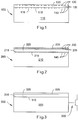
- FIG. 1 is a cross-sectional view of a reference electrode 100 according to an illustrative embodiment of the invention.
- the reference electrode 100 includes a conducting substrate 110 having a first surface 115.
- An ionically insulating, hydrophobic layer 120 is provided adjacent to the conducting substrate 110 first surface 115.
- the ionically insulating, hydrophobic layer 120 has a plurality of non-selective ion exchange sites 130 that are on an outer surface of the ionically insulating, hydrophobic layer 120.
- the conducting substrate 110 can be any electrically conductive material capable of forming an image charge 140.
- the conducting substrate 110 can be, for example, any metal or semiconductor material, as desired, and can be any suitable size.
- the conducting substrate 110 can include a non-conducting substrate with a conducting layer provided thereon.
- the ionically insulating, hydrophobic layer 120 can be any ionically insulating, hydrophobic material.
- the ionically insulating, hydrophobic layer 120 is non-porous, non-reactive and non-hydrating.
- the ionically insulating, hydrophobic layer 120 of the illustrative embodiment can also be chemically inert, thermally stable, mechanically stable, readily processable using standard IC processing techniques (spin coating, ion milling, etc.,) provide a stable reference potential over a pH range of 1-14, provide low interference background ionic strength, and/or demonstrate low potential drift over time.
- the ionically insulating, hydrophobic layer 120 may be a polymer or an amorphous polymer.
- the ionically insulating, hydrophobic layer 120 can be polytetrafluoroethylene, amorphous polytetrafluoroethylene, polystyrene, polyethylene, polypropylene, polycarbonate, polymethyl methacrylate, parylene, or mixtures thereof.
- Illustrative examples of useful ionically insulating, hydrophobic layer 120 material includes Teflon AFTM from DuPont, FluoroPelTM from Cytronics, or any other suitable ionically insulating hydrophobic layer material or material composition.
- the ionically insulating, hydrophobic layer 120 can have any thickness, however, it is preferable that the ionically insulating, hydrophobic layer 120 be as thin as possible, preferably less than or equal to 1 micron, but this is not required in all embodiments. In some embodiments, the ionically insulating, hydrophobic layer 120 has a thickness of 0.1 micron to 10 micron, 0.1 micron to 5 micron, or 0.5 micron to 1 micron.
- the plurality of non-selective ion exchange sites 130 can be formed from simple impurities on the ionically insulating, hydrophobic layer 120 surface. Alternatively, or in addition, the plurality of non-selective ion exchange sites 130 may include zeolyte particles.
- the non-selective ion exchange sites 130 allow the intercalation of background ions (cations or anions) from a sample fluid.
- the non-selective ion exchange sites 130 strips the ions (such as cations) from their hydrated surroundings and establishes a surface charge 135, and thus an accompanying image charge 140 on the underlying conductive substrate 110.
- the image charge represents the reference potential on the conductive substrate 210.
- background ion concentrations can be many orders of magnitude greater than analyte concentrations.
- a usable reference potential results when a non-selective ion exchange site 130 is used on the hydrophobic layer 120.
- a useful non-selective ion exchange site 130 particle is a zeolyte.
- Zeolyte particles can be disposed on the hydrophobic layer 120 in any useful amount to create a desired ion exchange site density.
- Useful zeolyte particles have a pore size that is greater than or equal to the size of an ammonium ion. Examples of commercial zeolytes from Zeolyte, International (Valley Forge, PA) are available under the tradenames; CBV5524, CP814E, CP814N and simple alumina (Al 2 Si 2 O 7 ).
- An adhesion promoter 116 can be disposed between the conductive substrate 110 and the ionically insulating, hydrophobic layer 120, but this is not required in all embodiments.
- the adhesion promoter 116 can be any material that helps join the ionically insulating, hydrophobic layer 120 to the remaining reference electrode 100.
- the adhesion promoter 116 can be a siloxane such as, for example, hexamethyl disiloxane, and the like.
- FIG. 2 is a cross-sectional view of a reference electrode 200 according to another illustrative embodiment of the present invention.
- the reference electrode 200 includes a conducting substrate 210 having a first surface 215.
- An ionically insulating, hydrophobic layer 220 is provided adjacent to the conducting substrate 210 first surface 215.
- a non-selective ion exchange layer 225 is disposed on the ionically insulating, hydrophobic layer 220.
- the conducting substrate 210 and the hydrophobic layer 220 can be similar to that described above.
- the non-selective ion exchange layer 225 includes non-selective ion exchange sites sufficient in quantity to achieve a desired ion exchange site density.
- the non-selective ion exchange sites are provided by non-selective ion exchange particles that are provided in sufficient density to constitute a layer 225, and may be formed with zeolyte particles.
- an adhesion promoter 216 can be disposed between the conductive substrate 210 and the ionically insulating, hydrophobic layer 220 as described above.
- the non-selective ion exchange sites 230 allow the intercalation of background ions (cations or anions) from the sample fluid.
- the non-selective ion exchange sites 230 strip the ions (such as cations) from their hydrated surroundings and establishes a surface charge 235 on the non-selective ion exchange layer 225, when then produces an accompanying image charge 240 on or in the underlying conductive substrate 210.
- the image charge produces the reference potential on or in the conductive substrate 210.
- Figure 3 is a cross-sectional view of a reference electrode 300 that is coupled to the gate of a Field Effect Transistor (FET).
- the reference electrode 300 of Figure 3 may be similar to the reference electrode 200 of Figure 2 .
- the conductive substrate 310 of the reference electrode 300 is electrically coupled to the gate of a FET device 350, as shown. While a FET device 350 is shown, it is contemplated that the conductive substrate 310 may be electrically coupled to any suitable electrical device or circuit, as desired.
- the conductive substrate 310 is preferably electrically coupled to a relatively high impendence input of an electrical device or circuit.
- FIG. 4 is a cross-sectional view of a reference electrode 400 according to yet another illustrative embodiment of the present invention.
- the reference electrode 400 includes a conducting substrate 410, with an ionically insulating, hydrophobic layer 420 positioned adjacent to the conducting substrate 410.
- a non-selective ion exchange layer 425 is shown disposed on the ionically insulating, hydrophobic layer 420.
- the conducting substrate 410 is disposed on a dielectric layer 460.
- the dielectric layer 460 is shown disposed on an integrated circuit substrate 480 that includes electronics 450 previously formed therein.
- the electronics 450 may include one or more conductive interconnect pads that are adapted to electrically interconnect to the conducting substrate 410 of the reference electrode 400.
- a VIA 470 is formed through the dielectric layer 460 to electrically connect the conductive substrate 410 and the one or more conductive interconnect pads of electronics 450.
- the electronics may be used to process the reference potential provided by the conducting substrate 410, preferably in conjunction with one or more electrical signals provided by one or more electrochemical sensors disposed in the test solution.
- FIG. 5 is a cross-sectional view of a reference electrode 500 according to yet another illustrative embodiment of the present invention.
- the reference electrode 500 includes a conducting substrate 510.
- the conducting substrate 510 is a semiconductor wafer.
- An ionically insulating, hydrophobic layer 520 is added adjacent to the conducting substrate 510 first surface 515.
- a non-selective ion exchange layer 525 is disposed on the ionically insulating, hydrophobic layer 520, as described above.
- the ionically insulating, hydrophobic layer 520 and the non-selective ion exchange layer 525 are provided on the back side of the semiconductor wafer.
- Electronics 550 may be fabricated into the front side of the semiconductor wafer, as shown.
- electronics 550 include a FET device.
- the substrate of the FET device 550 corresponds to the conducting substrate 510 of the reference electrode 500.
- the reference potential on the conducting substrate 510 is provided to the substrate of the FET device 550.
- the gate of the FET device 550 may be connected to the output of an electrochemical sensor that is in the test solution.
- the reference potential then may help offset or regulate the current supplied by the FET device 550 for a given gate voltage provided by the electrochemical sensor.
- Such a configuration may help provide a good chemical to electrical transducer.
- test fixture was a pH sensor and was designed and fabricated as described below.
- Parylene poly-p-xylene
- Parylene samples (“C” and “H”) were obtained from Specialty Coating Systems, Inc., (Clear Lake, WI), who specialize in vacuum deposition of parylene and other conformal coatings.
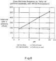
- Samples of Parylene "C”, a standard commercial grade material and Parylene "H”, a higher density material with lower water absorption were obtained as 0.5 ⁇ m pinhole free films on 3" silicone wafers (HTC supplied wafers). The films were tested in the test apparatus described in Part I, and the results are seen in Figure 6 .
- Teflon AF poly-tetrafluroethylene
- Samples of Teflon AF (1601S) were obtained from: DuPont Fluoproducts (Wilmington, DE). The material was received as a 6% w/w solution in FC-75 (a perfluronated hydrocarbon solvent from 3M). Wafers with native oxide were then spin-coated at 3000 RPMs for 30-40 seconds to get a 0.5 to 1 micron coating. After coating, the wafers were baked at 160°C for at least 10 minutes to boil off excess solvent and cure the polymer film. Elipsometry of the films indicated an average thickness of approximately 0.6 ⁇ m with an index of refraction of 12.3, which is consistent with the manufacturer's specifications. These films could be peeled from the substrate by rubbing a finger across them, and completely lifted off immediately on contact with our test buffers. Therefore, several methods of surface preparation were tried.
- HMDS hexamehtyl disiloxane
- the Telfon AF material shows a very good reference response.
- Typical results for Teflon AF with only bead blasting as a surface pretreatment is seen in Figure 7 .
- the initial response of the material is very good, being very linear and almost Nernstian.
- Our glass electrode was measured to be Nernstian versus a standard Ag/AgCI double junction reference.
- silicon alone shows an almost flat response, indicative of the fact that it is responding to pH in the same manner that the glass electrode did.
- these films show distinctly sub-Nernstian and non-linear behavior even when freshly made. After a few hours, the response slowly degrades towards a "silicon-like" behavior. This behavior is consistent with the nature of alumina and silicates that freely exchange protons.
- the embedded material does strongly affect the behavior of the film. This implies that zeolyte selection can tailor film characteristics.
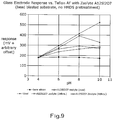
- CBV5524G (lot number 1822-18) and CP814E (lot number 1822-35) are size exclusion zeolytes with an internal cavity to accommodate large ammonium ions. Smaller ions all freely exchange with the cavity with no preference toward chemical nature. This is almost the ideal case for a reference electrode where "ion non-specificity" may be important.
- Figure 10 shows the typical result for CP814E (lot number 1822-35). Again, like Teflon AF alone, the response is very linear, although slightly super-Nernstian.
- Zeolyte CBV5524G (lot number 1822-18) has somewhat smaller pore size than CP814E (lot number 1822-35).
- its response is more understandably sub-Nernstian, having some small ion-and proton-exchange favoritism owing to its smaller pore size.
- Both materials are very stable over time (21 days) so long as material adhesion is maintained. Both materials significantly may enhance the speed of response of the film over native Teflon and permit smaller feature sizes as a result of a greatly increased ion-exchange site density.
Landscapes
- Chemical & Material Sciences (AREA)
- Life Sciences & Earth Sciences (AREA)
- Health & Medical Sciences (AREA)
- Physics & Mathematics (AREA)
- Chemical Kinetics & Catalysis (AREA)
- Electrochemistry (AREA)
- Molecular Biology (AREA)
- Analytical Chemistry (AREA)
- Biochemistry (AREA)
- General Health & Medical Sciences (AREA)
- General Physics & Mathematics (AREA)
- Immunology (AREA)
- Pathology (AREA)
- Investigating Or Analyzing Materials By The Use Of Electric Means (AREA)
Applications Claiming Priority (2)
| Application Number | Priority Date | Filing Date | Title |
|---|---|---|---|
| US10/681,440 US7318887B2 (en) | 2003-10-08 | 2003-10-08 | Solid state reference electrode |
| PCT/US2004/033016 WO2005036155A1 (en) | 2003-10-08 | 2004-10-08 | Solid state reference electrode |
Publications (2)
| Publication Number | Publication Date |
|---|---|
| EP1673617A1 EP1673617A1 (en) | 2006-06-28 |
| EP1673617B1 true EP1673617B1 (en) | 2018-04-11 |
Family
ID=34422282
Family Applications (1)
| Application Number | Title | Priority Date | Filing Date |
|---|---|---|---|
| EP04794389.9A Expired - Lifetime EP1673617B1 (en) | 2003-10-08 | 2004-10-08 | Solid state reference electrode |
Country Status (4)
| Country | Link |
|---|---|
| US (1) | US7318887B2 (enExample) |
| EP (1) | EP1673617B1 (enExample) |
| JP (1) | JP2007508547A (enExample) |
| WO (1) | WO2005036155A1 (enExample) |
Cited By (1)
| Publication number | Priority date | Publication date | Assignee | Title |
|---|---|---|---|---|
| US11873246B2 (en) | 2021-04-09 | 2024-01-16 | National Research Council Of Canada | Glass-containing pseudo-reference electrode for use in ion-selective electrode sensors and ion selective field-effect transistors |
Families Citing this family (4)
| Publication number | Priority date | Publication date | Assignee | Title |
|---|---|---|---|---|
| US20070045128A1 (en) * | 2005-08-19 | 2007-03-01 | Honeywell International Inc. | Chlorine dioxide sensor |
| EP2469275B1 (en) | 2010-12-24 | 2015-12-23 | Honeywell Romania S.R.L. | Cantilevered carbon dioxide sensor |
| ES3037403T3 (en) | 2018-09-21 | 2025-10-01 | Teralytic Holdings Inc | Extensible, multimodal sensor fusion platform for remote, proximal soil sensing |
| WO2021081424A1 (en) * | 2019-10-25 | 2021-04-29 | University Of Utah Research Foundation | Micro-balance biosensors to detect whole viruses |
Family Cites Families (11)
| Publication number | Priority date | Publication date | Assignee | Title |
|---|---|---|---|---|
| US3926764A (en) | 1971-05-19 | 1975-12-16 | Radiometer As | Electrode for potentiometric measurements |
| JPS5825221B2 (ja) | 1977-12-12 | 1983-05-26 | 株式会社クラレ | Fet比較電極 |
| CA1228895A (en) | 1984-01-19 | 1987-11-03 | Imants R. Lauks | Ambient sensing devices |
| JPS60163419A (ja) * | 1984-02-06 | 1985-08-26 | 東レ株式会社 | コンデンサ−用蒸着積層フイルム |
| IT1229691B (it) * | 1989-04-21 | 1991-09-06 | Eniricerche Spa | Sensore con antigene legato chimicamente a un dispositivo semiconduttore. |
| US5271820A (en) | 1992-06-19 | 1993-12-21 | Monsanto Company | Solid state pH sensor |
| NO951705D0 (no) | 1995-05-03 | 1995-05-03 | Sinvent As | All-solid state reference electrode |
| US6094335A (en) * | 1998-10-09 | 2000-07-25 | Advanced Micro Devices, Inc. | Vertical parallel plate capacitor |
| US6426861B1 (en) * | 1999-06-22 | 2002-07-30 | Lithium Power Technologies, Inc. | High energy density metallized film capacitors and methods of manufacture thereof |
| US6483694B1 (en) * | 1999-06-22 | 2002-11-19 | Showa Denko Kabushiki Kaisha | Electrode for electrolytic capacitor, electrolytic capacitor, and manufacturing method therefor |
| US6793789B2 (en) | 2000-09-30 | 2004-09-21 | Geun Sig Cha | Reference electrode with a polymeric reference electrode membrane |
-
2003
- 2003-10-08 US US10/681,440 patent/US7318887B2/en active Active
-
2004
- 2004-10-08 EP EP04794389.9A patent/EP1673617B1/en not_active Expired - Lifetime
- 2004-10-08 WO PCT/US2004/033016 patent/WO2005036155A1/en not_active Ceased
- 2004-10-08 JP JP2006534316A patent/JP2007508547A/ja not_active Ceased
Non-Patent Citations (3)
| Title |
|---|
| A WALCARIUS: "Zeolite-modi ed electrodes in electroanalytical chemistry", ANALYTICA CHIMICA ACTA, vol. 384, 22 March 1999 (1999-03-22), pages 1 - 16, XP055259296 * |
| MATYSIK SILKE ET AL: "A disposable electrode based on zeolite-polymer membranes for potentiometric titrations of ionic surfactants", 20 June 2002, SENSORS AND ACTUATORS B: CHEMICAL: INTERNATIONAL JOURNAL DEVOTED TO RESEARCH AND DEVELOPMENT OF PHYSICAL AND CHEMICAL TRANSDUCERS, ELSEVIER S.A, CH, PAGE(S) 104 - 108, ISSN: 0925-4005, XP002271483 * |
| MCDONALD J C ET AL: "Fabrication of microfluidic systems in poly(dimethylsiloxane)", ELECTROPHORESIS, WILEY INTERSCIENCE, DE, vol. 21, no. 1, 1 January 2000 (2000-01-01), pages 27 - 40, XP002278130, ISSN: 0173-0835, DOI: 10.1002/(SICI)1522-2683(20000101)21:1<27::AID-ELPS27>3.0.CO;2-C * |
Cited By (1)
| Publication number | Priority date | Publication date | Assignee | Title |
|---|---|---|---|---|
| US11873246B2 (en) | 2021-04-09 | 2024-01-16 | National Research Council Of Canada | Glass-containing pseudo-reference electrode for use in ion-selective electrode sensors and ion selective field-effect transistors |
Also Published As
| Publication number | Publication date |
|---|---|
| JP2007508547A (ja) | 2007-04-05 |
| WO2005036155A1 (en) | 2005-04-21 |
| EP1673617A1 (en) | 2006-06-28 |
| US20050077179A1 (en) | 2005-04-14 |
| US7318887B2 (en) | 2008-01-15 |
Similar Documents
| Publication | Publication Date | Title |
|---|---|---|
| US3905889A (en) | Miniature multifunctional electrochemical sensor for simultaneous carbon dioxide-pH measurements | |
| JP3588146B2 (ja) | イオン選択性センサおよびその形成方法 | |
| JPH0633063U (ja) | 黒鉛をベースとする固態ポリマー膜イオン選択性電極 | |
| US7179354B2 (en) | Electrochemical sensor | |
| CA2150017C (en) | Reference electrode | |
| US20190120787A1 (en) | Graphene-based sensor and method of fabricating same | |
| EP1673617B1 (en) | Solid state reference electrode | |
| JPH06508432A (ja) | 液体の電気的分析とそれに使用する検出素子 | |
| Kwon et al. | An all-solid-state reference electrode based on the layer-by-layer polymer coating | |
| Herlem et al. | pH sensing at Pt electrode surfaces coated with linear polyethylenimine from anodic polymerization of ethylenediamine | |
| Zine et al. | Hydrogen-selective microelectrodes based on silicon needles | |
| Wróblewski et al. | Towards advanced chemical microsensors—an overview | |
| JP2003207476A (ja) | イオンセンサ及びそれを用いた生化学自動分析装置 | |
| Yamada et al. | All‐solid‐state Fluoride Ion‐selective Electrode using LaF3 Single Crystal with Poly (3, 4‐ethylenedioxythiophene) as Solid Contact Layer | |
| US3975681A (en) | Electrode for measuring thickness of dielectric layers on conductive substrates | |
| Kalidoss et al. | Solid-state planar reference electrode with ion-selective electrodes for clinical diagnosis | |
| Sun et al. | A miniaturized seven-electrode conductivity and temperature integrated sensor | |
| Spelthahn et al. | Development of a thin‐film sensor array for analytical monitoring of heavy metals in aqueous solutions | |
| Winkler et al. | Ac voltammetric measurements of fast charge-transfer processes at ultramicroelectrodes | |
| Iken et al. | Development of a Combined pH‐and Redox‐Sensitive Bi‐Electrode Glass Thin‐Film Sensor | |
| WO2021229222A1 (en) | Electrochemical sensing | |
| US6019880A (en) | HgO-modified electrode for anodic stripping analysis | |
| Figueroa et al. | Two-liquid wetting and phase electrowetting as a probe for surface chemistry of hydrophobic materials | |
| Migdalski et al. | A miniaturized and integrated galvanic cell for the potentiometric measurement of ions in biological liquids | |
| Bae et al. | Research on an Electrochemical Salinity Sensor with Indium-Tin-Oxide Conductive Ceramic Electrodes |
Legal Events
| Date | Code | Title | Description |
|---|---|---|---|
| PUAI | Public reference made under article 153(3) epc to a published international application that has entered the european phase |
Free format text: ORIGINAL CODE: 0009012 |
|
| 17P | Request for examination filed |
Effective date: 20060125 |
|
| AK | Designated contracting states |
Kind code of ref document: A1 Designated state(s): DE FR GB SE |
|
| DAX | Request for extension of the european patent (deleted) | ||
| RBV | Designated contracting states (corrected) |
Designated state(s): DE FR GB SE |
|
| 17Q | First examination report despatched |
Effective date: 20090316 |
|
| RAP1 | Party data changed (applicant data changed or rights of an application transferred) |
Owner name: RHODES, MICHAEL L. Owner name: HONEYWELL INTERNATIONAL INC. |
|
| GRAJ | Information related to disapproval of communication of intention to grant by the applicant or resumption of examination proceedings by the epo deleted |
Free format text: ORIGINAL CODE: EPIDOSDIGR1 |
|
| GRAP | Despatch of communication of intention to grant a patent |
Free format text: ORIGINAL CODE: EPIDOSNIGR1 |
|
| GRAP | Despatch of communication of intention to grant a patent |
Free format text: ORIGINAL CODE: EPIDOSNIGR1 |
|
| INTG | Intention to grant announced |
Effective date: 20171201 |
|
| GRAS | Grant fee paid |
Free format text: ORIGINAL CODE: EPIDOSNIGR3 |
|
| GRAA | (expected) grant |
Free format text: ORIGINAL CODE: 0009210 |
|
| AK | Designated contracting states |
Kind code of ref document: B1 Designated state(s): DE FR GB SE |
|
| REG | Reference to a national code |
Ref country code: GB Ref legal event code: FG4D |
|
| REG | Reference to a national code |
Ref country code: DE Ref legal event code: R096 Ref document number: 602004052587 Country of ref document: DE |
|
| REG | Reference to a national code |
Ref country code: SE Ref legal event code: TRGR |
|
| REG | Reference to a national code |
Ref country code: DE Ref legal event code: R097 Ref document number: 602004052587 Country of ref document: DE |
|
| PLBE | No opposition filed within time limit |
Free format text: ORIGINAL CODE: 0009261 |
|
| STAA | Information on the status of an ep patent application or granted ep patent |
Free format text: STATUS: NO OPPOSITION FILED WITHIN TIME LIMIT |
|
| 26N | No opposition filed |
Effective date: 20190114 |
|
| REG | Reference to a national code |
Ref country code: DE Ref legal event code: R119 Ref document number: 602004052587 Country of ref document: DE |
|
| REG | Reference to a national code |
Ref country code: SE Ref legal event code: EUG |
|
| GBPC | Gb: european patent ceased through non-payment of renewal fee |
Effective date: 20181008 |
|
| PG25 | Lapsed in a contracting state [announced via postgrant information from national office to epo] |
Ref country code: DE Free format text: LAPSE BECAUSE OF NON-PAYMENT OF DUE FEES Effective date: 20190501 Ref country code: SE Free format text: LAPSE BECAUSE OF NON-PAYMENT OF DUE FEES Effective date: 20181009 |
|
| PG25 | Lapsed in a contracting state [announced via postgrant information from national office to epo] |
Ref country code: FR Free format text: LAPSE BECAUSE OF NON-PAYMENT OF DUE FEES Effective date: 20181031 |
|
| PG25 | Lapsed in a contracting state [announced via postgrant information from national office to epo] |
Ref country code: GB Free format text: LAPSE BECAUSE OF NON-PAYMENT OF DUE FEES Effective date: 20181008 |