EP1672758A2 - Semiconductor lasers - Google Patents
Semiconductor lasers Download PDFInfo
- Publication number
- EP1672758A2 EP1672758A2 EP05112234A EP05112234A EP1672758A2 EP 1672758 A2 EP1672758 A2 EP 1672758A2 EP 05112234 A EP05112234 A EP 05112234A EP 05112234 A EP05112234 A EP 05112234A EP 1672758 A2 EP1672758 A2 EP 1672758A2
- Authority
- EP
- European Patent Office
- Prior art keywords
- lasers
- laser
- semiconductor
- structures
- current flow
- Prior art date
- Legal status (The legal status is an assumption and is not a legal conclusion. Google has not performed a legal analysis and makes no representation as to the accuracy of the status listed.)
- Granted
Links
- 239000004065 semiconductor Substances 0.000 title claims abstract description 91
- 239000000463 material Substances 0.000 claims abstract description 37
- 238000000034 method Methods 0.000 claims description 52
- 230000004044 response Effects 0.000 claims description 9
- 230000000638 stimulation Effects 0.000 claims description 7
- 229910052751 metal Inorganic materials 0.000 description 50
- 239000002184 metal Substances 0.000 description 50
- 230000009977 dual effect Effects 0.000 description 27
- 238000001228 spectrum Methods 0.000 description 21
- 230000003287 optical effect Effects 0.000 description 20
- 239000000758 substrate Substances 0.000 description 17
- 239000004020 conductor Substances 0.000 description 14
- 230000008569 process Effects 0.000 description 8
- 238000013459 approach Methods 0.000 description 7
- 230000012447 hatching Effects 0.000 description 7
- 239000000243 solution Substances 0.000 description 7
- 238000005253 cladding Methods 0.000 description 6
- 238000009826 distribution Methods 0.000 description 6
- JBRZTFJDHDCESZ-UHFFFAOYSA-N AsGa Chemical compound [As]#[Ga] JBRZTFJDHDCESZ-UHFFFAOYSA-N 0.000 description 5
- 230000008859 change Effects 0.000 description 5
- 230000001427 coherent effect Effects 0.000 description 5
- 230000003993 interaction Effects 0.000 description 5
- 238000000608 laser ablation Methods 0.000 description 5
- 238000000059 patterning Methods 0.000 description 5
- 238000007747 plating Methods 0.000 description 5
- 229910001218 Gallium arsenide Inorganic materials 0.000 description 4
- 238000000151 deposition Methods 0.000 description 4
- 239000011810 insulating material Substances 0.000 description 4
- 150000002500 ions Chemical class 0.000 description 4
- 238000002955 isolation Methods 0.000 description 4
- 238000004519 manufacturing process Methods 0.000 description 4
- 230000004048 modification Effects 0.000 description 4
- 238000012986 modification Methods 0.000 description 4
- 238000004088 simulation Methods 0.000 description 4
- 238000012546 transfer Methods 0.000 description 4
- 229910021417 amorphous silicon Inorganic materials 0.000 description 3
- 238000003491 array Methods 0.000 description 3
- 230000008021 deposition Effects 0.000 description 3
- 238000000866 electrolytic etching Methods 0.000 description 3
- 238000009713 electroplating Methods 0.000 description 3
- 238000005530 etching Methods 0.000 description 3
- 238000010438 heat treatment Methods 0.000 description 3
- 150000004767 nitrides Chemical class 0.000 description 3
- 238000012360 testing method Methods 0.000 description 3
- 230000009471 action Effects 0.000 description 2
- 230000008901 benefit Effects 0.000 description 2
- 238000007796 conventional method Methods 0.000 description 2
- 238000013461 design Methods 0.000 description 2
- 230000000694 effects Effects 0.000 description 2
- 239000007772 electrode material Substances 0.000 description 2
- 238000004070 electrodeposition Methods 0.000 description 2
- 239000012634 fragment Substances 0.000 description 2
- 230000014509 gene expression Effects 0.000 description 2
- AMGQUBHHOARCQH-UHFFFAOYSA-N indium;oxotin Chemical compound [In].[Sn]=O AMGQUBHHOARCQH-UHFFFAOYSA-N 0.000 description 2
- 238000002347 injection Methods 0.000 description 2
- 239000007924 injection Substances 0.000 description 2
- 150000002739 metals Chemical class 0.000 description 2
- 238000000623 plasma-assisted chemical vapour deposition Methods 0.000 description 2
- 230000007480 spreading Effects 0.000 description 2
- 238000003892 spreading Methods 0.000 description 2
- 229910002601 GaN Inorganic materials 0.000 description 1
- JMASRVWKEDWRBT-UHFFFAOYSA-N Gallium nitride Chemical compound [Ga]#N JMASRVWKEDWRBT-UHFFFAOYSA-N 0.000 description 1
- UFHFLCQGNIYNRP-UHFFFAOYSA-N Hydrogen Chemical compound [H][H] UFHFLCQGNIYNRP-UHFFFAOYSA-N 0.000 description 1
- 239000011149 active material Substances 0.000 description 1
- 229910045601 alloy Inorganic materials 0.000 description 1
- 239000000956 alloy Substances 0.000 description 1
- 238000004458 analytical method Methods 0.000 description 1
- QVGXLLKOCUKJST-UHFFFAOYSA-N atomic oxygen Chemical compound [O] QVGXLLKOCUKJST-UHFFFAOYSA-N 0.000 description 1
- 239000006059 cover glass Substances 0.000 description 1
- 239000013078 crystal Substances 0.000 description 1
- 230000007547 defect Effects 0.000 description 1
- 230000001627 detrimental effect Effects 0.000 description 1
- 238000007772 electroless plating Methods 0.000 description 1
- 230000005670 electromagnetic radiation Effects 0.000 description 1
- 230000008020 evaporation Effects 0.000 description 1
- 238000001704 evaporation Methods 0.000 description 1
- 239000001257 hydrogen Substances 0.000 description 1
- 229910052739 hydrogen Inorganic materials 0.000 description 1
- -1 hydrogen or oxygen Chemical class 0.000 description 1
- 239000007943 implant Substances 0.000 description 1
- 239000012535 impurity Substances 0.000 description 1
- 239000012212 insulator Substances 0.000 description 1
- 238000005468 ion implantation Methods 0.000 description 1
- 230000007246 mechanism Effects 0.000 description 1
- 229910044991 metal oxide Inorganic materials 0.000 description 1
- 150000004706 metal oxides Chemical class 0.000 description 1
- ORQBXQOJMQIAOY-UHFFFAOYSA-N nobelium Chemical compound [No] ORQBXQOJMQIAOY-UHFFFAOYSA-N 0.000 description 1
- 239000001301 oxygen Substances 0.000 description 1
- 229910052760 oxygen Inorganic materials 0.000 description 1
- 230000000737 periodic effect Effects 0.000 description 1
- 238000000206 photolithography Methods 0.000 description 1
- 238000005498 polishing Methods 0.000 description 1
- 230000006798 recombination Effects 0.000 description 1
- 238000005215 recombination Methods 0.000 description 1
- 230000009467 reduction Effects 0.000 description 1
- 238000002310 reflectometry Methods 0.000 description 1
- 239000000523 sample Substances 0.000 description 1
- 230000035945 sensitivity Effects 0.000 description 1
- 229910000679 solder Inorganic materials 0.000 description 1
- 230000003595 spectral effect Effects 0.000 description 1
- 238000004528 spin coating Methods 0.000 description 1
- 238000004544 sputter deposition Methods 0.000 description 1
- 230000001052 transient effect Effects 0.000 description 1
- 230000007704 transition Effects 0.000 description 1
Images


Classifications
-
- H—ELECTRICITY
- H01—ELECTRIC ELEMENTS
- H01S—DEVICES USING THE PROCESS OF LIGHT AMPLIFICATION BY STIMULATED EMISSION OF RADIATION [LASER] TO AMPLIFY OR GENERATE LIGHT; DEVICES USING STIMULATED EMISSION OF ELECTROMAGNETIC RADIATION IN WAVE RANGES OTHER THAN OPTICAL
- H01S5/00—Semiconductor lasers
- H01S5/04—Processes or apparatus for excitation, e.g. pumping, e.g. by electron beams
- H01S5/042—Electrical excitation ; Circuits therefor
- H01S5/0425—Electrodes, e.g. characterised by the structure
- H01S5/04256—Electrodes, e.g. characterised by the structure characterised by the configuration
-
- H—ELECTRICITY
- H01—ELECTRIC ELEMENTS
- H01S—DEVICES USING THE PROCESS OF LIGHT AMPLIFICATION BY STIMULATED EMISSION OF RADIATION [LASER] TO AMPLIFY OR GENERATE LIGHT; DEVICES USING STIMULATED EMISSION OF ELECTROMAGNETIC RADIATION IN WAVE RANGES OTHER THAN OPTICAL
- H01S5/00—Semiconductor lasers
- H01S5/40—Arrangement of two or more semiconductor lasers, not provided for in groups H01S5/02 - H01S5/30
- H01S5/4025—Array arrangements, e.g. constituted by discrete laser diodes or laser bar
- H01S5/4031—Edge-emitting structures
-
- H—ELECTRICITY
- H01—ELECTRIC ELEMENTS
- H01S—DEVICES USING THE PROCESS OF LIGHT AMPLIFICATION BY STIMULATED EMISSION OF RADIATION [LASER] TO AMPLIFY OR GENERATE LIGHT; DEVICES USING STIMULATED EMISSION OF ELECTROMAGNETIC RADIATION IN WAVE RANGES OTHER THAN OPTICAL
- H01S5/00—Semiconductor lasers
- H01S5/02—Structural details or components not essential to laser action
- H01S5/024—Arrangements for thermal management
- H01S5/02469—Passive cooling, e.g. where heat is removed by the housing as a whole or by a heat pipe without any active cooling element like a TEC
-
- H—ELECTRICITY
- H01—ELECTRIC ELEMENTS
- H01S—DEVICES USING THE PROCESS OF LIGHT AMPLIFICATION BY STIMULATED EMISSION OF RADIATION [LASER] TO AMPLIFY OR GENERATE LIGHT; DEVICES USING STIMULATED EMISSION OF ELECTROMAGNETIC RADIATION IN WAVE RANGES OTHER THAN OPTICAL
- H01S5/00—Semiconductor lasers
- H01S5/04—Processes or apparatus for excitation, e.g. pumping, e.g. by electron beams
- H01S5/042—Electrical excitation ; Circuits therefor
- H01S5/0425—Electrodes, e.g. characterised by the structure
- H01S5/04254—Electrodes, e.g. characterised by the structure characterised by the shape
-
- H—ELECTRICITY
- H01—ELECTRIC ELEMENTS
- H01S—DEVICES USING THE PROCESS OF LIGHT AMPLIFICATION BY STIMULATED EMISSION OF RADIATION [LASER] TO AMPLIFY OR GENERATE LIGHT; DEVICES USING STIMULATED EMISSION OF ELECTROMAGNETIC RADIATION IN WAVE RANGES OTHER THAN OPTICAL
- H01S5/00—Semiconductor lasers
- H01S5/40—Arrangement of two or more semiconductor lasers, not provided for in groups H01S5/02 - H01S5/30
- H01S5/4025—Array arrangements, e.g. constituted by discrete laser diodes or laser bar
- H01S5/4087—Array arrangements, e.g. constituted by discrete laser diodes or laser bar emitting more than one wavelength
Abstract
Description
- The present invention relates generally to techniques for semiconductor lasers. For example, the invention relates to techniques in which two or more beams of coherent light are emitted, such as from different active regions of a laser structure.
- Various techniques have been proposed for multiple lasers or multi-beam lasers, and many such techniques are concerned with optical, electrical, and thermal interactions. U.S. Patent No. 6,052,399, for example, describes an independently addressable laser array in which a high density, edge emitting laser array structure has native oxide layers formed in adjacent grooves in a p-cladding layer; the native oxide layers provide optical confinement and electrical isolation. U.S. Patent No. 5,513,200 similarly describes a monolithic array of independently addressable diode lasers that are closely spaced but have low thermal, electrical, and optical crosstalk; an isolation groove is formed between adjacent laser elements, which are defined by rib loaded waveguides created by etching mesas above a planar active multilayer waveguide. U.S. Patent No. 6,744,800 describes nitride based laser diode arrays on an insulating substrate, with contact layouts that reduce electrical and thermal crosstalk between laser diodes; buried layers are used to provide compact and low crosstalk contact structures. U.S. Patent Nos. 4,870,652 and 4,980,893 both describe monolithic high density arrays of independently addressable semiconductor laser sources in which laser emitters or elements can be in close center-to-center proximity, e.g. on 3-10 µm centers, without undesirable phase locking and with minimal electrical and thermal interaction or crosstalk between independently addressed lasing elements.
- Previous techniques, however, are limited in the ways they deal with optical interactions. It would be advantageous to have additional techniques for semiconductor laser structures, and, more specifically, it would be advantageous to have additional techniques that can be applied to alleviate optical interaction problems.
- The invention provides various exemplary embodiments of devices, apparatus, and methods. In general, each embodiment involves a laser or laser structure in which at least two semiconductor structures emit light. The semiconductor structures may be substantially identical or may include the same semiconductor material and have substantially the same geometry.
- In one embodiment of the device as defined in
claim 1, each laser's current flow structure includes a metal contact layer. - In a further embodiment the differently structured current flow structures affect phase locking between the pair of lasers.
- In a further embodiment the differently structured current flow structures cause the pair of lasers to have different threshold currents.
- In a further embodiment the differently structured current flow structures cause the pair of lasers to have different operating temperatures.
- In a further embodiment the pair of lasers are independently addressable.
- In a further embodiment the device further comprises: a laser structure on the support structure, the laser structure including: the semiconductor structures of the lasers in the subset.
- In a further embodiment the semiconductor structures of the lasers in the subset include concurrently formed epitaxial material.
- In one embodiment of the apparatus as defined in claim 7 the apparatus is a printer.
- In a further embodiment the current flow structures of the pair of lasers are sufficiently different to prevent phase locking between the pair of lasers when each is driven within its respective range of operating conditions.
- In one embodiment of the device as defined in
claim 8 each laser's wavelength control structure includes a metal contact layer. - In one embodiment of the device as defined in claim 9, the contact structures of the first and second lasers include first and second patterned conductive layers, respectively; each conductive layer extending in the respective laser's longitudinal direction; the first laser's semiconductor structure having at least one isolated area in which it does not receive electrical current from a covering part of the first patterned conductive layer.
- In a further embodiment the second laser's semiconductor structure has at least one isolated area in which it does not receive electrical current from a covering part of the second patterned conductive layer; the semiconductor structures of the first and second lasers having different isolated areas so that the first and second lasers have different threshold currents.
- In a further embodiment each isolated area is an uncovered area in which the first laser's semiconductor structure is not covered by the first patterned conductive layer.
- In a further embodiment the contact structures of the first and second lasers include first and second patterned metal layers, respectively; the first patterned metal layer being thicker than the second patterned metal layer.
- In a further embodiment the contact structures of the first and second lasers include first and second plated layers, respectively; the first plated layer being differently plated than the second plated layer.
- In a further embodiment the contact structures of the first and second lasers have different lengths in the respective laser's longitudinal direction.
- In a further embodiment the contact structure of the first laser includes:
- a conductive layer; and
- a patterned layer with high electrical resistance between the semiconductor structure and the conductive layer in the contact structure; the patterned layer being different than the contact structure of the second laser.
- In a further embodiment the semiconductor structure of the first laser comprises:
- one or more regions of high electrical resistance adjacent the first laser's contact structure; the regions of high electrical resistance being different than in the second laser.
- In a further embodiment the regions of high electrical resistance are ion implanted regions.
- In one embodiment of the method as defined in
claim 10, the act of producing the semiconductor structures comprises: producing the semiconductor structures concurrently. - In a further embodiment the current flow structure of each of the pair of lasers includes a respective plated layer; the act of producing the current flow structures comprises: plating the respective plated layers of the pair of lasers differently.
- These and other features and advantages of exemplary embodiments of the invention are described below with reference to the accompanying drawings, in which like reference numerals refer to components that are alike or similar in structure or function.
-
- Fig. 1 is a schematic drawing of oscilloscope traces showing light power fluctuation caused by optical interference in a dual beam laser structure.
- Fig. 2 shows graphs illustrating a typical relationship between simplified spectra of non-phase locking dual beam lasers when operated one at a time and concurrently.
- Fig. 3 is a top plan view of a dual beam laser structure in which contact structures are structured differently to affect phase locking.
- Fig. 4 is a cross-sectional view taken along the line 4-4' in Fig. 3, with related circuitry shown schematically.
- Fig. 5 is a graph showing gain as a function of photon energy for the dual beam laser structure in Figs. 3 and 4.
- Fig. 6 is a top plan view of an alternative implementation of a dual beam laser in which contact structures are structured differently to affect phase locking.
- Fig. 7 shows graphs comparing light output as a function of current for a symmetric dual beam laser with that for the dual beam laser structure in Fig. 6.
- Fig. 8 shows graphs comparing intensity as a function of wavelength for the dual beam laser structure in Fig. 6, operated one at a time and concurrently.
- Figs. 9 and 10 are top plan views of other alternative implementations of a dual beam laser in which contact structures are structured differently to affect phase locking.
- Fig. 11 is a top plan view of a dual beam laser structure in which contact structures have different thicknesses to affect phase locking.
- Fig. 12 is a schematic, distorted cross-sectional view taken along the line 12-12' in Fig. 11.
- Fig. 13 is a graph showing temperature as a function of position in a simulation of the dual beam laser structure of Figs. 11 and 12.
- Fig. 14 is a top plan view of a stage in producing dual beam laser structures as in Figs. 11 and 12.
- Fig. 15 is a top plan view of a dual beam laser structure in which one laser's contact structure includes a patterned high resistance layer that is different than the other laser's contact structure.
- Fig. 16 is a cross-sectional view taken along the line 16-16' in Fig. 15.
- Fig. 17 is a partially cutaway top plan view of an implementation of a quad beam laser in which one laser's contact structure includes a patterned high resistance layer different than another laser's contact structure.
- Fig. 18 is a top plan view of a dual beam laser structure in which one laser's epitaxial semiconductor structure includes a high resistance region different than the other laser.
- Fig. 19 is a cross-sectional view taken along the line 19-19' in Fig. 18.
- In the following detailed description, numeric ranges are provided for various aspects of the implementations described. These recited ranges are to be treated as examples only, and are not intended to limit the scope of the claims. In addition, a number of materials are identified as suitable for various facets of the implementations. These recited materials are to be treated as exemplary, and are not intended to limit the scope of the claims.
- "Light" refers herein to electromagnetic radiation of any wavelength.
- The term "laser" is used herein to mean any region, element, component, or device in which transitions of atoms or molecules between energy levels can be stimulated to cause emission of coherent light, such as in the ultraviolet, visible, or infrared regions of the spectrum. A "laser structure" is any structure that includes one or more lasers.
- A "semiconductor structure" is any structure that includes sufficient semiconductor material to behave as a semiconductor, i.e. having electrical conductivity that can change between that of a conductor and that of an insulator depending on conditions such as temperature, presence of impurities, crystal defects, and so forth. A "semiconductor laser" is a laser in which a semiconductor structure emits light in response to stimulation.
- Various techniques have been developed for producing structures with one or more dimensions smaller than 1 mm. In particular, some techniques for producing such structures are referred to as "microfabrication." Examples of microfabrication include various techniques for depositing materials such as growth of epitaxial material, sputter deposition, evaporation techniques, plating techniques, spin coating, and other such techniques; techniques for patterning materials, such as photolithography; techniques for polishing, planarizing, or otherwise modifying exposed surfaces of materials; and so forth.
- In general, structures, elements, and components described herein are supported on a "support structure" or "support surface", which terms are used herein to mean a structure or a structure's surface that can support other structures; more specifically, a support structure could be a "substrate", used herein to mean a support structure on a surface of which other structures can be formed or attached by microfabrication or similar processes.
- The surface of a substrate or other support structure is treated herein as providing a directional orientation as follows: A direction away from the surface is "up" or "over", while a direction toward the surface is "down" or "under". The terms "upper" and "top" are typically applied to structures, components, or surfaces disposed away from the surface, while "lower" or "underlying" are applied to structures, components, or surfaces disposed toward the surface. In general, it should be understood that the above directional orientation is arbitrary and only for ease of description, and that a support structure or substrate may have any appropriate orientation.
- An "edge emitting laser" is a semiconductor laser on a support surface in which coherent light is emitted in a direction that is not perpendicular to the support surface, typically from an edge of a semiconductor structure. Within an edge emitting laser, the direction of light emission is referred to as the laser's "longitudinal direction".
- Fig. 1 is a schematic
drawing showing oscilloscope 10, the screen of which shows a trace of power output from a test apparatus as a function of time. In the test apparatus, dual beam infrared lasers were aimed at an aperture, producing an interference pattern on a photodetector behind the aperture. The lasers were activated with a periodic pulse signal provided concurrently to both lasers, and the output from the photodector was provided tooscilloscope 10. - The resulting trace shown in Fig. 1 includes two main parts, ON
trace 20 andOFF trace 22, corresponding respectively to the time during which the pulsed signal is high and the time during which it is low in each period. The trace in Fig. 1, however, shows additional lines and areas that indicate power fluctuations due to interference between the two lasers. For example,lines line 32, the output power stabilized at a value higher thanON trace 20.Area 34, on the other hand, illustrates variations in output power that began to occur after the lasers had been emitting for approximately half of the pulse width, at which time output power wandered away fromON trace 20 during many of the pulses.Lines area 34 are typical of trace features due to laser interference. But the underlying interference process is random and uncontrolled, so that many other types of features would indicate interference. If the lasers were emitting independently, without interference,oscilloscope 10 would show only ONtrace 20 andOFF trace 22. - Experimentation shows that power fluctuations as illustrated by
lines area 34 are likely due to coherent optical interference between two light beams from a dual beam laser device, such as when both laser emitters are turned on to obtain about the same output power. This type of power fluctuation can occur if the two lasers are emitting at the same wavelength and are phase-locked for sufficient periods of time during operation. - As used herein, the term "phase locking" refers to an interference phenomenon in which two or more sources of coherent light at the same wavelength interact so that their emitted light is in phase. Since there is no known mechanism by which unreflected emitted beams alone could cause phase locking, it is generally believed that phase locking depends on some sort of "cross talk," meaning a transfer of information between laser elements. Optical cross talk, for example, could transfer phase information from one laser element to another. Optical cross talk can be internal, such as by scattering within a device, or external, such as by reflection of an emitted beam of one laser to another.
- Phase locking is easily induced between closely spaced lasers that share identical active layers and have the same device structure. For such lasers, even a small amount of optical cross talk can produce phase locking if the two lasers are emitting at the same wavelength.
- In another typical case, lasers may emit at slightly different wavelengths, but their spectra of emission may overlap sufficiently under certain operating conditions to cause phase locking. As used herein, the term "operating conditions" refers to a combination of conditions under which the laser is operated, such as current, voltage, output power, temperature, and so forth. In an apparatus, such as a printer, a laser may operate within a "range of operating conditions", meaning all the combinations of operating conditions encountered in normal operation of the apparatus. Overlap between wavelength spectra under certain operating conditions allows phase locking in the presence of optical cross talk.
- Since the wavelength spectrum of an edge-emitting laser shifts with operating current due to thermally-induced bandgap shrinkage, changes in operating current can cause spectra of lasers to overlap. More specifically, higher operating currents produce more heating, causing material gain profile to shift to longer wavelengths. The lasing spectrum shifts correspondingly with the gain peak. For example, for most gallium arsenide (GaAs) lasers, the spectrum is red shifted by about 0.3 nm/degree Centigrade. As operating current of one laser element of a dual beam device changes, its spectrum may sweep across the spectrum of the other laser element, resulting in overlap. Similarly, two closely-spaced thermally-coupled lasers using the same active material and having identical device structures would have overlapping wavelength spectra under operating conditions in which their operating currents and output powers are approximately the same.
- Although phase locking might be desirable or useful in some contexts, it causes problems in others. For example, if a dual beam laser device susceptible to phase locking is used in a laser printer, some areas of an image will be incompletely printed due to incomplete toner transfer. This phenomenon, referred to as "hatching," typically occurs when dual beam lasers are used in
interlace 1 scan mode. In this case, phase locking and the resulting power fluctuations are detrimental to printer operation. - Because hatching is a serious problem in printers, dual beam lasers cannot be used in a given printer if they are susceptible to phase locking when operated in the printer's range of operating conditions. One approach is to simply test each laser device, in the manner described above in relation to Fig. 1 or in a similar manner, to determine whether hatching will occur. If a laser device would produce hatching, it must then be thrown away, resulting in a severe yield penalty and narrowly constraining how and in which printer platform each laser device can be used.
- One solution to phase locking and the resulting power fluctuations would be to eliminate optical cross talk, including scattering within the device structure itself, back reflection off of the cover glass of a package containing the device, and so forth. In a dual beam laser device, a quad beam laser device, or another multi-beam laser device, the laser elements are positioned in close proximity, making it difficult to block out all sources of optical cross talk. Furthermore, a minute internal or external perturbation could negate a reduction in internal cross talk.
- Fig. 2 illustrates another solution to the problem of phase locking due to optical cross talk. As illustrated in
boxes box 50, the central wavelength for laser A is λA; similarly the central wavelength for the spectrum of laser B is λB. The difference ΔλAB (=λB-λA) is sufficiently great that when both lasers A and B are turned on, their combined spectrum, shown inbox 54, includes two distinct peaks without overlap. This is true even though the peak attributable to each laser has illustratively shifted somewhat toward the other laser's wavelength. Since the two peaks do not overlap, phase locking is prevented even with small amounts of internal or external optical cross talk. As a result, power fluctuations of the type illustrated in Fig. 1 do not occur under operating conditions of interest, and hatching is also prevented if the dual beam device is used in a printer. - The general solution illustrated in Fig. 2 is inherently present where lasers A and B have different semiconductor structures and, therefore, different central wavelengths. See, for example, U.S. Patent No. 6, 136,623, describing multiple wavelength laser arrays fabricated by flip-chip bonding from laser structures on different substrates.
- The general solution illustrated in Fig. 2 is also applicable in other contexts, even under a constraint such as that lasers A and B must have substantially identical semiconductor structures or that their semiconductor structures must include the same semiconductor material and have substantially the same geometry. This type of constraint, referred to herein as a "semiconductor symmetry constraint," often applies to commercially available laser products. For example, Sony Corporation has a dual spot two-beam laser product designated SLD263KP in which two adjacent edge-emitting lasers are substantially identical, separated by a groove or trench within which sidewalls are passivated for greater isolation. It would be advantageous to implement the general solution of Fig. 2 for such a product without modifying the semiconductor structures of the lasers, especially if this could be done without modifying the fabrication process, the device architecture, or the epitaxial design.
- Even where two or more lasers satisfy a semiconductor symmetry constraint, other parts of the lasers can be differently structured, and some of these differences can result in different wavelength spectra. In a given application, the laser elements will be operated within a range of operating conditions, so that the difference in wavelength will be sufficient if it prevents phase locking within the relevant range of operating conditions. In other words, it is not necessary to prevent phase locking under all possible operating conditions, but only under those that will be encountered in actual operation. As used herein, the term "required difference in wavelength" refers to a difference between wavelengths emitted by two lasers that is sufficient to prevent interference between the lasers within the range of operating conditions of the application for which they are used.
- Fig. 3 shows dual
beam laser device 100, with independentlyaddressable laser elements Arrows 106 show wherelaser elements Arrows 106 are at the end ofrespective laser stripes laser stripe 112 in turn being completely covered bycontact metal 116 andlaser stripe 114 being partially covered bycontact metal 118. - Fig. 3 also shows a difference in structure between
contact metal 116 andcontact metal 118. Whilemetal pad 116 completely coverslaser stripe 112 along its entire length L,contact metal 118 does not cover a length of X at the emitting end oflaser stripe 114 and similarly does not coverlaser stripe 114 for a length of Y at the opposite end oflaser stripe 114. Therefore,device 100 illustrates differently structured current flow structures forlasers - Unless specified as electrical or thermal, the terms "current" and "current flow" are used herein to include electrical current or thermal current or other conductive transfer of electrical or thermal energy between positions or regions; in general, these terms include not only total current but also distribution of current in varying current densities. Accordingly, the term "conductive path" means any path along which one or both of electrical or thermal current can flow through a structure. Although most semiconductor lasers have a single structure that provides conductive paths for both electrical and thermal current to or from a semiconductor structure, a laser's current flow structure could include more than one such structure or even separate substructures for electrical and thermal currents.
- Fig. 4 is a cross-sectional view of Fig. 3 along the line 4-4'. The same cross-section would be seen through the region at the opposite end of
laser stripe 114, along a line parallel to line 4-4'. -
Substrate 120 hassurface 122 at whichdevice 100 has been fabricated.Substrate 120 can, for example, be an n-type GaAs substrate, in which case it is conductive and would be connected to a common ground as shown in Fig. 4. -
Epitaxial structure 130 for bothlasers surface 122 by epitaxial deposition, such as by conventional techniques described, for example, in U.S. Patent No. 6,052,399, incorporated herein by reference.Epitaxial structure 130 can include an n-type lower cladding layer, an undoped lower confinement layer, an active layer, an undoped upper confinement layer, and a p-type upper cladding layer.Laser stripes lasers lasers - In areas other than
laser stripes layer 132 is present, and can be, for example, an oxide or nitride produced by a plasma-enhanced chemical vapor deposition (PECVD) process. Insulatinglayer 132 therefore prevents current flow frommetal contacts epitaxial structure 130 except throughlaser stripes - For further isolation between
laser elements trench 134 is etched betweenlaser stripes epitaxial structure 130. In a typical implementation,trench 134 may have a depth of 6µm or more. Trench 134 could, for example, have a width of 3µm or more, and each oflaser stripes trench 134 depends on the design ofepitaxial structure 130, while the dimensions oflaser stripes - Fig. 4 also illustrates how the two laser emitting
active regions laser stripes Drive circuitry 146 provides appropriate drive signals todevice 100, including current signal i1 tometal contact 116 and current signal i2 tometal contact 118, with the current signals i1 and i2 in general being different becauselasers drive circuitry 146 could be any suitable circuitry, including conventional circuitry or foreseeable modifications.Region 142 receives injected current in response to signal i1 provided tometal contact 116, whileregion 144 receives injected current in response to signal i2 provided tometal contact 118. Since, however,metal contact 118 does not extend overlaser stripe 114 for part of the length L oflaser stripe 114, the current flow throughepitaxial structure 130 is affected, as discussed in greater detail below, and this in turn affects the threshold current, which affects the operating temperature, which in turn affects the lasing wavelength, and hence affects phase locking betweenregions -
Device 100 thus includes a support structure, implemented bysubstrate 120, and at least two lasers on the support structure. Each of a subset of the lasers, in this case both of them, includes a semiconductor structure that emits light in response to stimulation, implemented as the parts ofepitaxial structure 130 that includeregions metal contact 116 and ohmic contact layers withinlaser stripe 112 and for the second laser bymetal contact 118 and ohmic contact layers withinlaser stripe 114. In both cases, the current flow structure affects current flow through the laser's semiconductor structure, but the difference in the current flow structures of the pair of lasers affects phase locking. More specifically, as shown below, phase locking can be prevented in a range of operating conditions if the differences are appropriately designed. -
Device 100 also illustrates an example in which each of a subset of lasers with substantially identical semiconductor structures has a contact structure electrically or thermally connected to its semiconductor structure. The semiconductor structure has an emitting region, and the contact structure and semiconductor structure provide a conductive path between the emitting region and an external component such as drive circuitry or a heat sink. The conductive paths in a pair of the lasers have different characteristics that affect the wavelengths of light emitted by their emitting regions. -
Device 100 also illustrates an example of a wavelength control structure that affects the wavelength at which each laser's semiconductor structure emits light. As explained in detail below, the wavelength control structures ofregions -
Device 100 and other components in Fig. 4, such asdrive circuitry 146, also illustrate features of apparatus with a laser device and drive circuitry that drives each laser within a respective range of operating conditions. If the apparatus is a laser printer, for example, the appropriate range of operating conditions is that for dual beam laser devices operating within the particular laser printer. The current flow structures can be sufficiently different to prevent phase locking between lasers when each is driven within its respective range of operating conditions, as explained below. - Theoretical considerations indicate that the wavelengths differ because the asymmetry between the current flow structures of the lasers in
device 100 makes the effective cavity lengths ofregions metal contact 116 extends overlaser stripe 112 for its full length L,metal contact 118 extends overlaser stripe 114 only for a length of (L-(X+Y)), where 0<X+Y<L, 0≤X<L,and 0≤Y<L, so that (L-(X+Y)) is somewhat less than the full available cavity length. As a result, the carrier density distribution forregion 144 is non-uniform alonglaser stripe 114, changing the effective cavity length which, in turn, changes the threshold gain and the threshold current ofregion 144. As a result, the operating temperature ofregion 144 is different fromregion 142, and the wavelength at whichregion 144 emits is shifted relative toregion 142 at a given level of current, with the lengths X and Y chosen so that the difference is sufficient to prevent phase locking despite the present of some optical cross talk. - Fig. 5 illustrates this theory in greater detail, showing gain versus photon energy for both
regions laser element 102 aslaser 1 andlaser element 104 aslaser 2,laser 1 has a carrier concentration nth,1 along the entire length oflaser stripe 112. The gain produced by this carrier density, shown by the middle curve in Fig. 5, has a peak value of gth,1, and this peak value is the only gain value sufficient for laser action bylaser 1. Since the peak gain is for photons with an energy of Ephoton,laser1, the laser light emitted would have a wavelength corresponding to Ephoton,laser1. Photons at other energy levels do not experience sufficient gain to reach lasing threshold. - Although there is no contact metal along the uppermost and lowermost unmetallized parts of
laser stripe 114, as shown in Fig. 3, current frommetal contact 118 will still spread there because the epitaxial layers oflaser stripe 114 are highly conductive. But the carrier concentration in the unmetallized regions, nth,2,x will be less than the carrier concentration nth,2 in areas wherelaser stripe 114 is undermetal contact 118, due to differences in spreading resistance. Therefore, for any photon energy, the gain in the uppermost and lowermost regions oflaser stripe 114, gth,2,x will be less than the gain gth,2 oflaser 2 in regions covered bymetal contact 118, as shown by the upper and lower curves in Fig. 5. It can be shown that the non-uniform gain distribution inlaser 2 makes the effective cavity length oflaser 2 different from the length L oflaser stripe 114. - The lasing threshold condition for
laser 1 is:
where gth,1 is the threshold gain oflaser 1, α is the cavity optical loss and R1 and R2 are the front and back facet mirror reflectivities, respectively. This expression comes from the well-known self-consistency boundary condition of laser action. Similarly, the lasing threshold conditions forlaser 2 can be expressed as

where gth,2 and gth,2,x are the threshold gains oflaser 2 in the metallized and unmetallized sections of the laser, respectively, and Leff and Leff,x are effective lengths for the respective gain values. - By doing a self-consistency boundary condition analysis on
laser 2, it can be shown that the effective lengths Leff and Leff,x are given by the following expressions:

equations 4 and 5 imply that Leff < L and Leff.x > L. From equations 1-3, it follows that gth,2 > gth,1 and gth,2x < gth,1, as shown graphically in Fig. 5, which shows the situation forlasers - The threshold gains of
lasers laser 2, gth,2 occurring at a higher photon energy Ephoton, laser 2 than that oflaser 1, Ephoton, laser 1. As discussed below, however, the actual spectrum oflaser 2 is red shifted relative tolaser 1.Laser 2 has a higher threshold current thanlaser 1, and is consequently operated at higher currents. The resulting higher operating temperature shifts the gain curve to longer wavelengths due to bandgap shrinkage. This heating effect dominates and determines the spectral characteristics. - To analyze the relationship between
laser 1's threshold current ith,1 andlaser 2's threshold current ith,2, it is useful to note thatlaser 2 has higher average electrical resistance. Therefore,laser 2 has a lower quantum efficiency thanlaser 1. Also,laser 2 has a higher threshold current thanlaser 1, i.e. Ith,2 > Ith,1. Ith,2 is the sum of the current in the metallized region and the current in the unmetallized region at threshold:
where Jth,2 and Jth,2,x are the current densities at threshold for the metallized and unmetallized regions of the laser, respectively. W is the stripe width, L - (X+Y) is the length of the metallized region, and X+Y is the length of the unmetallized region. - Similarly, Ith,1 is

where Jth,1 is the threshold current density oflaser 1 and L is the cavity length. Sincelaser stripes equations 6 and 7. - From
equations 
- The next step in finding the relationship between threshold current and device geometry is to recognize that material gain, g - α, is approximately proportional to the carrier density, n, and that injection current is approximately proportional to the square of the carrier density, n2. The latter relation arises from the fact that injection current is dominated by contributions to electron-hole recombination. Therefore,

equation 8,
equations 


- Using the inequality of equation 15 in equation 11 produces Ith,2 > Ith,1. In practice, gth,2,x is usually significantly smaller than gth,1 because of the lower carrier concentration in the unmetallized region of the laser stripe. In these circumstances, equation 11 yields

Equation 16 can be used to estimate values of X and Y that provide a desired wavelength shift, given a value of L. The wavelength shift results from the higher operating temperature oflaser 2 caused by higher threshold current oflaser 2. As mentioned above, increased temperature causes bandgap shrinkage, leading to longer wavelength emission. - Figs. 3-4 and other examples described below illustrate how to change the effective length of a semiconductor laser. A particular advantage of the technique in Figs. 3-4 is that the only process change necessary is a change in the contact mask used in device fabrication--no additional masks are necessary and the same fabrication process can be used with the same device architecture and the same epitaxial structures having the same dimensions. As will be readily understood, the change in effective length may affect output power from the lasers, and drive
circuitry 146 can provide an appropriate current signal to each laser so that both provide approximately the same output power. For example, a feedback system could be used withindrive circuitry 146 to adjust level of current signals so that output power on both lasers is approximately the same. Other appropriate modifications could be made indrive circuitry 146 to adjust the drive current to accommodate various ranges of threshold current differences. - Fig. 6 illustrates an alternative implementation that can be produced from an existing dual beam laser structure. The approach in Fig. 6 has been implemented using a Sony Corporation product, SLD263KP, for which L equals 500 µm and the width across
lasers metal contacts contact pad 118 by laser ablation, exposinglaser stripe 114 as well as a portion of insulatinglayer 132; this provides one example of an "uncovered area", meaning an area along the longitudinal extent of a laser's semiconductor structure that is not covered by conductive material through which current flows to the semiconductor structure. In addition, cut 160 isolates fragment 162 ofmetal contact 118 so thatfragment 162 does not receive any current from the drive circuitry through a wire bond connection to the remaining portion ofmetal contact 118; this provides one example of an "isolated area", meaning an uncovered area or another area along the longitudinal extent of a laser's semiconductor structure that does not receive current flow through covering conductive material.. - The technique of Fig. 6 produces a non-uniform current distribution similar to that described in relation to Fig. 3-5, above. In the illustrated example, the isolated region has a length of X that is less than approximately 25% of length L of
laser stripe 114. Various other ratios of X to L have been produced by laser ablation, as well as other cut patterns, and results have been similar to the above theory. - Fig. 7 shows effects of
cut 160 in Fig. 6. The upper graph in Fig. 7 shows operation ofdevice 100 as in Fig. 6 but beforecut 160 was made. The leftward curve indicates light output fromlaser 102, and the rightward curve indicates light output fromlaser 104, in both cases as a function of current. The lower graph in Fig. 7 shows operation oflasers cut 160 is made, with the leftward curve showing light output fromlaser 102 and the rightward curve fromlaser 104. As can be seen from the threshold currents shown in Fig. 7, the ratio is similar to that predicted byequation 16, above. - To achieve similar output powers from
lasers laser 104 requires a higher operating current thanlaser 102. This causes heating inlaser 104, shifting its gain peak to longer wavelengths, and the Fabry-Perot modes that are excited will be red shifted relative to those oflaser 102. In experimental trial, this wavelength shift prevented phase locking even in the presence of some optical feedback and despite changes in operating conditions within the range of interest. In the example of Figs. 6 and 7,laser 102 requires an operating current of approximately 17.4 mA whilelaser 104 requires an operating current of 29.5 mA to obtain similar laser output power of approximately 2.5 mW. - Fig. 8 shows a comparison of wavelength spectra when
lasers - Prior to cut 160,
lasers laser 104; the primary leftward wavelength peak is fromlaser 102, the primary rightward wavelength peak fromlaser 104. The graph also shows several smaller peaks representing secondary longitudinal modes, with the leftmost small peak being fromlaser 102 and the small peaks between the primary peaks being fromlaser 104. - The rightward graph in Fig. 8 shows that the difference between wavelengths is sufficient that phase locking does not occur within the operating range of interest. In other words, although the primary wavelengths of
lasers laser device 100 as in Fig. 6 were operated under the operating conditions used in many known laser printers. - As noted above,
lasers - The technique described in relation to Figs. 6-8 could be applied in various other ways. For example, appropriate cuts similar to cut 160 could be made in the metal contacts of both
lasers laser stripe 114; this could be advantageous because it would avoid any difference between the front and back mirror facets oflasers - More generally, the techniques described above in relation to Figs. 3-8 could be varied in many ways. The conductive material that provides contact with
laser stripes - Figs. 9 and 10 show two alternative implementations in which the contact structure of one laser is asymmetric with the other, but in which the modification of the contact structure to provide uncovered, isolated areas is symmetric within the laser. These techniques may avoid problems that could arise if conductive material does not extend symmetrically over the front and back facets of both lasers. In both Figs. 9 and 10, the distance from the front and back facet to the nearest cutout area is the same, both to avoid interaction between the cleaving of the facets and the cutout areas and also to maintain symmetry between the facets.
- In Fig. 9,
device 100 can be produced withcutout area 180 inmetal contact 118. Withincutout area 180,laser stripe 114 and insulatinglayer 132 are exposed. The length ofcutout area 180 is X, similar to Fig. 6 where X is approximately 25% of the length L oflaser stripes device 100 in Fig. 9 should function in substantially the same way as that of Fig. 6. - In Fig. 10,
device 100 illustratively has six evenly spacedcutout areas 190, within each of whichlaser stripe 114 and insulatinglayer 132 are exposed, as in Fig. 9. Each cutout area has a length of X/6, so that the total cutout length is again X. It is expected that this arrangement will also produce results similar to the implementation of Fig. 6. The number of cutouts, however, is purely arbitrary, and any other appropriate number could be used. In addition, rather than being regularly spaced as in Fig. 10, the cutout areas could be spaced in any other appropriate way. - In each of the implementations of Figs. 3-10, a part of one laser's contact structure is different than the other's; more specifically, in these implementations, one laser's contact structure has uncovered, isolated areas defined within it while the other laser's contact structure does not. Various other types of differences between current flow structures can be employed to produce a required difference in wavelength, as illustrated by the implementations described below.
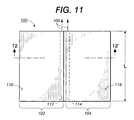
- Fig. 11 is a top plan view of
device 100, similar to the devices of Figs. 3-6, 9, and 10, except thatmetal contacts Lasers - Although the technique has not yet been tested experimentally, it has been simulated based on the dimensions and other parameters shown in the schematic, distorted cross-sectional view in Fig. 12, taken along the line 12-12' in Fig. 11. The simulation assumed that
device 100 had a threshold current of 14 mA, differential efficiency of 47%, operating current of 25 mA, and operating voltage of 1.8 V. - The lowest layer in Fig. 12 is
heat sink 200, which can include any suitable material at any suitable thickness. Betweenheat sink 200 andsubstrate 120 is a 2 µm layer of solder that holds the two together, deposited at 0.57 W/cm-K. Substrate 120 is a GaAs substrate 90 µm thick, deposited at 0.45 W/cm-K. The first epitaxial layer onsubstrate 120 is a 4 µm n-doped cladding layer deposited at 0.11 W/cm-K.Active layers lasers K. Laser stripes portions K. Lasers portions electrodes lasers layer 226 has a thickness of Z1, whilelayer 236 has a thickness of Z2. - The simulation produced the following temperature differences for values of Z1 and Z2: for Z1=1 µm and Z2=2 µm, the temperature difference was 0.4° C; for Z1=1 µm and Z2=3 µm, the temperature difference was 0.6° C; and for Z1=0.5 µm and Z2=1 µm, the temperature difference was 0.3° C.
- Fig. 13 shows a simulated thermal profile. The graph of Fig. 13 shows temperature along a line through the center of the active regions of
lasers laser 104, with Z2 = 3 µm; the right peak shows temperature withinlaser 102, with Z1 = 1 µm. The operating current for both lasers is 28 mA. A 0.6 degree C temperature difference between the two lasers is induced by the difference in thermal resistance, according to this simulation. - The technique of Figs. 9-11, if it can be successfully implemented, may also be applicable if different electrode materials or different layers of materials are used in the two lasers. Another variation would be to make the electrodes thicker only along part of the length of a laser stripe or to add non-electrode thermal conducting material along part of the length of a laser stripe. Additional thermal conducting material would provide another path for thermal current out of the laser in addition to the path provided by the electrode material.
- Fig. 14 shows a stage in producing
device 100 as in Figs. 11 and 12. In Fig. 14, an array of lasers has been fabricated on a surface ofwafer 250, which can be the material ofsubstrate 120.Exemplary lasers metal contacts metal contacts lead structure 260 has also been fabricated on the surface ofwafer 250, connected tolaser 254'smetal contact 118 and to the counterpart metal contact of each of the other laser pairs in the array. - A part, component, surface, or other element is described herein as "plated" if it was produced by plating or removing material, such as by electroless plating, electroplating, electroetching, or other electrodeposition or removal. For example, electroplating, electroetching, or other electrodeposition or removal may be performed on the structure in Fig. 14, such as by immersing the array of lasers on the surface of
wafer 250 in an electroplating solution or an electroetching bath or by an appropriate dry electroprocess. During this stage, an appropriate voltage Vplate is applied to leadstructure 260 at the periphery ofwafer 250, controlling the rate of electroactivity; an alternative approach would be to contact each laser's metal contact pad individually with a matching probe card. By measuring the current and/or time duration of the process, the amount of the material added or removed frommetal contact 254 can be controlled. - During plating, special attention must be paid to ensure that plated metal does not bridge across the gap between a pair of lasers, typically approximately 3 µm. Bridging could even occur between
stripes - When the desired difference in thickness between metal contacts of each pair of lasers has been produced,
wafer 250 can be sawed into chips.Lead structure 260 can be removed in the saw kerfs. Conventional steps can then be taken to package each pair of lasers and provide appropriate connections to electrical circuitry. - The technique of Fig. 14 is advantageous because it does not require a mask to produce a difference in current flow structure between lasers. It can also be extended to devices with more than two lasers, by repeating a similar step for all but one of the lasers on the chip. Various materials could be used in this process to enhance the difference in thermal conductance between lasers.
- Figs. 15 and 16 show another approach in which
high resistance material 280 is put betweenmetal contact 118 andlaser stripe 114, illustratively along a length similar to that of the cutout area in Fig. 9. A pattern of insulating material similar to the cutout areas in Fig. 10 could also be used.High resistance material 280 could be a dielectric such as an oxide or nitride or a partially conductive material such as amorphous silicon; in any case, it must make an area betweenmetal contact 118 andlaser stripe 114 more resistive than areas in which it is not present. - The technique in Figs. 15 and 16 would require additional masks and additional process steps, and therefore may be more expensive to implement than the techniques described for implementing Fig. 9.
- Fig. 17 illustrates quad
spot laser device 300 withlaser stripes metal contacts device 300 can be understood from U.S. Patent No. 6,052,399, incorporated herein by reference. In such a structure, adjacent laser elements are more likely to phase lock and produce hatching than laser elements that are farther apart.Device 300 might be operated so that some combinations of adjacent laser elements are phase locked, while others do not. - The implementation in Fig. 17 is intended to affect phase locking between certain combinations of lasers by patterning insulating
material 320 differently betweenmetal contact 314 andlaser stripe 302 than betweenmetal contact 316 andlaser stripe 308. As can be seen, more oflaser stripe 308 is covered by insulatingmaterial 320 than oflaser stripe 302, with the total covered amount being roughly 25% of the length of the laser stripes. - The technique of Fig. 17 is not limited to a quad spot device, but could be applied to other multiple spot laser devices. In addition, other techniques described herein could similarly be applied to quad spot or other multiple spot laser devices.
- Figs. 18 and 19 show yet another approach in which current flow is modified differently in different lasers, by modifying or, in a sense,
damaging region 340 of the epitaxial semiconductor structure to have more carrier traps, such as by growingregion 340 to have higher resistance or by ion implantation to increase resistance. Distribution of ions, such as hydrogen or oxygen, would not be confined to a sharp boundary, but would have a Gaussian-like distribution profile, with the depth depending on ion species, implant energy, and on the ease with which ions pass through the layers.Region 340 illustratively extends along a length similar to that of the cutout area in Fig. 9, but pattern of insulating material similar to the cutout areas in Fig. 10 could also be used. As in Figs. 15 and 16,region 340 must make an area more resistive than areas in which it is not present. - As in the case of Figures 15 and 16, the technique in Figs. 18 and 19 would require additional masks and additional process steps, and therefore may be more expensive to implement than the techniques described for implementing Fig.9.
- The implementations described above could be modified in various ways within the scope of the invention. For example, the above implementations generally involve closely spaced edge emitting lasers but the techniques could be used in other types of lasers, and it is foreseeable that other types of lasers will be developed in which the techniques could be used. Similarly, the above implementations generally involve semiconductor structures with particular geometries and dimensions, but the techniques could be used with other geometries and dimensions. Similarly, the above implementations involve types of lasers that typically emit in the infrared region, but the same or similar techniques could be used in lasers that emit in other regions of the spectrum, including the visible and ultraviolet regions.
- Some of the above exemplary implementations involve specific materials, such as specific semiconductor materials and metals, but the invention could be implemented with a wide variety of materials, including various substrates and other support structures, various semiconductor materials, and various conductive materials. For example, rather than being GaAs-based, the lasers could be based on any other suitable semiconductor material, with appropriate modifications; for gallium nitride semiconductors, for example, the substrate would typically be nonconductive, so that all contacts would be at or above the surface rather than through the substrate as is possible with GaAs. Similarly, other conductive materials could be used in current flow structures, including various metals, alloys, and conductive metal oxides, such as indium-tin-oxide; it might also be possible to use doped semiconductor materials such as heavily doped amorphous silicon.
- In addition to the specific current flow structures and types of differences described above, various other types of current flow structures could be used, including structures with additional layers and with different shapes, for example. Also, rather than having a difference between current flow structures, other types of wavelength control structures could be used to obtain a required difference in wavelength, such as gratings on a surface of a semiconductor structure or other techniques that differentially alter or adjust optical properties of lasers. For example, some conventional techniques etch epitaxial material or otherwise modify a surface to modulate refractive index, creating a grating that defines a waveguide mode allowing only one wavelength.
- The above exemplary implementations generally involve production of structures following particular operations, but different operations could be performed, the order of the operations could be modified, and additional operations could be added within the scope of the invention. For example, semiconductor structures that satisfy a semiconductor symmetry constraint could be formed in other ways than by concurrent epitaxial growth followed by concurrent patterning.
- Devices and structures like those described above have a wide range of applications. A semiconductor laser can, for example, be packaged in a can with wire bonds connecting pads of the lasers through the can's lid, and then can would then be appropriately mounted, such as on a board that also holds drive circuitry and other controller circuitry. Such devices can be used, as noted above, in printers, and could also be used in CD or DVD recorders, in laser projectors, or in various other applications, including foreseeable future applications.
- Further, rather than preventing phase locking, techniques for controlling wavelength as described above could be applied to affect phase locking in various other ways; for example, such techniques could be used to induce or control phase locking. Also, techniques that affect wavelength or produce wavelength differences as described above could be applied in ways other than to affect phase locking; for example, such techniques could be used to address other cross-talk issues.
Claims (10)
- A device comprising:a support structure; andat least two lasers on the support structure, each including:a semiconductor structure that emits light in response to stimulation; the semiconductor structures of a subset of two or more of the lasers including the same semiconductor material and having substantially the same geometry; anda current flow structure that affects current flow through the laser's semiconductor structure; the current flow structures of a pair of lasers in the subset being differently structured to affect wavelengths of light emitted from the semiconductor structures of the pair of lasers.
- The device of claim 1 in which the device comprises two lasers on the support structure.
- The device of claim 1 in which the device comprises four lasers on the support structure.
- The device of claim 1 in which the pair of lasers are concurrently operated.
- The device of claim 1 in which each of the pair of lasers is an edge-emitting laser.
- The device of claim 1 in which the pair of lasers are adjacent on a surface of the support structure.
- Apparatus comprising:a laser device that includes:a support structure; andat least two lasers on the support structure, each including:a semiconductor structure that emits light in response to stimulation; the semiconductor structures of a subset of two or more of the lasers including the same semiconductor material and having substantially the same geometry; anda current flow structure that affects current flow through the laser's semiconductor structure; anddrive circuitry that drives each of a pair of lasers in the subset within a respective range of operating conditions;the current flow structures of the pair of lasers being differently structured to affect wavelengths of light emitted from the semiconductor structures of the pair of lasers when each is driven within its respective range of operating conditions.
- A device comprising:a support structure; andat least two lasers on the support structure, each including:a semiconductor structure that emits light in response to stimulation; the semiconductor structures of a subset of two or more of the lasers including the same semiconductor material and having substantially the same geometry; anda wavelength control structure that affects the wavelength at which the laser's semiconductor structure emits light; the wavelength control structures of a pair of lasers in the subset being different so that the wavelengths at which the pair of lasers emit differ by at least a required difference in wavelength.
- A device comprising:a support structure; andat least two lasers on the support structure, each including:in each laser, the contact structure and the semiconductor structure providing a conductive path between the emitting region and an external component; the conductive paths in first and second lasers in the subset having different characteristics that affect the wavelengths of light emitted by the emitting regions of the first and second lasers.a semiconductor structure with an emitting region that emits light in response to stimulation; the semiconductor structures of a subset of two or more of the lasers being substantially identical; anda contact structure electrically or thermally connected to the semiconductor structure;
- A method of producing a device, comprising:on a support structure, producing at least two lasers, each including:a semiconductor structure that emits light in response to stimulation; anda current flow structure that affects current flow through the laser's semiconductor structure;the act of producing the lasers comprising:producing the semiconductor structures of a subset of the lasers to include the same semiconductor material and have substantially the same geometry; andproducing the current flow structures of a pair of lasers in the subset with different structures to affect wavelengths of light emitted by the semiconductor structures of the pair of lasers.
Applications Claiming Priority (1)
| Application Number | Priority Date | Filing Date | Title |
|---|---|---|---|
| US11/015,990 US7310358B2 (en) | 2004-12-17 | 2004-12-17 | Semiconductor lasers |
Publications (3)
| Publication Number | Publication Date |
|---|---|
| EP1672758A2 true EP1672758A2 (en) | 2006-06-21 |
| EP1672758A3 EP1672758A3 (en) | 2009-01-28 |
| EP1672758B1 EP1672758B1 (en) | 2016-06-29 |
Family
ID=36143692
Family Applications (1)
| Application Number | Title | Priority Date | Filing Date |
|---|---|---|---|
| EP05112234.9A Active EP1672758B1 (en) | 2004-12-17 | 2005-12-15 | Semiconductor lasers |
Country Status (3)
| Country | Link |
|---|---|
| US (1) | US7310358B2 (en) |
| EP (1) | EP1672758B1 (en) |
| JP (1) | JP5270066B2 (en) |
Families Citing this family (7)
| Publication number | Priority date | Publication date | Assignee | Title |
|---|---|---|---|---|
| ITMI20070271A1 (en) * | 2007-02-14 | 2008-08-15 | St Microelectronics Srl | PROCESS FOR PEER MANUFACTURING A TFT DEVICE WITH SOURCE AND DAIN REGIONS HAVING A GRADUAL PROFILE |
| US7951688B2 (en) * | 2007-10-01 | 2011-05-31 | Fairchild Semiconductor Corporation | Method and structure for dividing a substrate into individual devices |
| DE102008013896A1 (en) * | 2007-12-21 | 2009-06-25 | Osram Opto Semiconductors Gmbh | Laser light source |
| DE102008058436B4 (en) * | 2008-11-21 | 2019-03-07 | Osram Opto Semiconductors Gmbh | Edge-emitting semiconductor laser chip |
| JP5369795B2 (en) * | 2009-03-18 | 2013-12-18 | 日本電気株式会社 | Surface emitting laser array |
| US20140042470A1 (en) * | 2012-08-09 | 2014-02-13 | Epistar Corporation | Method of making light emitting device and light emitting device made thereof |
| WO2022258756A1 (en) * | 2021-06-11 | 2022-12-15 | Osram Opto Semiconductors Gmbh | Semiconductor chip and component |
Citations (1)
| Publication number | Priority date | Publication date | Assignee | Title |
|---|---|---|---|---|
| US4831629A (en) | 1987-09-01 | 1989-05-16 | Xerox Corporation | Incoherent, optically coupled laser arrays with increased spectral width |
Family Cites Families (21)
| Publication number | Priority date | Publication date | Assignee | Title |
|---|---|---|---|---|
| NL8101409A (en) * | 1981-03-23 | 1982-10-18 | Philips Nv | SEMICONDUCTOR LASER WITH AT LEAST TWO RADIATION BEAMS, AND METHOD OF MANUFACTURING THESE. |
| JPS6332986A (en) * | 1986-07-25 | 1988-02-12 | Mitsubishi Electric Corp | Integrated semiconductor laser |
| US4870652A (en) | 1988-07-08 | 1989-09-26 | Xerox Corporation | Monolithic high density arrays of independently addressable semiconductor laser sources |
| JPH02260482A (en) * | 1989-03-31 | 1990-10-23 | Canon Inc | Semiconductor laser device |
| US4980893A (en) * | 1989-05-25 | 1990-12-25 | Xerox Corporation | Monolithic high density arrays of independently addressable offset semiconductor laser sources |
| JP2748754B2 (en) * | 1991-12-03 | 1998-05-13 | 三菱電機株式会社 | Semiconductor optical device |
| US5513200A (en) * | 1992-09-22 | 1996-04-30 | Xerox Corporation | Monolithic array of independently addressable diode lasers |
| US5436193A (en) * | 1993-11-02 | 1995-07-25 | Xerox Corporation | Method of fabricating a stacked active region laser array |
| US5386428A (en) * | 1993-11-02 | 1995-01-31 | Xerox Corporation | Stacked active region laser array for multicolor emissions |
| JPH08107254A (en) * | 1994-09-14 | 1996-04-23 | Xerox Corp | Multiwavelength laser diode array |
| US5812576A (en) * | 1996-08-26 | 1998-09-22 | Xerox Corporation | Loss-guided semiconductor lasers |
| US5764676A (en) * | 1996-09-26 | 1998-06-09 | Xerox Corporation | Transversely injected multiple wavelength diode laser array formed by layer disordering |
| US6052399A (en) | 1997-08-29 | 2000-04-18 | Xerox Corporation | Independently addressable laser array with native oxide for optical confinement and electrical isolation |
| US6058124A (en) * | 1997-11-25 | 2000-05-02 | Xerox Corporation | Monolithic independently addressable Red/IR side by side laser |
| US6136623A (en) | 1998-05-06 | 2000-10-24 | Xerox Corporation | Multiple wavelength laser arrays by flip-chip bonding |
| US6744800B1 (en) | 1998-12-30 | 2004-06-01 | Xerox Corporation | Method and structure for nitride based laser diode arrays on an insulating substrate |
| KR100727907B1 (en) * | 2000-07-20 | 2007-06-14 | 삼성전자주식회사 | Multi-wavelength vertical cavity surface emitting laser and method for manufacturing thereof |
| KR100754156B1 (en) * | 2000-08-23 | 2007-09-03 | 삼성전자주식회사 | Multiple wavelength vertical-cavity surface emitting laser and method for manufacturing thereof |
| JP4126873B2 (en) * | 2000-12-20 | 2008-07-30 | 松下電器産業株式会社 | Semiconductor laser device |
| JPWO2003005514A1 (en) * | 2001-07-02 | 2004-10-28 | 古河電気工業株式会社 | Semiconductor laser device, semiconductor laser module, and optical fiber amplifier using semiconductor laser module |
| US20050105577A1 (en) * | 2003-11-13 | 2005-05-19 | Matsushita Electric Industrial Co., Ltd. | Semiconductor laser device and manufacturing method for the same |
-
2004
- 2004-12-17 US US11/015,990 patent/US7310358B2/en active Active
-
2005
- 2005-12-15 JP JP2005361202A patent/JP5270066B2/en active Active
- 2005-12-15 EP EP05112234.9A patent/EP1672758B1/en active Active
Patent Citations (1)
| Publication number | Priority date | Publication date | Assignee | Title |
|---|---|---|---|---|
| US4831629A (en) | 1987-09-01 | 1989-05-16 | Xerox Corporation | Incoherent, optically coupled laser arrays with increased spectral width |
Also Published As
| Publication number | Publication date |
|---|---|
| US20060133443A1 (en) | 2006-06-22 |
| JP2006173625A (en) | 2006-06-29 |
| JP5270066B2 (en) | 2013-08-21 |
| EP1672758A3 (en) | 2009-01-28 |
| EP1672758B1 (en) | 2016-06-29 |
| US7310358B2 (en) | 2007-12-18 |
Similar Documents
| Publication | Publication Date | Title |
|---|---|---|
| EP1672758B1 (en) | Semiconductor lasers | |
| Hasnain et al. | Performance of gain-guided surface emitting lasers with semiconductor distributed Bragg reflectors | |
| Chang-Hasnain et al. | Multiple wavelength tunable surface-emitting laser arrays | |
| Ackley | Single longitudinal mode operation of high power multiple‐stripe injection lasers | |
| KR940001793B1 (en) | Electrically pumped vertical cavity laser | |
| CA1228664A (en) | Phase-locked laser array having a non-uniform spacing between lasing regions | |
| Macomber et al. | Surface‐emitting distributed feedback semiconductor laser | |
| EP0390167B1 (en) | Semiconductor laser device having plurality of layers for emitting lights of different wavelengths and method of driving the same | |
| US20040065893A1 (en) | Semiconductor light-emitting device, method for fabricating the same, and method for driving the same | |
| JPH11135893A (en) | Edge-emitting laser | |
| Geels et al. | Design and characterization of In/sub 0.2/Ga/sub 0.8/As MQW vertical-cavity surface-emitting lasers | |
| Marsh et al. | Quantum well intermixing in material systems for 1.5 μm | |
| US5870419A (en) | Double heterojunction semiconductor laser having improved light confinement | |
| Lu et al. | Beyond 20 GHz bandwidth of partly gain-coupled 1.55 μm strained multiquantum well DFB lasers | |
| US5157681A (en) | Wavelength-tunable distributed Bragg reflector semiconductor laser | |
| Yuasa et al. | Characteristics of molecular‐beam epitaxially grown pair‐groove‐substrate GaAs/AlGaAs multiquantum‐well lasers | |
| Behringer | High-power diode laser technology and characteristics | |
| WO2021239407A1 (en) | Semiconductor laser with a horizontal laser element and a vertical laser element, lidar system and production method | |
| US10243330B2 (en) | Optoelectronic device with resonant suppression of high order optical modes and method of making same | |
| US6967770B2 (en) | Semiconductor optical amplifier with reduced effects of gain saturation | |
| EP0386634A1 (en) | Semiconductor laser device | |
| Deng et al. | Transverse and temporal mode dependence on mirror contrast in microcavity lasers | |
| JPH0724324B2 (en) | Semiconductor laser chip and manufacturing method thereof | |
| Kasraian et al. | Single‐lobed far‐field radiation pattern from surface‐emitting complex‐coupled distributed‐feedback diode lasers | |
| CA1267713A (en) | Semiconductor laser device |
Legal Events
| Date | Code | Title | Description |
|---|---|---|---|
| PUAI | Public reference made under article 153(3) epc to a published international application that has entered the european phase |
Free format text: ORIGINAL CODE: 0009012 |
|
| AK | Designated contracting states |
Kind code of ref document: A2 Designated state(s): AT BE BG CH CY CZ DE DK EE ES FI FR GB GR HU IE IS IT LI LT LU LV MC NL PL PT RO SE SI SK TR |
|
| AX | Request for extension of the european patent |
Extension state: AL BA HR MK YU |
|
| PUAL | Search report despatched |
Free format text: ORIGINAL CODE: 0009013 |
|
| AK | Designated contracting states |
Kind code of ref document: A3 Designated state(s): AT BE BG CH CY CZ DE DK EE ES FI FR GB GR HU IE IS IT LI LT LU LV MC NL PL PT RO SE SI SK TR |
|
| AX | Request for extension of the european patent |
Extension state: AL BA HR MK YU |
|
| RIC1 | Information provided on ipc code assigned before grant |
Ipc: H01S 5/042 20060101ALI20081222BHEP Ipc: H01S 5/40 20060101AFI20060425BHEP |
|
| 17P | Request for examination filed |
Effective date: 20090728 |
|
| AKX | Designation fees paid |
Designated state(s): DE FR GB |
|
| 17Q | First examination report despatched |
Effective date: 20090907 |
|
| GRAP | Despatch of communication of intention to grant a patent |
Free format text: ORIGINAL CODE: EPIDOSNIGR1 |
|
| INTG | Intention to grant announced |
Effective date: 20160314 |
|
| GRAS | Grant fee paid |
Free format text: ORIGINAL CODE: EPIDOSNIGR3 |
|
| GRAA | (expected) grant |
Free format text: ORIGINAL CODE: 0009210 |
|
| AK | Designated contracting states |
Kind code of ref document: B1 Designated state(s): DE FR GB |
|
| REG | Reference to a national code |
Ref country code: GB Ref legal event code: FG4D |
|
| REG | Reference to a national code |
Ref country code: DE Ref legal event code: R096 Ref document number: 602005049606 Country of ref document: DE |
|
| REG | Reference to a national code |
Ref country code: FR Ref legal event code: PLFP Year of fee payment: 12 |
|
| REG | Reference to a national code |
Ref country code: DE Ref legal event code: R097 Ref document number: 602005049606 Country of ref document: DE |
|
| PLBE | No opposition filed within time limit |
Free format text: ORIGINAL CODE: 0009261 |
|
| STAA | Information on the status of an ep patent application or granted ep patent |
Free format text: STATUS: NO OPPOSITION FILED WITHIN TIME LIMIT |
|
| 26N | No opposition filed |
Effective date: 20170330 |
|
| STAA | Information on the status of an ep patent application or granted ep patent |
Free format text: STATUS: NO OPPOSITION FILED WITHIN TIME LIMIT |
|
| REG | Reference to a national code |
Ref country code: FR Ref legal event code: PLFP Year of fee payment: 13 |
|
| PGFP | Annual fee paid to national office [announced via postgrant information from national office to epo] |
Ref country code: GB Payment date: 20231121 Year of fee payment: 19 |
|
| PGFP | Annual fee paid to national office [announced via postgrant information from national office to epo] |
Ref country code: FR Payment date: 20231122 Year of fee payment: 19 Ref country code: DE Payment date: 20231121 Year of fee payment: 19 |