EP1672654A1 - Microelectromechanical System Actuator - Google Patents
Microelectromechanical System Actuator Download PDFInfo
- Publication number
- EP1672654A1 EP1672654A1 EP05105264A EP05105264A EP1672654A1 EP 1672654 A1 EP1672654 A1 EP 1672654A1 EP 05105264 A EP05105264 A EP 05105264A EP 05105264 A EP05105264 A EP 05105264A EP 1672654 A1 EP1672654 A1 EP 1672654A1
- Authority
- EP
- European Patent Office
- Prior art keywords
- comb
- piezoelectric
- movable comb
- actuator
- substrate
- Prior art date
- Legal status (The legal status is an assumption and is not a legal conclusion. Google has not performed a legal analysis and makes no representation as to the accuracy of the status listed.)
- Granted
Links
- 239000000758 substrate Substances 0.000 claims abstract description 33
- 239000000463 material Substances 0.000 claims abstract description 25
- 239000010410 layer Substances 0.000 claims description 43
- 239000000919 ceramic Substances 0.000 claims description 18
- 239000002184 metal Substances 0.000 claims description 14
- 229910052751 metal Inorganic materials 0.000 claims description 14
- 239000011247 coating layer Substances 0.000 claims description 12
- 239000013078 crystal Substances 0.000 claims description 12
- 229910004243 O3-PbTiO3 Inorganic materials 0.000 claims description 3
- 229910004293 O3—PbTiO3 Inorganic materials 0.000 claims description 3
- 229910020215 Pb(Mg1/3Nb2/3)O3PbTiO3 Inorganic materials 0.000 claims description 3
- 230000003287 optical effect Effects 0.000 abstract description 6
- 230000009977 dual effect Effects 0.000 abstract description 4
- XUIMIQQOPSSXEZ-UHFFFAOYSA-N Silicon Chemical compound [Si] XUIMIQQOPSSXEZ-UHFFFAOYSA-N 0.000 description 10
- 229910052710 silicon Inorganic materials 0.000 description 10
- 239000010703 silicon Substances 0.000 description 10
- 210000001520 comb Anatomy 0.000 description 8
- 238000006073 displacement reaction Methods 0.000 description 6
- 239000011810 insulating material Substances 0.000 description 6
- 238000004519 manufacturing process Methods 0.000 description 6
- 230000008901 benefit Effects 0.000 description 5
- 229910052737 gold Inorganic materials 0.000 description 3
- 238000000034 method Methods 0.000 description 3
- 229910010293 ceramic material Inorganic materials 0.000 description 2
- 238000005229 chemical vapour deposition Methods 0.000 description 2
- 239000002178 crystalline material Substances 0.000 description 2
- HFGPZNIAWCZYJU-UHFFFAOYSA-N lead zirconate titanate Chemical compound [O-2].[O-2].[O-2].[O-2].[O-2].[Ti+4].[Zr+4].[Pb+2] HFGPZNIAWCZYJU-UHFFFAOYSA-N 0.000 description 2
- 238000003754 machining Methods 0.000 description 2
- 239000004065 semiconductor Substances 0.000 description 2
- 238000004088 simulation Methods 0.000 description 2
- 229910000975 Carbon steel Inorganic materials 0.000 description 1
- 239000004593 Epoxy Substances 0.000 description 1
- 238000013016 damping Methods 0.000 description 1
- 230000004907 flux Effects 0.000 description 1
- 239000011521 glass Substances 0.000 description 1
- 230000004048 modification Effects 0.000 description 1
- 238000012986 modification Methods 0.000 description 1
- 230000008569 process Effects 0.000 description 1
- 239000002210 silicon-based material Substances 0.000 description 1
- 238000004544 sputter deposition Methods 0.000 description 1
- 239000000725 suspension Substances 0.000 description 1
- 238000004804 winding Methods 0.000 description 1
Images



Classifications
-
- G—PHYSICS
- G11—INFORMATION STORAGE
- G11B—INFORMATION STORAGE BASED ON RELATIVE MOVEMENT BETWEEN RECORD CARRIER AND TRANSDUCER
- G11B9/00—Recording or reproducing using a method not covered by one of the main groups G11B3/00 - G11B7/00; Record carriers therefor
- G11B9/12—Recording or reproducing using a method not covered by one of the main groups G11B3/00 - G11B7/00; Record carriers therefor using near-field interactions; Record carriers therefor
- G11B9/14—Recording or reproducing using a method not covered by one of the main groups G11B3/00 - G11B7/00; Record carriers therefor using near-field interactions; Record carriers therefor using microscopic probe means, i.e. recording or reproducing by means directly associated with the tip of a microscopic electrical probe as used in Scanning Tunneling Microscopy [STM] or Atomic Force Microscopy [AFM] for inducing physical or electrical perturbations in a recording medium; Record carriers or media specially adapted for such transducing of information
-
- H—ELECTRICITY
- H01—ELECTRIC ELEMENTS
- H01H—ELECTRIC SWITCHES; RELAYS; SELECTORS; EMERGENCY PROTECTIVE DEVICES
- H01H1/00—Contacts
- H01H1/0036—Switches making use of microelectromechanical systems [MEMS]
-
- H—ELECTRICITY
- H01—ELECTRIC ELEMENTS
- H01H—ELECTRIC SWITCHES; RELAYS; SELECTORS; EMERGENCY PROTECTIVE DEVICES
- H01H57/00—Electrostrictive relays; Piezoelectric relays
-
- H—ELECTRICITY
- H01—ELECTRIC ELEMENTS
- H01H—ELECTRIC SWITCHES; RELAYS; SELECTORS; EMERGENCY PROTECTIVE DEVICES
- H01H59/00—Electrostatic relays; Electro-adhesion relays
- H01H59/0009—Electrostatic relays; Electro-adhesion relays making use of micromechanics
-
- H—ELECTRICITY
- H01—ELECTRIC ELEMENTS
- H01H—ELECTRIC SWITCHES; RELAYS; SELECTORS; EMERGENCY PROTECTIVE DEVICES
- H01H57/00—Electrostrictive relays; Piezoelectric relays
- H01H2057/006—Micromechanical piezoelectric relay
Definitions
- the present invention relates to a microelectromechanical system (MEMS) actuator and, more particularly, to a MEMS actuator that a cantilever piezoelectric actuator and a comb actuator are combined to perform dual shaft drive.
- MEMS actuator can be used in a driving apparatus of an ultra-slim optical disk drive.
- a conventional actuator used in an optical pickup driving apparatus is a voice coil motor (VCM) actuator including a magnetic circuit for applying a magnetic flux to a coil to generate a Lorentz force, a bobbin for fixing the coil and optical parts, a wire suspension for supporting the bobbin and damping vibrations transmitted to the bobbin, and a printed circuit board (PCB) for transmitting input and output signals of a servo system and supplying current to the coil
- VCM voice coil motor
- PCB printed circuit board
- a single shaft control ultra-small actuator mainly uses a MEMS comb actuator or a cantilever piezoelectric actuator depending on purpose.
- the comb actuator using an electrostatic force applies a voltage to a pair of combs perpendicularly projected from a planar surface and inserted into each other so that the electrostatic force generated between the two combs uniformly produces power depending on relative movement between the combs.
- the electrostatic comb-drive actuator has an advantage of providing uniform power with respect to movement of one comb.
- the cantilever piezoelectric actuator is manufactured mostly using PZT ceramic, and used in various fields that a microscopic location control apparatus is required
- This actuator has an advantage capable of readily performing precise control since displacement of the actuator is determined depending on a driving voltage applied to a piezoelectric material.
- it is possible to compose the ultra-fine actuator since its displacement can be controlled by tens of' nanometers.
- the cantilever piezoelectric actuator has been used for obtaining and controlling ultra-fine driving force such as driving force of an atomic force microscope (AFM), a nano drive actuator, a MEMS structure and so on
- the conventional actuators have disadvantages that only single shaft can be controlled, its application range is limited, especially, the piezoelectric actuator should have high drive voltage in order to obtain large displacement using the PZT ceramic, and therefore, it is difficult to manufacture the actuators in a small size.
- the present invention is directed to an ultra-small dual shaft control MEMS actuator that can be used in an ultra-small mobile driving apparatus requiring dual shaft control.
- the present invention is also directed to an ultra-small MEMS actuator capable of adapting a semiconductor manufacturing process, different from a conventional VCM actuator.
- the present invention is also directed to an actuator capable of simultaneously performing tracking and focusing drive by adapting a cantilever beam single crystalline piezoelectric actuator as a drive part of a comb actuator, being one-step advanced from the piezoelectric actuator located at a center portion of a conventional head to perform the tracking drive only.
- the present invention is also directed to an actuator capable of performing focusing drive of large displacement even at a low voltage.
- One aspect of the present invention is to provide a MEMS actuator including: a stationary comb fixed on a substrate; a movable comb disposed separately from the substrate; and a spring connected to the movable comb and the substrate to resiliently support the movable comb, wherein the movable comb includes a piezoelectric material layer in a laminated manner to be perpendicularly moved by piezoelectric phenomenon and laterally moved by electrostatic force to the stationary comb.
- the movable comb includes metal coating layers, and the piezoelectric material layer interposed between the metal coating layers, and the MEMS actuator may further include a post for fixing the stationary comb on the substrate.
- the stationary comb and the movable comb including the piezoelectric material layer have an advantage that the MEMS actuator can be manufactured by a more simple process.
- the piezoelectric material layer may use one of a piezoelectric ceramic layer and a piezoelectric single crystalline layer
- the piezoelectric material layer may use one selected from PZT ceramic, PMN-PT(Pb(Mg 1/3 Nb 2/3 )O 3 -PbTiO 3 ) ceramic, and PZN-PT(Pb(Zn 1/3 Nb 2/3 )O 3 -PbTiO 3 ) ceramic
- the piezoelectric single crystalline layer may use one of a PMN-PT single crystal and a PZN-PT single crystal.
- the spring supporting the movable comb may be formed at only one end of' the movable comb to move the other end of the movable comb using the spring as a shaft to thereby increase mobility of the movable comb
- FIG. 1 is a schematic plan view of' a MEMS actuator in accordance with an embodiment of the present invention
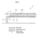
- FIGS. 2 and 3 are cross-sectional views taken along the lines AA' and BB' of the MEMS actuator shown in FIG 1, respectively;
- FIG 4 is a graph representing a result of simulation of the actuator of FIG 2.
- FIG. 1 is a schematic plan view of a MEMS actuator in accordance with an embodiment of the present invention
- FIGS 2 and 3 are cross-sectional views taken along the lines AA' and BB' of' the MEMS actuator shown in FIG 1, respectively.
- the MEMS actuator includes a stationary comb 10 fixed on a substrate (not shown), a movable comb 11 disposed separately from the substrate, and a spring 12 connected to the movable comb 11 and the substrate to movably support the movable comb 11.
- the movable comb 11 includes a piezoelectric material layer formed in a laminated manner to be perpendicularly moved by a piezoelectric phenomenon, and laterally moved by an electrostatic force to the stationary comb
- the piezoelectric material may use one of a piezoelectric ceramic layer and a piezoelectric single crystalline layer
- the piezoelectric ceramic layer may use one selected from PZT ceramic, PMN-PT(Pb(Mg 1/3 Nb 2/3 )O 3 -PbTiO 3 ) ceramic, and PZN-PT(Pb(Zn 1/3 Nb 2/3 )O 3 -PbTiO 3 ) ceramic
- the piezoelectric single crystalline layer may use one of a PMN-PT single crystal and a PZN-PT single crystal
- the stationary comb 10 is disposed at both sides of the movable comb 11 separated from the substrate and alternately inserted to be spaced apart from the movable comb 11.
- a post 13 may be additionally installed in order to fix the spring 12 and the substrate That is, the spring 12 spaced apart from the substrate is connected to the post 13 to movably and resiliently support the movable comb 11.
- the piezoelectric material layer of the movable comb 11 is made of a piezoelectric single crystalline material or a piezoelectric ceramic material to produce a piezoelectric phenomenon
- the stationary comb 10, the post 13 and the spring 12 may also include an insulating material formed in a laminated manner and having piezoelectric characteristics.
- the stationary comb 10, the post 13 and the spring 12 are configured not to produce the piezoelectric phenomenon since a voltage difference is not applied between upper and lower parts of' the insulating material layer
- the stationary comb 10, the movable comb 11, the post 13 and the spring 12 may include an insulating material layer (not shown) formed on the substrate in a laminated manner
- the post 13 is spaced apart from the movable comb 11 to be disposed at one side of the movable comb 11 and fixed to a silicon substrate The other side of the movable comb 11, at which the post 13 is not disposed, can be readily moved.
- the stationary comb 10 includes, for example, a stationary stage 101 fixed to the silicon substrate, and a plurality of stationary fingers 102 projected from one side of the stationary stage 101 in a comb shape
- the movable comb 11 is spaced apart from the silicon substrate to be straightly moved, and includes a plurality of' movable fingers 112 projected from both sides of a movable stage 111 in a comb shape
- the movable stage 111 faces the plurality of stationary fingers 102
- the stationary comb 10 and the movable comb 11 are physically and electrically separated from each other, and the stationary fingers 102 and the movable fingers 112 are alternately inserted to be spaced apart from each other.
- a voltage is applied between the pair of combs alternately inserted into each other to allow the electrostatic force generated between the two combs to uniformly produce power with respect to relative movement between the both combs.
- the spring 12 is disposed between the post 13 and the movable comb 11, and separated from the silicon substrate. That is, one end of the spring 12 is connected to the post 13, and the other end is connected to one end of the movable comb 11, thereby resiliently supporting the movable comb 11.
- FIGS. 2 and 3 are cross-sectional views taken along the lines AA' and BB' of the MEMS actuator shown in FIG 1, respectively.
- the movable comb 11 is formed on a substrate 14 in a floated manner, and includes an elastic layer 111a, a lower electrode 111b, an insulating material 111d having piezoelectric characteristics, and an upper electrode 111c Conductive metal coating layers are formed of the lower and upper electrodes 111b and 111c.
- the metal coating layer is made of one of Al and Au
- the movable comb 11, the post 13 for fixing the substrate 14, and the spring 12 for resiliently supporting the post 13 and the movable comb 11 may be made of a silicon material,
- the substrate is preferably a silicon substrate, it is possible to substitute with a substrate made of a different material, for example, a glass substrate, having good machining characteristics, for the silicon substrate
- Upper electrodes 111c and 101c are formed on the insulating material of the stationary comb 10 and the movable comb 11 to apply a voltage
- the lower electrode 101b of the stationary comb 10 is inserted for the convenience of the manufacturing process, the lower electrode 101b may be omitted
- the lower electrode 111b of a metal coating layer is formed on the elastic layer 111a
- the upper electrode 111c is formed on a piezoelectric material layer of a piezoelectric single crystalline material layer or a piezoelectric ceramic material layer
- the metal coating layer may be formed of Al or Au and formed to a thickness of about 0.5 ⁇ m using a chemical vapor deposition (CVD) method or a sputtering method.
- the elastic layers 12, 13, 111a and 101a may be manufactured using a portion of the silicon surface or plain carbon steel
- the stationary comb 10 is symmetrically disposed at both sides of the movable comb 11 and voltages of polarity opposite to each other are applied to the combs 10 and 11 to make the electrostatic force between the electrodes of the movable comb 11 and the stationary comb 10 larger, thereby laterally driving the movable comb 11 to perform the tracking drive using the electrostatic force between the combs.
- a movable stage 111 of the movable comb 11 may be operated by a cantilever beam piezoelectric actuator.
- the substrate 14 and the insulating material layer 111d having piezoelectric characteristics may be directly deposited or adhered by epoxy.
- the electrodes have a conductive metal layer coated on lower and upper surfaces of' the piezoelectric ceramic layer or the piezoelectric single crystal layer to provide the cantilever beam piezoelectric actuator
- the metal coating layer is made of' Al or Au widely used in a semiconductor manufacturing process.
- a poling direction formed by the piezoelectric material layer 111d is perpendicularly directed to a surface of the movable stage 111. Therefore, when the voltage is applied to the upper and lower surfaces of the piezoelectric material layer, volume of the piezoelectric material layer expands in lateral and longitudinal directions depending on each piezoelectric charge constant. At this time, the lower surface of the piezoelectric material layer is fixed to the silicon substrate to prevent the volume from expanding. As a result, the cantilever beam is bent up and down to perform the focusing drive. At this time, the silicon substrate functions as an elastic layer, and may be substituted with a material having excellent machining characteristics and high elastic coefficient
- FIG. 4 is a graph representing a result of simulation of the actuator of FIG 2
- the graph is an analyzed result of PZT-8 ceramic, PMN-33%PT single crystals and PZN-8%PI single crystals with respect to an actuator including a cantilever beam having a length of 12 mm and a width of 2 mm, a piezoelectric layer having a thickness of' 150 ⁇ m and a silicon substrate having a thickness of 40 ⁇ m, using a finite element method (FEM)
- FEM finite element method
- Tip displacement of' the cantilever beam with respect to the voltage of 10 V applied to the upper and lower surfaces of' the piezoelectric material layer was 49.7 ⁇ m in the case of the PZN-8%PT single crystals, 46.0 ⁇ m in the case of the PMN-33%PT single crystals, and 299 ⁇ m in the case of the PZT-8 ceramic.
- the cantilever beam piezoelectric actuator in accordance with the present invention adapts the piezoelectric single crystal to enable large displacement at a low drive voltage, and adapts the movable comb stage to simultaneously perform the focusing drive as well as the tracking drive.
- the actuator in accordance with the present invention may be applied as a core part of an ultra-small mobile drive apparatus requiring dual-shaft control.
- the actuator in accordance with the present invention is appropriate to use in an ultra-small mobile optical disk drive apparatus having a thickness of not more than about 5 mm, since the actuator used in the ultra-small mobile optical disk drive should satisfy low power drive conditions and the actuator should have a small volume.
- the actuator may be adapted to any apparatus requiring an ultra-small low power dual-shaft position control.
Landscapes
- Physics & Mathematics (AREA)
- Electromagnetism (AREA)
- Micromachines (AREA)
- Optical Recording Or Reproduction (AREA)
- Mechanical Light Control Or Optical Switches (AREA)
- General Electrical Machinery Utilizing Piezoelectricity, Electrostriction Or Magnetostriction (AREA)
Abstract
Description
- This application claims priority to and the benefit of Korean Patent Application No. 2004-107033, filed December 16, 2004, the disclosure of which is incorporated herein by reference in its entirety.
- The present invention relates to a microelectromechanical system (MEMS) actuator and, more particularly, to a MEMS actuator that a cantilever piezoelectric actuator and a comb actuator are combined to perform dual shaft drive. The MEMS actuator can be used in a driving apparatus of an ultra-slim optical disk drive.
- A conventional actuator used in an optical pickup driving apparatus is a voice coil motor (VCM) actuator including a magnetic circuit for applying a magnetic flux to a coil to generate a Lorentz force, a bobbin for fixing the coil and optical parts, a wire suspension for supporting the bobbin and damping vibrations transmitted to the bobbin, and a printed circuit board (PCB) for transmitting input and output signals of a servo system and supplying current to the coil However, it is difficult to manufacture the conventional VCM actuator in an ultra-small size due to a structure that the bobbin for winding the coil, a support member for supporting the bobbin, and the magnetic circuit including a magnet, a yoke plate and so on should be required
- A single shaft control ultra-small actuator mainly uses a MEMS comb actuator or a cantilever piezoelectric actuator depending on purpose.
- The comb actuator using an electrostatic force applies a voltage to a pair of combs perpendicularly projected from a planar surface and inserted into each other so that the electrostatic force generated between the two combs uniformly produces power depending on relative movement between the combs. The electrostatic comb-drive actuator has an advantage of providing uniform power with respect to movement of one comb.
- The cantilever piezoelectric actuator is manufactured mostly using PZT ceramic, and used in various fields that a microscopic location control apparatus is required This actuator has an advantage capable of readily performing precise control since displacement of the actuator is determined depending on a driving voltage applied to a piezoelectric material. In particular, it is possible to compose the ultra-fine actuator since its displacement can be controlled by tens of' nanometers. The cantilever piezoelectric actuator has been used for obtaining and controlling ultra-fine driving force such as driving force of an atomic force microscope (AFM), a nano drive actuator, a MEMS structure and so on
- However, the conventional actuators have disadvantages that only single shaft can be controlled, its application range is limited, especially, the piezoelectric actuator should have high drive voltage in order to obtain large displacement using the PZT ceramic, and therefore, it is difficult to manufacture the actuators in a small size.
- The present invention is directed to an ultra-small dual shaft control MEMS actuator that can be used in an ultra-small mobile driving apparatus requiring dual shaft control.
- The present invention is also directed to an ultra-small MEMS actuator capable of adapting a semiconductor manufacturing process, different from a conventional VCM actuator.
- The present invention is also directed to an actuator capable of simultaneously performing tracking and focusing drive by adapting a cantilever beam single crystalline piezoelectric actuator as a drive part of a comb actuator, being one-step advanced from the piezoelectric actuator located at a center portion of a conventional head to perform the tracking drive only.
- The present invention is also directed to an actuator capable of performing focusing drive of large displacement even at a low voltage.
- One aspect of the present invention is to provide a MEMS actuator including: a stationary comb fixed on a substrate; a movable comb disposed separately from the substrate; and a spring connected to the movable comb and the substrate to resiliently support the movable comb, wherein the movable comb includes a piezoelectric material layer in a laminated manner to be perpendicularly moved by piezoelectric phenomenon and laterally moved by electrostatic force to the stationary comb.
- Preferably, the movable comb includes metal coating layers, and the piezoelectric material layer interposed between the metal coating layers, and the MEMS actuator may further include a post for fixing the stationary comb on the substrate.
- In addition, the stationary comb and the movable comb including the piezoelectric material layer have an advantage that the MEMS actuator can be manufactured by a more simple process. Preferably, the piezoelectric material layer may use one of a piezoelectric ceramic layer and a piezoelectric single crystalline layer, the piezoelectric material layer may use one selected from PZT ceramic, PMN-PT(Pb(Mg1/3Nb2/3)O3-PbTiO3) ceramic, and PZN-PT(Pb(Zn1/3Nb2/3)O3-PbTiO3) ceramic, and the piezoelectric single crystalline layer may use one of a PMN-PT single crystal and a PZN-PT single crystal.
- Meanwhile, the spring supporting the movable comb may be formed at only one end of' the movable comb to move the other end of the movable comb using the spring as a shaft to thereby increase mobility of the movable comb
- The above and other features and advantages of' the present invention will become more apparent to those of ordinary skill in the art by describing in detail exemplary embodiments thereof with reference to the attached drawings in which:
- FIG. 1 is a schematic plan view of' a MEMS actuator in accordance with an embodiment of the present invention;
- FIGS. 2 and 3 are cross-sectional views taken along the lines AA' and BB' of the MEMS actuator shown in FIG 1, respectively; and
- FIG 4 is a graph representing a result of simulation of the actuator of FIG 2.
- The present invention will now be described more fully hereinafter with reference to the accompanying drawings, in which preferred embodiments of the invention are shown. This invention may, however, be embodied in different forms and should not be construed as limited to the embodiments set forth herein. Rather, these embodiments are provided so that this disclosure will be thorough and complete, and will fully convey the scope of the invention to those skilled in the art.
- FIG. 1 is a schematic plan view of a MEMS actuator in accordance with an embodiment of the present invention, and FIGS 2 and 3 are cross-sectional views taken along the lines AA' and BB' of' the MEMS actuator shown in FIG 1, respectively.
- Referring to FIG 1, the MEMS actuator includes a
stationary comb 10 fixed on a substrate (not shown), amovable comb 11 disposed separately from the substrate, and aspring 12 connected to themovable comb 11 and the substrate to movably support themovable comb 11. Themovable comb 11 includes a piezoelectric material layer formed in a laminated manner to be perpendicularly moved by a piezoelectric phenomenon, and laterally moved by an electrostatic force to the stationary comb The piezoelectric material may use one of a piezoelectric ceramic layer and a piezoelectric single crystalline layer The piezoelectric ceramic layer may use one selected from PZT ceramic, PMN-PT(Pb(Mg1/3Nb2/3)O3-PbTiO3) ceramic, and PZN-PT(Pb(Zn1/3Nb2/3)O3-PbTiO3) ceramic, and the piezoelectric single crystalline layer may use one of a PMN-PT single crystal and a PZN-PT single crystal - More specifically describing, the
stationary comb 10 is disposed at both sides of themovable comb 11 separated from the substrate and alternately inserted to be spaced apart from themovable comb 11. In addition, apost 13 may be additionally installed in order to fix thespring 12 and the substrate That is, thespring 12 spaced apart from the substrate is connected to thepost 13 to movably and resiliently support themovable comb 11. - The piezoelectric material layer of the
movable comb 11 is made of a piezoelectric single crystalline material or a piezoelectric ceramic material to produce a piezoelectric phenomenon For the convenience of the manufacturing process, thestationary comb 10, thepost 13 and thespring 12 may also include an insulating material formed in a laminated manner and having piezoelectric characteristics. In this case, thestationary comb 10, thepost 13 and thespring 12 are configured not to produce the piezoelectric phenomenon since a voltage difference is not applied between upper and lower parts of' the insulating material layer Thestationary comb 10, themovable comb 11, thepost 13 and thespring 12 may include an insulating material layer (not shown) formed on the substrate in a laminated manner - The
post 13 is spaced apart from themovable comb 11 to be disposed at one side of themovable comb 11 and fixed to a silicon substrate The other side of themovable comb 11, at which thepost 13 is not disposed, can be readily moved. - The
stationary comb 10 includes, for example, astationary stage 101 fixed to the silicon substrate, and a plurality ofstationary fingers 102 projected from one side of thestationary stage 101 in a comb shape Themovable comb 11 is spaced apart from the silicon substrate to be straightly moved, and includes a plurality of'movable fingers 112 projected from both sides of amovable stage 111 in a comb shape Here, themovable stage 111 faces the plurality ofstationary fingers 102 - The
stationary comb 10 and themovable comb 11 are physically and electrically separated from each other, and thestationary fingers 102 and themovable fingers 112 are alternately inserted to be spaced apart from each other. A voltage is applied between the pair of combs alternately inserted into each other to allow the electrostatic force generated between the two combs to uniformly produce power with respect to relative movement between the both combs. - The
spring 12 is disposed between thepost 13 and themovable comb 11, and separated from the silicon substrate. That is, one end of thespring 12 is connected to thepost 13, and the other end is connected to one end of themovable comb 11, thereby resiliently supporting themovable comb 11. - FIGS. 2 and 3 are cross-sectional views taken along the lines AA' and BB' of the MEMS actuator shown in FIG 1, respectively.
- The
movable comb 11 is formed on asubstrate 14 in a floated manner, and includes anelastic layer 111a, alower electrode 111b, aninsulating material 111d having piezoelectric characteristics, and anupper electrode 111c Conductive metal coating layers are formed of the lower andupper electrodes movable comb 11, thepost 13 for fixing thesubstrate 14, and thespring 12 for resiliently supporting thepost 13 and themovable comb 11 may be made of a silicon material, - While the substrate is preferably a silicon substrate, it is possible to substitute with a substrate made of a different material, for example, a glass substrate, having good machining characteristics, for the silicon substrate
Upper electrodes stationary comb 10 and themovable comb 11 to apply a voltage In this case, when the voltage is not applied to alower electrode 101b of thestationary comb 10, a voltage difference is not applied to apiezoelectric material layer 101d. Since thelower electrode 101b of thestationary comb 10 is inserted for the convenience of the manufacturing process, thelower electrode 101b may be omitted - Specifically, the
lower electrode 111b of a metal coating layer is formed on theelastic layer 111a, and theupper electrode 111c is formed on a piezoelectric material layer of a piezoelectric single crystalline material layer or a piezoelectric ceramic material layer, and the metal coating layer may be formed of Al or Au and formed to a thickness of about 0.5 µm using a chemical vapor deposition (CVD) method or a sputtering method. - Meanwhile, the
elastic layers - Next, operation of the MEMS actuator in accordance with an embodiment of the present invention will be described.
- Referring to FIGS. 1 to 3, when a DC voltage (for example, - 5V) is uniformly applied to the metal coating layer of the
movable comb 11, and a voltage (for example, 10V) having a polarity alternately varied as time goes is applied to the metal layer of a leftstationary comb 10, an attractive electrostatic force is generated between the metal coating layers to allow themovable comb 11 to be pulled toward the leftstationary comb 10. At this time, elasticity of thespring 12 and intensity of the voltage applied to the metal coating layer may be adjusted to control a moving distance of themovable comb 11, - When the voltage applied to the electrodes is cut off, the
movable comb 11 is recovered to its original state by a restoration force of the spring At this time, when a voltage having equal intensity and opposite polarity to the voltage applied to the electrode of the leftstationary comb 10 is applied to a rightstationary comb 10, a repulsive electrostatic force is generated between themovable comb 11 and the rightstationary comb 10 to allow themovable comb 11 to be more pushed toward the left side - As described above, the
stationary comb 10 is symmetrically disposed at both sides of themovable comb 11 and voltages of polarity opposite to each other are applied to thecombs movable comb 11 and thestationary comb 10 larger, thereby laterally driving themovable comb 11 to perform the tracking drive using the electrostatic force between the combs. - Meanwhile, a
movable stage 111 of themovable comb 11 may be operated by a cantilever beam piezoelectric actuator. As shown in FIG. 3, thesubstrate 14 and theinsulating material layer 111d having piezoelectric characteristics may be directly deposited or adhered by epoxy. In addition, the electrodes have a conductive metal layer coated on lower and upper surfaces of' the piezoelectric ceramic layer or the piezoelectric single crystal layer to provide the cantilever beam piezoelectric actuator Preferably, the metal coating layer is made of' Al or Au widely used in a semiconductor manufacturing process. - Preferably, a poling direction formed by the
piezoelectric material layer 111d is perpendicularly directed to a surface of themovable stage 111. Therefore, when the voltage is applied to the upper and lower surfaces of the piezoelectric material layer, volume of the piezoelectric material layer expands in lateral and longitudinal directions depending on each piezoelectric charge constant. At this time, the lower surface of the piezoelectric material layer is fixed to the silicon substrate to prevent the volume from expanding. As a result, the cantilever beam is bent up and down to perform the focusing drive. At this time, the silicon substrate functions as an elastic layer, and may be substituted with a material having excellent machining characteristics and high elastic coefficient - FIG. 4 is a graph representing a result of simulation of the actuator of FIG 2
- The graph is an analyzed result of PZT-8 ceramic, PMN-33%PT single crystals and PZN-8%PI single crystals with respect to an actuator including a cantilever beam having a length of 12 mm and a width of 2 mm, a piezoelectric layer having a thickness of' 150 µm and a silicon substrate having a thickness of 40 µm, using a finite element method (FEM)
- Tip displacement of' the cantilever beam with respect to the voltage of 10 V applied to the upper and lower surfaces of' the piezoelectric material layer was 49.7 µm in the case of the PZN-8%PT single crystals, 46.0 µm in the case of the PMN-33%PT single crystals, and 299 µm in the case of the PZT-8 ceramic.
- As can be seen from the foregoing, the cantilever beam piezoelectric actuator in accordance with the present invention adapts the piezoelectric single crystal to enable large displacement at a low drive voltage, and adapts the movable comb stage to simultaneously perform the focusing drive as well as the tracking drive.
- The actuator in accordance with the present invention may be applied as a core part of an ultra-small mobile drive apparatus requiring dual-shaft control.
- The actuator in accordance with the present invention is appropriate to use in an ultra-small mobile optical disk drive apparatus having a thickness of not more than about 5 mm, since the actuator used in the ultra-small mobile optical disk drive should satisfy low power drive conditions and the actuator should have a small volume.
- In addition, the actuator may be adapted to any apparatus requiring an ultra-small low power dual-shaft position control.
- Although exemplary embodiments of the present invention have been described with reference to the attached drawings, the present invention is not limited to these embodiments, and it should be appreciated to those skilled in the art that a variety of modifications and changes can be made without departing from the spirit and scope of the present invention.
Claims (7)
- A microelectromechanical system (MEMS) actuator comprising:a stationary comb fixed on a substrate;a movable comb disposed separately from the substrate; anda spring connected to the movable comb and the substrate to resiliently support the movable comb,wherein the movable comb includes a piezoelectric material layer in a laminated manner to be perpendicularly moved by a piezoelectric phenomenon and laterally moved by an electrostatic force to the stationary comb.
- The MEMS actuator according to claim 1, wherein the movable comb comprises metal coating layers, and the piezoelectric material layer is interposed between the metal coating layers.
- The MEMS actuator according to claim 1 or 2, further comprising a post for fixing the stationary comb on the substrate.
- The MEMS actuator according to claim .3, wherein the stationary comb and the movable comb comprises the piezoelectric material layer.
- The MEMS actuator according to one of claims 1 to 4, wherein the piezoelectric material layer is one of' a piezoelectric ceramic layer and a piezoelectric single crystalline layer.
- The MEMS actuator according to claim 5, wherein the piezoelectric material layer is made of one selected from PZT ceramic, PMN-PI(Pb(Mg1/3Nb2/3)O3-PbTiO3) ceramic, and PZN-PT(Pb(Zn1/3Nb2/3)O3-PbTiO3) ceramic, and the piezoelectric single crystalline layer is made of one of a PMN-PT single crystal and a PZN-PT single crystal.
- The MEMS actuator according to one of claims 1 to 6, wherein the spring supporting the movable comb is formed at only one end of the movable comb
Applications Claiming Priority (1)
| Application Number | Priority Date | Filing Date | Title |
|---|---|---|---|
| KR1020040107033A KR100639918B1 (en) | 2004-12-16 | 2004-12-16 | MEMS Actuator |
Publications (2)
| Publication Number | Publication Date |
|---|---|
| EP1672654A1 true EP1672654A1 (en) | 2006-06-21 |
| EP1672654B1 EP1672654B1 (en) | 2007-08-15 |
Family
ID=35520919
Family Applications (1)
| Application Number | Title | Priority Date | Filing Date |
|---|---|---|---|
| EP05105264A Expired - Lifetime EP1672654B1 (en) | 2004-12-16 | 2005-06-15 | Microelectromechanical System Actuator |
Country Status (8)
| Country | Link |
|---|---|
| US (1) | US7242129B2 (en) |
| EP (1) | EP1672654B1 (en) |
| JP (1) | JP2006174688A (en) |
| KR (1) | KR100639918B1 (en) |
| AT (1) | ATE370505T1 (en) |
| DE (1) | DE602005002010T2 (en) |
| SG (1) | SG123655A1 (en) |
| TW (1) | TWI286122B (en) |
Cited By (5)
| Publication number | Priority date | Publication date | Assignee | Title |
|---|---|---|---|---|
| WO2009153757A1 (en) * | 2008-06-19 | 2009-12-23 | Nxp B.V. | Piezoelectric bimorph switch |
| US7835115B2 (en) * | 2003-07-29 | 2010-11-16 | Meyer Dallas W | Integrated recording head with selective movement |
| US7849585B1 (en) | 2004-04-05 | 2010-12-14 | Meyer Dallas W | Micropositioning recording head for a magnetic storage device |
| US8279559B1 (en) | 2009-01-02 | 2012-10-02 | Meyer Dallas W | Process for creating discrete track magnetic recording media including an apparatus having a stylus selectively applying stress to a surface of the recording media |
| WO2022271135A3 (en) * | 2021-06-22 | 2023-06-01 | Pamukkale Universitesi | A mems comb finger resonator coating method |
Families Citing this family (20)
| Publication number | Priority date | Publication date | Assignee | Title |
|---|---|---|---|---|
| KR100639918B1 (en) * | 2004-12-16 | 2006-11-01 | 한국전자통신연구원 | MEMS Actuator |
| KR100726436B1 (en) * | 2005-07-27 | 2007-06-11 | 삼성전자주식회사 | MEMS switch driven by electrostatic force and piezoelectric force |
| FR2897486B1 (en) * | 2006-02-13 | 2011-07-22 | Commissariat Energie Atomique | VARIABLE REMOTE ENERGY REMOTE ENERGY CONVERSION SYSTEM AND ENERGY RECOVERY METHOD |
| IL183692A0 (en) * | 2007-06-05 | 2007-09-20 | Nova Measuring Instr Ltd | Apparatus and method for substrates handling |
| US7586239B1 (en) * | 2007-06-06 | 2009-09-08 | Rf Micro Devices, Inc. | MEMS vibrating structure using a single-crystal piezoelectric thin film layer |
| US9369105B1 (en) | 2007-08-31 | 2016-06-14 | Rf Micro Devices, Inc. | Method for manufacturing a vibrating MEMS circuit |
| US9385685B2 (en) | 2007-08-31 | 2016-07-05 | Rf Micro Devices, Inc. | MEMS vibrating structure using an orientation dependent single-crystal piezoelectric thin film layer |
| US9391588B2 (en) | 2007-08-31 | 2016-07-12 | Rf Micro Devices, Inc. | MEMS vibrating structure using an orientation dependent single-crystal piezoelectric thin film layer |
| US10170685B2 (en) | 2008-06-30 | 2019-01-01 | The Regents Of The University Of Michigan | Piezoelectric MEMS microphone |
| KR101606780B1 (en) * | 2008-06-30 | 2016-03-28 | 더 리젠츠 오브 더 유니버시티 오브 미시건 | Piezoelectric memes microphone |
| US7732975B1 (en) * | 2008-12-29 | 2010-06-08 | Formfactor, Inc. | Biased gap-closing actuator |
| US9117593B2 (en) | 2012-11-02 | 2015-08-25 | Rf Micro Devices, Inc. | Tunable and switchable resonator and filter structures in single crystal piezoelectric MEMS devices using bimorphs |
| CN103594617A (en) * | 2013-11-29 | 2014-02-19 | 上海集成电路研发中心有限公司 | Piezoelectric cantilever sensor and manufacturing method thereof |
| US9991872B2 (en) | 2014-04-04 | 2018-06-05 | Qorvo Us, Inc. | MEMS resonator with functional layers |
| US9998088B2 (en) | 2014-05-02 | 2018-06-12 | Qorvo Us, Inc. | Enhanced MEMS vibrating device |
| JP6488657B2 (en) * | 2014-11-12 | 2019-03-27 | 株式会社リコー | Actuator |
| TWI621582B (en) * | 2015-08-14 | 2018-04-21 | 先進微系統科技股份有限公司 | Comb-shaped actuator |
| US12091313B2 (en) | 2019-08-26 | 2024-09-17 | The Research Foundation For The State University Of New York | Electrodynamically levitated actuator |
| US20210144483A1 (en) * | 2019-11-07 | 2021-05-13 | Innovative Interface Laboratory Corp. | Single-axis actuator, acoustic wave generator and its array |
| US11634320B2 (en) * | 2021-02-22 | 2023-04-25 | Taiwan Semiconductor Manufacturing Company Limited | Micro-electromechanical system device including a precision proof mass element and methods for forming the same |
Citations (4)
| Publication number | Priority date | Publication date | Assignee | Title |
|---|---|---|---|---|
| JPH05147762A (en) * | 1991-11-25 | 1993-06-15 | Mitsubishi Electric Corp | Sheet transport device |
| US5223762A (en) * | 1990-12-27 | 1993-06-29 | Murata Manufacturing Co., Ltd. | Surface acoustic wave filter |
| US20020089254A1 (en) * | 1999-11-23 | 2002-07-11 | Mcnc | Miniature electrical relays using a piezoelectric thin film as an actuating element |
| US20040075366A1 (en) * | 2002-10-21 | 2004-04-22 | Hrl Laboratories, Llc | Piezoelectric switch for tunable electronic components |
Family Cites Families (14)
| Publication number | Priority date | Publication date | Assignee | Title |
|---|---|---|---|---|
| JP3450349B2 (en) | 1992-03-31 | 2003-09-22 | キヤノン株式会社 | Cantilever probe |
| US6472794B1 (en) * | 1992-07-10 | 2002-10-29 | Matsushita Electric Industrial Co., Ltd. | Microactuator |
| WO1998027547A1 (en) | 1996-12-16 | 1998-06-25 | Seagate Technology, Inc. | Bimorph piezoelectric microactuator head and flexure assembly |
| JPH1114634A (en) | 1997-06-24 | 1999-01-22 | Hitachi Ltd | Control device |
| JPH11322424A (en) | 1998-05-20 | 1999-11-24 | Matsushita Electric Ind Co Ltd | Piezoelectric material and piezoelectric vibrator, sound generator, sound detector, actuator and piezoelectric transformer using the same |
| US20010040419A1 (en) * | 2000-03-24 | 2001-11-15 | Behrang Behin | Biased rotatable combdrive sensor methods |
| JP4095439B2 (en) | 2000-10-20 | 2008-06-04 | 富士通株式会社 | Piezoelectric actuator |
| US6483056B2 (en) * | 2000-10-27 | 2002-11-19 | Daniel J Hyman | Microfabricated relay with multimorph actuator and electrostatic latch mechanism |
| FR2835981B1 (en) * | 2002-02-13 | 2005-04-29 | Commissariat Energie Atomique | TUNABLE VOLUME MEMS ACOUSTIC WAVE MICRORESONATOR |
| EP1505663A4 (en) | 2002-05-15 | 2009-08-19 | Seiko Epson Corp | PIEZOELECTRIC ACTUATOR AND INKJET HEAD |
| KR100468853B1 (en) | 2002-08-30 | 2005-01-29 | 삼성전자주식회사 | MEMS comb actuator materialized on insulating material and method of manufacturing thereof |
| JP3907628B2 (en) | 2003-02-07 | 2007-04-18 | キヤノン株式会社 | Piezoelectric actuator, manufacturing method thereof, and liquid discharge head |
| KR100639918B1 (en) * | 2004-12-16 | 2006-11-01 | 한국전자통신연구원 | MEMS Actuator |
| KR100815362B1 (en) * | 2005-01-05 | 2008-03-19 | 삼성전기주식회사 | Interdigitate diffraction type optical modulator |
-
2004
- 2004-12-16 KR KR1020040107033A patent/KR100639918B1/en not_active Expired - Fee Related
-
2005
- 2005-06-15 AT AT05105264T patent/ATE370505T1/en not_active IP Right Cessation
- 2005-06-15 EP EP05105264A patent/EP1672654B1/en not_active Expired - Lifetime
- 2005-06-15 DE DE602005002010T patent/DE602005002010T2/en not_active Expired - Lifetime
- 2005-06-21 US US11/157,745 patent/US7242129B2/en not_active Expired - Fee Related
- 2005-06-21 TW TW094120527A patent/TWI286122B/en active
- 2005-06-24 SG SG200504101A patent/SG123655A1/en unknown
- 2005-07-26 JP JP2005216098A patent/JP2006174688A/en active Pending
Patent Citations (4)
| Publication number | Priority date | Publication date | Assignee | Title |
|---|---|---|---|---|
| US5223762A (en) * | 1990-12-27 | 1993-06-29 | Murata Manufacturing Co., Ltd. | Surface acoustic wave filter |
| JPH05147762A (en) * | 1991-11-25 | 1993-06-15 | Mitsubishi Electric Corp | Sheet transport device |
| US20020089254A1 (en) * | 1999-11-23 | 2002-07-11 | Mcnc | Miniature electrical relays using a piezoelectric thin film as an actuating element |
| US20040075366A1 (en) * | 2002-10-21 | 2004-04-22 | Hrl Laboratories, Llc | Piezoelectric switch for tunable electronic components |
Non-Patent Citations (1)
| Title |
|---|
| PATENT ABSTRACTS OF JAPAN vol. 017, no. 541 (M - 1488) 29 September 1993 (1993-09-29) * |
Cited By (10)
| Publication number | Priority date | Publication date | Assignee | Title |
|---|---|---|---|---|
| US7835115B2 (en) * | 2003-07-29 | 2010-11-16 | Meyer Dallas W | Integrated recording head with selective movement |
| US8284524B2 (en) | 2003-07-29 | 2012-10-09 | Meyer Dallas W | Integrated recording head with selective movement |
| US9070413B2 (en) | 2003-07-29 | 2015-06-30 | Dallas W. Meyer | Integrated recording head with selective movement |
| US9659594B2 (en) | 2003-07-29 | 2017-05-23 | Dallas W. Meyer | Integrated recording head with selective movement |
| US7849585B1 (en) | 2004-04-05 | 2010-12-14 | Meyer Dallas W | Micropositioning recording head for a magnetic storage device |
| US8307542B2 (en) | 2004-04-05 | 2012-11-13 | Meyer Dallas W | Micropositioning recording head for a magnetic storage device |
| WO2009153757A1 (en) * | 2008-06-19 | 2009-12-23 | Nxp B.V. | Piezoelectric bimorph switch |
| US8847466B2 (en) | 2008-06-19 | 2014-09-30 | Nxp B.V. | Piezoelectric bimorph switch |
| US8279559B1 (en) | 2009-01-02 | 2012-10-02 | Meyer Dallas W | Process for creating discrete track magnetic recording media including an apparatus having a stylus selectively applying stress to a surface of the recording media |
| WO2022271135A3 (en) * | 2021-06-22 | 2023-06-01 | Pamukkale Universitesi | A mems comb finger resonator coating method |
Also Published As
| Publication number | Publication date |
|---|---|
| ATE370505T1 (en) | 2007-09-15 |
| DE602005002010T2 (en) | 2008-05-15 |
| TW200621620A (en) | 2006-07-01 |
| US20060131997A1 (en) | 2006-06-22 |
| DE602005002010D1 (en) | 2007-09-27 |
| SG123655A1 (en) | 2006-07-26 |
| EP1672654B1 (en) | 2007-08-15 |
| US7242129B2 (en) | 2007-07-10 |
| TWI286122B (en) | 2007-09-01 |
| KR100639918B1 (en) | 2006-11-01 |
| KR20060068370A (en) | 2006-06-21 |
| JP2006174688A (en) | 2006-06-29 |
Similar Documents
| Publication | Publication Date | Title |
|---|---|---|
| EP1672654B1 (en) | Microelectromechanical System Actuator | |
| KR100392908B1 (en) | Actuator, apparatus for recording and reproducing information, and method for manufacturing actuator | |
| US7486002B2 (en) | Lateral piezoelectric driven highly tunable micro-electromechanical system (MEMS) inductor | |
| EP1845608B1 (en) | Inertial drive actuator | |
| CN102187409B (en) | Coil part | |
| KR20060042979A (en) | Positioning device for precise operation | |
| CN114208006A (en) | Force-balanced micromirror with electromagnetic actuation | |
| KR20070073222A (en) | Micro Actuator and Data Storage Device Employing It | |
| WO2002077994A1 (en) | Actuator for positioning head element finely and head device with the actuator | |
| US8120231B2 (en) | Inertial drive actuator | |
| US20030117027A1 (en) | Low inertia latching microactuator | |
| US20070096602A1 (en) | Impact drive actuator and lens drive device using the same | |
| US7911299B2 (en) | Microactuator, optical apparatus, and optical switch | |
| JP2010035348A (en) | Electromagnetic drive type actuator and method of manufacturing same | |
| JP4562614B2 (en) | Nano tweezers | |
| US20040202094A1 (en) | Adjusting mechanism for flying pickup head in data storage device | |
| US20220380201A1 (en) | Microelectromechanical drive for moving objects | |
| CN110546774B (en) | How to Operate an Ultrasonic Motor | |
| KR100707207B1 (en) | Manufacturing method of micro actuator with media stage | |
| JP4562615B2 (en) | Micro sample gripping device | |
| JPH11252959A (en) | Piezoelectric actuator and method of manufacturing the same | |
| JP2607560B2 (en) | Linear actuator | |
| JPH11245135A (en) | Micro movement device | |
| JP2001339965A (en) | Piezo actuator | |
| JP2024073995A (en) | Vibration actuator and method for manufacturing the vibration actuator |
Legal Events
| Date | Code | Title | Description |
|---|---|---|---|
| PUAI | Public reference made under article 153(3) epc to a published international application that has entered the european phase |
Free format text: ORIGINAL CODE: 0009012 |
|
| AK | Designated contracting states |
Kind code of ref document: A1 Designated state(s): AT BE BG CH CY CZ DE DK EE ES FI FR GB GR HU IE IS IT LI LT LU MC NL PL PT RO SE SI SK TR |
|
| AX | Request for extension of the european patent |
Extension state: AL BA HR LV MK YU |
|
| 17P | Request for examination filed |
Effective date: 20061205 |
|
| GRAP | Despatch of communication of intention to grant a patent |
Free format text: ORIGINAL CODE: EPIDOSNIGR1 |
|
| AKX | Designation fees paid |
Designated state(s): AT BE BG CH CY CZ DE DK EE ES FI FR GB GR HU IE IS IT LI LT LU MC NL PL PT RO SE SI SK TR |
|
| RIN1 | Information on inventor provided before grant (corrected) |
Inventor name: KIM, SANG HYEOB Inventor name: KIM, KI CHUL Inventor name: KIM, HYE JIN Inventor name: CHO, DOO HEE |
|
| GRAS | Grant fee paid |
Free format text: ORIGINAL CODE: EPIDOSNIGR3 |
|
| GRAA | (expected) grant |
Free format text: ORIGINAL CODE: 0009210 |
|
| AK | Designated contracting states |
Kind code of ref document: B1 Designated state(s): AT BE BG CH CY CZ DE DK EE ES FI FR GB GR HU IE IS IT LI LT LU MC NL PL PT RO SE SI SK TR |
|
| REG | Reference to a national code |
Ref country code: GB Ref legal event code: FG4D |
|
| REG | Reference to a national code |
Ref country code: CH Ref legal event code: EP |
|
| REG | Reference to a national code |
Ref country code: IE Ref legal event code: FG4D |
|
| REF | Corresponds to: |
Ref document number: 602005002010 Country of ref document: DE Date of ref document: 20070927 Kind code of ref document: P |
|
| REG | Reference to a national code |
Ref country code: SE Ref legal event code: TRGR |
|
| REG | Reference to a national code |
Ref country code: CH Ref legal event code: NV Representative=s name: SCHMAUDER & PARTNER AG PATENTANWALTSBUERO |
|
| PG25 | Lapsed in a contracting state [announced via postgrant information from national office to epo] |
Ref country code: IS Free format text: LAPSE BECAUSE OF FAILURE TO SUBMIT A TRANSLATION OF THE DESCRIPTION OR TO PAY THE FEE WITHIN THE PRESCRIBED TIME-LIMIT Effective date: 20071215 Ref country code: ES Free format text: LAPSE BECAUSE OF FAILURE TO SUBMIT A TRANSLATION OF THE DESCRIPTION OR TO PAY THE FEE WITHIN THE PRESCRIBED TIME-LIMIT Effective date: 20071126 Ref country code: BG Free format text: LAPSE BECAUSE OF FAILURE TO SUBMIT A TRANSLATION OF THE DESCRIPTION OR TO PAY THE FEE WITHIN THE PRESCRIBED TIME-LIMIT Effective date: 20071115 Ref country code: LT Free format text: LAPSE BECAUSE OF FAILURE TO SUBMIT A TRANSLATION OF THE DESCRIPTION OR TO PAY THE FEE WITHIN THE PRESCRIBED TIME-LIMIT Effective date: 20070815 |
|
| PG25 | Lapsed in a contracting state [announced via postgrant information from national office to epo] |
Ref country code: AT Free format text: LAPSE BECAUSE OF FAILURE TO SUBMIT A TRANSLATION OF THE DESCRIPTION OR TO PAY THE FEE WITHIN THE PRESCRIBED TIME-LIMIT Effective date: 20070815 Ref country code: PL Free format text: LAPSE BECAUSE OF FAILURE TO SUBMIT A TRANSLATION OF THE DESCRIPTION OR TO PAY THE FEE WITHIN THE PRESCRIBED TIME-LIMIT Effective date: 20070815 |
|
| ET | Fr: translation filed | ||
| PG25 | Lapsed in a contracting state [announced via postgrant information from national office to epo] |
Ref country code: GR Free format text: LAPSE BECAUSE OF FAILURE TO SUBMIT A TRANSLATION OF THE DESCRIPTION OR TO PAY THE FEE WITHIN THE PRESCRIBED TIME-LIMIT Effective date: 20071116 Ref country code: DK Free format text: LAPSE BECAUSE OF FAILURE TO SUBMIT A TRANSLATION OF THE DESCRIPTION OR TO PAY THE FEE WITHIN THE PRESCRIBED TIME-LIMIT Effective date: 20070815 |
|
| PG25 | Lapsed in a contracting state [announced via postgrant information from national office to epo] |
Ref country code: SK Free format text: LAPSE BECAUSE OF FAILURE TO SUBMIT A TRANSLATION OF THE DESCRIPTION OR TO PAY THE FEE WITHIN THE PRESCRIBED TIME-LIMIT Effective date: 20070815 Ref country code: PT Free format text: LAPSE BECAUSE OF FAILURE TO SUBMIT A TRANSLATION OF THE DESCRIPTION OR TO PAY THE FEE WITHIN THE PRESCRIBED TIME-LIMIT Effective date: 20080115 Ref country code: CZ Free format text: LAPSE BECAUSE OF FAILURE TO SUBMIT A TRANSLATION OF THE DESCRIPTION OR TO PAY THE FEE WITHIN THE PRESCRIBED TIME-LIMIT Effective date: 20070815 |
|
| PLBE | No opposition filed within time limit |
Free format text: ORIGINAL CODE: 0009261 |
|
| STAA | Information on the status of an ep patent application or granted ep patent |
Free format text: STATUS: NO OPPOSITION FILED WITHIN TIME LIMIT |
|
| PG25 | Lapsed in a contracting state [announced via postgrant information from national office to epo] |
Ref country code: RO Free format text: LAPSE BECAUSE OF FAILURE TO SUBMIT A TRANSLATION OF THE DESCRIPTION OR TO PAY THE FEE WITHIN THE PRESCRIBED TIME-LIMIT Effective date: 20070815 |
|
| 26N | No opposition filed |
Effective date: 20080516 |
|
| PG25 | Lapsed in a contracting state [announced via postgrant information from national office to epo] |
Ref country code: MC Free format text: LAPSE BECAUSE OF NON-PAYMENT OF DUE FEES Effective date: 20080630 |
|
| PG25 | Lapsed in a contracting state [announced via postgrant information from national office to epo] |
Ref country code: IE Free format text: LAPSE BECAUSE OF NON-PAYMENT OF DUE FEES Effective date: 20080616 Ref country code: EE Free format text: LAPSE BECAUSE OF FAILURE TO SUBMIT A TRANSLATION OF THE DESCRIPTION OR TO PAY THE FEE WITHIN THE PRESCRIBED TIME-LIMIT Effective date: 20070815 |
|
| PG25 | Lapsed in a contracting state [announced via postgrant information from national office to epo] |
Ref country code: SI Free format text: LAPSE BECAUSE OF FAILURE TO SUBMIT A TRANSLATION OF THE DESCRIPTION OR TO PAY THE FEE WITHIN THE PRESCRIBED TIME-LIMIT Effective date: 20070815 |
|
| PG25 | Lapsed in a contracting state [announced via postgrant information from national office to epo] |
Ref country code: CY Free format text: LAPSE BECAUSE OF FAILURE TO SUBMIT A TRANSLATION OF THE DESCRIPTION OR TO PAY THE FEE WITHIN THE PRESCRIBED TIME-LIMIT Effective date: 20070815 |
|
| REG | Reference to a national code |
Ref country code: CH Ref legal event code: PCAR Free format text: SCHMAUDER & PARTNER AG PATENT- UND MARKENANWAELTE VSP;ZWAENGIWEG 7;8038 ZUERICH (CH) |
|
| PG25 | Lapsed in a contracting state [announced via postgrant information from national office to epo] |
Ref country code: LU Free format text: LAPSE BECAUSE OF NON-PAYMENT OF DUE FEES Effective date: 20080615 Ref country code: HU Free format text: LAPSE BECAUSE OF FAILURE TO SUBMIT A TRANSLATION OF THE DESCRIPTION OR TO PAY THE FEE WITHIN THE PRESCRIBED TIME-LIMIT Effective date: 20080216 |
|
| PG25 | Lapsed in a contracting state [announced via postgrant information from national office to epo] |
Ref country code: TR Free format text: LAPSE BECAUSE OF FAILURE TO SUBMIT A TRANSLATION OF THE DESCRIPTION OR TO PAY THE FEE WITHIN THE PRESCRIBED TIME-LIMIT Effective date: 20070815 |
|
| PGFP | Annual fee paid to national office [announced via postgrant information from national office to epo] |
Ref country code: FI Payment date: 20110331 Year of fee payment: 7 Ref country code: IT Payment date: 20110323 Year of fee payment: 7 |
|
| PGFP | Annual fee paid to national office [announced via postgrant information from national office to epo] |
Ref country code: FR Payment date: 20110420 Year of fee payment: 7 Ref country code: CH Payment date: 20110517 Year of fee payment: 7 Ref country code: BE Payment date: 20110330 Year of fee payment: 7 Ref country code: SE Payment date: 20110401 Year of fee payment: 7 |
|
| PGFP | Annual fee paid to national office [announced via postgrant information from national office to epo] |
Ref country code: GB Payment date: 20110401 Year of fee payment: 7 Ref country code: NL Payment date: 20110404 Year of fee payment: 7 |
|
| BERE | Be: lapsed |
Owner name: ELECTRONICS AND TELECOMMUNICATIONS RESEARCH INSTI Effective date: 20120630 |
|
| REG | Reference to a national code |
Ref country code: NL Ref legal event code: V1 Effective date: 20130101 |
|
| REG | Reference to a national code |
Ref country code: SE Ref legal event code: EUG |
|
| PG25 | Lapsed in a contracting state [announced via postgrant information from national office to epo] |
Ref country code: FI Free format text: LAPSE BECAUSE OF NON-PAYMENT OF DUE FEES Effective date: 20120615 |
|
| REG | Reference to a national code |
Ref country code: CH Ref legal event code: PL |
|
| REG | Reference to a national code |
Ref country code: CH Ref legal event code: PL |
|
| GBPC | Gb: european patent ceased through non-payment of renewal fee |
Effective date: 20120615 |
|
| PG25 | Lapsed in a contracting state [announced via postgrant information from national office to epo] |
Ref country code: IT Free format text: LAPSE BECAUSE OF NON-PAYMENT OF DUE FEES Effective date: 20120615 Ref country code: SE Free format text: LAPSE BECAUSE OF NON-PAYMENT OF DUE FEES Effective date: 20120616 |
|
| REG | Reference to a national code |
Ref country code: FR Ref legal event code: ST Effective date: 20130228 |
|
| REG | Reference to a national code |
Ref country code: DE Ref legal event code: R119 Ref document number: 602005002010 Country of ref document: DE Effective date: 20130101 |
|
| PG25 | Lapsed in a contracting state [announced via postgrant information from national office to epo] |
Ref country code: BE Free format text: LAPSE BECAUSE OF NON-PAYMENT OF DUE FEES Effective date: 20120630 Ref country code: CH Free format text: LAPSE BECAUSE OF NON-PAYMENT OF DUE FEES Effective date: 20120630 Ref country code: LI Free format text: LAPSE BECAUSE OF NON-PAYMENT OF DUE FEES Effective date: 20120630 Ref country code: NL Free format text: LAPSE BECAUSE OF NON-PAYMENT OF DUE FEES Effective date: 20130101 Ref country code: DE Free format text: LAPSE BECAUSE OF NON-PAYMENT OF DUE FEES Effective date: 20130101 Ref country code: FR Free format text: LAPSE BECAUSE OF NON-PAYMENT OF DUE FEES Effective date: 20120702 Ref country code: GB Free format text: LAPSE BECAUSE OF NON-PAYMENT OF DUE FEES Effective date: 20120615 |
|
| PGFP | Annual fee paid to national office [announced via postgrant information from national office to epo] |
Ref country code: DE Payment date: 20110330 Year of fee payment: 7 |