EP1670026A2 - Bilderzeugungsgerät - Google Patents
Bilderzeugungsgerät Download PDFInfo
- Publication number
- EP1670026A2 EP1670026A2 EP05026405A EP05026405A EP1670026A2 EP 1670026 A2 EP1670026 A2 EP 1670026A2 EP 05026405 A EP05026405 A EP 05026405A EP 05026405 A EP05026405 A EP 05026405A EP 1670026 A2 EP1670026 A2 EP 1670026A2
- Authority
- EP
- European Patent Office
- Prior art keywords
- electron
- high resistance
- spacer
- substrate
- film
- Prior art date
- Legal status (The legal status is an assumption and is not a legal conclusion. Google has not performed a legal analysis and makes no representation as to the accuracy of the status listed.)
- Granted
Links
- 125000006850 spacer group Chemical group 0.000 claims abstract description 86
- 239000000758 substrate Substances 0.000 claims abstract description 83
- 230000035515 penetration Effects 0.000 claims abstract description 33
- 238000009792 diffusion process Methods 0.000 claims abstract description 13
- 239000002184 metal Substances 0.000 claims description 9
- 229910052751 metal Inorganic materials 0.000 claims description 9
- 230000005484 gravity Effects 0.000 claims description 6
- 239000000203 mixture Substances 0.000 claims description 6
- 150000004767 nitrides Chemical class 0.000 claims description 4
- 230000002093 peripheral effect Effects 0.000 claims description 3
- 239000010408 film Substances 0.000 description 122
- 239000010410 layer Substances 0.000 description 24
- 238000000034 method Methods 0.000 description 23
- 239000000463 material Substances 0.000 description 12
- 238000005259 measurement Methods 0.000 description 11
- 238000010276 construction Methods 0.000 description 9
- 239000000969 carrier Substances 0.000 description 8
- 238000010894 electron beam technology Methods 0.000 description 7
- KFZMGEQAYNKOFK-UHFFFAOYSA-N Isopropanol Chemical compound CC(C)O KFZMGEQAYNKOFK-UHFFFAOYSA-N 0.000 description 6
- OAICVXFJPJFONN-UHFFFAOYSA-N Phosphorus Chemical compound [P] OAICVXFJPJFONN-UHFFFAOYSA-N 0.000 description 6
- BASFCYQUMIYNBI-UHFFFAOYSA-N platinum Substances [Pt] BASFCYQUMIYNBI-UHFFFAOYSA-N 0.000 description 5
- 238000010586 diagram Methods 0.000 description 4
- 238000009826 distribution Methods 0.000 description 4
- 239000011159 matrix material Substances 0.000 description 4
- 238000000611 regression analysis Methods 0.000 description 4
- 230000001186 cumulative effect Effects 0.000 description 3
- 238000005520 cutting process Methods 0.000 description 3
- 230000000694 effects Effects 0.000 description 3
- 239000011521 glass Substances 0.000 description 3
- KDLHZDBZIXYQEI-UHFFFAOYSA-N palladium Substances [Pd] KDLHZDBZIXYQEI-UHFFFAOYSA-N 0.000 description 3
- 239000002356 single layer Substances 0.000 description 3
- XOLBLPGZBRYERU-UHFFFAOYSA-N tin dioxide Chemical compound O=[Sn]=O XOLBLPGZBRYERU-UHFFFAOYSA-N 0.000 description 3
- CSCPPACGZOOCGX-UHFFFAOYSA-N Acetone Chemical compound CC(C)=O CSCPPACGZOOCGX-UHFFFAOYSA-N 0.000 description 2
- 238000010521 absorption reaction Methods 0.000 description 2
- 239000000919 ceramic Substances 0.000 description 2
- 238000000576 coating method Methods 0.000 description 2
- 239000003086 colorant Substances 0.000 description 2
- 230000006378 damage Effects 0.000 description 2
- 230000007812 deficiency Effects 0.000 description 2
- 238000006073 displacement reaction Methods 0.000 description 2
- 239000010931 gold Substances 0.000 description 2
- 230000003993 interaction Effects 0.000 description 2
- 238000007639 printing Methods 0.000 description 2
- 238000005001 rutherford backscattering spectroscopy Methods 0.000 description 2
- 238000004544 sputter deposition Methods 0.000 description 2
- 230000003746 surface roughness Effects 0.000 description 2
- OKTJSMMVPCPJKN-UHFFFAOYSA-N Carbon Chemical compound [C] OKTJSMMVPCPJKN-UHFFFAOYSA-N 0.000 description 1
- 229910005987 Ge3N4 Inorganic materials 0.000 description 1
- KJTLSVCANCCWHF-UHFFFAOYSA-N Ruthenium Chemical compound [Ru] KJTLSVCANCCWHF-UHFFFAOYSA-N 0.000 description 1
- VYPSYNLAJGMNEJ-UHFFFAOYSA-N Silicium dioxide Chemical compound O=[Si]=O VYPSYNLAJGMNEJ-UHFFFAOYSA-N 0.000 description 1
- 238000009825 accumulation Methods 0.000 description 1
- PNEYBMLMFCGWSK-UHFFFAOYSA-N aluminium oxide Inorganic materials [O-2].[O-2].[O-2].[Al+3].[Al+3] PNEYBMLMFCGWSK-UHFFFAOYSA-N 0.000 description 1
- 229910003481 amorphous carbon Inorganic materials 0.000 description 1
- 238000004458 analytical method Methods 0.000 description 1
- 238000013459 approach Methods 0.000 description 1
- 239000011230 binding agent Substances 0.000 description 1
- 229910052799 carbon Inorganic materials 0.000 description 1
- 238000004140 cleaning Methods 0.000 description 1
- 239000011248 coating agent Substances 0.000 description 1
- 238000007796 conventional method Methods 0.000 description 1
- 238000000151 deposition Methods 0.000 description 1
- 230000006866 deterioration Effects 0.000 description 1
- 238000007598 dipping method Methods 0.000 description 1
- 239000012789 electroconductive film Substances 0.000 description 1
- 229910052732 germanium Inorganic materials 0.000 description 1
- GNPVGFCGXDBREM-UHFFFAOYSA-N germanium atom Chemical compound [Ge] GNPVGFCGXDBREM-UHFFFAOYSA-N 0.000 description 1
- BIXHRBFZLLFBFL-UHFFFAOYSA-N germanium nitride Chemical compound N#[Ge]N([Ge]#N)[Ge]#N BIXHRBFZLLFBFL-UHFFFAOYSA-N 0.000 description 1
- PCHJSUWPFVWCPO-UHFFFAOYSA-N gold Chemical compound [Au] PCHJSUWPFVWCPO-UHFFFAOYSA-N 0.000 description 1
- 229910052737 gold Inorganic materials 0.000 description 1
- 239000012535 impurity Substances 0.000 description 1
- 238000009413 insulation Methods 0.000 description 1
- 239000011229 interlayer Substances 0.000 description 1
- 150000002500 ions Chemical class 0.000 description 1
- 230000001678 irradiating effect Effects 0.000 description 1
- 238000004519 manufacturing process Methods 0.000 description 1
- 229910052763 palladium Inorganic materials 0.000 description 1
- 239000002245 particle Substances 0.000 description 1
- 230000000149 penetrating effect Effects 0.000 description 1
- 229910052697 platinum Inorganic materials 0.000 description 1
- 239000005373 porous glass Substances 0.000 description 1
- 238000012545 processing Methods 0.000 description 1
- 238000001552 radio frequency sputter deposition Methods 0.000 description 1
- 229910052701 rubidium Inorganic materials 0.000 description 1
- IGLNJRXAVVLDKE-UHFFFAOYSA-N rubidium atom Chemical compound [Rb] IGLNJRXAVVLDKE-UHFFFAOYSA-N 0.000 description 1
- 229910052707 ruthenium Inorganic materials 0.000 description 1
- 230000035939 shock Effects 0.000 description 1
- 239000005361 soda-lime glass Substances 0.000 description 1
- 238000005507 spraying Methods 0.000 description 1
- 238000005477 sputtering target Methods 0.000 description 1
- 230000001629 suppression Effects 0.000 description 1
- 229910001887 tin oxide Inorganic materials 0.000 description 1
- 238000012546 transfer Methods 0.000 description 1
- WFKWXMTUELFFGS-UHFFFAOYSA-N tungsten Chemical compound [W] WFKWXMTUELFFGS-UHFFFAOYSA-N 0.000 description 1
- 229910052721 tungsten Inorganic materials 0.000 description 1
- 239000010937 tungsten Substances 0.000 description 1
- 238000004506 ultrasonic cleaning Methods 0.000 description 1
- 238000007738 vacuum evaporation Methods 0.000 description 1
- 238000007601 warm air drying Methods 0.000 description 1
- XLYOFNOQVPJJNP-UHFFFAOYSA-N water Substances O XLYOFNOQVPJJNP-UHFFFAOYSA-N 0.000 description 1
Images


Classifications
-
- G—PHYSICS
- G03—PHOTOGRAPHY; CINEMATOGRAPHY; ANALOGOUS TECHNIQUES USING WAVES OTHER THAN OPTICAL WAVES; ELECTROGRAPHY; HOLOGRAPHY
- G03G—ELECTROGRAPHY; ELECTROPHOTOGRAPHY; MAGNETOGRAPHY
- G03G15/00—Apparatus for electrographic processes using a charge pattern
- G03G15/04—Apparatus for electrographic processes using a charge pattern for exposing, i.e. imagewise exposure by optically projecting the original image on a photoconductive recording material
-
- H—ELECTRICITY
- H01—ELECTRIC ELEMENTS
- H01J—ELECTRIC DISCHARGE TUBES OR DISCHARGE LAMPS
- H01J29/00—Details of cathode-ray tubes or of electron-beam tubes of the types covered by group H01J31/00
- H01J29/86—Vessels; Containers; Vacuum locks
- H01J29/864—Spacers between faceplate and backplate of flat panel cathode ray tubes
-
- H—ELECTRICITY
- H01—ELECTRIC ELEMENTS
- H01J—ELECTRIC DISCHARGE TUBES OR DISCHARGE LAMPS
- H01J31/00—Cathode ray tubes; Electron beam tubes
- H01J31/08—Cathode ray tubes; Electron beam tubes having a screen on or from which an image or pattern is formed, picked up, converted, or stored
- H01J31/10—Image or pattern display tubes, i.e. having electrical input and optical output; Flying-spot tubes for scanning purposes
- H01J31/12—Image or pattern display tubes, i.e. having electrical input and optical output; Flying-spot tubes for scanning purposes with luminescent screen
- H01J31/123—Flat display tubes
- H01J31/125—Flat display tubes provided with control means permitting the electron beam to reach selected parts of the screen, e.g. digital selection
- H01J31/127—Flat display tubes provided with control means permitting the electron beam to reach selected parts of the screen, e.g. digital selection using large area or array sources, i.e. essentially a source for each pixel group
-
- H—ELECTRICITY
- H01—ELECTRIC ELEMENTS
- H01J—ELECTRIC DISCHARGE TUBES OR DISCHARGE LAMPS
- H01J2329/00—Electron emission display panels, e.g. field emission display panels
- H01J2329/86—Vessels
- H01J2329/8625—Spacing members
- H01J2329/863—Spacing members characterised by the form or structure
-
- H—ELECTRICITY
- H01—ELECTRIC ELEMENTS
- H01J—ELECTRIC DISCHARGE TUBES OR DISCHARGE LAMPS
- H01J2329/00—Electron emission display panels, e.g. field emission display panels
- H01J2329/86—Vessels
- H01J2329/8625—Spacing members
- H01J2329/863—Spacing members characterised by the form or structure
- H01J2329/8635—Spacing members characterised by the form or structure having a corrugated lateral surface
-
- H—ELECTRICITY
- H01—ELECTRIC ELEMENTS
- H01J—ELECTRIC DISCHARGE TUBES OR DISCHARGE LAMPS
- H01J2329/00—Electron emission display panels, e.g. field emission display panels
- H01J2329/86—Vessels
- H01J2329/8625—Spacing members
- H01J2329/864—Spacing members characterised by the material
-
- H—ELECTRICITY
- H01—ELECTRIC ELEMENTS
- H01J—ELECTRIC DISCHARGE TUBES OR DISCHARGE LAMPS
- H01J2329/00—Electron emission display panels, e.g. field emission display panels
- H01J2329/86—Vessels
- H01J2329/8625—Spacing members
- H01J2329/8645—Spacing members with coatings on the lateral surfaces thereof
Definitions
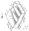
- the rear plate 15 as an electron source substrate and the face plate 17 as an anode substrate are sealed in a peripheral edge portion through the frame member 16, thereby forming an airtight container. Since the inside of the airtight container is held in a vacuum of about 10 -4 Pa, the spacer 20 in a rectangular thin plate shape is provided as an atmospheric pressure resistance structure in order to prevent a damage by the atmospheric pressure, sudden shock, or the like. In a region out of an image display region, an edge portion of the spacer 20 is fixed by the fixing member 25.
- the charging phenomenon of the surface of the spacer 20 having the rough surface relates to the penetration length (dp) of the primary electron which penetrates into the spacer and the thickness of high resistance film 32 formed on the spacer surface.
- n 1
- n > 1 the number of generated electrons per unit depth has distribution for the depth.
- a maximum value of the n value on the definition is equal to 2 and, in this instance, the energy deactivating mode at the time of collision of the medium and the electron is an elastic scattering mode.
- the secondary electron emission coefficient ( ⁇ ) is measured by using a general scanning electron microscope (SEM) equipped with an electron ammeter.
- the primary electron current is measured by using an ammeter equipped with a Faraday cup collector.
- the emission secondary electron current amount is measured by using an ammeter equipped with a collector (an MCP or the like can be also used) as a detector.
- the secondary electron emission coefficient ( ⁇ ) may be also obtained from a sample current and the primary electron current by using a relation of a continuity rule of the sample current passing through a sample portion, the primary electron current, and the emission secondary electron current.
- a film whose specific gravity is higher than that of the high resistance film 1 is used as a high resistance film 2.
- a process tact can be raised without setting the necessary film thickness of high resistance film 2 to an excessive thick value by suppressing the effective electron penetration length, and a film peel-off or the like can be suppressed by suppressing the residual stress of the film on the insulating substrate due to the thick film thickness.
Landscapes
- Physics & Mathematics (AREA)
- General Physics & Mathematics (AREA)
- Cathode-Ray Tubes And Fluorescent Screens For Display (AREA)
- Vessels, Lead-In Wires, Accessory Apparatuses For Cathode-Ray Tubes (AREA)
Applications Claiming Priority (1)
| Application Number | Priority Date | Filing Date | Title |
|---|---|---|---|
| JP2004356502 | 2004-12-09 |
Publications (3)
| Publication Number | Publication Date |
|---|---|
| EP1670026A2 true EP1670026A2 (de) | 2006-06-14 |
| EP1670026A3 EP1670026A3 (de) | 2008-05-28 |
| EP1670026B1 EP1670026B1 (de) | 2011-05-04 |
Family
ID=36061200
Family Applications (1)
| Application Number | Title | Priority Date | Filing Date |
|---|---|---|---|
| EP05026405A Expired - Lifetime EP1670026B1 (de) | 2004-12-09 | 2005-12-02 | Bilderzeugungsgerät |
Country Status (5)
| Country | Link |
|---|---|
| US (1) | US7449827B2 (de) |
| EP (1) | EP1670026B1 (de) |
| KR (1) | KR100845905B1 (de) |
| CN (1) | CN1787163B (de) |
| DE (1) | DE602005027798D1 (de) |
Families Citing this family (5)
| Publication number | Priority date | Publication date | Assignee | Title |
|---|---|---|---|---|
| JP2008010399A (ja) * | 2006-05-31 | 2008-01-17 | Canon Inc | 画像表示装置 |
| EP2064924A4 (de) * | 2006-06-28 | 2009-09-09 | Thomson Licensing | Beschichtung für abstandselemente in emissionsdisplays |
| JP2008016254A (ja) * | 2006-07-04 | 2008-01-24 | Hitachi Ltd | 平面型画像表示装置およびスペーサ |
| JP2008293960A (ja) * | 2007-04-23 | 2008-12-04 | Canon Inc | 導電性部材とこれを用いたスペーサ、及び画像表示装置 |
| KR102847371B1 (ko) * | 2018-12-26 | 2025-08-14 | 엘지디스플레이 주식회사 | 발광 표시 장치 |
Citations (1)
| Publication number | Priority date | Publication date | Assignee | Title |
|---|---|---|---|---|
| US20030141803A1 (en) | 2002-01-30 | 2003-07-31 | Masahiro Fushimi | Image-forming apparatus and spacer |
Family Cites Families (4)
| Publication number | Priority date | Publication date | Assignee | Title |
|---|---|---|---|---|
| WO1996018204A1 (en) * | 1994-12-05 | 1996-06-13 | Color Planar Displays, Inc. | Support structure for flat panel displays |
| EP1115137A1 (de) * | 1996-12-26 | 2001-07-11 | Canon Kabushiki Kaisha | Abstandshalter, Bilderzeugungsgerät und Herstellungsverfahren dafür |
| JP4115051B2 (ja) * | 1998-10-07 | 2008-07-09 | キヤノン株式会社 | 電子線装置 |
| KR100396304B1 (ko) * | 1999-02-24 | 2003-09-03 | 캐논 가부시끼가이샤 | 전자선 장치 및 화상 형성 장치 |
-
2005
- 2005-11-29 US US11/288,189 patent/US7449827B2/en not_active Expired - Fee Related
- 2005-12-02 DE DE602005027798T patent/DE602005027798D1/de not_active Expired - Lifetime
- 2005-12-02 EP EP05026405A patent/EP1670026B1/de not_active Expired - Lifetime
- 2005-12-09 CN CN2005100228907A patent/CN1787163B/zh not_active Expired - Fee Related
- 2005-12-09 KR KR1020050120490A patent/KR100845905B1/ko not_active Expired - Fee Related
Patent Citations (1)
| Publication number | Priority date | Publication date | Assignee | Title |
|---|---|---|---|---|
| US20030141803A1 (en) | 2002-01-30 | 2003-07-31 | Masahiro Fushimi | Image-forming apparatus and spacer |
Also Published As
| Publication number | Publication date |
|---|---|
| CN1787163A (zh) | 2006-06-14 |
| EP1670026B1 (de) | 2011-05-04 |
| CN1787163B (zh) | 2010-11-17 |
| DE602005027798D1 (de) | 2011-06-16 |
| US20060125374A1 (en) | 2006-06-15 |
| KR100845905B1 (ko) | 2008-07-11 |
| EP1670026A3 (de) | 2008-05-28 |
| US7449827B2 (en) | 2008-11-11 |
| KR20060065555A (ko) | 2006-06-14 |
Similar Documents
| Publication | Publication Date | Title |
|---|---|---|
| JP3905925B2 (ja) | フラットパネルディスプレイにおける画素情報の表示方法 | |
| EP0810626A2 (de) | Beschichtete Abstandsstruktur für eine Feldemissionsanzeigevorrichtung | |
| CN101454862B (zh) | 图像显示装置 | |
| KR20070060056A (ko) | 화상형성장치 | |
| US6600263B1 (en) | Electron beam apparatus and image forming apparatus | |
| JP2008010399A5 (de) | ||
| US6218783B1 (en) | High voltage compatible spacer coating | |
| EP1670026B1 (de) | Bilderzeugungsgerät | |
| US6963159B2 (en) | Image-forming apparatus and spacer | |
| EP1507280A1 (de) | Bildanzeigevorrichtung | |
| EP0392615B1 (de) | Farbbildröhre und Bildwiedergabeanordnung mit einer derartigen Bildröhre | |
| JP5037817B2 (ja) | 画像形成装置 | |
| US7548017B2 (en) | Surface conduction electron emitter display | |
| US20060284545A1 (en) | Image display device | |
| US20080174234A1 (en) | Display device and spacer for display device | |
| JP2010182697A (ja) | 画像表示装置 | |
| JP2004079359A (ja) | 電子線装置およびそのスペーサ | |
| JP2009009929A (ja) | 画像表示装置 | |
| US20110019345A1 (en) | Image display apparatus | |
| JPH04206235A (ja) | ガス放電パネル | |
| JP2008159549A (ja) | 画像表示装置 | |
| HK1084231A (en) | Flat panel display with high voltage spacer |
Legal Events
| Date | Code | Title | Description |
|---|---|---|---|
| PUAI | Public reference made under article 153(3) epc to a published international application that has entered the european phase |
Free format text: ORIGINAL CODE: 0009012 |
|
| AK | Designated contracting states |
Kind code of ref document: A2 Designated state(s): AT BE BG CH CY CZ DE DK EE ES FI FR GB GR HU IE IS IT LI LT LU LV MC NL PL PT RO SE SI SK TR |
|
| AX | Request for extension of the european patent |
Extension state: AL BA HR MK YU |
|
| PUAL | Search report despatched |
Free format text: ORIGINAL CODE: 0009013 |
|
| AK | Designated contracting states |
Kind code of ref document: A3 Designated state(s): AT BE BG CH CY CZ DE DK EE ES FI FR GB GR HU IE IS IT LI LT LU LV MC NL PL PT RO SE SI SK TR |
|
| AX | Request for extension of the european patent |
Extension state: AL BA HR MK YU |
|
| 17P | Request for examination filed |
Effective date: 20081128 |
|
| AKX | Designation fees paid |
Designated state(s): DE FR GB IT NL |
|
| 17Q | First examination report despatched |
Effective date: 20090119 |
|
| GRAP | Despatch of communication of intention to grant a patent |
Free format text: ORIGINAL CODE: EPIDOSNIGR1 |
|
| GRAS | Grant fee paid |
Free format text: ORIGINAL CODE: EPIDOSNIGR3 |
|
| GRAA | (expected) grant |
Free format text: ORIGINAL CODE: 0009210 |
|
| AK | Designated contracting states |
Kind code of ref document: B1 Designated state(s): DE FR GB IT NL |
|
| REG | Reference to a national code |
Ref country code: GB Ref legal event code: FG4D |
|
| REF | Corresponds to: |
Ref document number: 602005027798 Country of ref document: DE Date of ref document: 20110616 Kind code of ref document: P |
|
| REG | Reference to a national code |
Ref country code: DE Ref legal event code: R096 Ref document number: 602005027798 Country of ref document: DE Effective date: 20110616 |
|
| REG | Reference to a national code |
Ref country code: NL Ref legal event code: VDEP Effective date: 20110504 |
|
| PG25 | Lapsed in a contracting state [announced via postgrant information from national office to epo] |
Ref country code: NL Free format text: LAPSE BECAUSE OF FAILURE TO SUBMIT A TRANSLATION OF THE DESCRIPTION OR TO PAY THE FEE WITHIN THE PRESCRIBED TIME-LIMIT Effective date: 20110504 |
|
| PLBE | No opposition filed within time limit |
Free format text: ORIGINAL CODE: 0009261 |
|
| STAA | Information on the status of an ep patent application or granted ep patent |
Free format text: STATUS: NO OPPOSITION FILED WITHIN TIME LIMIT |
|
| 26N | No opposition filed |
Effective date: 20120207 |
|
| PG25 | Lapsed in a contracting state [announced via postgrant information from national office to epo] |
Ref country code: IT Free format text: LAPSE BECAUSE OF FAILURE TO SUBMIT A TRANSLATION OF THE DESCRIPTION OR TO PAY THE FEE WITHIN THE PRESCRIBED TIME-LIMIT Effective date: 20110504 |
|
| REG | Reference to a national code |
Ref country code: DE Ref legal event code: R097 Ref document number: 602005027798 Country of ref document: DE Effective date: 20120207 |
|
| GBPC | Gb: european patent ceased through non-payment of renewal fee |
Effective date: 20111202 |
|
| REG | Reference to a national code |
Ref country code: FR Ref legal event code: ST Effective date: 20120831 |
|
| PG25 | Lapsed in a contracting state [announced via postgrant information from national office to epo] |
Ref country code: GB Free format text: LAPSE BECAUSE OF NON-PAYMENT OF DUE FEES Effective date: 20111202 |
|
| PG25 | Lapsed in a contracting state [announced via postgrant information from national office to epo] |
Ref country code: FR Free format text: LAPSE BECAUSE OF NON-PAYMENT OF DUE FEES Effective date: 20120102 |
|
| PGFP | Annual fee paid to national office [announced via postgrant information from national office to epo] |
Ref country code: DE Payment date: 20121231 Year of fee payment: 8 |
|
| REG | Reference to a national code |
Ref country code: DE Ref legal event code: R119 Ref document number: 602005027798 Country of ref document: DE |
|
| REG | Reference to a national code |
Ref country code: DE Ref legal event code: R119 Ref document number: 602005027798 Country of ref document: DE Effective date: 20140701 |
|
| PG25 | Lapsed in a contracting state [announced via postgrant information from national office to epo] |
Ref country code: DE Free format text: LAPSE BECAUSE OF NON-PAYMENT OF DUE FEES Effective date: 20140701 |