EP1665469B1 - Interconnect system - Google Patents
Interconnect system Download PDFInfo
- Publication number
- EP1665469B1 EP1665469B1 EP04779460A EP04779460A EP1665469B1 EP 1665469 B1 EP1665469 B1 EP 1665469B1 EP 04779460 A EP04779460 A EP 04779460A EP 04779460 A EP04779460 A EP 04779460A EP 1665469 B1 EP1665469 B1 EP 1665469B1
- Authority
- EP
- European Patent Office
- Prior art keywords
- circuit board
- printed circuit
- header connector
- header
- conductive
- Prior art date
- Legal status (The legal status is an assumption and is not a legal conclusion. Google has not performed a legal analysis and makes no representation as to the accuracy of the status listed.)
- Expired - Lifetime
Links
- 238000003780 insertion Methods 0.000 claims description 8
- 230000037431 insertion Effects 0.000 claims description 8
- 238000000034 method Methods 0.000 claims description 6
- 230000013011 mating Effects 0.000 abstract description 3
- 238000005516 engineering process Methods 0.000 abstract description 2
- 230000005540 biological transmission Effects 0.000 description 2
- 229910000881 Cu alloy Inorganic materials 0.000 description 1
- 229920000106 Liquid crystal polymer Polymers 0.000 description 1
- 239000004977 Liquid-crystal polymers (LCPs) Substances 0.000 description 1
- 238000004891 communication Methods 0.000 description 1
- 238000004519 manufacturing process Methods 0.000 description 1
- 239000012815 thermoplastic material Substances 0.000 description 1
Images

Classifications
-
- H—ELECTRICITY
- H01—ELECTRIC ELEMENTS
- H01R—ELECTRICALLY-CONDUCTIVE CONNECTIONS; STRUCTURAL ASSOCIATIONS OF A PLURALITY OF MUTUALLY-INSULATED ELECTRICAL CONNECTING ELEMENTS; COUPLING DEVICES; CURRENT COLLECTORS
- H01R12/00—Structural associations of a plurality of mutually-insulated electrical connecting elements, specially adapted for printed circuits, e.g. printed circuit boards [PCB], flat or ribbon cables, or like generally planar structures, e.g. terminal strips, terminal blocks; Coupling devices specially adapted for printed circuits, flat or ribbon cables, or like generally planar structures; Terminals specially adapted for contact with, or insertion into, printed circuits, flat or ribbon cables, or like generally planar structures
- H01R12/70—Coupling devices
- H01R12/71—Coupling devices for rigid printing circuits or like structures
-
- H—ELECTRICITY
- H01—ELECTRIC ELEMENTS
- H01R—ELECTRICALLY-CONDUCTIVE CONNECTIONS; STRUCTURAL ASSOCIATIONS OF A PLURALITY OF MUTUALLY-INSULATED ELECTRICAL CONNECTING ELEMENTS; COUPLING DEVICES; CURRENT COLLECTORS
- H01R12/00—Structural associations of a plurality of mutually-insulated electrical connecting elements, specially adapted for printed circuits, e.g. printed circuit boards [PCB], flat or ribbon cables, or like generally planar structures, e.g. terminal strips, terminal blocks; Coupling devices specially adapted for printed circuits, flat or ribbon cables, or like generally planar structures; Terminals specially adapted for contact with, or insertion into, printed circuits, flat or ribbon cables, or like generally planar structures
- H01R12/70—Coupling devices
- H01R12/71—Coupling devices for rigid printing circuits or like structures
- H01R12/712—Coupling devices for rigid printing circuits or like structures co-operating with the surface of the printed circuit or with a coupling device exclusively provided on the surface of the printed circuit
- H01R12/714—Coupling devices for rigid printing circuits or like structures co-operating with the surface of the printed circuit or with a coupling device exclusively provided on the surface of the printed circuit with contacts abutting directly the printed circuit; Button contacts therefore provided on the printed circuit
-
- H—ELECTRICITY
- H01—ELECTRIC ELEMENTS
- H01R—ELECTRICALLY-CONDUCTIVE CONNECTIONS; STRUCTURAL ASSOCIATIONS OF A PLURALITY OF MUTUALLY-INSULATED ELECTRICAL CONNECTING ELEMENTS; COUPLING DEVICES; CURRENT COLLECTORS
- H01R13/00—Details of coupling devices of the kinds covered by groups H01R12/70 or H01R24/00 - H01R33/00
- H01R13/648—Protective earth or shield arrangements on coupling devices, e.g. anti-static shielding
- H01R13/658—High frequency shielding arrangements, e.g. against EMI [Electro-Magnetic Interference] or EMP [Electro-Magnetic Pulse]
- H01R13/6581—Shield structure
- H01R13/6585—Shielding material individually surrounding or interposed between mutually spaced contacts
-
- H—ELECTRICITY
- H01—ELECTRIC ELEMENTS
- H01R—ELECTRICALLY-CONDUCTIVE CONNECTIONS; STRUCTURAL ASSOCIATIONS OF A PLURALITY OF MUTUALLY-INSULATED ELECTRICAL CONNECTING ELEMENTS; COUPLING DEVICES; CURRENT COLLECTORS
- H01R43/00—Apparatus or processes specially adapted for manufacturing, assembling, maintaining, or repairing of line connectors or current collectors or for joining electric conductors
- H01R43/20—Apparatus or processes specially adapted for manufacturing, assembling, maintaining, or repairing of line connectors or current collectors or for joining electric conductors for assembling or disassembling contact members with insulating base, case or sleeve
-
- H—ELECTRICITY
- H01—ELECTRIC ELEMENTS
- H01R—ELECTRICALLY-CONDUCTIVE CONNECTIONS; STRUCTURAL ASSOCIATIONS OF A PLURALITY OF MUTUALLY-INSULATED ELECTRICAL CONNECTING ELEMENTS; COUPLING DEVICES; CURRENT COLLECTORS
- H01R43/00—Apparatus or processes specially adapted for manufacturing, assembling, maintaining, or repairing of line connectors or current collectors or for joining electric conductors
- H01R43/20—Apparatus or processes specially adapted for manufacturing, assembling, maintaining, or repairing of line connectors or current collectors or for joining electric conductors for assembling or disassembling contact members with insulating base, case or sleeve
- H01R43/205—Apparatus or processes specially adapted for manufacturing, assembling, maintaining, or repairing of line connectors or current collectors or for joining electric conductors for assembling or disassembling contact members with insulating base, case or sleeve with a panel or printed circuit board
Definitions
- the present invention relates to an electrical interconnect system.
- the present invention relates to a header connector design that exhibits self-leveling when assembled to a printed circuit board.
- two-part electronic backplane connectors are used to couple a motherboard (also known as a "backplane") to a daughtercard.
- a motherboard also known as a "backplane”
- a socket connector is assembled to the daughtercard while a header connector is assembled to the motherboard.
- a header connector for an interconnect system is known e.g. from US 2001/0012730 A1 .
- This known header connector comprises a header body having a front wall which includes a plurality of first and second passage ways disposed between an internal surface and an external surface.
- a plurality of conductive pins is provided configured for inserting into the first passage ways wherein each conductive pin has a first end extending from the internal surface and an intermediate section disposed in the first passage way.
- the known header body comprises a plurality of shield blades configured for insertion into the second passage ways, wherein each shield blade has a first end extending from the internal surface, an intermediate section disposed in the second passage way, and a second end extending from the external surface of the front wall.
- the present invention provides an interconnect system of claim 1 and a method of assembling an interconnect system of claim 7.
- interconnect systems that use surface mount technology for mating conductive pins in a header connector to surface mount pads on a printed circuit board.
- the printed circuit board may and usually does contain other components to mate with the header connector.
- the present invention discloses in detail a header connector for use with a printed circuit board, one skilled in the art will appreciate that the invention can be used in other electronic interconnect systems where self-leveling of the electronic component is desired.
- each conductive pin of the header connector moves, in rotation to the front wall of the header body, longitudinally in the first passageway.
- the conductive pin moves and makes contact with the surface mount pads.
- a few first conductive pins may make contact with the surface mount pads while others may not yet have made contact.
- the distance between the truncated end of these first contact conductive pins will shorten as other conductive pins (those that still have to be mated) make contact with the surface mount pads.
- the second end of the shield blades of the header connector mate with the plated through holes (commonly referred to as conductive vias) in the printed circuit board.
- conductive vias plated through holes
- the conductive pins move "longitudinally" it is meant that the pins move in a direction perpendicular to the front wall of the header body and thus normal to the printed circuit board, as the front wall of the header body usually lies substantially parallel to the printed circuit board. In other words, the conductive pins move along its length during the assembly to the printed circuit board.
- the term "truncated" as used to describe the conductive pin, means that one end of the conductive pin, typically the end that will eventually make contact with the surface mount pads of the printed circuit board, is not in the form of an apex but instead is replaced by a substantially planar section. Furthermore, the second end of the conductive pin does not contain a spring like element.
- the statement that the "conductive pins are not fully inserted into the first opening” means that the conductive pins remain substantially stationary while residing in the header body but during assembly of the header connector to the printed circuit board, the conductive pins will move longitudinally with respect to the front wall of the header body.
- the conductive pins stop moving when the header connector is fully assembled to the printed circuit board, i.e., when substantially all of the pins have mated with the surface mount pads.
- An advantage of the present invention is that because the conductive pins are not fully inserted into the first passageways of the header body, the pins are free to move with respect to the front wall of the header body when the header connector is assembled to a printed circuit board.
- This feature allows the plurality of conductive pins to exhibit self-leveling, i.e., each pin can adjust its height, with respect to the front wall of the header body, so that the header connector as a whole will have intimate mechanical, and thus electrical contact between the pin and the surface mount pad.
- header connector that allows for self-leveling is an advantageous feature because it reduces the need to have tight mechanical tolerances on the header connector as well as the printed circuit board.
- An advantage of another exemplary embodiment of the present invention is that because the cross-sectional area of the conductive pin is similar to the surface area of the surface mount pad (each pad preferably containing a conductive path into the printed circuit board), minimal discontinuities are present through the entire electrical communication channel thus minimizing the amount of impedance variance present in the system. As a result, the inventive interconnect system exhibits high electrical performance.
- Yet another advantage of another exemplary embodiment is that because the conductive pins are designed to self-level and to contact surface mount pads on the printed circuit board, the insertion force required to assemble a header connector to a printed circuit board can be lower, as compared to an interconnect system using a header connector where both the conductive pins and the shield blades are inserted into plated through hole conductive vias on a printed circuit board.
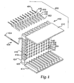
- Figure 1 is an exploded perspective view of one exemplary header connector showing a truncated conductive pin, a continuous strip of shield blades, and a header body; wherein remaining pins and strips of shield blades have been omitted for illustrative purposes; and
- Figure 2 is a perspective view of the header connector of Figure 1;
- Figure 3 is a cross-sectional view an interconnect system where the header connector of Figure 1 has been assembled to one exemplary printed circuit board.
- Figure 1 shows an exploded view of one exemplary header connector 400 having header body 402, one of a plurality of truncated conductive pins 404, and continuous strip 428 having a plurality of shield blades formed therein.
- the header body includes vertical front wall 410, having external surface 424 and internal surface 422, and top and bottom laterally extending horizontal walls 412 and 414 projecting from the front wall.
- the front wall further includes a plurality of first passages 416 for receiving the conductive pins and a plurality of second passages 418 for receiving the shield blades, the passages extending between internal and external surfaces 422 and 424 respectively.
- the header body is typically molded from suitable thermoplastic materials, such as liquid crystal polymers.
- the conductive pins and continuous strip of shield blades are typically plated copper alloys.
- One skilled in the connector art will readily understand that method of making the header body, the conductive pins and the continuous strip of shield blades are known in the art.
- Figure 1 shows a continuous strip of shield blades, it is within the scope of the present invention to use individual shield blades if desired.
- each conductive pin has a first end 452 that extends above external wall 422, truncated second end 454 spaced apart from first end 452 and configured for contacting a surface mount pad on a printed circuit board (not shown), and an intermediate portion disposed between the first end and the second end. In use, the intermediate portion lies in the first passages.
- the shield blades are formed to include generally right angle shielding leg portions (denoted collectively as 430 and 432) configured for insertion into the second passages 418.
- Each shield blade includes first end 462 that extends above internal surface 422 of the vertical front wall of the header body. In use, first end 462 of the shield blade lies generally adjacent to and substantially parallel to first end 452 of the conductive pin.
- Second end 464 of the shield blade is spaced apart from first end 462 and is configured for insertion into a plated through hole in the printed circuit board (not shown).
- Each shield blade also includes shield tail 448, which provides a friction fit to the printed circuit board once inserted therein, and is substantially perpendicular to first and second leg portions 430 and 432 respectively.
- first passages 416 and second passages 418 are arranged symmetrically in front wall 410 of header body 402 such that generally right angle shielding portions of shield blade substantially surround conductive pins 404 to form a coaxial shield around the conductive pins.
- Each second passage 418 includes a central portion 434 coupled to first and second end portions 436 and 438 respectively by first and second narrowed throat portions 440 and 442 respectively.
- the first and second narrowed throat portions are dimensioned to frictionally engage first and second leg portions of the shield blades to hold them in place in the header body. That is to say, the shield blades are fully inserted into the header body in second passages 418.
- header connector 400 when header connector 400 is assembled to the printed circuit board, the shield blades remain stationary with respect to the header body.
- conductive pins 404 are not fully inserted into first openings 416 so that as the header connector is assembled to the printed circuit board, the conductive pin can move longitudinally to make contact with the surface mount pad on the printed circuit board. This ability for the conductive pins to move or to float during assembly allows the header connector to self-level, among other advantages.
- Figure 2 shows a perspective view of the header connector of Figure 1 where the conductive pins and shield blades have been installed.
- the conductive pins are short seated into the header body such that second end 454 extends above front wall 410 by some predetermined height.
- the truncated end of the conductive pin extends about 0.020 inch (0.51 mm) above the external surface of front wall 410 of the header body.
- the conductive pins that extend from the external surface of the header body form an array of conductive pins.
- header connector embodied in Figure 1 represents only one type of header connector that can be used in the present invention.
- any header connector that contains a plurality of conductive pins that have a truncated end and a plurality of shield blades can be used in the present invention.
- Figure 3 shows a cross sectional view of the header connector of Figure 1 assembled on printed circuit board 34.
- second end 454 of each conductive pin 404 is in direct contact with surface mount pad 36 of the printed circuit board and second end 464 of the shield blades mate with the plated through holes 38 in the printed circuit board.
- the conductive pins are also designed to be substantially straight with a substantially constant cross section.
- the conductive pin does not contain and does not rely on a spring element at its second end to made mechanical contact with the surface mount pads. The combination of these features results in minimizing the impedance variance of the electrical signal to yield a higher performing, i.e., faster data transmission, interconnects.
- header connector When the header connector is used with a printed circuit board to yield an interconnect device, there are means to hold the header connector the board.
- frictional forces between the shield tail and the pleated through holes hold the header connector to the printed circuit board while also maintaining the conductive pins in their contact positions to the surface mount pads.
- mechanical means including but not limited to screws or clamps.
- socket connectors can be used to mate with the header connector.
- An exemplary socket connector and connector modules that can be used with the present invention is disclosed in US Patent Nos. 6,146,202 and 6,231,391 .
Landscapes
- Engineering & Computer Science (AREA)
- Manufacturing & Machinery (AREA)
- Coupling Device And Connection With Printed Circuit (AREA)
- Details Of Connecting Devices For Male And Female Coupling (AREA)
- Small-Scale Networks (AREA)
- Time-Division Multiplex Systems (AREA)
- Mechanical Coupling Of Light Guides (AREA)
- Use Of Switch Circuits For Exchanges And Methods Of Control Of Multiplex Exchanges (AREA)
Applications Claiming Priority (2)
| Application Number | Priority Date | Filing Date | Title |
|---|---|---|---|
| US10/658,019 US7101224B2 (en) | 2003-09-09 | 2003-09-09 | Interconnect system |
| PCT/US2004/024412 WO2005027274A1 (en) | 2003-09-09 | 2004-07-29 | Interconnect system |
Publications (2)
| Publication Number | Publication Date |
|---|---|
| EP1665469A1 EP1665469A1 (en) | 2006-06-07 |
| EP1665469B1 true EP1665469B1 (en) | 2007-09-12 |
Family
ID=34194692
Family Applications (1)
| Application Number | Title | Priority Date | Filing Date |
|---|---|---|---|
| EP04779460A Expired - Lifetime EP1665469B1 (en) | 2003-09-09 | 2004-07-29 | Interconnect system |
Country Status (11)
| Country | Link |
|---|---|
| US (1) | US7101224B2 (cg-RX-API-DMAC7.html) |
| EP (1) | EP1665469B1 (cg-RX-API-DMAC7.html) |
| JP (1) | JP4633056B2 (cg-RX-API-DMAC7.html) |
| KR (1) | KR20060082077A (cg-RX-API-DMAC7.html) |
| CN (2) | CN100541921C (cg-RX-API-DMAC7.html) |
| AT (1) | ATE373326T1 (cg-RX-API-DMAC7.html) |
| DE (1) | DE602004008947T2 (cg-RX-API-DMAC7.html) |
| IL (1) | IL173516A0 (cg-RX-API-DMAC7.html) |
| MY (1) | MY138765A (cg-RX-API-DMAC7.html) |
| TW (1) | TWI336543B (cg-RX-API-DMAC7.html) |
| WO (1) | WO2005027274A1 (cg-RX-API-DMAC7.html) |
Families Citing this family (10)
| Publication number | Priority date | Publication date | Assignee | Title |
|---|---|---|---|---|
| US8136233B2 (en) * | 2003-10-09 | 2012-03-20 | Solectron Corporation | Tools for seating connectors on substrates |
| US7423400B2 (en) * | 2006-06-21 | 2008-09-09 | Flextronics Automotive Inc. | System and method for controlling velocity and detecting obstructions of a vehicle lift gate |
| US7592762B2 (en) * | 2006-06-21 | 2009-09-22 | Flextronics Automotive Inc. | System and method for establishing a reference angle for controlling a vehicle rotational closure system |
| US7586280B2 (en) * | 2006-06-21 | 2009-09-08 | Flextronics Automotive Inc. | System and method for establishing a reference angle for controlling a vehicle rotational closure system |
| CN101459299B (zh) * | 2007-12-11 | 2010-11-17 | 富士康(昆山)电脑接插件有限公司 | 电连接器 |
| TWI483478B (zh) | 2011-03-17 | 2015-05-01 | Molex Inc | Connectors and connector systems |
| US9629256B2 (en) | 2013-11-07 | 2017-04-18 | Flextronics Corporation | Tools for seating connectors on substrates |
| CN105682359A (zh) * | 2016-01-18 | 2016-06-15 | 冯俊谊 | 一种pcb及其表面贴装工艺 |
| CN107658588B (zh) * | 2017-08-22 | 2020-06-09 | 番禺得意精密电子工业有限公司 | 电连接器 |
| WO2022195986A1 (ja) * | 2021-03-17 | 2022-09-22 | イリソ電子工業株式会社 | フローティングコネクタ |
Family Cites Families (8)
| Publication number | Priority date | Publication date | Assignee | Title |
|---|---|---|---|---|
| US4695106A (en) * | 1985-05-13 | 1987-09-22 | Amp Incorporated | Surface mount, miniature connector |
| US4726793A (en) * | 1986-02-06 | 1988-02-23 | Amp Incorporated | Electrical socket, application tool and method for positioning electrical sockets on circuit boards for surface soldering |
| GB8803893D0 (en) | 1988-02-19 | 1988-03-23 | Bicc Plc | Electrical connector |
| US4968263A (en) * | 1990-03-28 | 1990-11-06 | Molex Incorporated | Multi-pin electrical connector with floating terminal pins |
| US5174764A (en) * | 1991-12-20 | 1992-12-29 | Amp Incorporated | Connector assembly having surface mounted terminals |
| US5755596A (en) | 1996-11-19 | 1998-05-26 | Watson; Troy M. | High-density compression connector |
| US6231391B1 (en) * | 1999-08-12 | 2001-05-15 | Robinson Nugent, Inc. | Connector apparatus |
| DE69929613T2 (de) | 1998-08-12 | 2006-09-28 | Robinson Nugent, Inc., New Albany | Verbindungsvorrichtung |
-
2003
- 2003-09-09 US US10/658,019 patent/US7101224B2/en not_active Expired - Fee Related
-
2004
- 2004-07-29 KR KR1020067004747A patent/KR20060082077A/ko not_active Abandoned
- 2004-07-29 CN CNB2004800259504A patent/CN100541921C/zh not_active Expired - Fee Related
- 2004-07-29 WO PCT/US2004/024412 patent/WO2005027274A1/en not_active Ceased
- 2004-07-29 EP EP04779460A patent/EP1665469B1/en not_active Expired - Lifetime
- 2004-07-29 CN CN200910133517A patent/CN101540447A/zh active Pending
- 2004-07-29 JP JP2006525332A patent/JP4633056B2/ja not_active Expired - Fee Related
- 2004-07-29 AT AT04779460T patent/ATE373326T1/de not_active IP Right Cessation
- 2004-07-29 DE DE602004008947T patent/DE602004008947T2/de not_active Expired - Lifetime
- 2004-08-13 TW TW093124445A patent/TWI336543B/zh not_active IP Right Cessation
- 2004-08-19 MY MYPI20043392A patent/MY138765A/en unknown
-
2006
- 2006-02-02 IL IL173516A patent/IL173516A0/en unknown
Non-Patent Citations (1)
| Title |
|---|
| None * |
Also Published As
| Publication number | Publication date |
|---|---|
| WO2005027274A1 (en) | 2005-03-24 |
| MY138765A (en) | 2009-07-31 |
| EP1665469A1 (en) | 2006-06-07 |
| DE602004008947T2 (de) | 2008-05-15 |
| TW200524222A (en) | 2005-07-16 |
| US20050042925A1 (en) | 2005-02-24 |
| KR20060082077A (ko) | 2006-07-14 |
| JP2007505449A (ja) | 2007-03-08 |
| ATE373326T1 (de) | 2007-09-15 |
| US7101224B2 (en) | 2006-09-05 |
| CN1849728A (zh) | 2006-10-18 |
| DE602004008947D1 (de) | 2007-10-25 |
| CN100541921C (zh) | 2009-09-16 |
| TWI336543B (en) | 2011-01-21 |
| CN101540447A (zh) | 2009-09-23 |
| IL173516A0 (en) | 2006-07-05 |
| JP4633056B2 (ja) | 2011-02-16 |
Similar Documents
| Publication | Publication Date | Title |
|---|---|---|
| US12531363B2 (en) | Connector assembly | |
| JP3135005B2 (ja) | 電気コネクタ | |
| US9608383B2 (en) | High density electrical connector with shield plate louvers | |
| US7997938B2 (en) | Electrical connector system with electrical power connection and guide features | |
| US7883366B2 (en) | High density connector assembly | |
| US7985097B2 (en) | Electrical connector assembly | |
| US10553971B1 (en) | Card edge connector having a contact positioner | |
| US20050101188A1 (en) | High-speed electrical connector | |
| CN103563179B (zh) | 连接器及连接器系统 | |
| JPH04229574A (ja) | コネクタアセンブリ | |
| US6866518B1 (en) | Electrical interconnection between multiple printed circuit boards | |
| US10923856B2 (en) | Polarization feature for a receptacle cage | |
| US6918775B2 (en) | Method for interconnecting multiple printed circuit boards | |
| US7736183B2 (en) | Connector assembly with variable stack heights having power and signal contacts | |
| CN1398446A (zh) | 带屏蔽的连接器 | |
| JPH04229573A (ja) | 接地構造を有するコネクタ | |
| EP1964214A1 (en) | Boardmount header to cable connector assembly | |
| CN101828311B (zh) | 电连接器组件 | |
| US20240235116A1 (en) | Circuit board assembly for a communication system | |
| US10468798B2 (en) | Electrical contact pre-load structure | |
| US20060030221A1 (en) | Modular jack connector having improved performance | |
| US7101224B2 (en) | Interconnect system | |
| CN114583482B (zh) | 电连接器组件 | |
| CN103842867A (zh) | 电触点和电连接器 | |
| US5938456A (en) | Low profile electrical connector |
Legal Events
| Date | Code | Title | Description |
|---|---|---|---|
| PUAI | Public reference made under article 153(3) epc to a published international application that has entered the european phase |
Free format text: ORIGINAL CODE: 0009012 |
|
| 17P | Request for examination filed |
Effective date: 20060306 |
|
| AK | Designated contracting states |
Kind code of ref document: A1 Designated state(s): AT BE BG CH CY CZ DE DK EE ES FI FR GB GR HU IE IT LI LU MC NL PL PT RO SE SI SK TR |
|
| 17Q | First examination report despatched |
Effective date: 20060707 |
|
| DAX | Request for extension of the european patent (deleted) | ||
| GRAP | Despatch of communication of intention to grant a patent |
Free format text: ORIGINAL CODE: EPIDOSNIGR1 |
|
| GRAS | Grant fee paid |
Free format text: ORIGINAL CODE: EPIDOSNIGR3 |
|
| GRAA | (expected) grant |
Free format text: ORIGINAL CODE: 0009210 |
|
| AK | Designated contracting states |
Kind code of ref document: B1 Designated state(s): AT BE BG CH CY CZ DE DK EE ES FI FR GB GR HU IE IT LI LU MC NL PL PT RO SE SI SK TR |
|
| REG | Reference to a national code |
Ref country code: GB Ref legal event code: FG4D |
|
| REG | Reference to a national code |
Ref country code: CH Ref legal event code: EP |
|
| REF | Corresponds to: |
Ref document number: 602004008947 Country of ref document: DE Date of ref document: 20071025 Kind code of ref document: P |
|
| REG | Reference to a national code |
Ref country code: IE Ref legal event code: FG4D |
|
| PG25 | Lapsed in a contracting state [announced via postgrant information from national office to epo] |
Ref country code: FI Free format text: LAPSE BECAUSE OF FAILURE TO SUBMIT A TRANSLATION OF THE DESCRIPTION OR TO PAY THE FEE WITHIN THE PRESCRIBED TIME-LIMIT Effective date: 20070912 |
|
| PG25 | Lapsed in a contracting state [announced via postgrant information from national office to epo] |
Ref country code: AT Free format text: LAPSE BECAUSE OF FAILURE TO SUBMIT A TRANSLATION OF THE DESCRIPTION OR TO PAY THE FEE WITHIN THE PRESCRIBED TIME-LIMIT Effective date: 20070912 Ref country code: CH Free format text: LAPSE BECAUSE OF FAILURE TO SUBMIT A TRANSLATION OF THE DESCRIPTION OR TO PAY THE FEE WITHIN THE PRESCRIBED TIME-LIMIT Effective date: 20070912 Ref country code: LI Free format text: LAPSE BECAUSE OF FAILURE TO SUBMIT A TRANSLATION OF THE DESCRIPTION OR TO PAY THE FEE WITHIN THE PRESCRIBED TIME-LIMIT Effective date: 20070912 Ref country code: PL Free format text: LAPSE BECAUSE OF FAILURE TO SUBMIT A TRANSLATION OF THE DESCRIPTION OR TO PAY THE FEE WITHIN THE PRESCRIBED TIME-LIMIT Effective date: 20070912 |
|
| NLV1 | Nl: lapsed or annulled due to failure to fulfill the requirements of art. 29p and 29m of the patents act | ||
| PG25 | Lapsed in a contracting state [announced via postgrant information from national office to epo] |
Ref country code: BE Free format text: LAPSE BECAUSE OF FAILURE TO SUBMIT A TRANSLATION OF THE DESCRIPTION OR TO PAY THE FEE WITHIN THE PRESCRIBED TIME-LIMIT Effective date: 20070912 |
|
| REG | Reference to a national code |
Ref country code: CH Ref legal event code: PL |
|
| PG25 | Lapsed in a contracting state [announced via postgrant information from national office to epo] |
Ref country code: ES Free format text: LAPSE BECAUSE OF FAILURE TO SUBMIT A TRANSLATION OF THE DESCRIPTION OR TO PAY THE FEE WITHIN THE PRESCRIBED TIME-LIMIT Effective date: 20071223 Ref country code: GR Free format text: LAPSE BECAUSE OF FAILURE TO SUBMIT A TRANSLATION OF THE DESCRIPTION OR TO PAY THE FEE WITHIN THE PRESCRIBED TIME-LIMIT Effective date: 20071213 Ref country code: NL Free format text: LAPSE BECAUSE OF FAILURE TO SUBMIT A TRANSLATION OF THE DESCRIPTION OR TO PAY THE FEE WITHIN THE PRESCRIBED TIME-LIMIT Effective date: 20070912 |
|
| ET | Fr: translation filed | ||
| PG25 | Lapsed in a contracting state [announced via postgrant information from national office to epo] |
Ref country code: PT Free format text: LAPSE BECAUSE OF FAILURE TO SUBMIT A TRANSLATION OF THE DESCRIPTION OR TO PAY THE FEE WITHIN THE PRESCRIBED TIME-LIMIT Effective date: 20080212 Ref country code: SK Free format text: LAPSE BECAUSE OF FAILURE TO SUBMIT A TRANSLATION OF THE DESCRIPTION OR TO PAY THE FEE WITHIN THE PRESCRIBED TIME-LIMIT Effective date: 20070912 Ref country code: CZ Free format text: LAPSE BECAUSE OF FAILURE TO SUBMIT A TRANSLATION OF THE DESCRIPTION OR TO PAY THE FEE WITHIN THE PRESCRIBED TIME-LIMIT Effective date: 20070912 |
|
| PG25 | Lapsed in a contracting state [announced via postgrant information from national office to epo] |
Ref country code: SE Free format text: LAPSE BECAUSE OF FAILURE TO SUBMIT A TRANSLATION OF THE DESCRIPTION OR TO PAY THE FEE WITHIN THE PRESCRIBED TIME-LIMIT Effective date: 20071212 Ref country code: RO Free format text: LAPSE BECAUSE OF FAILURE TO SUBMIT A TRANSLATION OF THE DESCRIPTION OR TO PAY THE FEE WITHIN THE PRESCRIBED TIME-LIMIT Effective date: 20070912 |
|
| PLBE | No opposition filed within time limit |
Free format text: ORIGINAL CODE: 0009261 |
|
| STAA | Information on the status of an ep patent application or granted ep patent |
Free format text: STATUS: NO OPPOSITION FILED WITHIN TIME LIMIT |
|
| PG25 | Lapsed in a contracting state [announced via postgrant information from national office to epo] |
Ref country code: DK Free format text: LAPSE BECAUSE OF FAILURE TO SUBMIT A TRANSLATION OF THE DESCRIPTION OR TO PAY THE FEE WITHIN THE PRESCRIBED TIME-LIMIT Effective date: 20070912 |
|
| 26N | No opposition filed |
Effective date: 20080613 |
|
| PGFP | Annual fee paid to national office [announced via postgrant information from national office to epo] |
Ref country code: IT Payment date: 20080724 Year of fee payment: 5 |
|
| PGFP | Annual fee paid to national office [announced via postgrant information from national office to epo] |
Ref country code: GB Payment date: 20080729 Year of fee payment: 5 |
|
| PG25 | Lapsed in a contracting state [announced via postgrant information from national office to epo] |
Ref country code: MC Free format text: LAPSE BECAUSE OF NON-PAYMENT OF DUE FEES Effective date: 20080731 |
|
| PG25 | Lapsed in a contracting state [announced via postgrant information from national office to epo] |
Ref country code: EE Free format text: LAPSE BECAUSE OF FAILURE TO SUBMIT A TRANSLATION OF THE DESCRIPTION OR TO PAY THE FEE WITHIN THE PRESCRIBED TIME-LIMIT Effective date: 20070912 |
|
| REG | Reference to a national code |
Ref country code: FR Ref legal event code: ST Effective date: 20090331 |
|
| PG25 | Lapsed in a contracting state [announced via postgrant information from national office to epo] |
Ref country code: SI Free format text: LAPSE BECAUSE OF FAILURE TO SUBMIT A TRANSLATION OF THE DESCRIPTION OR TO PAY THE FEE WITHIN THE PRESCRIBED TIME-LIMIT Effective date: 20070912 |
|
| PG25 | Lapsed in a contracting state [announced via postgrant information from national office to epo] |
Ref country code: IE Free format text: LAPSE BECAUSE OF NON-PAYMENT OF DUE FEES Effective date: 20080729 Ref country code: CY Free format text: LAPSE BECAUSE OF FAILURE TO SUBMIT A TRANSLATION OF THE DESCRIPTION OR TO PAY THE FEE WITHIN THE PRESCRIBED TIME-LIMIT Effective date: 20070912 |
|
| PG25 | Lapsed in a contracting state [announced via postgrant information from national office to epo] |
Ref country code: FR Free format text: LAPSE BECAUSE OF NON-PAYMENT OF DUE FEES Effective date: 20080731 Ref country code: BG Free format text: LAPSE BECAUSE OF FAILURE TO SUBMIT A TRANSLATION OF THE DESCRIPTION OR TO PAY THE FEE WITHIN THE PRESCRIBED TIME-LIMIT Effective date: 20071212 |
|
| GBPC | Gb: european patent ceased through non-payment of renewal fee |
Effective date: 20090729 |
|
| PG25 | Lapsed in a contracting state [announced via postgrant information from national office to epo] |
Ref country code: GB Free format text: LAPSE BECAUSE OF NON-PAYMENT OF DUE FEES Effective date: 20090729 |
|
| PG25 | Lapsed in a contracting state [announced via postgrant information from national office to epo] |
Ref country code: LU Free format text: LAPSE BECAUSE OF NON-PAYMENT OF DUE FEES Effective date: 20080729 Ref country code: HU Free format text: LAPSE BECAUSE OF FAILURE TO SUBMIT A TRANSLATION OF THE DESCRIPTION OR TO PAY THE FEE WITHIN THE PRESCRIBED TIME-LIMIT Effective date: 20080313 |
|
| PG25 | Lapsed in a contracting state [announced via postgrant information from national office to epo] |
Ref country code: TR Free format text: LAPSE BECAUSE OF FAILURE TO SUBMIT A TRANSLATION OF THE DESCRIPTION OR TO PAY THE FEE WITHIN THE PRESCRIBED TIME-LIMIT Effective date: 20070912 |
|
| PGFP | Annual fee paid to national office [announced via postgrant information from national office to epo] |
Ref country code: DE Payment date: 20100721 Year of fee payment: 7 |
|
| PG25 | Lapsed in a contracting state [announced via postgrant information from national office to epo] |
Ref country code: IT Free format text: LAPSE BECAUSE OF NON-PAYMENT OF DUE FEES Effective date: 20090729 |
|
| PG25 | Lapsed in a contracting state [announced via postgrant information from national office to epo] |
Ref country code: DE Free format text: LAPSE BECAUSE OF NON-PAYMENT OF DUE FEES Effective date: 20120201 |
|
| REG | Reference to a national code |
Ref country code: DE Ref legal event code: R119 Ref document number: 602004008947 Country of ref document: DE Effective date: 20120201 |