EP1664897B1 - Non-uniform light valve - Google Patents
Non-uniform light valve Download PDFInfo
- Publication number
- EP1664897B1 EP1664897B1 EP04738017A EP04738017A EP1664897B1 EP 1664897 B1 EP1664897 B1 EP 1664897B1 EP 04738017 A EP04738017 A EP 04738017A EP 04738017 A EP04738017 A EP 04738017A EP 1664897 B1 EP1664897 B1 EP 1664897B1
- Authority
- EP
- European Patent Office
- Prior art keywords
- light valve
- imaging
- elements
- resolution channel
- pattern
- Prior art date
- Legal status (The legal status is an assumption and is not a legal conclusion. Google has not performed a legal analysis and makes no representation as to the accuracy of the status listed.)
- Expired - Lifetime
Links
- 238000003384 imaging method Methods 0.000 claims abstract description 126
- 239000000758 substrate Substances 0.000 claims description 71
- 238000000034 method Methods 0.000 claims description 34
- 230000005855 radiation Effects 0.000 claims description 17
- 229910052581 Si3N4 Inorganic materials 0.000 claims description 4
- HQVNEWCFYHHQES-UHFFFAOYSA-N silicon nitride Chemical compound N12[Si]34N5[Si]62N3[Si]51N64 HQVNEWCFYHHQES-UHFFFAOYSA-N 0.000 claims description 4
- 238000012546 transfer Methods 0.000 claims description 4
- 238000000926 separation method Methods 0.000 claims description 3
- 230000005540 biological transmission Effects 0.000 claims description 2
- 238000010438 heat treatment Methods 0.000 claims description 2
- 230000008878 coupling Effects 0.000 claims 2
- 238000010168 coupling process Methods 0.000 claims 2
- 238000005859 coupling reaction Methods 0.000 claims 2
- 230000008569 process Effects 0.000 description 20
- 238000004519 manufacturing process Methods 0.000 description 13
- 239000011159 matrix material Substances 0.000 description 6
- 241000854350 Enicospilus group Species 0.000 description 5
- 238000005286 illumination Methods 0.000 description 5
- 241000526960 Amaranthus acanthochiton Species 0.000 description 4
- 239000000463 material Substances 0.000 description 4
- 230000003287 optical effect Effects 0.000 description 4
- 230000000694 effects Effects 0.000 description 3
- 241000295146 Gallionellaceae Species 0.000 description 2
- XUIMIQQOPSSXEZ-UHFFFAOYSA-N Silicon Chemical compound [Si] XUIMIQQOPSSXEZ-UHFFFAOYSA-N 0.000 description 2
- 239000003086 colorant Substances 0.000 description 2
- 239000007769 metal material Substances 0.000 description 2
- 239000000203 mixture Substances 0.000 description 2
- 239000004065 semiconductor Substances 0.000 description 2
- 230000035945 sensitivity Effects 0.000 description 2
- 229910052710 silicon Inorganic materials 0.000 description 2
- 239000010703 silicon Substances 0.000 description 2
- 238000001931 thermography Methods 0.000 description 2
- RTAQQCXQSZGOHL-UHFFFAOYSA-N Titanium Chemical compound [Ti] RTAQQCXQSZGOHL-UHFFFAOYSA-N 0.000 description 1
- 230000004075 alteration Effects 0.000 description 1
- XAGFODPZIPBFFR-UHFFFAOYSA-N aluminium Chemical compound [Al] XAGFODPZIPBFFR-UHFFFAOYSA-N 0.000 description 1
- 229910052782 aluminium Inorganic materials 0.000 description 1
- 230000008901 benefit Effects 0.000 description 1
- 230000008859 change Effects 0.000 description 1
- 239000011248 coating agent Substances 0.000 description 1
- 238000000576 coating method Methods 0.000 description 1
- 230000007547 defect Effects 0.000 description 1
- 238000011161 development Methods 0.000 description 1
- 239000011521 glass Substances 0.000 description 1
- 238000002032 lab-on-a-chip Methods 0.000 description 1
- 229910052746 lanthanum Inorganic materials 0.000 description 1
- FZLIPJUXYLNCLC-UHFFFAOYSA-N lanthanum atom Chemical compound [La] FZLIPJUXYLNCLC-UHFFFAOYSA-N 0.000 description 1
- 239000004973 liquid crystal related substance Substances 0.000 description 1
- 230000000873 masking effect Effects 0.000 description 1
- 238000012986 modification Methods 0.000 description 1
- 230000004048 modification Effects 0.000 description 1
- 229920000642 polymer Polymers 0.000 description 1
- 238000012545 processing Methods 0.000 description 1
- 238000005389 semiconductor device fabrication Methods 0.000 description 1
- 239000000126 substance Substances 0.000 description 1
- 239000010409 thin film Substances 0.000 description 1
Images

Classifications
-
- H—ELECTRICITY
- H04—ELECTRIC COMMUNICATION TECHNIQUE
- H04N—PICTORIAL COMMUNICATION, e.g. TELEVISION
- H04N1/00—Scanning, transmission or reproduction of documents or the like, e.g. facsimile transmission; Details thereof
- H04N1/024—Details of scanning heads ; Means for illuminating the original
- H04N1/028—Details of scanning heads ; Means for illuminating the original for picture information pick-up
- H04N1/03—Details of scanning heads ; Means for illuminating the original for picture information pick-up with photodetectors arranged in a substantially linear array
- H04N1/031—Details of scanning heads ; Means for illuminating the original for picture information pick-up with photodetectors arranged in a substantially linear array the photodetectors having a one-to-one and optically positive correspondence with the scanned picture elements, e.g. linear contact sensors
- H04N1/0311—Details of scanning heads ; Means for illuminating the original for picture information pick-up with photodetectors arranged in a substantially linear array the photodetectors having a one-to-one and optically positive correspondence with the scanned picture elements, e.g. linear contact sensors using an array of elements to project the scanned image elements onto the photodetectors
-
- B—PERFORMING OPERATIONS; TRANSPORTING
- B41—PRINTING; LINING MACHINES; TYPEWRITERS; STAMPS
- B41J—TYPEWRITERS; SELECTIVE PRINTING MECHANISMS, i.e. MECHANISMS PRINTING OTHERWISE THAN FROM A FORME; CORRECTION OF TYPOGRAPHICAL ERRORS
- B41J2/00—Typewriters or selective printing mechanisms characterised by the printing or marking process for which they are designed
- B41J2/435—Typewriters or selective printing mechanisms characterised by the printing or marking process for which they are designed characterised by selective application of radiation to a printing material or impression-transfer material
- B41J2/465—Typewriters or selective printing mechanisms characterised by the printing or marking process for which they are designed characterised by selective application of radiation to a printing material or impression-transfer material using masks, e.g. light-switching masks
-
- G—PHYSICS
- G02—OPTICS
- G02B—OPTICAL ELEMENTS, SYSTEMS OR APPARATUS
- G02B26/00—Optical devices or arrangements for the control of light using movable or deformable optical elements
- G02B26/02—Optical devices or arrangements for the control of light using movable or deformable optical elements for controlling the intensity of light
-
- G—PHYSICS
- G02—OPTICS
- G02B—OPTICAL ELEMENTS, SYSTEMS OR APPARATUS
- G02B26/00—Optical devices or arrangements for the control of light using movable or deformable optical elements
- G02B26/08—Optical devices or arrangements for the control of light using movable or deformable optical elements for controlling the direction of light
- G02B26/0816—Optical devices or arrangements for the control of light using movable or deformable optical elements for controlling the direction of light by means of one or more reflecting elements
- G02B26/0825—Optical devices or arrangements for the control of light using movable or deformable optical elements for controlling the direction of light by means of one or more reflecting elements the reflecting element being a flexible sheet or membrane, e.g. for varying the focus
-
- G—PHYSICS
- G02—OPTICS
- G02B—OPTICAL ELEMENTS, SYSTEMS OR APPARATUS
- G02B26/00—Optical devices or arrangements for the control of light using movable or deformable optical elements
- G02B26/08—Optical devices or arrangements for the control of light using movable or deformable optical elements for controlling the direction of light
- G02B26/0816—Optical devices or arrangements for the control of light using movable or deformable optical elements for controlling the direction of light by means of one or more reflecting elements
- G02B26/0833—Optical devices or arrangements for the control of light using movable or deformable optical elements for controlling the direction of light by means of one or more reflecting elements the reflecting element being a micromechanical device, e.g. a MEMS mirror, DMD
- G02B26/0841—Optical devices or arrangements for the control of light using movable or deformable optical elements for controlling the direction of light by means of one or more reflecting elements the reflecting element being a micromechanical device, e.g. a MEMS mirror, DMD the reflecting element being moved or deformed by electrostatic means
-
- G—PHYSICS
- G02—OPTICS
- G02F—OPTICAL DEVICES OR ARRANGEMENTS FOR THE CONTROL OF LIGHT BY MODIFICATION OF THE OPTICAL PROPERTIES OF THE MEDIA OF THE ELEMENTS INVOLVED THEREIN; NON-LINEAR OPTICS; FREQUENCY-CHANGING OF LIGHT; OPTICAL LOGIC ELEMENTS; OPTICAL ANALOGUE/DIGITAL CONVERTERS
- G02F1/00—Devices or arrangements for the control of the intensity, colour, phase, polarisation or direction of light arriving from an independent light source, e.g. switching, gating or modulating; Non-linear optics
- G02F1/01—Devices or arrangements for the control of the intensity, colour, phase, polarisation or direction of light arriving from an independent light source, e.g. switching, gating or modulating; Non-linear optics for the control of the intensity, phase, polarisation or colour
- G02F1/13—Devices or arrangements for the control of the intensity, colour, phase, polarisation or direction of light arriving from an independent light source, e.g. switching, gating or modulating; Non-linear optics for the control of the intensity, phase, polarisation or colour based on liquid crystals, e.g. single liquid crystal display cells
- G02F1/133—Constructional arrangements; Operation of liquid crystal cells; Circuit arrangements
- G02F1/1333—Constructional arrangements; Manufacturing methods
- G02F1/1343—Electrodes
- G02F1/134309—Electrodes characterised by their geometrical arrangement
-
- H—ELECTRICITY
- H04—ELECTRIC COMMUNICATION TECHNIQUE
- H04N—PICTORIAL COMMUNICATION, e.g. TELEVISION
- H04N1/00—Scanning, transmission or reproduction of documents or the like, e.g. facsimile transmission; Details thereof
- H04N1/024—Details of scanning heads ; Means for illuminating the original
- H04N1/028—Details of scanning heads ; Means for illuminating the original for picture information pick-up
- H04N1/03—Details of scanning heads ; Means for illuminating the original for picture information pick-up with photodetectors arranged in a substantially linear array
- H04N1/031—Details of scanning heads ; Means for illuminating the original for picture information pick-up with photodetectors arranged in a substantially linear array the photodetectors having a one-to-one and optically positive correspondence with the scanned picture elements, e.g. linear contact sensors
- H04N1/0314—Details of scanning heads ; Means for illuminating the original for picture information pick-up with photodetectors arranged in a substantially linear array the photodetectors having a one-to-one and optically positive correspondence with the scanned picture elements, e.g. linear contact sensors using photodetectors and illumination means mounted in the same plane on a common support or substrate
-
- G—PHYSICS
- G02—OPTICS
- G02F—OPTICAL DEVICES OR ARRANGEMENTS FOR THE CONTROL OF LIGHT BY MODIFICATION OF THE OPTICAL PROPERTIES OF THE MEDIA OF THE ELEMENTS INVOLVED THEREIN; NON-LINEAR OPTICS; FREQUENCY-CHANGING OF LIGHT; OPTICAL LOGIC ELEMENTS; OPTICAL ANALOGUE/DIGITAL CONVERTERS
- G02F1/00—Devices or arrangements for the control of the intensity, colour, phase, polarisation or direction of light arriving from an independent light source, e.g. switching, gating or modulating; Non-linear optics
- G02F1/01—Devices or arrangements for the control of the intensity, colour, phase, polarisation or direction of light arriving from an independent light source, e.g. switching, gating or modulating; Non-linear optics for the control of the intensity, phase, polarisation or colour
- G02F1/13—Devices or arrangements for the control of the intensity, colour, phase, polarisation or direction of light arriving from an independent light source, e.g. switching, gating or modulating; Non-linear optics for the control of the intensity, phase, polarisation or colour based on liquid crystals, e.g. single liquid crystal display cells
- G02F1/133—Constructional arrangements; Operation of liquid crystal cells; Circuit arrangements
- G02F1/1333—Constructional arrangements; Manufacturing methods
- G02F1/1335—Structural association of cells with optical devices, e.g. polarisers or reflectors
- G02F1/133509—Filters, e.g. light shielding masks
- G02F1/133514—Colour filters
- G02F1/133516—Methods for their manufacture, e.g. printing, electro-deposition or photolithography
Definitions
- US Patent 6,146,792 to Blanchet-Fincher et al. describes the production of a durable image on a receiver element, such as a color filter.
- the laser head suggested by Blanchet-Fincher et al. includes thirty-two 830 nm laser diodes, each having approximately 90 mW of single-mode output.
- Imaging heads with even more channels are now commonly available.
- An example of such an imaging head is the SQUAREspot ® thermal imaging head manufactured by Creo Inc. of Burnaby, British Columbia, Canada. This imaging head is available with up to 240 independently modulatable channels, each channel having upwards of 100 mW of optical output power. For a media sensitivity of 450 mJ/cm 2 , this imaging head is capable of imaging a small 370 x 470 mm color filter substrate in around 3 minutes.
- Another aspect of the invention provides an imaging system for imaging a regular pattern of features onto a substrate according to claim 15.
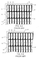
- a driver circuit (not shown) is typically associated with each ribbon element 101 for selectively applying a voltage thereto.
- ribbon element 121 represents an example of an actuated ribbon element.
- the driver associated with mirror 121 has applied a voltage to the electrode of ribbon element 121 , creating an electrostatic force ribbon element 121 and the common electrode on the back side of light valve 100 .
- This electrostatic force causes ribbon element 121 to deform into the cavity and to create a curved reflective surface as shown.
- Ribbon element 123 represents an example of a non-actuated ribbon element. Since there is no voltage applied to the electrode of ribbon element 123 , it is not deformed into the cavity and maintains a flat reflective surface as shown.
- Imaging head 115 also comprises a stop 116 and an imaging lens 118 .
- Stop 116 has a transmitting region 114 and a non-transmitting region 113 .
- the radiation from illumination line 106 is reflected from ribbon elements 101 of light valve 100 .
- a particular ribbon element for example, ribbon element 121
- its curved mirror surface focuses the reflected radiation, such that the reflected radiation travels through transmitting region 114 toward lens 118 .
- a particular ribbon element for example, ribbon element 122
- its flat mirror surface causes the reflected radiation to be dispersed and blocked by non-transmitting region 113 .
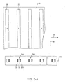
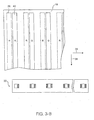
- Color filter 10 of FIG. 2-A comprises a substrate 18 which has been imaged with alternating elongated stripes (columns) 12, 14, 16 of red color elements R, green color elements G and blue color elements B .
- the individual color elements R, G, B are bounded by an opaque matrix layer 20 .
- matrix layer 20 outlines a two-dimensional matrix pattern of individual color elements R, G, B , wherein columns 12, 14, 16 of color elements have a single color and rows 13, 15, 17 of color elements have alternating colors.
- stripes 36 are imaged onto substrate 18 by scanning channel pattern 30 in the main scan direction indicated by arrow 38 .
- channel pattern 30 is stepped relative to substrate 18 in the sub-scan direction indicated by arrow 39.
- a new pass in the main scan direction 38 is then be commenced and the process is repeated until the entire desired area of substrate 18 is imaged.
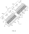
- Light valve 57 may be used in an imaging head (e.g. imaging head 115 of FIG. 1 ) to generate a channel pattern having high resolution channels and low resolution channels similar to the high resolution channels 33 and low resolution channels 32 of channel pattern 30 ( FIG. 3-A ).
- groups of ribbon elements having smaller numbers of individual ribbon elements 50 e.g. groups 133A, 133C
- groups of ribbon elements having larger numbers of individual ribbon elements 50 e.g. group 132B
- Each group of ribbon elements 50 connected to a single driver 58 may be referred to as a channel of light valve 57 .
- light valve 57 comprises a plurality of non-uniform channels, wherein smaller (high resolution) channels of light valve 57 correspond to groups of ribbon elements having smaller numbers of individual ribbon elements 50 and wherein larger (low resolution) channels of light valve 57 correspond to groups of ribbon elements having larger numbers of individual ribbon elements 50 .
- light valve 57 may comprise channels (i.e. groups of ribbon elements) having larger or smaller numbers of individual ribbon elements 50 or even a single individual ribbon element 50 . Each such group of ribbon elements may be independently actuated by a single driver.
- light valve 57 i.e. having one or more high resolution channels 133A, 133C on the outsides of a low resolution channel 132B
- light valve 57 is well suited for imaging the stripe pattern of FIG. 2-A and the mosaic pattern of FIG. 2-B .
- non-uniform channels i.e. groups of light valve elements with non-uniform numbers of individual light valve elements
Landscapes
- Physics & Mathematics (AREA)
- General Physics & Mathematics (AREA)
- Optics & Photonics (AREA)
- Engineering & Computer Science (AREA)
- Multimedia (AREA)
- Signal Processing (AREA)
- Nonlinear Science (AREA)
- Chemical & Material Sciences (AREA)
- Mathematical Physics (AREA)
- Crystallography & Structural Chemistry (AREA)
- Geometry (AREA)
- Mechanical Light Control Or Optical Switches (AREA)
- Optical Filters (AREA)
- Liquid Crystal (AREA)
- Devices For Indicating Variable Information By Combining Individual Elements (AREA)
- Glass Compositions (AREA)
- Vessels And Coating Films For Discharge Lamps (AREA)
- Length Measuring Devices By Optical Means (AREA)
Applications Claiming Priority (2)
| Application Number | Priority Date | Filing Date | Title |
|---|---|---|---|
| US10/628,887 US7042624B2 (en) | 2003-07-29 | 2003-07-29 | Non-uniform light valve |
| PCT/CA2004/001410 WO2005012976A1 (en) | 2003-07-29 | 2004-07-28 | Non-uniform light valve |
Publications (3)
| Publication Number | Publication Date |
|---|---|
| EP1664897A1 EP1664897A1 (en) | 2006-06-07 |
| EP1664897A4 EP1664897A4 (en) | 2008-03-12 |
| EP1664897B1 true EP1664897B1 (en) | 2011-05-25 |
Family
ID=34103473
Family Applications (1)
| Application Number | Title | Priority Date | Filing Date |
|---|---|---|---|
| EP04738017A Expired - Lifetime EP1664897B1 (en) | 2003-07-29 | 2004-07-28 | Non-uniform light valve |
Country Status (8)
Families Citing this family (4)
| Publication number | Priority date | Publication date | Assignee | Title |
|---|---|---|---|---|
| KR100712215B1 (ko) | 2005-08-25 | 2007-04-27 | 삼성에스디아이 주식회사 | 레이저 열전사용 마스크 및 그를 이용한 레이저 열전사방법 |
| GB2453682A (en) * | 2006-07-28 | 2009-04-15 | Kodak Graphic Comm Canada Co | Enhanced imaging of features |
| CN101970240B (zh) * | 2008-01-30 | 2013-02-27 | 加拿大柯达图形通信公司 | 一种用于在介质上形成图像的方法 |
| US8436882B2 (en) * | 2008-01-30 | 2013-05-07 | Kodak Graphic Communications Canada Company | Imaging features with skewed edges |
Family Cites Families (10)
| Publication number | Priority date | Publication date | Assignee | Title |
|---|---|---|---|---|
| US4374397A (en) * | 1981-06-01 | 1983-02-15 | Eastman Kodak Company | Light valve devices and electronic imaging/scan apparatus with locationally-interlaced optical addressing |
| US4965242A (en) | 1989-12-11 | 1990-10-23 | Eastman Kodak Company | Method of making color filter array for liquid crystal display |
| US5049901A (en) | 1990-07-02 | 1991-09-17 | Creo Products Inc. | Light modulator using large area light sources |
| DE69729659T2 (de) * | 1996-02-28 | 2005-06-23 | Johnson, Kenneth C., Santa Clara | Mikrolinsen-rastereinrichtung für mikrolithografie und für konfokale mikroskopie mit grossem aufnahmefeld |
| US6143451A (en) | 1996-11-26 | 2000-11-07 | E. I. Du Pont De Nemours And Company | Imaged laserable assemblages and associated processes with high speed and durable image-transfer characteristics for laser-induced thermal transfer |
| US6271957B1 (en) * | 1998-05-29 | 2001-08-07 | Affymetrix, Inc. | Methods involving direct write optical lithography |
| JP3706264B2 (ja) * | 1998-12-21 | 2005-10-12 | 日本放送協会 | 投射型マルチ画面ディスプレイ装置 |
| US6188519B1 (en) * | 1999-01-05 | 2001-02-13 | Kenneth Carlisle Johnson | Bigrating light valve |
| JP4308467B2 (ja) | 2001-12-27 | 2009-08-05 | 新光電気工業株式会社 | 露光方法及び露光装置 |
| US6728023B1 (en) * | 2002-05-28 | 2004-04-27 | Silicon Light Machines | Optical device arrays with optimized image resolution |
-
2003
- 2003-07-29 US US10/628,887 patent/US7042624B2/en not_active Expired - Fee Related
-
2004
- 2004-07-28 WO PCT/CA2004/001410 patent/WO2005012976A1/en active Application Filing
- 2004-07-28 JP JP2006521358A patent/JP4533377B2/ja not_active Expired - Fee Related
- 2004-07-28 EP EP04738017A patent/EP1664897B1/en not_active Expired - Lifetime
- 2004-07-28 KR KR1020067001937A patent/KR101045703B1/ko not_active Expired - Fee Related
- 2004-07-28 CN CNB2004800282977A patent/CN100434960C/zh not_active Expired - Fee Related
- 2004-07-28 AT AT04738017T patent/ATE511118T1/de not_active IP Right Cessation
- 2004-07-29 TW TW093122710A patent/TW200530625A/zh unknown
Also Published As
| Publication number | Publication date |
|---|---|
| WO2005012976A1 (en) | 2005-02-10 |
| CN100434960C (zh) | 2008-11-19 |
| EP1664897A4 (en) | 2008-03-12 |
| US7042624B2 (en) | 2006-05-09 |
| ATE511118T1 (de) | 2011-06-15 |
| EP1664897A1 (en) | 2006-06-07 |
| KR101045703B1 (ko) | 2011-06-30 |
| JP4533377B2 (ja) | 2010-09-01 |
| JP2007500366A (ja) | 2007-01-11 |
| TW200530625A (en) | 2005-09-16 |
| KR20060128818A (ko) | 2006-12-14 |
| CN1860401A (zh) | 2006-11-08 |
| US20050024706A1 (en) | 2005-02-03 |
Similar Documents
| Publication | Publication Date | Title |
|---|---|---|
| US6728023B1 (en) | Optical device arrays with optimized image resolution | |
| US7598008B2 (en) | Methods for imaging regular patterns | |
| US8305409B2 (en) | Forming an image with a plurality of imaging heads | |
| US8233020B2 (en) | Enhanced imaging of features | |
| EP1664897B1 (en) | Non-uniform light valve | |
| JP2011501814A (ja) | 可変な強さによる双方向画像形成 | |
| US20090309954A1 (en) | Methods and apparatus for selecting and applying non-contiguous features in a pattern | |
| EP2257437A2 (en) | Imaging patterns of features with varying resolutions | |
| EP1015250A1 (en) | Apparatus for reducing linear artifacts in an optically-printed image |
Legal Events
| Date | Code | Title | Description |
|---|---|---|---|
| PUAI | Public reference made under article 153(3) epc to a published international application that has entered the european phase |
Free format text: ORIGINAL CODE: 0009012 |
|
| 17P | Request for examination filed |
Effective date: 20060125 |
|
| AK | Designated contracting states |
Kind code of ref document: A1 Designated state(s): AT BE BG CH CY CZ DE DK EE ES FI FR GB GR HU IE IT LI LU MC NL PL PT RO SE SI SK TR |
|
| DAX | Request for extension of the european patent (deleted) | ||
| A4 | Supplementary search report drawn up and despatched |
Effective date: 20080207 |
|
| RIC1 | Information provided on ipc code assigned before grant |
Ipc: G02B 26/08 20060101AFI20050216BHEP Ipc: B41J 2/465 20060101ALI20080201BHEP Ipc: G02B 27/00 20060101ALI20080201BHEP |
|
| 17Q | First examination report despatched |
Effective date: 20090212 |
|
| GRAP | Despatch of communication of intention to grant a patent |
Free format text: ORIGINAL CODE: EPIDOSNIGR1 |
|
| GRAS | Grant fee paid |
Free format text: ORIGINAL CODE: EPIDOSNIGR3 |
|
| GRAA | (expected) grant |
Free format text: ORIGINAL CODE: 0009210 |
|
| AK | Designated contracting states |
Kind code of ref document: B1 Designated state(s): AT BE BG CH CY CZ DE DK EE ES FI FR GB GR HU IE IT LI LU MC NL PL PT RO SE SI SK TR |
|
| REG | Reference to a national code |
Ref country code: GB Ref legal event code: FG4D |
|
| REG | Reference to a national code |
Ref country code: CH Ref legal event code: EP |
|
| REG | Reference to a national code |
Ref country code: IE Ref legal event code: FG4D |
|
| REG | Reference to a national code |
Ref country code: DE Ref legal event code: R096 Ref document number: 602004032846 Country of ref document: DE Effective date: 20110707 |
|
| REG | Reference to a national code |
Ref country code: NL Ref legal event code: T3 |
|
| PG25 | Lapsed in a contracting state [announced via postgrant information from national office to epo] |
Ref country code: PT Free format text: LAPSE BECAUSE OF FAILURE TO SUBMIT A TRANSLATION OF THE DESCRIPTION OR TO PAY THE FEE WITHIN THE PRESCRIBED TIME-LIMIT Effective date: 20110926 Ref country code: SE Free format text: LAPSE BECAUSE OF FAILURE TO SUBMIT A TRANSLATION OF THE DESCRIPTION OR TO PAY THE FEE WITHIN THE PRESCRIBED TIME-LIMIT Effective date: 20110525 |
|
| PG25 | Lapsed in a contracting state [announced via postgrant information from national office to epo] |
Ref country code: FI Free format text: LAPSE BECAUSE OF FAILURE TO SUBMIT A TRANSLATION OF THE DESCRIPTION OR TO PAY THE FEE WITHIN THE PRESCRIBED TIME-LIMIT Effective date: 20110525 Ref country code: BE Free format text: LAPSE BECAUSE OF FAILURE TO SUBMIT A TRANSLATION OF THE DESCRIPTION OR TO PAY THE FEE WITHIN THE PRESCRIBED TIME-LIMIT Effective date: 20110525 Ref country code: ES Free format text: LAPSE BECAUSE OF FAILURE TO SUBMIT A TRANSLATION OF THE DESCRIPTION OR TO PAY THE FEE WITHIN THE PRESCRIBED TIME-LIMIT Effective date: 20110905 Ref country code: CY Free format text: LAPSE BECAUSE OF FAILURE TO SUBMIT A TRANSLATION OF THE DESCRIPTION OR TO PAY THE FEE WITHIN THE PRESCRIBED TIME-LIMIT Effective date: 20110525 Ref country code: SI Free format text: LAPSE BECAUSE OF FAILURE TO SUBMIT A TRANSLATION OF THE DESCRIPTION OR TO PAY THE FEE WITHIN THE PRESCRIBED TIME-LIMIT Effective date: 20110525 Ref country code: AT Free format text: LAPSE BECAUSE OF FAILURE TO SUBMIT A TRANSLATION OF THE DESCRIPTION OR TO PAY THE FEE WITHIN THE PRESCRIBED TIME-LIMIT Effective date: 20110525 Ref country code: GR Free format text: LAPSE BECAUSE OF FAILURE TO SUBMIT A TRANSLATION OF THE DESCRIPTION OR TO PAY THE FEE WITHIN THE PRESCRIBED TIME-LIMIT Effective date: 20110826 |
|
| PG25 | Lapsed in a contracting state [announced via postgrant information from national office to epo] |
Ref country code: CZ Free format text: LAPSE BECAUSE OF FAILURE TO SUBMIT A TRANSLATION OF THE DESCRIPTION OR TO PAY THE FEE WITHIN THE PRESCRIBED TIME-LIMIT Effective date: 20110525 Ref country code: EE Free format text: LAPSE BECAUSE OF FAILURE TO SUBMIT A TRANSLATION OF THE DESCRIPTION OR TO PAY THE FEE WITHIN THE PRESCRIBED TIME-LIMIT Effective date: 20110525 |
|
| PG25 | Lapsed in a contracting state [announced via postgrant information from national office to epo] |
Ref country code: RO Free format text: LAPSE BECAUSE OF FAILURE TO SUBMIT A TRANSLATION OF THE DESCRIPTION OR TO PAY THE FEE WITHIN THE PRESCRIBED TIME-LIMIT Effective date: 20110525 Ref country code: PL Free format text: LAPSE BECAUSE OF FAILURE TO SUBMIT A TRANSLATION OF THE DESCRIPTION OR TO PAY THE FEE WITHIN THE PRESCRIBED TIME-LIMIT Effective date: 20110525 Ref country code: DK Free format text: LAPSE BECAUSE OF FAILURE TO SUBMIT A TRANSLATION OF THE DESCRIPTION OR TO PAY THE FEE WITHIN THE PRESCRIBED TIME-LIMIT Effective date: 20110525 Ref country code: MC Free format text: LAPSE BECAUSE OF NON-PAYMENT OF DUE FEES Effective date: 20110731 Ref country code: SK Free format text: LAPSE BECAUSE OF FAILURE TO SUBMIT A TRANSLATION OF THE DESCRIPTION OR TO PAY THE FEE WITHIN THE PRESCRIBED TIME-LIMIT Effective date: 20110525 |
|
| REG | Reference to a national code |
Ref country code: CH Ref legal event code: PL |
|
| PLBE | No opposition filed within time limit |
Free format text: ORIGINAL CODE: 0009261 |
|
| STAA | Information on the status of an ep patent application or granted ep patent |
Free format text: STATUS: NO OPPOSITION FILED WITHIN TIME LIMIT |
|
| REG | Reference to a national code |
Ref country code: FR Ref legal event code: ST Effective date: 20120330 |
|
| REG | Reference to a national code |
Ref country code: IE Ref legal event code: MM4A |
|
| PG25 | Lapsed in a contracting state [announced via postgrant information from national office to epo] |
Ref country code: LI Free format text: LAPSE BECAUSE OF NON-PAYMENT OF DUE FEES Effective date: 20110731 Ref country code: FR Free format text: LAPSE BECAUSE OF NON-PAYMENT OF DUE FEES Effective date: 20110801 Ref country code: CH Free format text: LAPSE BECAUSE OF NON-PAYMENT OF DUE FEES Effective date: 20110731 |
|
| 26N | No opposition filed |
Effective date: 20120228 |
|
| PG25 | Lapsed in a contracting state [announced via postgrant information from national office to epo] |
Ref country code: IT Free format text: LAPSE BECAUSE OF FAILURE TO SUBMIT A TRANSLATION OF THE DESCRIPTION OR TO PAY THE FEE WITHIN THE PRESCRIBED TIME-LIMIT Effective date: 20110525 |
|
| REG | Reference to a national code |
Ref country code: DE Ref legal event code: R097 Ref document number: 602004032846 Country of ref document: DE Effective date: 20120228 |
|
| PG25 | Lapsed in a contracting state [announced via postgrant information from national office to epo] |
Ref country code: IE Free format text: LAPSE BECAUSE OF NON-PAYMENT OF DUE FEES Effective date: 20110728 |
|
| PGFP | Annual fee paid to national office [announced via postgrant information from national office to epo] |
Ref country code: GB Payment date: 20120625 Year of fee payment: 9 |
|
| PG25 | Lapsed in a contracting state [announced via postgrant information from national office to epo] |
Ref country code: LU Free format text: LAPSE BECAUSE OF NON-PAYMENT OF DUE FEES Effective date: 20110728 |
|
| PG25 | Lapsed in a contracting state [announced via postgrant information from national office to epo] |
Ref country code: BG Free format text: LAPSE BECAUSE OF FAILURE TO SUBMIT A TRANSLATION OF THE DESCRIPTION OR TO PAY THE FEE WITHIN THE PRESCRIBED TIME-LIMIT Effective date: 20110825 |
|
| PG25 | Lapsed in a contracting state [announced via postgrant information from national office to epo] |
Ref country code: TR Free format text: LAPSE BECAUSE OF FAILURE TO SUBMIT A TRANSLATION OF THE DESCRIPTION OR TO PAY THE FEE WITHIN THE PRESCRIBED TIME-LIMIT Effective date: 20110525 |
|
| PG25 | Lapsed in a contracting state [announced via postgrant information from national office to epo] |
Ref country code: HU Free format text: LAPSE BECAUSE OF FAILURE TO SUBMIT A TRANSLATION OF THE DESCRIPTION OR TO PAY THE FEE WITHIN THE PRESCRIBED TIME-LIMIT Effective date: 20110525 |
|
| PGFP | Annual fee paid to national office [announced via postgrant information from national office to epo] |
Ref country code: NL Payment date: 20130711 Year of fee payment: 10 Ref country code: DE Payment date: 20130731 Year of fee payment: 10 |
|
| GBPC | Gb: european patent ceased through non-payment of renewal fee |
Effective date: 20130728 |
|
| PG25 | Lapsed in a contracting state [announced via postgrant information from national office to epo] |
Ref country code: GB Free format text: LAPSE BECAUSE OF NON-PAYMENT OF DUE FEES Effective date: 20130728 |
|
| REG | Reference to a national code |
Ref country code: DE Ref legal event code: R119 Ref document number: 602004032846 Country of ref document: DE |
|
| REG | Reference to a national code |
Ref country code: NL Ref legal event code: V1 Effective date: 20150201 |
|
| PG25 | Lapsed in a contracting state [announced via postgrant information from national office to epo] |
Ref country code: NL Free format text: LAPSE BECAUSE OF NON-PAYMENT OF DUE FEES Effective date: 20150201 |
|
| PG25 | Lapsed in a contracting state [announced via postgrant information from national office to epo] |
Ref country code: DE Free format text: LAPSE BECAUSE OF NON-PAYMENT OF DUE FEES Effective date: 20150203 |
|
| REG | Reference to a national code |
Ref country code: DE Ref legal event code: R119 Ref document number: 602004032846 Country of ref document: DE Effective date: 20150203 |