EP1653503A2 - Semiconductor device, circuit board, electro-optic device, electronic device - Google Patents
Semiconductor device, circuit board, electro-optic device, electronic device Download PDFInfo
- Publication number
- EP1653503A2 EP1653503A2 EP05023273A EP05023273A EP1653503A2 EP 1653503 A2 EP1653503 A2 EP 1653503A2 EP 05023273 A EP05023273 A EP 05023273A EP 05023273 A EP05023273 A EP 05023273A EP 1653503 A2 EP1653503 A2 EP 1653503A2
- Authority
- EP
- European Patent Office
- Prior art keywords
- conductive layer
- resin bump
- semiconductor device
- resin
- bump
- Prior art date
- Legal status (The legal status is an assumption and is not a legal conclusion. Google has not performed a legal analysis and makes no representation as to the accuracy of the status listed.)
- Withdrawn
Links
Images



Classifications
-
- H—ELECTRICITY
- H10—SEMICONDUCTOR DEVICES; ELECTRIC SOLID-STATE DEVICES NOT OTHERWISE PROVIDED FOR
- H10W—GENERIC PACKAGES, INTERCONNECTIONS, CONNECTORS OR OTHER CONSTRUCTIONAL DETAILS OF DEVICES COVERED BY CLASS H10
- H10W42/00—Arrangements for protection of devices
- H10W42/121—Arrangements for protection of devices protecting against mechanical damage
-
- G—PHYSICS
- G02—OPTICS
- G02F—OPTICAL DEVICES OR ARRANGEMENTS FOR THE CONTROL OF LIGHT BY MODIFICATION OF THE OPTICAL PROPERTIES OF THE MEDIA OF THE ELEMENTS INVOLVED THEREIN; NON-LINEAR OPTICS; FREQUENCY-CHANGING OF LIGHT; OPTICAL LOGIC ELEMENTS; OPTICAL ANALOGUE/DIGITAL CONVERTERS
- G02F1/00—Devices or arrangements for the control of the intensity, colour, phase, polarisation or direction of light arriving from an independent light source, e.g. switching, gating or modulating; Non-linear optics
- G02F1/01—Devices or arrangements for the control of the intensity, colour, phase, polarisation or direction of light arriving from an independent light source, e.g. switching, gating or modulating; Non-linear optics for the control of the intensity, phase, polarisation or colour
- G02F1/13—Devices or arrangements for the control of the intensity, colour, phase, polarisation or direction of light arriving from an independent light source, e.g. switching, gating or modulating; Non-linear optics for the control of the intensity, phase, polarisation or colour based on liquid crystals, e.g. single liquid crystal display cells
- G02F1/133—Constructional arrangements; Operation of liquid crystal cells; Circuit arrangements
- G02F1/1333—Constructional arrangements; Manufacturing methods
- G02F1/1345—Conductors connecting electrodes to cell terminals
- G02F1/13458—Terminal pads
-
- H—ELECTRICITY
- H10—SEMICONDUCTOR DEVICES; ELECTRIC SOLID-STATE DEVICES NOT OTHERWISE PROVIDED FOR
- H10W—GENERIC PACKAGES, INTERCONNECTIONS, CONNECTORS OR OTHER CONSTRUCTIONAL DETAILS OF DEVICES COVERED BY CLASS H10
- H10W72/00—Interconnections or connectors in packages
-
- H—ELECTRICITY
- H10—SEMICONDUCTOR DEVICES; ELECTRIC SOLID-STATE DEVICES NOT OTHERWISE PROVIDED FOR
- H10W—GENERIC PACKAGES, INTERCONNECTIONS, CONNECTORS OR OTHER CONSTRUCTIONAL DETAILS OF DEVICES COVERED BY CLASS H10
- H10W72/00—Interconnections or connectors in packages
- H10W72/071—Connecting or disconnecting
- H10W72/072—Connecting or disconnecting of bump connectors
-
- H—ELECTRICITY
- H10—SEMICONDUCTOR DEVICES; ELECTRIC SOLID-STATE DEVICES NOT OTHERWISE PROVIDED FOR
- H10W—GENERIC PACKAGES, INTERCONNECTIONS, CONNECTORS OR OTHER CONSTRUCTIONAL DETAILS OF DEVICES COVERED BY CLASS H10
- H10W74/00—Encapsulations, e.g. protective coatings
- H10W74/01—Manufacture or treatment
- H10W74/012—Manufacture or treatment of encapsulations on active surfaces of flip-chip devices, e.g. forming underfills
-
- H—ELECTRICITY
- H10—SEMICONDUCTOR DEVICES; ELECTRIC SOLID-STATE DEVICES NOT OTHERWISE PROVIDED FOR
- H10W—GENERIC PACKAGES, INTERCONNECTIONS, CONNECTORS OR OTHER CONSTRUCTIONAL DETAILS OF DEVICES COVERED BY CLASS H10
- H10W74/00—Encapsulations, e.g. protective coatings
- H10W74/10—Encapsulations, e.g. protective coatings characterised by their shape or disposition
- H10W74/15—Encapsulations, e.g. protective coatings characterised by their shape or disposition on active surfaces of flip-chip devices, e.g. underfills
-
- H—ELECTRICITY
- H10—SEMICONDUCTOR DEVICES; ELECTRIC SOLID-STATE DEVICES NOT OTHERWISE PROVIDED FOR
- H10W—GENERIC PACKAGES, INTERCONNECTIONS, CONNECTORS OR OTHER CONSTRUCTIONAL DETAILS OF DEVICES COVERED BY CLASS H10
- H10W99/00—Subject matter not provided for in other groups of this subclass
-
- H—ELECTRICITY
- H10—SEMICONDUCTOR DEVICES; ELECTRIC SOLID-STATE DEVICES NOT OTHERWISE PROVIDED FOR
- H10W—GENERIC PACKAGES, INTERCONNECTIONS, CONNECTORS OR OTHER CONSTRUCTIONAL DETAILS OF DEVICES COVERED BY CLASS H10
- H10W70/00—Package substrates; Interposers; Redistribution layers [RDL]
- H10W70/01—Manufacture or treatment
- H10W70/05—Manufacture or treatment of insulating or insulated package substrates, or of interposers, or of redistribution layers
-
- H—ELECTRICITY
- H10—SEMICONDUCTOR DEVICES; ELECTRIC SOLID-STATE DEVICES NOT OTHERWISE PROVIDED FOR
- H10W—GENERIC PACKAGES, INTERCONNECTIONS, CONNECTORS OR OTHER CONSTRUCTIONAL DETAILS OF DEVICES COVERED BY CLASS H10
- H10W70/00—Package substrates; Interposers; Redistribution layers [RDL]
- H10W70/60—Insulating or insulated package substrates; Interposers; Redistribution layers
-
- H—ELECTRICITY
- H10—SEMICONDUCTOR DEVICES; ELECTRIC SOLID-STATE DEVICES NOT OTHERWISE PROVIDED FOR
- H10W—GENERIC PACKAGES, INTERCONNECTIONS, CONNECTORS OR OTHER CONSTRUCTIONAL DETAILS OF DEVICES COVERED BY CLASS H10
- H10W70/00—Package substrates; Interposers; Redistribution layers [RDL]
- H10W70/60—Insulating or insulated package substrates; Interposers; Redistribution layers
- H10W70/62—Insulating or insulated package substrates; Interposers; Redistribution layers characterised by their interconnections
- H10W70/65—Shapes or dispositions of interconnections
- H10W70/654—Top-view layouts
- H10W70/656—Fan-in layouts
-
- H—ELECTRICITY
- H10—SEMICONDUCTOR DEVICES; ELECTRIC SOLID-STATE DEVICES NOT OTHERWISE PROVIDED FOR
- H10W—GENERIC PACKAGES, INTERCONNECTIONS, CONNECTORS OR OTHER CONSTRUCTIONAL DETAILS OF DEVICES COVERED BY CLASS H10
- H10W70/00—Package substrates; Interposers; Redistribution layers [RDL]
- H10W70/60—Insulating or insulated package substrates; Interposers; Redistribution layers
- H10W70/62—Insulating or insulated package substrates; Interposers; Redistribution layers characterised by their interconnections
- H10W70/66—Conductive materials thereof
-
- H—ELECTRICITY
- H10—SEMICONDUCTOR DEVICES; ELECTRIC SOLID-STATE DEVICES NOT OTHERWISE PROVIDED FOR
- H10W—GENERIC PACKAGES, INTERCONNECTIONS, CONNECTORS OR OTHER CONSTRUCTIONAL DETAILS OF DEVICES COVERED BY CLASS H10
- H10W70/00—Package substrates; Interposers; Redistribution layers [RDL]
- H10W70/60—Insulating or insulated package substrates; Interposers; Redistribution layers
- H10W70/67—Insulating or insulated package substrates; Interposers; Redistribution layers characterised by their insulating layers or insulating parts
- H10W70/68—Shapes or dispositions thereof
-
- H—ELECTRICITY
- H10—SEMICONDUCTOR DEVICES; ELECTRIC SOLID-STATE DEVICES NOT OTHERWISE PROVIDED FOR
- H10W—GENERIC PACKAGES, INTERCONNECTIONS, CONNECTORS OR OTHER CONSTRUCTIONAL DETAILS OF DEVICES COVERED BY CLASS H10
- H10W70/00—Package substrates; Interposers; Redistribution layers [RDL]
- H10W70/60—Insulating or insulated package substrates; Interposers; Redistribution layers
- H10W70/67—Insulating or insulated package substrates; Interposers; Redistribution layers characterised by their insulating layers or insulating parts
- H10W70/69—Insulating materials thereof
-
- H—ELECTRICITY
- H10—SEMICONDUCTOR DEVICES; ELECTRIC SOLID-STATE DEVICES NOT OTHERWISE PROVIDED FOR
- H10W—GENERIC PACKAGES, INTERCONNECTIONS, CONNECTORS OR OTHER CONSTRUCTIONAL DETAILS OF DEVICES COVERED BY CLASS H10
- H10W72/00—Interconnections or connectors in packages
- H10W72/01—Manufacture or treatment
- H10W72/012—Manufacture or treatment of bump connectors, dummy bumps or thermal bumps
- H10W72/01231—Manufacture or treatment of bump connectors, dummy bumps or thermal bumps using blanket deposition
-
- H—ELECTRICITY
- H10—SEMICONDUCTOR DEVICES; ELECTRIC SOLID-STATE DEVICES NOT OTHERWISE PROVIDED FOR
- H10W—GENERIC PACKAGES, INTERCONNECTIONS, CONNECTORS OR OTHER CONSTRUCTIONAL DETAILS OF DEVICES COVERED BY CLASS H10
- H10W72/00—Interconnections or connectors in packages
- H10W72/01—Manufacture or treatment
- H10W72/012—Manufacture or treatment of bump connectors, dummy bumps or thermal bumps
- H10W72/01251—Changing the shapes of bumps
-
- H—ELECTRICITY
- H10—SEMICONDUCTOR DEVICES; ELECTRIC SOLID-STATE DEVICES NOT OTHERWISE PROVIDED FOR
- H10W—GENERIC PACKAGES, INTERCONNECTIONS, CONNECTORS OR OTHER CONSTRUCTIONAL DETAILS OF DEVICES COVERED BY CLASS H10
- H10W72/00—Interconnections or connectors in packages
- H10W72/01—Manufacture or treatment
- H10W72/013—Manufacture or treatment of die-attach connectors
- H10W72/01315—Forming coatings
-
- H—ELECTRICITY
- H10—SEMICONDUCTOR DEVICES; ELECTRIC SOLID-STATE DEVICES NOT OTHERWISE PROVIDED FOR
- H10W—GENERIC PACKAGES, INTERCONNECTIONS, CONNECTORS OR OTHER CONSTRUCTIONAL DETAILS OF DEVICES COVERED BY CLASS H10
- H10W72/00—Interconnections or connectors in packages
- H10W72/01—Manufacture or treatment
- H10W72/013—Manufacture or treatment of die-attach connectors
- H10W72/01351—Changing the shapes of die-attach connectors
- H10W72/01353—Changing the shapes of die-attach connectors by etching
-
- H—ELECTRICITY
- H10—SEMICONDUCTOR DEVICES; ELECTRIC SOLID-STATE DEVICES NOT OTHERWISE PROVIDED FOR
- H10W—GENERIC PACKAGES, INTERCONNECTIONS, CONNECTORS OR OTHER CONSTRUCTIONAL DETAILS OF DEVICES COVERED BY CLASS H10
- H10W72/00—Interconnections or connectors in packages
- H10W72/071—Connecting or disconnecting
- H10W72/073—Connecting or disconnecting of die-attach connectors
-
- H—ELECTRICITY
- H10—SEMICONDUCTOR DEVICES; ELECTRIC SOLID-STATE DEVICES NOT OTHERWISE PROVIDED FOR
- H10W—GENERIC PACKAGES, INTERCONNECTIONS, CONNECTORS OR OTHER CONSTRUCTIONAL DETAILS OF DEVICES COVERED BY CLASS H10
- H10W72/00—Interconnections or connectors in packages
- H10W72/071—Connecting or disconnecting
- H10W72/073—Connecting or disconnecting of die-attach connectors
- H10W72/07331—Connecting techniques
- H10W72/07337—Connecting techniques using a polymer adhesive, e.g. an adhesive based on silicone or epoxy
- H10W72/07338—Connecting techniques using a polymer adhesive, e.g. an adhesive based on silicone or epoxy hardening the adhesive by curing, e.g. thermosetting
-
- H—ELECTRICITY
- H10—SEMICONDUCTOR DEVICES; ELECTRIC SOLID-STATE DEVICES NOT OTHERWISE PROVIDED FOR
- H10W—GENERIC PACKAGES, INTERCONNECTIONS, CONNECTORS OR OTHER CONSTRUCTIONAL DETAILS OF DEVICES COVERED BY CLASS H10
- H10W72/00—Interconnections or connectors in packages
- H10W72/20—Bump connectors, e.g. solder bumps or copper pillars; Dummy bumps; Thermal bumps
-
- H—ELECTRICITY
- H10—SEMICONDUCTOR DEVICES; ELECTRIC SOLID-STATE DEVICES NOT OTHERWISE PROVIDED FOR
- H10W—GENERIC PACKAGES, INTERCONNECTIONS, CONNECTORS OR OTHER CONSTRUCTIONAL DETAILS OF DEVICES COVERED BY CLASS H10
- H10W72/00—Interconnections or connectors in packages
- H10W72/20—Bump connectors, e.g. solder bumps or copper pillars; Dummy bumps; Thermal bumps
- H10W72/231—Shapes
- H10W72/234—Cross-sectional shape, i.e. in side view
-
- H—ELECTRICITY
- H10—SEMICONDUCTOR DEVICES; ELECTRIC SOLID-STATE DEVICES NOT OTHERWISE PROVIDED FOR
- H10W—GENERIC PACKAGES, INTERCONNECTIONS, CONNECTORS OR OTHER CONSTRUCTIONAL DETAILS OF DEVICES COVERED BY CLASS H10
- H10W72/00—Interconnections or connectors in packages
- H10W72/20—Bump connectors, e.g. solder bumps or copper pillars; Dummy bumps; Thermal bumps
- H10W72/251—Materials
-
- H—ELECTRICITY
- H10—SEMICONDUCTOR DEVICES; ELECTRIC SOLID-STATE DEVICES NOT OTHERWISE PROVIDED FOR
- H10W—GENERIC PACKAGES, INTERCONNECTIONS, CONNECTORS OR OTHER CONSTRUCTIONAL DETAILS OF DEVICES COVERED BY CLASS H10
- H10W72/00—Interconnections or connectors in packages
- H10W72/20—Bump connectors, e.g. solder bumps or copper pillars; Dummy bumps; Thermal bumps
- H10W72/251—Materials
- H10W72/252—Materials comprising solid metals or solid metalloids, e.g. PbSn, Ag or Cu
-
- H—ELECTRICITY
- H10—SEMICONDUCTOR DEVICES; ELECTRIC SOLID-STATE DEVICES NOT OTHERWISE PROVIDED FOR
- H10W—GENERIC PACKAGES, INTERCONNECTIONS, CONNECTORS OR OTHER CONSTRUCTIONAL DETAILS OF DEVICES COVERED BY CLASS H10
- H10W72/00—Interconnections or connectors in packages
- H10W72/20—Bump connectors, e.g. solder bumps or copper pillars; Dummy bumps; Thermal bumps
- H10W72/251—Materials
- H10W72/253—Materials not comprising solid metals or solid metalloids, e.g. polymers or ceramics
-
- H—ELECTRICITY
- H10—SEMICONDUCTOR DEVICES; ELECTRIC SOLID-STATE DEVICES NOT OTHERWISE PROVIDED FOR
- H10W—GENERIC PACKAGES, INTERCONNECTIONS, CONNECTORS OR OTHER CONSTRUCTIONAL DETAILS OF DEVICES COVERED BY CLASS H10
- H10W72/00—Interconnections or connectors in packages
- H10W72/20—Bump connectors, e.g. solder bumps or copper pillars; Dummy bumps; Thermal bumps
- H10W72/251—Materials
- H10W72/255—Materials of outermost layers of multilayered bumps, e.g. material of a coating
-
- H—ELECTRICITY
- H10—SEMICONDUCTOR DEVICES; ELECTRIC SOLID-STATE DEVICES NOT OTHERWISE PROVIDED FOR
- H10W—GENERIC PACKAGES, INTERCONNECTIONS, CONNECTORS OR OTHER CONSTRUCTIONAL DETAILS OF DEVICES COVERED BY CLASS H10
- H10W72/00—Interconnections or connectors in packages
- H10W72/20—Bump connectors, e.g. solder bumps or copper pillars; Dummy bumps; Thermal bumps
- H10W72/29—Bond pads specially adapted therefor
-
- H—ELECTRICITY
- H10—SEMICONDUCTOR DEVICES; ELECTRIC SOLID-STATE DEVICES NOT OTHERWISE PROVIDED FOR
- H10W—GENERIC PACKAGES, INTERCONNECTIONS, CONNECTORS OR OTHER CONSTRUCTIONAL DETAILS OF DEVICES COVERED BY CLASS H10
- H10W72/00—Interconnections or connectors in packages
- H10W72/30—Die-attach connectors
- H10W72/321—Structures or relative sizes of die-attach connectors
-
- H—ELECTRICITY
- H10—SEMICONDUCTOR DEVICES; ELECTRIC SOLID-STATE DEVICES NOT OTHERWISE PROVIDED FOR
- H10W—GENERIC PACKAGES, INTERCONNECTIONS, CONNECTORS OR OTHER CONSTRUCTIONAL DETAILS OF DEVICES COVERED BY CLASS H10
- H10W72/00—Interconnections or connectors in packages
- H10W72/30—Die-attach connectors
- H10W72/321—Structures or relative sizes of die-attach connectors
- H10W72/322—Multilayered die-attach connectors, e.g. a coating on a top surface of a core
-
- H—ELECTRICITY
- H10—SEMICONDUCTOR DEVICES; ELECTRIC SOLID-STATE DEVICES NOT OTHERWISE PROVIDED FOR
- H10W—GENERIC PACKAGES, INTERCONNECTIONS, CONNECTORS OR OTHER CONSTRUCTIONAL DETAILS OF DEVICES COVERED BY CLASS H10
- H10W72/00—Interconnections or connectors in packages
- H10W72/30—Die-attach connectors
- H10W72/321—Structures or relative sizes of die-attach connectors
- H10W72/322—Multilayered die-attach connectors, e.g. a coating on a top surface of a core
- H10W72/323—Multilayered die-attach connectors, e.g. a coating on a top surface of a core characterised by the structures of the outermost layers, e.g. multilayered coatings
-
- H—ELECTRICITY
- H10—SEMICONDUCTOR DEVICES; ELECTRIC SOLID-STATE DEVICES NOT OTHERWISE PROVIDED FOR
- H10W—GENERIC PACKAGES, INTERCONNECTIONS, CONNECTORS OR OTHER CONSTRUCTIONAL DETAILS OF DEVICES COVERED BY CLASS H10
- H10W72/00—Interconnections or connectors in packages
- H10W72/30—Die-attach connectors
- H10W72/331—Shapes of die-attach connectors
- H10W72/332—Plan-view shape, i.e. in top view
-
- H—ELECTRICITY
- H10—SEMICONDUCTOR DEVICES; ELECTRIC SOLID-STATE DEVICES NOT OTHERWISE PROVIDED FOR
- H10W—GENERIC PACKAGES, INTERCONNECTIONS, CONNECTORS OR OTHER CONSTRUCTIONAL DETAILS OF DEVICES COVERED BY CLASS H10
- H10W72/00—Interconnections or connectors in packages
- H10W72/30—Die-attach connectors
- H10W72/331—Shapes of die-attach connectors
- H10W72/334—Cross-sectional shape, i.e. in side view
-
- H—ELECTRICITY
- H10—SEMICONDUCTOR DEVICES; ELECTRIC SOLID-STATE DEVICES NOT OTHERWISE PROVIDED FOR
- H10W—GENERIC PACKAGES, INTERCONNECTIONS, CONNECTORS OR OTHER CONSTRUCTIONAL DETAILS OF DEVICES COVERED BY CLASS H10
- H10W72/00—Interconnections or connectors in packages
- H10W72/30—Die-attach connectors
- H10W72/341—Dispositions of die-attach connectors, e.g. layouts
- H10W72/342—Dispositions of die-attach connectors, e.g. layouts relative to the surface, e.g. recessed, protruding
-
- H—ELECTRICITY
- H10—SEMICONDUCTOR DEVICES; ELECTRIC SOLID-STATE DEVICES NOT OTHERWISE PROVIDED FOR
- H10W—GENERIC PACKAGES, INTERCONNECTIONS, CONNECTORS OR OTHER CONSTRUCTIONAL DETAILS OF DEVICES COVERED BY CLASS H10
- H10W72/00—Interconnections or connectors in packages
- H10W72/30—Die-attach connectors
- H10W72/341—Dispositions of die-attach connectors, e.g. layouts
- H10W72/345—Dispositions of die-attach connectors, e.g. layouts of outermost layers of multilayered die-attach connectors, e.g. coating being only on a part of a core
-
- H—ELECTRICITY
- H10—SEMICONDUCTOR DEVICES; ELECTRIC SOLID-STATE DEVICES NOT OTHERWISE PROVIDED FOR
- H10W—GENERIC PACKAGES, INTERCONNECTIONS, CONNECTORS OR OTHER CONSTRUCTIONAL DETAILS OF DEVICES COVERED BY CLASS H10
- H10W72/00—Interconnections or connectors in packages
- H10W72/30—Die-attach connectors
- H10W72/341—Dispositions of die-attach connectors, e.g. layouts
- H10W72/347—Dispositions of multiple die-attach connectors
- H10W72/348—Top-view layouts, e.g. mirror arrays
-
- H—ELECTRICITY
- H10—SEMICONDUCTOR DEVICES; ELECTRIC SOLID-STATE DEVICES NOT OTHERWISE PROVIDED FOR
- H10W—GENERIC PACKAGES, INTERCONNECTIONS, CONNECTORS OR OTHER CONSTRUCTIONAL DETAILS OF DEVICES COVERED BY CLASS H10
- H10W72/00—Interconnections or connectors in packages
- H10W72/30—Die-attach connectors
- H10W72/351—Materials of die-attach connectors
- H10W72/352—Materials of die-attach connectors comprising metals or metalloids, e.g. solders
-
- H—ELECTRICITY
- H10—SEMICONDUCTOR DEVICES; ELECTRIC SOLID-STATE DEVICES NOT OTHERWISE PROVIDED FOR
- H10W—GENERIC PACKAGES, INTERCONNECTIONS, CONNECTORS OR OTHER CONSTRUCTIONAL DETAILS OF DEVICES COVERED BY CLASS H10
- H10W72/00—Interconnections or connectors in packages
- H10W72/30—Die-attach connectors
- H10W72/351—Materials of die-attach connectors
- H10W72/353—Materials of die-attach connectors not comprising solid metals or solid metalloids, e.g. ceramics
-
- H—ELECTRICITY
- H10—SEMICONDUCTOR DEVICES; ELECTRIC SOLID-STATE DEVICES NOT OTHERWISE PROVIDED FOR
- H10W—GENERIC PACKAGES, INTERCONNECTIONS, CONNECTORS OR OTHER CONSTRUCTIONAL DETAILS OF DEVICES COVERED BY CLASS H10
- H10W72/00—Interconnections or connectors in packages
- H10W72/30—Die-attach connectors
- H10W72/351—Materials of die-attach connectors
- H10W72/353—Materials of die-attach connectors not comprising solid metals or solid metalloids, e.g. ceramics
- H10W72/354—Materials of die-attach connectors not comprising solid metals or solid metalloids, e.g. ceramics comprising polymers
-
- H—ELECTRICITY
- H10—SEMICONDUCTOR DEVICES; ELECTRIC SOLID-STATE DEVICES NOT OTHERWISE PROVIDED FOR
- H10W—GENERIC PACKAGES, INTERCONNECTIONS, CONNECTORS OR OTHER CONSTRUCTIONAL DETAILS OF DEVICES COVERED BY CLASS H10
- H10W72/00—Interconnections or connectors in packages
- H10W72/30—Die-attach connectors
- H10W72/351—Materials of die-attach connectors
- H10W72/355—Materials of die-attach connectors of outermost layers of multilayered die-attach connectors, e.g. material of a coating
-
- H—ELECTRICITY
- H10—SEMICONDUCTOR DEVICES; ELECTRIC SOLID-STATE DEVICES NOT OTHERWISE PROVIDED FOR
- H10W—GENERIC PACKAGES, INTERCONNECTIONS, CONNECTORS OR OTHER CONSTRUCTIONAL DETAILS OF DEVICES COVERED BY CLASS H10
- H10W72/00—Interconnections or connectors in packages
- H10W72/90—Bond pads, in general
-
- H—ELECTRICITY
- H10—SEMICONDUCTOR DEVICES; ELECTRIC SOLID-STATE DEVICES NOT OTHERWISE PROVIDED FOR
- H10W—GENERIC PACKAGES, INTERCONNECTIONS, CONNECTORS OR OTHER CONSTRUCTIONAL DETAILS OF DEVICES COVERED BY CLASS H10
- H10W90/00—Package configurations
- H10W90/701—Package configurations characterised by the relative positions of pads or connectors relative to package parts
- H10W90/721—Package configurations characterised by the relative positions of pads or connectors relative to package parts of bump connectors
- H10W90/724—Package configurations characterised by the relative positions of pads or connectors relative to package parts of bump connectors between a chip and a stacked insulating package substrate, interposer or RDL
-
- H—ELECTRICITY
- H10—SEMICONDUCTOR DEVICES; ELECTRIC SOLID-STATE DEVICES NOT OTHERWISE PROVIDED FOR
- H10W—GENERIC PACKAGES, INTERCONNECTIONS, CONNECTORS OR OTHER CONSTRUCTIONAL DETAILS OF DEVICES COVERED BY CLASS H10
- H10W90/00—Package configurations
- H10W90/701—Package configurations characterised by the relative positions of pads or connectors relative to package parts
- H10W90/731—Package configurations characterised by the relative positions of pads or connectors relative to package parts of die-attach connectors
- H10W90/734—Package configurations characterised by the relative positions of pads or connectors relative to package parts of die-attach connectors between a chip and a stacked insulating package substrate, interposer or RDL
Definitions
- the present invention relates to a semiconductor device and its manufacturing method, a circuit board, an electro-optic device and an electronic device.
- IC chips integrated circuit chips
- a glass board the partner board which is a component of the liquid crystal panel (a so-called COG structure).
- COG structure a component of the liquid crystal panel
- an IC chip made of hard silicon board is mounted on a hard glass board, it is hard to absorb warpage of the IC chip and the glass board.
- bump electrodes are formed on the IC chip, and the IC chip is mounted on the glass board by compressing the bump electrodes. This process enables the IC chip and the glass board to be conductively connected.
- a resin bump electrode 10 shown in FIG. 8 has been developed.
- the resin bump electrode 10 is made by forming a conducting layer 20 on a resin bump 12, and the conducting layer 20 is connected to an electrode pad 24 of an IC chip 21 (for example, refer to Japanese Unexamined Patent Application, First Publication No. H01-13734).
- the resin bump electrode 10 makes elastic deformation by contacting a partner board, and the warpage of the IC chip 21 and the partner board can be absorbed. Since this process does not require enlargement of the aspect ratio of the aperture, it is easier to narrow pitches between bump electrodes than in an ordinary method.
- the resin bump 12 has high coefficient of thermal expansion, when carrying out a hot press bond of the IC chip 21 and the partner board, the conductive layer 20 receives great tensile stress due to deforming following the expansion of the resin bump 12.
- the present invention provides a semiconductor device including a semiconductor element, an electrode pad formed on the semiconductor element, and a bump electrode conductively connected to the electrode pad which includes a resin bump formed on an active face of the semiconductor element, and a conductive layer provided from the electrode pad to the surface of the resin bump, the conductive layer and the resin bump being arranged without adhesion.
- a material with high ductibility such as Au is suitable for the conductive layer.
- the conductive layer is free from elongation, shortening, and deforming in conjunction with the resin bump when the semiconductor device is joined to the board via the bump electrode. Therefore, the conductive layer receives less stress than when it is joined to the resin bump, and it becomes hard to break.
- a space may be formed between the conductive layer and the resin bump. This enables sure reduction of the adhesion strength.
- the conductive layer may be made of a metal which has weakened adhesion with the resin bump- More specifically, the conductive layer may be made of noble metal with weakened adhesion to the resin bump such as Au or Cu. Because noble metals are chemically stable, they react with water or oxygen in a resin very little. For example, Au usually does not generate any oxide, and Cu oxide is chemically unstable although it is generated. The adhesion between the conductive layer and the resin bump is strengthened by the chemical reaction caused by water or oxygen in the resin (oxidative reaction). But because the conductive layer is made of a chemically stable noble metal such as Au or Cu in the present invention, no chemical reactions occur at the interface between the conductive layer and the resin bump. Therefore, the conductive layer and the resin bump have weakened adhesion. Because processes to weaken the adhesion between the conductive layer and the resin bump are not needed, it is possible to simplify the manufacturing process.
- the conductive layer may be formed from the electrode pad to the other side across the resin bump, and join the active face at the other side.
- the conductive layer on the resin bump has no support in a case in which the formation of the conductive layer is ended on the resin bump.
- the portion of the conductive layer without support has a possibility of being removed when the semiconductor device joins the board.
- the conductive layer is extended to the other side of the resin bump, and joins the active face. Therefore, both sides of the conductive layer across the resin bump (the side fixed to the electrode pad and the side joined the active face across the resin bump) can be securely fixed on the active face. The above-described removal can be prevented.
- a plurality of electrode pads may be provided in a line on the active face, and the resin bump may be formed straight along the line of the electrode pads, and the conductive layer may be formed from each electrode pad to the surface of the resin bump.
- the single straight resin bump is provided for the plurality of the electrode pads in this structure, it is possible to simplify the manufacturing process.
- the present invention provides a manufacturing method of a semiconductor device which has an electrode pad and a bump electrode conductively connected to the electrode pad on its active face, and the manufacturing method includes forming a resin bump on the semiconductor element and forming a conductive layer from the electrode pad to the surface of the resin bump without adhesion at the surface of the resin bump.
- the conductive layer is made to be free from elongation, shortening, and deforming in conjunction with the resin bump when the semiconductor device is joined to the board via the bump electrode. Therefore, the conductive layer receives less stress than when it is joined the resin bump, and it becomes hard to break.
- the conductive layer may be formed from the electrode pad to the other side across the resin bump, and may be joined to the active face at the other side.
- the forming of the conductive layer may include forming a sacrifice layer between the conductive layer and the resin bump and forming a space between the conductive layer and the resin bump by removing the sacrifice layer on the resin bump. This enables sure reduction of the adhesion strength.
- the form of the space may include removing the sacrifice layer on the resin bump by etching utilizing the difference in etching rate between the surface of the active face and the surface of the resin bump while the sacrifice layer on the active face remains.
- the etching rate depends on the surface condition of the board. For example, in a case that a resin bump made of epoxy resin is formed on the board made of silicone resin and TiW is plated on that, the TiW plated on the resin bump is etched faster than the TiW plated on the silicone board when etching with hydrogen peroxide.
- the present invention selectively removes the sacrifice layer, utilizing the difference in etching rate. Because the present invention needs only a single etching of the whole active face to form a space, it makes it possible to simplify the manufacturing process.
- the active face may be made of inorganic material. Because a bigger difference in the surface condition from the resin bump can be made, this makes it possible to carry out the etching more effectively.
- the conductive layer may be formed by plating while the sacrifice layer is used as a seed layer.
- the conductive layer becomes easy to make thicker, a breaking of the conductive layer when joining the active face can be prevented more certainly.
- the resistance of the conductive layer also can be reduced by thickening the conductive layer.
- the forming of the conductive layer may include forming a conductive layer without adhesion to the resin bump by evaporating or sputtering a noble metal.
- the conductive layer Because chemically stable materials such as noble metals are used as the conductive layer, no chemical reactions with the resin bump (such as oxidation by water or oxygen in the resin bump) occur. Therefore, the conductive layer and the resin bump have weakened adhesion. Because the conductive layer can be made without processes to form and remove the sacrifice layer, it is possible to simplify the manufacturing process.
- a plurality of the electrode pads may be provided in a line on the active face, and the resin bump may be formed straight along the line of the electrode pads, and the conductive layer may be formed from each electrode pad to the surface of the resin bump.
- the single straight resin bump is provided for the plurality of the electrode pads in this structure, it makes it possible to simplify the manufacturing process.
- cutting the resin bump and separating the bump electrode according to the electrode pads may be included.
- the resin bump is separated for each conductive layer, the effect of heat expansion or a deformation of the resin bump on each conductive layer when the semiconductor device joins the board can be minimized.
- the present invention provides a circuit board on which the semiconductor device of the present invention is mounted, and the semiconductor is conductively connected to the electrode terminal of the circuit board by the conductive layer arranged on the resin bump.
- a circuit board which has better reliability in its conductive connection can be provided by the present invention.
- the conductive layer contacts the circuit by elastic deformation of the resin bump and the semiconductor device and the electrode terminals may be supported by a sealing resin filled around the conductive connection of the semiconductor device and the electrode terminals.
- the conductive layer covers the resin bump in the electrode bump, it is easy to cause elastic deformation by pressing the electrode terminal onto the circuit board, and the elastic deformation of the bump electrode is maintained by a sealing resin filled around the conductive connection.
- the condition in which the circuit board and the bump electrode are joined with elastic deformation generates a reactive force (a pushing force) continually. This makes it possible to maintain the conductive connection and high reliability in the conductive connection can be obtained. Because this structure does not need any expensive materials such as an anisotropic conductive film or anisotropic conductive paste, this contributes to reduce cost for manufacturing.
- the present invention provides an electro-optic device which is equipped with the semiconductor device of the present invention or the circuit board of the present invention.
- the present invention provides an electronic device which is equipped with the circuit board of the present invention or the electro-optic device of the present invention.
- An electro-optic device or an electronic device with high reliability in its conductive connection can be provided by the present invention.
- FIG. 1 is a drawing of a liquid crystal display of an electro-optic device according to an embodiment of the present invention.
- a liquid crystal display device 100 in FIG. 1 has a liquid crystal panel 110 and a semiconductor element 121 disposed thereon.
- a deflecting plate, a reflecting sheet, a backlight or other additional portions which are not shown in the drawing are provided as required.
- the liquid crystal panel 110 has a board 111 and a board 112 made of glass or plastic.
- the board 111 and the board 112 are disposed opposite each other, and are adhered together by a seal which is not shown in the drawing.
- Liquid crystal made of an electro-optic material is included between the board 111 and the board 112 (not shown in FIG. 1).
- An electrode 111 a made of a clear conductive material such as ITO (Indium Tin Oxide) is formed on the surface inside the board 111, and an electrode 112a which is faced perpendicularly to the electrode 111 a is formed on the surface inside the board 112.
- the electrode 111 a and the electrode 112a extend out to a protruding portion 111T, and electrode terminals 111bx and 111cx are formed at the terminal of each electrode, respectively.
- Input wiring 111d is formed near the terminal of the protruding portion 111T, and a terminal 111 dx is formed at the inner edge of the protruding portion 111T.
- the semiconductor element 121 is mounted on the protruding portion 111T with a sealing resin 122.
- the semiconductor element 121 is, for example, an IC chip for activating the liquid crystal panel 110.
- a plurality of bump electrodes (not shown in FIG. 1) are formed on the underside of the semiconductor element 121, and the bump electrodes are conductively connected to each terminal 111bx, 111cx and 111dx on the protruding portion 111T.
- a flexible circuit board 123 is connected via an anisotropic conductive layer 124 to input terminals 111dy which are formed at the outer end of input wiring 111d.
- the input terminals 111dy are conductively connected to each wiring (not shown in FIG. 1) provided on the flexible circuit board 123.
- a control signal, a picture signal or potential of power or other external electric signals are provided to the input wiring 111 dy via the flexible circuit board 123. Then, an activating signal to activate the liquid crystal is generated in the semiconductor element 121 and provided to the liquid crystal panel 110.
- the liquid crystal display device 100 of this embodiment constructed in the above-described manner is able to carry out optical modulation by reorienting the liquid crystal pixels by applying a voltage between the perpendicularly placed electrodes 111a and 112a via the semiconductor element 121. Therefore, it is possible to form desired picture on a display region in the liquid crystal panel 110 where the pixels are arranged.
- FIG. 2 is a side sectional view along line H-H in FIG. 1 showing the mounting structure of a semiconductor device 151 in the liquid crystal display device 100.
- a plurality of resin bump electrodes 10 are provided on the active face (the underside in FIG. 2) as terminals of the IC chip.
- the tips of the resin bump electrodes 10 have a direct conductive connection to the terminals 111 bx and 111 dx of the board 111.
- a hardened sealing resin 122 made of a thermosetting resin surrounds the conductive connection between the resin bump electrodes 10 and the electrodes 111 bx and 111 dx.
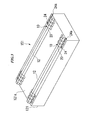
- FIG 3 is a perspective view showing the structure of the active face of the semiconductor device 151 where the terminals are formed.
- the semiconductor element 121 is, for example, an IC chip for activating the liquid crystal device.
- An electronic circuit an integrated circuit which has a plurality of electron devices such as thin-film transistors and wiring which connects each electron device is formed on an active face of the semiconductor element 121 (not shown in FIG. 3).
- a plurality of electrode pads 24 are arranged in a line along the longer side of the active face 121a.
- the electrode pads 24 protrude from the above-described electron devices, and function as outer electrodes of the electronic circuit.
- a resin bump 12 is formed straight along the electrode pad line 24a.
- a plurality of conductive layers 20 are formed from the surface of each electrode pad 24 over the surface of the resin bump 12. Bump electrodes 10 consist of the resin bump 12 and each conductive layer 20 arranged on the resin bump 12.
- FIGS 4A and 4B are drawings of the main part of the resin bump electrode 10.
- FIG. 4A is an enlarged plan view around the resin bump electrodes 10, and
- FIG 4B is a side sectional drawing along line A-A in FIG. 4A.
- the plurality of electrode pads 24 made of aluminum or other conducting material are arranged in a line around the edge of the active face 121 a of the semiconductor element 121.
- a passivation layer 26 made of SiN or other electric insulating material is formed over the entire active face 121 a of the semiconductor element 121, except for an aperture which is formed on each electrode pad 24.
- the resin bump 12 is formed on the passivation layer 26, to the inside of the electrode pad line 24a.
- the resin bump 12 is a straight bump arranged along the electrode pad line 24a.
- the resin bump 12 is made of polyimide resin, acrylic resin, phenol resin, epoxy resin, silicone resin, modified polyimide resin or other elastic resin materials. It is desirable that the resin bump 12 be shaped as a trapezoid or half-cylinder since this provides easy for elastic deformation in the cross-sectional surface. This enables the resin bump electrode 10 to perform elastic deformation easily when the resin bump electrode 10 is joined to the board 111, and contributes to improving the reliability of the conductive connection between the resin bump electrode 10 and the board.
- the plurality of conductive layers 20 are formed from the surface of each electrode pad 24 over the surface of the resin bump 12.
- the conductive layer 20 is made of Au, TiW, Cu, Ni, Pd, Al, Cr, Ti, W, NiV, Pb-free solder or other conducting materials.
- the conductive layer 20 is conductively connected to the electrode pad 24 via a seed layer 25 arranged on the active face 121 a of the semiconductor element 121.
- the seed layer 25 is provided on either side of the resin bump 12 and is formed as follows: a conducting material such as TiW is formed on the entire active face 121 a, and the conducting material on the surface of the resin bump 12 is selectively etched with an iodate solution which includes potassium iodide.
- the conductive layer 20 is formed by plating on the surface of the seed layer 25, and the removal of the seed layer 25 is carried out after the formation of the conductive layer 20.
- a space G is formed between the conductive layer 20 and the resin bump 12 by removing the seed layer 25.
- the seed layer 25 on the bump surface 12a is formed as a sacrifice layer to form the space G under the conductive layer 20. By removing the sacrifice layer, the conductive layer 20 and the resin bump 12 have no adhesion.
- the conductive layer 20 is formed from the electrode pad 24 to the other side of the resin bump 12, and joins the active face 121a.
- the conductive layer 20 joins the surface of the electrode pad 24 to the outside of the resin bump 12, being formed to the active face 121 a to the inside of the resin bump 12 over the surface of the resin bump 12, and joins the seed layer 25 or the passivation layer 26 on the active face 121 a to the inside of the resin bump 12. Because the conductive layer 20 is fixed to the active face 121 a, on either side of the resin bump 12, although it is not fixed on the resin bump 12, it is hard for the conductive layer 20 to be removed when joining to the board.
- the resin bump electrode 10 is compressed by thermocompression to the terminal 111bx on the board 111 with the sealing resin 122.
- the sealing resin 122 is a thermosetting resin, and is in a non-hardened or half-hardened state before mounting. In a case where the sealing resin 122 is in the non-hardened state, it is applied to the surface of the active face of the semiconductor element 121 (the underside in FIG. 1) or the surface of the board 111 before mounting. In a case where the sealing resin 122 is in the half-hardened state, it is inserted between the semiconductor device 151 and the board 111 as a film or a sheet. Epoxy resin is generally used as the sealing resin 122. Other resins may be used as long as the purpose is achieved.
- the mounting of the semiconductor device 151 is carried out by pressurizing the semiconductor device 151 onto the board 111 while heating with a hot-press head which is not shown in FIG 1.
- the sealing resin 122 is softened by heating, and the top of the resin bump electrode 10 is conductively connected to the terminal 111bx, pushing aside the softened resin.
- the resin bump 12 is elastically deformed in the connecting direction (the vertical direction in FIG 1) by pressurizing. In this condition; continuous heating causes the sealing resin 122 to bridge and harden, and the resin bump electrode 10 maintains the elastic deformation by the sealing resin 122, connecting conductively to the terminal 111bx even after releasing the pressurization.
- FIGS 5A through 5D are process drawings showing an example of the manufacturing method of the semiconductor device 151.
- a photosensitive resin is applied by a spin-coat method over the active face 121a of the semiconductor element 121 where the electrode pad 24 and the passivation layer 26 are formed.
- the resin is hardened by calcination at a high temperature.
- the resin bump 12 is formed to the inside of the electrode pad line 24a, along the length of the electrode pad line 24a. It is desirable that the resin bump 12 be shaped as a trapezoid or half-cylinder in its cross-sectional surface by a photo lithography process using a gray mask so as to allow easy elastic deformation.
- a conducting material 251 is formed as a sacrifice layer over the active face 121 a of the semiconductor element 121 by vapor deposition or sputtering. Photoresist is applied on the sacrifice layer and apertures of the conductive layer pattern are formed on the photoresist.
- a metal plating layer such as Au plating forming the conductive layer 20 is deposited on the apertures by an electrolytic plating method while the conducting material 251 is used as the seed layer.
- the thickness of the conductive layer 20 can be made 2 or 3 micrometers by the electrolytic plating method even though the thickness of the conducting material 251 formed by sputtering is 0.3 micrometers. Therefore, the conducting material 251 can be etched while the conductive layer 20 remains. This also contributes to preventing breaking or removal of the conductive layer 20 when the semiconductor device 151 is joined to the board 111. The resistance of the conductive layer 20 can also be reduced.
- the resist is removed, and the conducting material 251 is etched while the deposited metal plating layer (the conductive layer 20) is used as a mask.
- the etching rate depends on the surface condition of the board (such as the materials consisting the surface). For example, in a case where a resin bump made of an epoxy resin is formed on the board made of a silicon resin and TiW is plated thereon, the TiW plated on the resin bump is etched faster than the TiW plated on the silicon board by etching with hydrogen peroxide. This makes it possible to remove all of the TiW plated on the resin bump in a single etching process while a part of the TiW remains plated on the silicon board. Such a difference in the etching rate appears when other materials are used.
- the resin bump is made of polyimide resin, acrylic resin, phenol resin, epoxy resin, silicone resin, modified polyimide resin or other elastic resin materials and the passivation layer 26 is made of inorganic materials, except SiN, such as SiO 2 , etching proceeds faster on the resin bump.
- a metallic material, except TiW, such as Ti is used as the conducting material 251
- an etching fluid other than hydrogen peroxide such as a solution of potassium iodide and iodine acid is used.
- the conducting material 251 on the resin bump 12 is selectively removed while the conducting material 251 on the passivation layer 26 (that is, on the active face 121a) remains, utilizing the above-described difference in etching rate.
- the space G shown in FIG. 5D is formed between the conductive layer 20 and the resin bump 12, and the conductive layer 20 and the resin bump 12 are arranged without adhesion. If the etching rate of the surface of the resin bump 12a is not high enough for the process, only the seed layer 25 on the resin bump is etched while another part except for the resin bump is masked by photoresist or other substances.
- the resin bump electrode 10 may be separated by cutting the resin bump 12 in accordance with each electrode pad 24 after the plurality of conductive layers 20 are formed. Specifically, portions of the resin bump 12 without the conductive layer 20 (between each conductive layer 20) are removed by plasma etching using O 2 gas. Because the conductive layer 20 made of the metallic material is difficult to dry-etch compared with the resin material, the resin bump 12 without the conductive layer 20 can be selectively removed. Each conductive layer 20 may be formed on the single straight resin bump 12, but in a case where the resin bump is divided for each conductive layer 20, the effect of heat expansion or deformation of the resin bump 12 on each conductive layer 20 when the semiconductor device 151 is joined to the board 111 can be minimized.
- the space G is formed on the resin bump electrode 10 between the conductive layer 20 and the resin bump 12 in this embodiment, and the space G means there is no adhesion between the conductive layer 20 and the resin bump 12.
- This structure in conjunction with the resin bump 12, prevents the conductive layer 20 from elongation, shortening, and deforming when the semiconductor device 151 is joined to the board 111.
- the conductive layer 20 receives less stress than when it is joined to the resin bump making it hard to break.
- the conductive layer 20 and the resin bump 12 have no adhesion, the conductive layer 20 on the resin bump 12 has no support in a case in which the formation of the conductive layer 20 is ended on the resin bump 12.
- the portion of the conductive layer 20 without support has a possibility of being removed by deformation in joining or other stress.
- the conductive layer 20 is formed over the entire resin bump 12, and the conductive layer 20 joins the active face 121a. Therefore, both sides of the conductive layer 20 across the resin bump 12 (the side fixed to the electrode pad 24 and the side joined at the active face 121 a across the resin bump 12) can be securely fixed on the active face 121a. The above-described removal can be prevented with such a structure.
- FIG. 6 is a drawing showing the main portion of the resin bump electrode 10 of the embodiment This drawing corresponds to FIG 4B in the first embodiment.
- the electrode pad, the resin bump, and the passivation layer and several other components in this embodiment have the same structure and arrangement as the first embodiment. Therefore, the same reference number is provided to these common components and portions, and a detailed explanation is omitted.
- a plurality of conductive layers 22 is formed from the surface of the electrode pad 24 to the surface of the resin bump 12.
- a barrier metal layer 27 is provided between the conductive layer 22 and the electrode pad 24 so that the metal of the conductive layer 22 does not expand to the electrode pad 24.
- the barrier metal layer 27 is provided on either side of the resin bump 12.
- the conductive layer 22 is formed by vapor deposition or sputtering of a noble metal such as Au or Cu. Because these noble metals are chemically stable, they react very little with water or oxygen in a resin. For example, Au does usually not generate any oxide, and Cu oxide is chemically unstable although it is generated.
- the adhesion between the conductive layer 22 and the resin bump 12 is strengthened by the chemical reaction caused by water or oxygen in the resin (oxidative reaction). But because the conductive layer 22 is made of a noble metal such as Au or Cu in the embodiment, no chemical reactions occur at the interface between the conductive layer 22 and the resin bump 12. Therefore, the conductive layer 22 and the resin bump 12 have weakened adhe
- the conductive layer 22 is formed from the electrode pad 24 to the other side across the resin bump 12, and joins the active face 121 a. That is, the conductive layer 22 joins the surface of the electrode pad 24, outside the resin bump 12, and is formed to the active face 121 a, inside the resin bump 12, across the surface of the resin bump 12.
- the conductive layer 22 joins the barrier metal layer 27 or the passivation layer 26 provided on the active face 121a.
- the conductive layer 22 has no support on the resin bump 12, but because both sides of the conductive layer 22 across the resin bump 12 are fixed on the active face 121 a, it is hard to be removed when joining the board 111.
- the conductive layer 22 and the resin bump 12 have weakened adhesion in this embodiment, it makes it possible to reduce the effect of expansion or deformation of the resin bump 12 when joining with heat, and to reduce breaking of the conductive layer 22.
- the conductive layer 22 is made of a noble metal which is chemically stable, this embodiment makes it possible to form the conductive layer 22 on the resin bump 12 which has weakened adhesion by only plating a noble metal without the processes of forming and removing the seed layer 25 shown in the first embodiment. Therefore, it is possible to simplify the manufacturing process.
- FIG. 7 is a perspective view of an example of an electronic device according to an embodiment of the present invention.
- a mobile phone 1300 shown in FIG. 7 has the above-described electro-optic device as a small-sized display 1301. It also has a plurality of operating buttons 1302, an ear piece 1303 and a mouthpiece 1304.
- the above-described electro-optic device can be used as the image displaying device for not only mobile phones, but also electronic books, personal computers, digital still cameras, liquid crystal television sets, videotape recorders of view-finder type or direct monitor-view type, car navigation devices, pagers, electronic notepads, electronic calculators, word processors, workstations, videophones, point-of sale terminals, and devices with touch sensitive panels. This makes it possible to provide the electronic devices with better reliability in their conductive connection in every case listed above.
Landscapes
- Physics & Mathematics (AREA)
- Nonlinear Science (AREA)
- Mathematical Physics (AREA)
- Chemical & Material Sciences (AREA)
- Crystallography & Structural Chemistry (AREA)
- General Physics & Mathematics (AREA)
- Optics & Photonics (AREA)
- Wire Bonding (AREA)
- Internal Circuitry In Semiconductor Integrated Circuit Devices (AREA)
Abstract
Description
- The present invention relates to a semiconductor device and its manufacturing method, a circuit board, an electro-optic device and an electronic device.
- Priority is claimed on Japanese Patent Application No. 2004-313839, filed Oct. 28, 2004, the content of which is incorporated herein by reference.
- In circuit boards and liquid crystal displays which are used in various kinds of electric devices, semiconductor devices such as integrated circuit chips (IC chips) are mounted on the boards. For example, in a liquid crystal display, an IC chip for activating a liquid crystal panel is mounted on a glass board (the partner board) which is a component of the liquid crystal panel (a so-called COG structure). In a case in which an IC chip made of hard silicon board is mounted on a hard glass board, it is hard to absorb warpage of the IC chip and the glass board. To solve this problem, bump electrodes are formed on the IC chip, and the IC chip is mounted on the glass board by compressing the bump electrodes. This process enables the IC chip and the glass board to be conductively connected.
- Recently, terminals of IC chips are increasing in accordance with the high-definition of liquid crystal displays, and at the same time, downsizing of IC chips is eagerly demanded. To achieve this, narrowed pitches between bump electrodes formed on an IC chip are needed. Because an ordinary bump electrode is formed by carrying out electrolytic Au plating on an aperture of a plating resist, enlargement of the aspect ratio of the aperture is needed to narrow pitches between bump electrodes. Therefore, it is difficult to narrow pitches between bump electrodes.
- A
resin bump electrode 10 shown in FIG. 8 has been developed. Theresin bump electrode 10 is made by forming a conductinglayer 20 on aresin bump 12, and the conductinglayer 20 is connected to anelectrode pad 24 of an IC chip 21 (for example, refer to Japanese Unexamined Patent Application, First Publication No. H01-13734). Theresin bump electrode 10 makes elastic deformation by contacting a partner board, and the warpage of theIC chip 21 and the partner board can be absorbed. Since this process does not require enlargement of the aspect ratio of the aperture, it is easier to narrow pitches between bump electrodes than in an ordinary method. - However, because the
resin bump 12 has high coefficient of thermal expansion, when carrying out a hot press bond of theIC chip 21 and the partner board, theconductive layer 20 receives great tensile stress due to deforming following the expansion of theresin bump 12. - There are some cases in which sufficient reliability in the conductive connection is not obtained because of a breaking of the
conductive layer 20 by the deformation of theresin bump 12 which deforms due to absorbing the pressure of the bonding. - The present invention provides a semiconductor device including a semiconductor element, an electrode pad formed on the semiconductor element, and a bump electrode conductively connected to the electrode pad which includes a resin bump formed on an active face of the semiconductor element, and a conductive layer provided from the electrode pad to the surface of the resin bump, the conductive layer and the resin bump being arranged without adhesion. A material with high ductibility such as Au is suitable for the conductive layer.
- In the device, the conductive layer is free from elongation, shortening, and deforming in conjunction with the resin bump when the semiconductor device is joined to the board via the bump electrode. Therefore, the conductive layer receives less stress than when it is joined to the resin bump, and it becomes hard to break.
- In the semiconductor device of the present invention, a space may be formed between the conductive layer and the resin bump. This enables sure reduction of the adhesion strength.
- In the semiconductor device of the present invention, the conductive layer may be made of a metal which has weakened adhesion with the resin bump- More specifically, the conductive layer may be made of noble metal with weakened adhesion to the resin bump such as Au or Cu. Because noble metals are chemically stable, they react with water or oxygen in a resin very little. For example, Au usually does not generate any oxide, and Cu oxide is chemically unstable although it is generated. The adhesion between the conductive layer and the resin bump is strengthened by the chemical reaction caused by water or oxygen in the resin (oxidative reaction). But because the conductive layer is made of a chemically stable noble metal such as Au or Cu in the present invention, no chemical reactions occur at the interface between the conductive layer and the resin bump. Therefore, the conductive layer and the resin bump have weakened adhesion. Because processes to weaken the adhesion between the conductive layer and the resin bump are not needed, it is possible to simplify the manufacturing process.
- In the semiconductor device of the present invention, the conductive layer may be formed from the electrode pad to the other side across the resin bump, and join the active face at the other side.
- As explained, because the conductive layer is formed so that the conductive layer and the resin bump have no adhesion, the conductive layer on the resin bump has no support in a case in which the formation of the conductive layer is ended on the resin bump. The portion of the conductive layer without support has a possibility of being removed when the semiconductor device joins the board. In the present invention, the conductive layer is extended to the other side of the resin bump, and joins the active face. Therefore, both sides of the conductive layer across the resin bump (the side fixed to the electrode pad and the side joined the active face across the resin bump) can be securely fixed on the active face. The above-described removal can be prevented.
- In the semiconductor device of the present invention, a plurality of electrode pads may be provided in a line on the active face, and the resin bump may be formed straight along the line of the electrode pads, and the conductive layer may be formed from each electrode pad to the surface of the resin bump.
- Because the single straight resin bump is provided for the plurality of the electrode pads in this structure, it is possible to simplify the manufacturing process.
- The present invention provides a manufacturing method of a semiconductor device which has an electrode pad and a bump electrode conductively connected to the electrode pad on its active face, and the manufacturing method includes forming a resin bump on the semiconductor element and forming a conductive layer from the electrode pad to the surface of the resin bump without adhesion at the surface of the resin bump.
- Through the processes, the conductive layer is made to be free from elongation, shortening, and deforming in conjunction with the resin bump when the semiconductor device is joined to the board via the bump electrode. Therefore, the conductive layer receives less stress than when it is joined the resin bump, and it becomes hard to break.
- In the manufacturing method of the semiconductor device of the present invention, the conductive layer may be formed from the electrode pad to the other side across the resin bump, and may be joined to the active face at the other side.
- Because both sides of the conductive layer across the resin bump can be securely fixed, the conductive layer becomes hard to remove when the semiconductor device joins the board.
- In the manufacturing method of a semiconductor device of the present invention, the forming of the conductive layer may include forming a sacrifice layer between the conductive layer and the resin bump and forming a space between the conductive layer and the resin bump by removing the sacrifice layer on the resin bump. This enables sure reduction of the adhesion strength.
- In the manufacturing method of a semiconductor device of the present invention, the form of the space may include removing the sacrifice layer on the resin bump by etching utilizing the difference in etching rate between the surface of the active face and the surface of the resin bump while the sacrifice layer on the active face remains.
- The inventors of the present invention recognized that the etching rate depends on the surface condition of the board. For example, in a case that a resin bump made of epoxy resin is formed on the board made of silicone resin and TiW is plated on that, the TiW plated on the resin bump is etched faster than the TiW plated on the silicone board when etching with hydrogen peroxide. The present invention selectively removes the sacrifice layer, utilizing the difference in etching rate. Because the present invention needs only a single etching of the whole active face to form a space, it makes it possible to simplify the manufacturing process.
- The active face may be made of inorganic material. Because a bigger difference in the surface condition from the resin bump can be made, this makes it possible to carry out the etching more effectively.
- In the manufacturing method of a semiconductor device of the present invention, the conductive layer may be formed by plating while the sacrifice layer is used as a seed layer.
- Because the conductive layer becomes easy to make thicker, a breaking of the conductive layer when joining the active face can be prevented more certainly. The resistance of the conductive layer also can be reduced by thickening the conductive layer.
- In the manufacturing method of a semiconductor device of the present invention, the forming of the conductive layer may include forming a conductive layer without adhesion to the resin bump by evaporating or sputtering a noble metal.
- Because chemically stable materials such as noble metals are used as the conductive layer, no chemical reactions with the resin bump (such as oxidation by water or oxygen in the resin bump) occur. Therefore, the conductive layer and the resin bump have weakened adhesion. Because the conductive layer can be made without processes to form and remove the sacrifice layer, it is possible to simplify the manufacturing process.
- In the manufacturing method of a semiconductor device of the present invention, a plurality of the electrode pads may be provided in a line on the active face, and the resin bump may be formed straight along the line of the electrode pads, and the conductive layer may be formed from each electrode pad to the surface of the resin bump.
- Because the single straight resin bump is provided for the plurality of the electrode pads in this structure, it makes it possible to simplify the manufacturing process.
- In the manufacturing method of a semiconductor device of the present invention, cutting the resin bump and separating the bump electrode according to the electrode pads may be included.
- Because the resin bump is separated for each conductive layer, the effect of heat expansion or a deformation of the resin bump on each conductive layer when the semiconductor device joins the board can be minimized.
- The present invention provides a circuit board on which the semiconductor device of the present invention is mounted, and the semiconductor is conductively connected to the electrode terminal of the circuit board by the conductive layer arranged on the resin bump.
- A circuit board which has better reliability in its conductive connection can be provided by the present invention.
- In the circuit board of the present invention, the conductive layer contacts the circuit by elastic deformation of the resin bump and the semiconductor device and the electrode terminals may be supported by a sealing resin filled around the conductive connection of the semiconductor device and the electrode terminals.
- Because the conductive layer covers the resin bump in the electrode bump, it is easy to cause elastic deformation by pressing the electrode terminal onto the circuit board, and the elastic deformation of the bump electrode is maintained by a sealing resin filled around the conductive connection. The condition in which the circuit board and the bump electrode are joined with elastic deformation generates a reactive force (a pushing force) continually. This makes it possible to maintain the conductive connection and high reliability in the conductive connection can be obtained. Because this structure does not need any expensive materials such as an anisotropic conductive film or anisotropic conductive paste, this contributes to reduce cost for manufacturing.
- The present invention provides an electro-optic device which is equipped with the semiconductor device of the present invention or the circuit board of the present invention.
- The present invention provides an electronic device which is equipped with the circuit board of the present invention or the electro-optic device of the present invention.
- An electro-optic device or an electronic device with high reliability in its conductive connection can be provided by the present invention.
-
- FIG. 1 is a drawing of the liquid crystal display illustrating an embodiment of the electro-optic device.
- FIG. 2 is a drawing of the mounting structure of the semiconductor device in the liquid crystal display.
- FIG. 3 is a perspective view of the semiconductor device according to the first embodiment.
- FIG. 4A is an enlarged plan view around the resin bump electrodes of the semiconductor device of the first embodiment, and FIG. 4B is a side sectional view along line A-A in FIG. 4A.
- FIGs. 5A to 5D are process drawings to explain the manufacturing process of the semiconductor device of the first embodiment.
- FIG. 6 is an enlarged view of the electrodes of the semiconductor device according to a second embodiment.
- FIG. 7 is a perspective view of an example of an electronic device according to an embodiment of the present invention.
- FIG. 8 is a drawing of a conventional resin bump electrode (a prior art).
- An explanation of embodiments of the present invention is given, referring to the drawings. In the drawings, the thickness and the size of each component are not to scale for better explanation.
- FIG. 1 is a drawing of a liquid crystal display of an electro-optic device according to an embodiment of the present invention. A liquid
crystal display device 100 in FIG. 1 has aliquid crystal panel 110 and asemiconductor element 121 disposed thereon. A deflecting plate, a reflecting sheet, a backlight or other additional portions which are not shown in the drawing are provided as required. - The
liquid crystal panel 110 has aboard 111 and aboard 112 made of glass or plastic. Theboard 111 and theboard 112 are disposed opposite each other, and are adhered together by a seal which is not shown in the drawing. Liquid crystal made of an electro-optic material is included between theboard 111 and the board 112 (not shown in FIG. 1). Anelectrode 111 a made of a clear conductive material such as ITO (Indium Tin Oxide) is formed on the surface inside theboard 111, and anelectrode 112a which is faced perpendicularly to theelectrode 111 a is formed on the surface inside theboard 112. Theelectrode 111 a and theelectrode 112a extend out to a protrudingportion 111T, and electrode terminals 111bx and 111cx are formed at the terminal of each electrode, respectively.Input wiring 111d is formed near the terminal of the protrudingportion 111T, and a terminal 111 dx is formed at the inner edge of the protrudingportion 111T. - The
semiconductor element 121 is mounted on the protrudingportion 111T with a sealingresin 122. Thesemiconductor element 121 is, for example, an IC chip for activating theliquid crystal panel 110. A plurality of bump electrodes (not shown in FIG. 1) are formed on the underside of thesemiconductor element 121, and the bump electrodes are conductively connected to each terminal 111bx, 111cx and 111dx on the protrudingportion 111T. - A
flexible circuit board 123 is connected via an anisotropicconductive layer 124 to input terminals 111dy which are formed at the outer end ofinput wiring 111d. The input terminals 111dy are conductively connected to each wiring (not shown in FIG. 1) provided on theflexible circuit board 123. A control signal, a picture signal or potential of power or other external electric signals are provided to theinput wiring 111 dy via theflexible circuit board 123. Then, an activating signal to activate the liquid crystal is generated in thesemiconductor element 121 and provided to theliquid crystal panel 110. - The liquid
crystal display device 100 of this embodiment constructed in the above-described manner is able to carry out optical modulation by reorienting the liquid crystal pixels by applying a voltage between the perpendicularly placedelectrodes semiconductor element 121. Therefore, it is possible to form desired picture on a display region in theliquid crystal panel 110 where the pixels are arranged. - FIG. 2 is a side sectional view along line H-H in FIG. 1 showing the mounting structure of a
semiconductor device 151 in the liquidcrystal display device 100. As shown in FIG 2, a plurality ofresin bump electrodes 10 are provided on the active face (the underside in FIG. 2) as terminals of the IC chip. The tips of theresin bump electrodes 10 have a direct conductive connection to theterminals 111 bx and 111 dx of theboard 111. Ahardened sealing resin 122 made of a thermosetting resin surrounds the conductive connection between theresin bump electrodes 10 and theelectrodes 111 bx and 111 dx. - An explanation of the structure of the terminals of the
semiconductor device 151 is given. FIG 3 is a perspective view showing the structure of the active face of thesemiconductor device 151 where the terminals are formed. - The
semiconductor element 121 is, for example, an IC chip for activating the liquid crystal device. An electronic circuit (an integrated circuit) which has a plurality of electron devices such as thin-film transistors and wiring which connects each electron device is formed on an active face of the semiconductor element 121 (not shown in FIG. 3). In thesemiconductor element 121 shown in FIG. 3, a plurality ofelectrode pads 24 are arranged in a line along the longer side of theactive face 121a. Theelectrode pads 24 protrude from the above-described electron devices, and function as outer electrodes of the electronic circuit. To the inside of theelectrode pad line 24a on theactive face 121 a, aresin bump 12 is formed straight along theelectrode pad line 24a. A plurality ofconductive layers 20 are formed from the surface of eachelectrode pad 24 over the surface of theresin bump 12.Bump electrodes 10 consist of theresin bump 12 and eachconductive layer 20 arranged on theresin bump 12. - FIGS 4A and 4B are drawings of the main part of the
resin bump electrode 10. FIG. 4A is an enlarged plan view around theresin bump electrodes 10, and FIG 4B is a side sectional drawing along line A-A in FIG. 4A. As shown in FIGS 4A and 4B, the plurality ofelectrode pads 24 made of aluminum or other conducting material are arranged in a line around the edge of theactive face 121 a of thesemiconductor element 121. Apassivation layer 26 made of SiN or other electric insulating material is formed over the entireactive face 121 a of thesemiconductor element 121, except for an aperture which is formed on eachelectrode pad 24. - The
resin bump 12 is formed on thepassivation layer 26, to the inside of theelectrode pad line 24a. Theresin bump 12 is a straight bump arranged along theelectrode pad line 24a. Theresin bump 12 is made of polyimide resin, acrylic resin, phenol resin, epoxy resin, silicone resin, modified polyimide resin or other elastic resin materials. It is desirable that theresin bump 12 be shaped as a trapezoid or half-cylinder since this provides easy for elastic deformation in the cross-sectional surface. This enables theresin bump electrode 10 to perform elastic deformation easily when theresin bump electrode 10 is joined to theboard 111, and contributes to improving the reliability of the conductive connection between theresin bump electrode 10 and the board. - The plurality of
conductive layers 20 are formed from the surface of eachelectrode pad 24 over the surface of theresin bump 12. Theconductive layer 20 is made of Au, TiW, Cu, Ni, Pd, Al, Cr, Ti, W, NiV, Pb-free solder or other conducting materials. Theconductive layer 20 is conductively connected to theelectrode pad 24 via aseed layer 25 arranged on theactive face 121 a of thesemiconductor element 121. Theseed layer 25 is provided on either side of theresin bump 12 and is formed as follows: a conducting material such as TiW is formed on the entireactive face 121 a, and the conducting material on the surface of theresin bump 12 is selectively etched with an iodate solution which includes potassium iodide. Theconductive layer 20 is formed by plating on the surface of theseed layer 25, and the removal of theseed layer 25 is carried out after the formation of theconductive layer 20. Thus, a space G is formed between theconductive layer 20 and theresin bump 12 by removing theseed layer 25. In other words, theseed layer 25 on thebump surface 12a is formed as a sacrifice layer to form the space G under theconductive layer 20. By removing the sacrifice layer, theconductive layer 20 and theresin bump 12 have no adhesion. - The
conductive layer 20 is formed from theelectrode pad 24 to the other side of theresin bump 12, and joins theactive face 121a. Thus, theconductive layer 20 joins the surface of theelectrode pad 24 to the outside of theresin bump 12, being formed to theactive face 121 a to the inside of theresin bump 12 over the surface of theresin bump 12, and joins theseed layer 25 or thepassivation layer 26 on theactive face 121 a to the inside of theresin bump 12. Because theconductive layer 20 is fixed to theactive face 121 a, on either side of theresin bump 12, although it is not fixed on theresin bump 12, it is hard for theconductive layer 20 to be removed when joining to the board. - In FIG. 2, the
resin bump electrode 10 is compressed by thermocompression to the terminal 111bx on theboard 111 with the sealingresin 122. The sealingresin 122 is a thermosetting resin, and is in a non-hardened or half-hardened state before mounting. In a case where the sealingresin 122 is in the non-hardened state, it is applied to the surface of the active face of the semiconductor element 121 (the underside in FIG. 1) or the surface of theboard 111 before mounting. In a case where the sealingresin 122 is in the half-hardened state, it is inserted between thesemiconductor device 151 and theboard 111 as a film or a sheet. Epoxy resin is generally used as the sealingresin 122. Other resins may be used as long as the purpose is achieved. - The mounting of the
semiconductor device 151 is carried out by pressurizing thesemiconductor device 151 onto theboard 111 while heating with a hot-press head which is not shown in FIG 1. During the process, the sealingresin 122 is softened by heating, and the top of theresin bump electrode 10 is conductively connected to the terminal 111bx, pushing aside the softened resin. Theresin bump 12 is elastically deformed in the connecting direction (the vertical direction in FIG 1) by pressurizing. In this condition; continuous heating causes the sealingresin 122 to bridge and harden, and theresin bump electrode 10 maintains the elastic deformation by the sealingresin 122, connecting conductively to the terminal 111bx even after releasing the pressurization. - An explanation of the method for manufacturing the semiconductor device according to an embodiment of the present invention is given. FIGS 5A through 5D are process drawings showing an example of the manufacturing method of the
semiconductor device 151. - In this embodiment, as shown in FIG 5A, a photosensitive resin is applied by a spin-coat method over the
active face 121a of thesemiconductor element 121 where theelectrode pad 24 and thepassivation layer 26 are formed. After ultraviolet ray exposure using a glass mask and developing with developing fluid, the resin is hardened by calcination at a high temperature. By these processes, theresin bump 12 is formed to the inside of theelectrode pad line 24a, along the length of theelectrode pad line 24a. It is desirable that theresin bump 12 be shaped as a trapezoid or half-cylinder in its cross-sectional surface by a photo lithography process using a gray mask so as to allow easy elastic deformation. - As shown in FIG. 5B, a conducting
material 251 is formed as a sacrifice layer over theactive face 121 a of thesemiconductor element 121 by vapor deposition or sputtering. Photoresist is applied on the sacrifice layer and apertures of the conductive layer pattern are formed on the photoresist. As shown in FIG. 5C, a metal plating layer such as Au plating forming theconductive layer 20 is deposited on the apertures by an electrolytic plating method while the conductingmaterial 251 is used as the seed layer. By using the plating method, it is easy to make theconductive layer 20 become thicker, and contributes to the improving the reliability of theconductive layer 20. For example, the thickness of theconductive layer 20 can be made 2 or 3 micrometers by the electrolytic plating method even though the thickness of the conductingmaterial 251 formed by sputtering is 0.3 micrometers. Therefore, the conductingmaterial 251 can be etched while theconductive layer 20 remains. This also contributes to preventing breaking or removal of theconductive layer 20 when thesemiconductor device 151 is joined to theboard 111. The resistance of theconductive layer 20 can also be reduced. - Then the resist is removed, and the conducting
material 251 is etched while the deposited metal plating layer (the conductive layer 20) is used as a mask. - The inventors of the present invention recognized that the etching rate depends on the surface condition of the board (such as the materials consisting the surface). For example, in a case where a resin bump made of an epoxy resin is formed on the board made of a silicon resin and TiW is plated thereon, the TiW plated on the resin bump is etched faster than the TiW plated on the silicon board by etching with hydrogen peroxide. This makes it possible to remove all of the TiW plated on the resin bump in a single etching process while a part of the TiW remains plated on the silicon board. Such a difference in the etching rate appears when other materials are used. For example, when the resin bump is made of polyimide resin, acrylic resin, phenol resin, epoxy resin, silicone resin, modified polyimide resin or other elastic resin materials and the
passivation layer 26 is made of inorganic materials, except SiN, such as SiO2, etching proceeds faster on the resin bump. The same effect is obtained when a metallic material, except TiW, such as Ti is used as the conductingmaterial 251, and when an etching fluid other than hydrogen peroxide such as a solution of potassium iodide and iodine acid is used. - In this embodiment, the conducting
material 251 on theresin bump 12 is selectively removed while the conductingmaterial 251 on the passivation layer 26 (that is, on theactive face 121a) remains, utilizing the above-described difference in etching rate. - When a wet etching is carried out after laminating with the conducting
material 251 and theconductive layer 20, the side etching of the conductingmaterial 251 on the surface of theresin bump 12a becomes much larger than that of the conductingmaterial 251 on thepassivation layer 26 for the aforementioned reason. Then all of the conductingmaterial 251 between theresin bump 12 and theconductive layer 20 is etched while a part of the conductingmaterial 251 between thepassivation layer 26 and theconductive layer 20 remains. - Through these processes, the space G shown in FIG. 5D is formed between the
conductive layer 20 and theresin bump 12, and theconductive layer 20 and theresin bump 12 are arranged without adhesion. If the etching rate of the surface of theresin bump 12a is not high enough for the process, only theseed layer 25 on the resin bump is etched while another part except for the resin bump is masked by photoresist or other substances. - The
resin bump electrode 10 may be separated by cutting theresin bump 12 in accordance with eachelectrode pad 24 after the plurality ofconductive layers 20 are formed. Specifically, portions of theresin bump 12 without the conductive layer 20 (between each conductive layer 20) are removed by plasma etching using O2 gas. Because theconductive layer 20 made of the metallic material is difficult to dry-etch compared with the resin material, theresin bump 12 without theconductive layer 20 can be selectively removed. Eachconductive layer 20 may be formed on the singlestraight resin bump 12, but in a case where the resin bump is divided for eachconductive layer 20, the effect of heat expansion or deformation of theresin bump 12 on eachconductive layer 20 when thesemiconductor device 151 is joined to theboard 111 can be minimized. - As explained, the space G is formed on the
resin bump electrode 10 between theconductive layer 20 and theresin bump 12 in this embodiment, and the space G means there is no adhesion between theconductive layer 20 and theresin bump 12. This structure, in conjunction with theresin bump 12, prevents theconductive layer 20 from elongation, shortening, and deforming when thesemiconductor device 151 is joined to theboard 111. Theconductive layer 20 receives less stress than when it is joined to the resin bump making it hard to break. - With this structure, because the
conductive layer 20 and theresin bump 12 have no adhesion, theconductive layer 20 on theresin bump 12 has no support in a case in which the formation of theconductive layer 20 is ended on theresin bump 12. The portion of theconductive layer 20 without support has a possibility of being removed by deformation in joining or other stress. In the embodiment, theconductive layer 20 is formed over theentire resin bump 12, and theconductive layer 20 joins theactive face 121a. Therefore, both sides of theconductive layer 20 across the resin bump 12 (the side fixed to theelectrode pad 24 and the side joined at theactive face 121 a across the resin bump 12) can be securely fixed on theactive face 121a. The above-described removal can be prevented with such a structure. - An explanation on the second embodiment of the present invention is given. FIG. 6 is a drawing showing the main portion of the
resin bump electrode 10 of the embodiment This drawing corresponds to FIG 4B in the first embodiment. - The electrode pad, the resin bump, and the passivation layer and several other components in this embodiment have the same structure and arrangement as the first embodiment. Therefore, the same reference number is provided to these common components and portions, and a detailed explanation is omitted.
- In this embodiment, a plurality of
conductive layers 22 is formed from the surface of theelectrode pad 24 to the surface of theresin bump 12. Abarrier metal layer 27 is provided between theconductive layer 22 and theelectrode pad 24 so that the metal of theconductive layer 22 does not expand to theelectrode pad 24. Thebarrier metal layer 27 is provided on either side of theresin bump 12. Theconductive layer 22 is formed by vapor deposition or sputtering of a noble metal such as Au or Cu. Because these noble metals are chemically stable, they react very little with water or oxygen in a resin. For example, Au does usually not generate any oxide, and Cu oxide is chemically unstable although it is generated. The adhesion between theconductive layer 22 and theresin bump 12 is strengthened by the chemical reaction caused by water or oxygen in the resin (oxidative reaction). But because theconductive layer 22 is made of a noble metal such as Au or Cu in the embodiment, no chemical reactions occur at the interface between theconductive layer 22 and theresin bump 12. Therefore, theconductive layer 22 and theresin bump 12 have weakened adhesion. - The
conductive layer 22 is formed from theelectrode pad 24 to the other side across theresin bump 12, and joins theactive face 121 a. That is, theconductive layer 22 joins the surface of theelectrode pad 24, outside theresin bump 12, and is formed to theactive face 121 a, inside theresin bump 12, across the surface of theresin bump 12. Theconductive layer 22 joins thebarrier metal layer 27 or thepassivation layer 26 provided on theactive face 121a. Theconductive layer 22 has no support on theresin bump 12, but because both sides of theconductive layer 22 across theresin bump 12 are fixed on theactive face 121 a, it is hard to be removed when joining theboard 111. - As explained, since the
conductive layer 22 and theresin bump 12 have weakened adhesion in this embodiment, it makes it possible to reduce the effect of expansion or deformation of theresin bump 12 when joining with heat, and to reduce breaking of theconductive layer 22. - Because the
conductive layer 22 is made of a noble metal which is chemically stable, this embodiment makes it possible to form theconductive layer 22 on theresin bump 12 which has weakened adhesion by only plating a noble metal without the processes of forming and removing theseed layer 25 shown in the first embodiment. Therefore, it is possible to simplify the manufacturing process. - An explanation of an electronic device which is equipped with the above-described electro-optic device or the semiconductor device is given. FIG. 7 is a perspective view of an example of an electronic device according to an embodiment of the present invention. A
mobile phone 1300 shown in FIG. 7 has the above-described electro-optic device as a small-sized display 1301. It also has a plurality ofoperating buttons 1302, anear piece 1303 and amouthpiece 1304. - The above-described electro-optic device can be used as the image displaying device for not only mobile phones, but also electronic books, personal computers, digital still cameras, liquid crystal television sets, videotape recorders of view-finder type or direct monitor-view type, car navigation devices, pagers, electronic notepads, electronic calculators, word processors, workstations, videophones, point-of sale terminals, and devices with touch sensitive panels. This makes it possible to provide the electronic devices with better reliability in their conductive connection in every case listed above.
- While preferred embodiments of the invention have been described and illustrated above, it should be understood that these are exemplary of the invention and are not to be considered as limiting. Additions, omissions, substitutions, and other modifications can be made without departing from the spirit or scope of the present invention. Accordingly, the invention is not to be considered as being limited by the foregoing description, and is only limited by the scope of the appended claims.
Claims (21)
- A semiconductor device comprising:a semiconductor element (121);an electrode pad (24) formed on the semiconductor element (121); anda bump electrode (10) conductively connected to the electrode pad (24) comprising:a resin bump (12) formed on an active face (121 a) of the semiconductor element (121); anda conductive layer (20) provided from the electrode pad (24) to the surface of the resin bump (12), the conductive layer (20) and the resin bump (12) being arranged without adhesion.
- The semiconductor device according to claim 1, wherein a space (G) is formed between the conductive layer (20) and the resin bump (12).
- The semiconductor device according to claim 1, wherein the conductive layer (20) is made of a metal which has weakened adhesion with the resin bump (12).
- The semiconductor device according to claim 3, wherein the conductive layer (20) is made of a noble metal which has weakened adhesion with the resin bump (12).
- The semiconductor device according to claim 3, wherein the conductive layer (20) is made of Au or Cu.
- The semiconductor device according to any one of claims 1 to 5, wherein the conductive layer (20) is formed from the electrode pad (24) to the other side across the resin bump (12), and joins the active face (121a) on the other side.
- The semiconductor device according to any one of claims I to 6, further comprising:an electrode pad line (24a) along which a plurality of the electrode pads (24) are arranged in a line on the active face (121a), wherein the resin bump (12) is formed straight along the electrode pad line (24a), and the conductive layer (20) is formed from each electrode pad (24) to the surface of the resin bump (12).
- A manufacturing method for a semiconductor device which has an electrode pad (24) and a bump electrode (10) conductively connected to the electrode pad (24) on its active face (121a), the manufacturing method comprising:forming a resin bump (12) on a semiconductor element (121); andforming a conductive layer (20) from the electrode pad (24) to the surface of the resin bump (12) without adhesion at the surface of the resin bump (12).
- A manufacturing method for a semiconductor device according to claim 8, wherein the conductive layer (20) is formed from the electrode pad (24) to the other side across the resin bump (12), and is joined to the active face (121a) at both ends across the resin bump (12).
- A manufacturing method for a semiconductor device according to claim 8 or 9, wherein the forming of the conductive layer (20) further comprising:forming a sacrifice layer between the conductive layer (20) and the resin bump (12); andforming a space (G) between the conductive layer (20) and the resin bump (12) by removing the sacrifice layer on the resin bump (12).
- A manufacturing method for a semiconductor device according to claim 10, wherein the sacrifice layer on the surface of the resin bump (12) is removed in the step of forming the space (G) by etching utilizing the difference in etching rate between the surface of the active face (121a) and the surface of the resin bump (12) while the sacrifice layer on the surface of the active face (121a) remains.
- A manufacturing method for a semiconductor device according to claim 11, wherein the active face (121a) is made of an inorganic material.
- A manufacturing method for a semiconductor device according to any one of claims 10 to 12, wherein the conductive layer (20) is formed by plating while the sacrifice layer is used as a seed layer.
- A manufacturing method for a semiconductor device according to claim 8 or 9, wherein the step of forming the conductive layer (20) includes vapor deposition or sputtering of a noble metal.
- A manufacturing method for a semiconductor device according to claim 14, wherein the conductive layer (20) is made of Au or Cu.
- A manufacturing method for a semiconductor device according to any one of claims 8 to 15, wherein a plurality of the electrode pads (24) are arranged in a line on the active face (121a) and the step of forming the resin bump (12) is carried out so that the resin bump (12) is straight along the line of electrode pads (24), and the step of forming the conductive layer (20) is carried out so that the conductive layer (20) is formed from each electrode pad (24) to the surface of the resin bump (12).
- A manufacturing method for a semiconductor device according to claim 16, wherein the resin bump (12) is cut and the bump electrode (10) is separated according to each electrode pad (24).
- A circuit board on which a semiconductor device (151) according to any one of claims 1 to 7 is mounted, wherein the semiconductor device (151) is conductively connected to electrode terminals (111bx, 111cx, 111dx) of a circuit board by a conductive layer (20) formed on a resin bump (12).
- A circuit board according to claim 18, wherein the conductive layer (20) joins the circuit by elastic deformation of the resin bump (12) and the semiconductor device (151) and the electrode terminals (111bx, 111ex, 111dx) are supported by a sealing resin surrounding the conductive connection of the semiconductor device (151) and the electrode terminals (111 bx, 111 cx, 111 dx).
- An electro-optic device which is equipped with a semiconductor device (151) according to any one of claims 1 to 7 or a circuit board according to claim 18 or 19.
- An electronic device which is equipped with the circuit board according to claim 18 or 19, or an electro-optic device according to claim 20.
Applications Claiming Priority (1)
| Application Number | Priority Date | Filing Date | Title |
|---|---|---|---|
| JP2004313839A JP4165495B2 (en) | 2004-10-28 | 2004-10-28 | Semiconductor device, semiconductor device manufacturing method, circuit board, electro-optical device, electronic device |
Publications (2)
| Publication Number | Publication Date |
|---|---|
| EP1653503A2 true EP1653503A2 (en) | 2006-05-03 |
| EP1653503A3 EP1653503A3 (en) | 2012-04-18 |
Family
ID=35705278
Family Applications (1)
| Application Number | Title | Priority Date | Filing Date |
|---|---|---|---|
| EP05023273A Withdrawn EP1653503A3 (en) | 2004-10-28 | 2005-10-25 | Semiconductor device, circuit board, electro-optic device, electronic device |
Country Status (6)
| Country | Link |
|---|---|
| US (1) | US7375427B2 (en) |
| EP (1) | EP1653503A3 (en) |
| JP (1) | JP4165495B2 (en) |
| KR (1) | KR100754575B1 (en) |
| CN (1) | CN100424862C (en) |
| TW (1) | TWI277159B (en) |
Families Citing this family (19)
| Publication number | Priority date | Publication date | Assignee | Title |
|---|---|---|---|---|
| US7960830B2 (en) * | 2003-11-14 | 2011-06-14 | Industrial Technology Research Institute | Electronic assembly having a multilayer adhesive structure |
| US8604613B2 (en) * | 2003-11-14 | 2013-12-10 | Industrial Technology Research Institute | Electronic assembly having a multilayer adhesive structure |
| JP4269173B2 (en) | 2005-07-06 | 2009-05-27 | セイコーエプソン株式会社 | Semiconductor device and manufacturing method thereof |
| JP2007214164A (en) * | 2006-02-07 | 2007-08-23 | Epson Imaging Devices Corp | ELECTRO-OPTICAL DEVICE, SEMICONDUCTOR DEVICE, ELECTRO-OPTICAL DEVICE MANUFACTURING METHOD, AND ELECTRONIC DEVICE |
| JP2007258518A (en) * | 2006-03-24 | 2007-10-04 | Epson Imaging Devices Corp | Semiconductor device, electro-optical device and electronic apparatus |
| JP4920330B2 (en) * | 2006-07-18 | 2012-04-18 | ソニー株式会社 | Mounting method for mounting structure, mounting method for light emitting diode display, mounting method for light emitting diode backlight, and mounting method for electronic device |
| JP4862529B2 (en) * | 2006-07-21 | 2012-01-25 | 株式会社セガ | Game machine, game processing method, and storage medium storing program |
| JP4273356B2 (en) | 2007-02-21 | 2009-06-03 | セイコーエプソン株式会社 | Manufacturing method of semiconductor device |
| JP4548459B2 (en) | 2007-08-21 | 2010-09-22 | セイコーエプソン株式会社 | Electronic component mounting structure |
| JP5169071B2 (en) * | 2007-08-21 | 2013-03-27 | セイコーエプソン株式会社 | Electronic component, electronic device, mounting structure for electronic component, and method for manufacturing mounting structure for electronic component |
| JP4535295B2 (en) * | 2008-03-03 | 2010-09-01 | セイコーエプソン株式会社 | Semiconductor module and manufacturing method thereof |
| CN101866899A (en) * | 2009-04-20 | 2010-10-20 | 奇景光电股份有限公司 | Semiconductor device with a plurality of semiconductor chips |
| JP2011061035A (en) * | 2009-09-10 | 2011-03-24 | Renesas Electronics Corp | Method of manufacturing semiconductor device, and mask |
| JP5685807B2 (en) * | 2009-12-03 | 2015-03-18 | 富士通株式会社 | Electronic equipment |
| KR20130030494A (en) * | 2011-09-19 | 2013-03-27 | 삼성전기주식회사 | Plating pattern and method of manufacturing the same |
| KR102540850B1 (en) * | 2016-07-29 | 2023-06-07 | 삼성디스플레이 주식회사 | Integrated circuit chip and display device comprising the same |
| KR101897653B1 (en) * | 2017-03-06 | 2018-09-12 | 엘비세미콘 주식회사 | Methods of fabricating compliant bump |
| CN110164830B (en) * | 2019-04-26 | 2021-02-05 | 厦门云天半导体科技有限公司 | A three-dimensional interconnection structure of a power device and a manufacturing method thereof |
| TWI799226B (en) * | 2022-04-07 | 2023-04-11 | 頎邦科技股份有限公司 | Chip-on-film package |
Family Cites Families (8)
| Publication number | Priority date | Publication date | Assignee | Title |
|---|---|---|---|---|
| JPH0621257Y2 (en) | 1987-07-16 | 1994-06-01 | 三洋電機株式会社 | Solid-state imaging device |
| JP2833326B2 (en) * | 1992-03-03 | 1998-12-09 | 松下電器産業株式会社 | Electronic component mounted connector and method of manufacturing the same |
| JP3297144B2 (en) | 1993-05-11 | 2002-07-02 | シチズン時計株式会社 | Protrusion electrode and method of manufacturing the same |
| TW324847B (en) * | 1996-12-13 | 1998-01-11 | Ind Tech Res Inst | The structure of composite bump |
| JPH10321631A (en) * | 1997-05-19 | 1998-12-04 | Oki Electric Ind Co Ltd | Semiconductor device and manufacturing method thereof |
| JP2001110831A (en) | 1999-10-07 | 2001-04-20 | Seiko Epson Corp | External connection projection and method of forming the same, semiconductor chip, circuit board, and electronic device |
| US6690081B2 (en) * | 2000-11-18 | 2004-02-10 | Georgia Tech Research Corporation | Compliant wafer-level packaging devices and methods of fabrication |
| JP3969295B2 (en) | 2002-12-02 | 2007-09-05 | セイコーエプソン株式会社 | SEMICONDUCTOR DEVICE, ITS MANUFACTURING METHOD, CIRCUIT BOARD, ELECTRO-OPTICAL DEVICE, AND ELECTRONIC DEVICE |
-
2004
- 2004-10-28 JP JP2004313839A patent/JP4165495B2/en not_active Expired - Fee Related
-
2005
- 2005-10-24 TW TW094137216A patent/TWI277159B/en not_active IP Right Cessation
- 2005-10-24 US US11/257,457 patent/US7375427B2/en not_active Expired - Fee Related
- 2005-10-25 KR KR1020050100779A patent/KR100754575B1/en not_active Expired - Fee Related
- 2005-10-25 EP EP05023273A patent/EP1653503A3/en not_active Withdrawn
- 2005-10-26 CN CNB2005101141807A patent/CN100424862C/en not_active Expired - Fee Related
Non-Patent Citations (2)
| Title |
|---|
| H. A. REED ET AL.: "Micromachining and Microfabrication Process Technology VIII", vol. 4979, 2003, article "Fabrication of Microchannels for Compliant Wafer Level Packaging Using Sacrificial Materials", pages: 287 - 294 |
| SEA OF LEADS ULTRA HIGH-DENSITY COMPLIANT WAFER-LEVEL PACKAGING TECHNOLOGY; M. S. BAKIR ET AL., PROCEEDINGS OF THE 52ND ELECTRONIC COMPONENTS AND TECHNOLOGY CONFERENCE, ECTC 2002, SAN DIEGO, CA, pages 1087 - 1094 |
Also Published As
| Publication number | Publication date |
|---|---|
| JP4165495B2 (en) | 2008-10-15 |
| EP1653503A3 (en) | 2012-04-18 |
| TW200620502A (en) | 2006-06-16 |
| CN100424862C (en) | 2008-10-08 |
| CN1779959A (en) | 2006-05-31 |
| TWI277159B (en) | 2007-03-21 |
| JP2006128364A (en) | 2006-05-18 |
| KR20060049345A (en) | 2006-05-18 |
| US20060091539A1 (en) | 2006-05-04 |
| KR100754575B1 (en) | 2007-09-05 |
| US7375427B2 (en) | 2008-05-20 |
Similar Documents
| Publication | Publication Date | Title |
|---|---|---|
| US7375427B2 (en) | Semiconductor device, circuit board, electro-optic device, electronic device | |
| US7741712B2 (en) | Semiconductor device, circuit substrate, electro-optic device and electronic appliance | |
| JP4784304B2 (en) | Electronic component, method for manufacturing electronic component, circuit board, and electronic device | |
| KR100699666B1 (en) | Electronic components, mounting structures, electro-optical devices and electronics | |
| JP5125314B2 (en) | Electronic equipment | |
| JP2013030789A (en) | Packaging structure and manufacturing method therefor | |
| JP5169071B2 (en) | Electronic component, electronic device, mounting structure for electronic component, and method for manufacturing mounting structure for electronic component | |
| EP1681718B1 (en) | Electronic component, electro-optical device, and electronic apparatus | |
| JP4656191B2 (en) | Manufacturing method of semiconductor device | |
| JP2009105320A (en) | Electronic component mounting structure and method of manufacturing electronic component mounting structure | |
| JP2007258518A (en) | Semiconductor device, electro-optical device and electronic apparatus | |
| JP2008219049A (en) | Semiconductor device, semiconductor device manufacturing method, circuit board, electro-optical device, electronic device | |
| JP2009049154A (en) | Semiconductor device, mounting structure, electro-optical device, electronic equipment | |
| US6720205B2 (en) | Electronic device and method of manufacturing the same, and electronic instrument | |
| JP2007187777A (en) | Electro-optical device, semiconductor device, method for manufacturing the electro-optical device, and electronic equipment | |
| JP4655052B2 (en) | Semiconductor device, circuit board, electro-optical device, and electronic apparatus | |
| JP2009049224A (en) | Semiconductor device, electronic module and electronic device | |
| JP2010157770A (en) | Semiconductor device, circuit board, electro-optical device, and electronic apparatus | |
| JP2006173332A (en) | Semiconductor apparatus, manufacturing method thereof and electronic device employing the same |
Legal Events
| Date | Code | Title | Description |
|---|---|---|---|
| PUAI | Public reference made under article 153(3) epc to a published international application that has entered the european phase |
Free format text: ORIGINAL CODE: 0009012 |
|
| AK | Designated contracting states |
Kind code of ref document: A2 Designated state(s): AT BE BG CH CY CZ DE DK EE ES FI FR GB GR HU IE IS IT LI LT LU LV MC NL PL PT RO SE SI SK TR |
|
| AX | Request for extension of the european patent |
Extension state: AL BA HR MK YU |
|
| RIC1 | Information provided on ipc code assigned before grant |
Ipc: H01L 21/60 20060101ALI20111122BHEP Ipc: H01L 23/485 20060101AFI20111122BHEP |
|
| PUAL | Search report despatched |
Free format text: ORIGINAL CODE: 0009013 |
|
| AK | Designated contracting states |
Kind code of ref document: A3 Designated state(s): AT BE BG CH CY CZ DE DK EE ES FI FR GB GR HU IE IS IT LI LT LU LV MC NL PL PT RO SE SI SK TR |
|
| AX | Request for extension of the european patent |
Extension state: AL BA HR MK YU |
|
| RIC1 | Information provided on ipc code assigned before grant |
Ipc: H01L 21/60 20060101ALI20120313BHEP Ipc: H01L 23/485 20060101AFI20120313BHEP |
|
| 17P | Request for examination filed |
Effective date: 20121017 |
|
| AKX | Designation fees paid |
Designated state(s): DE FR GB NL |
|
| 17Q | First examination report despatched |
Effective date: 20130118 |
|
| STAA | Information on the status of an ep patent application or granted ep patent |
Free format text: STATUS: THE APPLICATION IS DEEMED TO BE WITHDRAWN |
|
| 18D | Application deemed to be withdrawn |
Effective date: 20130529 |