EP1650803A2 - Radiological imaging apparatus - Google Patents
Radiological imaging apparatus Download PDFInfo
- Publication number
- EP1650803A2 EP1650803A2 EP05023189A EP05023189A EP1650803A2 EP 1650803 A2 EP1650803 A2 EP 1650803A2 EP 05023189 A EP05023189 A EP 05023189A EP 05023189 A EP05023189 A EP 05023189A EP 1650803 A2 EP1650803 A2 EP 1650803A2
- Authority
- EP
- European Patent Office
- Prior art keywords
- semiconductor
- detector
- terminal
- attached
- radiation detectors
- Prior art date
- Legal status (The legal status is an assumption and is not a legal conclusion. Google has not performed a legal analysis and makes no representation as to the accuracy of the status listed.)
- Withdrawn
Links
Images




Classifications
-
- G—PHYSICS
- G01—MEASURING; TESTING
- G01T—MEASUREMENT OF NUCLEAR OR X-RADIATION
- G01T1/00—Measuring X-radiation, gamma radiation, corpuscular radiation, or cosmic radiation
- G01T1/16—Measuring radiation intensity
- G01T1/24—Measuring radiation intensity with semiconductor detectors
- G01T1/249—Measuring radiation intensity with semiconductor detectors specially adapted for use in SPECT or PET
-
- G—PHYSICS
- G01—MEASURING; TESTING
- G01T—MEASUREMENT OF NUCLEAR OR X-RADIATION
- G01T1/00—Measuring X-radiation, gamma radiation, corpuscular radiation, or cosmic radiation
- G01T1/16—Measuring radiation intensity
- G01T1/24—Measuring radiation intensity with semiconductor detectors
- G01T1/243—Modular detectors, e.g. arrays formed from self contained units
-
- H—ELECTRICITY
- H01—ELECTRIC ELEMENTS
- H01R—ELECTRICALLY-CONDUCTIVE CONNECTIONS; STRUCTURAL ASSOCIATIONS OF A PLURALITY OF MUTUALLY-INSULATED ELECTRICAL CONNECTING ELEMENTS; COUPLING DEVICES; CURRENT COLLECTORS
- H01R12/00—Structural associations of a plurality of mutually-insulated electrical connecting elements, specially adapted for printed circuits, e.g. printed circuit boards [PCB], flat or ribbon cables, or like generally planar structures, e.g. terminal strips, terminal blocks; Coupling devices specially adapted for printed circuits, flat or ribbon cables, or like generally planar structures; Terminals specially adapted for contact with, or insertion into, printed circuits, flat or ribbon cables, or like generally planar structures
- H01R12/70—Coupling devices
- H01R12/82—Coupling devices connected with low or zero insertion force
- H01R12/85—Coupling devices connected with low or zero insertion force contact pressure producing means, contacts activated after insertion of printed circuits or like structures
- H01R12/88—Coupling devices connected with low or zero insertion force contact pressure producing means, contacts activated after insertion of printed circuits or like structures acting manually by rotating or pivoting connector housing parts
-
- H—ELECTRICITY
- H10—SEMICONDUCTOR DEVICES; ELECTRIC SOLID-STATE DEVICES NOT OTHERWISE PROVIDED FOR
- H10F—INORGANIC SEMICONDUCTOR DEVICES SENSITIVE TO INFRARED RADIATION, LIGHT, ELECTROMAGNETIC RADIATION OF SHORTER WAVELENGTH OR CORPUSCULAR RADIATION
- H10F39/00—Integrated devices, or assemblies of multiple devices, comprising at least one element covered by group H10F30/00, e.g. radiation detectors comprising photodiode arrays
- H10F39/10—Integrated devices
- H10F39/12—Image sensors
- H10F39/18—Complementary metal-oxide-semiconductor [CMOS] image sensors; Photodiode array image sensors
- H10F39/189—X-ray, gamma-ray or corpuscular radiation imagers
Definitions
- the present invention relates to a radiological imaging apparatus, and in particular, to a radiological imaging apparatus using a semiconductor radiation detector.
- a semiconductor radiation detector is electrically connected to wiring placed inside a support substrate using a method such as soldering, while being mechanically held on the support substrate (Third Edition of Radiation Measurement Handbook (NIKKAN KOGYO SHIMBUN LTD.), p.559).
- the semiconductor radiation detector may use a connector that requires an insertion force to push a male terminal provided on the detector, in a spring of a female terminal.
- the female terminal is provided in the connector.
- LIF low insertion connector
- the inclining semiconductor radiation detector may slidably contact and damage a delicate semiconductor member of an adjacent semiconductor radiation detector. This problem may also occur when the semiconductor radiation detector is pulled out of its connector for replacement; also in this case, the adjacent semiconductor radiation detector may be damaged. This problem can be avoided by increasing the clearance between the semiconductor radiation detectors installed on the support substrate to the extent that the semiconductor member is not damaged by the contact. However, the formation of such a clearance causes the semiconductor radiation detectors to be more densely arranged. This prevents the further improvement of sensitivity and spatial resolution of the semiconductor radiation detector.
- the present invention is characterized that a plurality of semiconductor radiation detectors are detachably attached to a plurality of non-insertion connectors provided on a support substrate, a first electrode of each of the semiconductor radiation detectors is connected to a first wire provided in the support substrate via the corresponding zero insertion force connector, and a second electrode of the semiconductor radiation detector is connected to a second wire provided in the support substrate via the zero insertion force connector.
- the semiconductor radiation detector is thus detachably attached to the zero insertion force connector.
- This substantially eliminates the need for a force for pushing the semiconductor radiation detector in the zero insertion force connector when the semiconductor radiation detector is inserted into the connector.
- This reduces the degree of damage done to the semiconductor radiation detector by the semiconductor member of the adjacent one when the latter is inserted into the zero insertion force connector, even with a reduced clearance between the semiconductor radiation detectors. Therefore, it is possible to reduce the clearance between the semiconductor radiation detectors and to enable the semiconductor radiation detectors to be more densely arranged using the support substrate.
- the more dense arrangement of the semiconductor radiation detectors makes it possible to further improve the sensitivity and spatial resolution of each semiconductor radiation detector.
- the improvement of the detector sensitivity further reduces the time required for checks. Further, the application of the zero insertion force connectors allows the semiconductor radiation detector to be easily replaced with a new one.
- the first and second wires arranged in the support substrate have a matrix structure.
- This reduces the number of wires and the size of an area required to install the wires. This in turn increases the size of a free space in the support substrate in which the wires can be installed, thus contributing to increasing the density of arrangement of semiconductor radiation detectors.
- the matrix structure of the wires enables a sharp reduction in the number of measuring circuits. This contributes to reducing the size of a detector head.
- the present invention enables semiconductor radiation detectors to be more densely arranged while allowing each of the semiconductor radiation detectors to be replaced with a new one.
- the SPECT apparatus 51 comprises a bed B that supports a patient P that is a subject, a pair of semiconductor radiation detecting devices (detector heads) 30, a rotating support 56, a data collecting and analyzing device 23, a data input device 24, and a display device 25.
- the semiconductor radiation detecting devices 30 are installed on the rotating support 56 so as to be offset from each other by 180° in a circumferential direction.
- the semiconductor radiation detecting devices 30 project from the rotating support 56 in a longitudinal direction of the bed B.
- the bed B is inserted between the two opposite semiconductor radiation detecting device 30.
- Each of the semiconductor radiation detecting devices 30 comprises a support member 6, a measuring circuit unit 8, a radiation detector unit 11, and a collimator 54 which are installed on the rotating support 56.
- the support member 6 is mounted on the rotating support 56 so as to be movable in a radial direction of the rotating support 56.
- the measuring circuit unit 8, radiation detector unit 11, and collimator 54 are mounted on the support member 6.
- Each radiation detector unit 11 faces toward the bed B.
- the collimator 54 is placed between the radiation detector unit 11 and the bed B to limit the view angles from semiconductor radiation detectors (referred to as detectors below) 1 of the radiation detecting unit 11.
- the radiation detecting unit 11, collimator 54, and measuring circuit unit 8 are housed in a light blocking electromagnetic shield 7 attached to the support member 6.
- the light blocking electromagnetic shield 7 blocks radiations emitted by an affected part C, that is, electromagnetic waves different from a ⁇ ray 10.
- the light blocking electromagnetic shield 7 thus prevents the electromagnetic waves from affecting the radiation detecting unit 11 and the measuring circuit unit 8.
- three semiconductor radiation detecting devices 30 may be provided.
- the bed B is moved on which the patient P to which a radioactive agent has been administered lies.
- the patient P is thus moved to between the pair of semiconductor radiation detecting devices 30.
- the ⁇ ray 10 is emitted from the affected part C in the patient P in which the radioactive agent has been collected.
- the ray 10 is then incident on each of the detector 1 of the radiation detecting unit 11 through a through-hole portion in the collimator 54.
- the detector 1 outputs a ⁇ ray detection signal (analog signal) to the measuring circuit unit 8, which then processes the signal.
- the data collecting and analyzing device 23 uses information output by the measuring circuit unit 8 to create a tomography information on the patient P.
- the data collecting and analyzing device 23 then displays the tomography information on the display device 25.
- the rotating support 56 is rotated to pivot the semiconductor radiation detecting device 30, including the radiation detecting unit 11, around the patient P. With the semiconductor radiation detecting device 30 pivoting, each detector 1 detects the ⁇ ray 10 to output the ⁇ ray detection signal.
- the following operations can be performed near the SPECT apparatus 51 using an operation panel 58: control of rotation of the rotating support 56, control of the distance between the radiation detecting unit 11 and the patient P, and control of position of the patient P using the bed. These operations can also be remotely performed using a data input device 24.
- the radiation detecting unit 11 comprises one mother board 31 that is a second support substrate, a plurality of (in the figure, five) daughter boards 32 h (32 1 , 32 2 , ...) placed on the surface of the second support substrate that are first support substrates, and a plurality of detector aggregates 40 mn that are detachably attached on each of the daughter boards 32 h (see Figs. 2B and 3).
- the width of the daughter board 32 h is determined by the number of connecting devices 33 jk that can be opened and closed by one rotation operating member (operation member) 36 as described later. If the semiconductor radiation detecting device 30 can be entirely operated from end to end using the single rotation operating member 36, the connecting device 33 jk can be mounted directly on the mother board 31 without using the daughter board 32 h .
- the daughter board 32 h has the detector aggregate 40 mn (see Figs. 2B and 3) provided on its surface to detect the ⁇ ray 10; a longitudinal direction of the detector aggregate 40 mn is aligned with the direction (across the Y axis in the figure) in which the radiation detecting unit 11 is rotatively moved.
- the longitudinal direction of the detector aggregate 40 mn is aligned with the rotatively moving direction of the radiation detecting unit 11 because this makes it possible to avoid the effect (vibration or the like) of an inertia force on the detector aggregate 40 mn which is exerted as the rotation of the radiation detecting unit 11 is accelerated or decelerated, thus preventing electrodes from being bent.
- the daughter board 32 h puts together faint analog signals provided by the detector aggregate 40 mn upon detecting the ⁇ ray 10.
- the daughter board 32 h then outputs the resulting signal to the mother board 31.
- the detector aggregate 40 mn is detachably mounted on the connecting device 33 jk , provided on a surface of the daughter board 32 h , as described later. As described later in detail, the detector aggregate 40 mn is attached and removed by rotatively moving a head 36a of the rotation operating member 36, exposed at an end of the daughter board 32 h .
- One detector aggregate 40 mn has 16 detectors 1 as shown in Fig. 3, described below.
- One detector constitutes one pixel range.
- the numbers of components arranged shown above are only illustrative and may be increased or reduced depending on the purpose.
- the detector aggregate 40 mn will be specifically described with reference to Figs. 3 and 4A to 4C.
- the anodes 46 A and the cathodes 47c are formed by depositing a conductive metal on the surface of the semiconductor base material 44.
- the semiconductor base material 44 is composed of cadmium telluride (CdTe) or the like, which generates charges when the ⁇ ray 10 is incident on the semiconductor base material 44.
- the semiconductor base material 44 has a planar shape, and its longitudinal direction corresponds to the direction of the Y axis in the figure.
- Each of the anodes 46 A lies opposite the corresponding cathode 47c across the semiconductor base material 44.
- One detector 1 is composed of one anode 46 A , the cathode 47c lying opposite this anode 46 A , and a part of the semiconductor base material 44, located between the anode 46 A and the cathode 47c.
- Each of the sub-aggregates 45A and 45B has substantially eight detectors 1, specifically, detectors 1A, 1B, 1C, 1D, 1E, 1F, 1G, and 1H.
- Each of the anodes 46 A in the sub-aggregate 45A lies opposite the corresponding anode 46 A in the sub-aggregate 45B.
- the plurality of conductive members 41 s (41 1 , 41 2 , 41 3 , 41 4 , 41 5 , 41 6 , 41 7 , and 41 8 ) are attached to each of eight anodes 46 A in the sub-aggregate 45A using a conductive adhesive and also attached to each of eight anodes 46 A in the sub-aggregate 45B using a conductive adhesive.
- the conductive member 41 s is located between the anode 46 A in the sub-aggregate 45A and the anode 46 A in the sub-aggregate 45B.
- the two conductive members 42 n (42 1 and 42 2 ) are attached separately to the eight cathodes 47c in the sub-aggregate 45B and to the eight cathodes 47c in the sub-aggregate 45B using a conductive adhesive.
- the conductive members 41 s and 42 n are composed of plates of conductive metal (for example, copper).
- the detector aggregate 40 mn is thus configured, so that one detector forms one pixel. That is, one detector aggregate 40 mn provides 16 pixels.
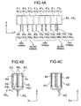
- Second terminals 49 1 and 49 2 are similarly provided on an end surface of the conductive member 42 n (42 1 and 42 2 ).
- the second terminals 49 n (49 1 and 49 2 ) have their roots folded so that their tips coincide with the arrangement of the first terminals 43 s , ... of one detector aggregate 40 mn .
- first terminals 43 1 , ... and the second terminal 49 1 or 49 2 are present between the first terminals 43 1 , ... and the second terminal 49 1 or 49 2 in order to collect charges. Accordingly, the roots of the conductive members 42 1 and 42 2 are folded so as to create a gap between the conductive member and the semiconductor base material 44 of the detector aggregate 40 mn to maintain electric insulation. As shown in Fig. 4B, all the first terminals 43 s and second terminals 49 n appear to be superimposed on one another as viewed from the side of the detector aggregate 40 mn .
- the second terminal 49 1 and the first terminals 43 2 and 43 3 have different poles. Accordingly, the second terminal 49 1 is separated from the first terminals 43 2 and 43 3 (43 6 and 43 7 ), arranged adjacent to the second terminal 49 1 , as shown in Fig. 4A, in order to prevent sparks, increase insulation lifetime, and reduce a leakage current. This is to apply high voltages to these electrodes so that positive and negative charges generated by the semiconductor base material 44 upon detecting a radiation can migrate efficiently to the corresponding electrodes (anode 46 A and cathode 47c).
- the first terminals 43 1 and 43 8 which are located at the opposite ends of the detector aggregate 40 mn , are arranged so as to reduce the spacing between themselves so that a terminal insertion hole 34 mn has a reduced opening area.
- Fig. 4C is a side view showing another embodiment of the detector aggregate 40 mn .
- a terminal 43 s ' is provided closer to the conductive member 42' 1 or 42' 2 .
- This arrangement enables a detector holding member 38 shown in Figs. 8A-8D, particularly the rotation operating member 36, to be located immediately below the detector aggregate 40 mn . This clarifies the positional relationship between the exposed part of the head 36a of the rotation operating member 36, shown in Figs. 8A-8D, and the corresponding detector aggregate 40mn.
- output terminals 33c jk are provided on a surface of the daughter board 32 1 which is opposite the one on which the detector aggregate 40 mn is placed; the output terminals 33c jk transmit a detected ⁇ ray detection signal.
- the output terminals 33c jk are provided on a back surface of the daughter board 32 h in association with each connecting device 33 jk .
- Input terminals 31c jk are provided on a front surface of the mother board 31; the input terminals 31c jk are connected to the output terminals 33c jk , and ⁇ ray detection signals are input through the input terminals 31c jk .
- the measuring circuit unit 8 (also see Fig. 1), provided on the back surface of the mother board 31 (which is opposite that surface on which the input terminals 31c jk are provided), has a function for converting the input ⁇ ray detection signals into a digital signal and outputting the processed signals to the data collecting and analyzing device 23 (see Fig. 1) .
- the measuring circuit unit 8 is a custom ASIC (Application Specific Integrated Circuit) designed and manufactured on the basis of system specifications.
- the measuring circuit unit 8 is further divided into a measuring processing circuit and a control processing circuit.
- the measuring processing circuit first amplifies each of the input ⁇ ray detection signal and measures a pulse height value.
- the control processing circuit forms a digital signal by adding, to the pulse height value, a value (trigger information) measured when the ⁇ ray detection signal is input and address information on the detector 1 (see Fig. 3) having provided the ⁇ ray detection signal.
- the digital signal is then input to the data collecting and analyzing device 23.
- the address information on the detector 1 is obtained by identifying an X axis wire 96 s and a Y axis signal read line 97 n , (see Figs. 7A and 7B) through which the ⁇ ray detection signal has been transmitted.
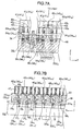
- the connecting device 33 jk will be described with reference to Figs. 7A and 7B and 8A to 8D.
- the connecting device 33 jk has a plurality of zero insertion force connectors 52. As many zero insertion force connectors 52 as the detector aggregates 40 mn are arranged in parallel in a housing 48 of the connecting device 33 jk ; the detector aggregates 40 mn are mounted on the connecting device 33 jk in the direction of the X axis.
- Each of the zero force insertion connectors 52 has a pressure contact member 37 s and a contact member 39 s , a pressure contact member 27 n and a contact member 29 n , and one rotation operating member 36.
- the paired pressure contact member 37 s and contact member 39 s and the paired pressure contact member 27 n and contact member 29 n are installed in a bottom portion of the housing 48 (see Figs. 7B and 8B).
- the paired pressure contact member 37 s and contact member 39 s lie opposite each other and the paired pressure contact member 27 n and contact member 29 n lie opposite each other.
- the first terminals 43 s are provided in the two detector aggregates 40 mn arranged in series in the direction of the Y axis.
- the second terminals 49 n are provided in the two detector aggregates 40 mn arranged in series in the direction of the Y axis.
- the paired contact members are arranged in a line along the longitudinal direction of the rotation operating member 36. The rotation operating member 36 is placed so as to extend in the direction of the Y axis.
- the opposite ends of the rotation operating member 36 are held by respective side walls (operation member support sections) of the housing 48.
- the operation member support sections support a detector support member 50 described later.
- One rotation operating member 36 is provided for the two detector aggregates 40 mn arranged in series and is placed beside the pressure contact member 37 s .
- the pressure contact members 37 s and 27 n are composed of leaf springs.
- the housing 48 has a plurality of terminal insertion holes 34 mn formed inside and having openings in their front surfaces.
- the housing 48 has the detector support member 50 at its upper end in which the opening is formed and which supports a bottom surface of each detector aggregate 40 mn .
- the first terminal 43 s and second terminal 49 n (see Figs. 3 and 4A) of each detector aggregate 40 mn are inserted into the opening in the detector support member 50.
- Each detector aggregate 40 mn is held by the detector support member 50 in the connecting device 33 jk .
- Two notches 35 formed in the opening of the terminal insertion hole 34 mn avoid contacting the roots of the above-described second terminals 49 1 and 49 2 (see Figs. 4A to 4C) with the detector support member 50.
- the notches 35 also position the held detector aggregate 40 mn .
- the detector aggregate 40 mn may have its surface provided with a thin insulating coating in order to prevent contact with another detector aggregate 40 mn .
- the conductive pressure contact member 37 s is placed in the terminal insertion hole 34 mn to elastically press the first terminal 43 s to hold the detector aggregate 40 mn , and to lead the ⁇ ray detection signal generated by the detection of ⁇ ray 10 to the daughter board 32 h .
- the conductive pressure contact member 27 n is also placed in the terminal insertion hole 34 mn to elastically press the second terminal 42 n to hold the detector aggregate 40 mn and to lead the ⁇ ray detection signal to the daughter board 32 h .
- the contact members 29 n and 39 s and rotation operating member 36 are also arranged in the terminal insertion hole 34 mn .
- Pads 37a s and 37c n are provided on the connecting device 33 jk ; the pad 37a, is formed at the terminal of the pressure contact member 37 s and pad 37c n is formed at the terminal of the pressure contact member 27 n .
- Pads 32a s and 32b n are provided on the daughter board 32 h .
- the pad 37a s is connected, in a BGA (Ball Grid Array) manner, to a pad 32a s connected to a wire 96 s located inside the daughter board 32 h .
- the ⁇ ray detection signal led to the wire 96 s via the pressure contact member 37 s is output to the mother board 31 through the output terminal 33c jk .
- the BGA connection is a solder connection based on a reflow process.
- the pad 37c n is connected, in the BGA manner, to a pad 32b n connected to a wire 97 n inside the daughter board 32 h .
- the ⁇ ray detection signal led to a wire 97 n via the pressure contact member 27 n is output to the mother board 31 through the output terminal 33c jk .
- the pad 37a s may be formed at the terminal of the contact member 39 s rather than at the terminal of the pressure contact member 37 s by extending the contact member 39 s to the bottom surface of the housing 48.
- the pad 37c n may be formed at the terminal of the contact member 29 n rather than at the terminal of the pressure contact member 27 n by extending the contact member 29 n to the bottom surface of the housing 48.
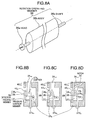
- the rotation operating member 36 has a head 36a in which the tip of a removal tool 47 (see Fig. 6) such as a driver is fitted, a body portion 36b with an elliptical cross section, and a shaft 36c rotatably supported by the connecting device 33 jk (see Fig. 4).
- a removal tool 47 such as a driver
- One rotation operating member 36 is provided for each terminal insertion hole 34 mn (see Fig. 6).
- the rotation operating member 36 is rotatably supported by the housing 48 so that its longitudinal direction coincides with the longitudinal direction of the detector aggregate 40 mn .
- the rotation operating member 36 together with the pressure contact member 37 s , elastically presses a side surface of the first terminal 43 s inserted into the terminal insertion hole 34 mn toward the contact member 39 s .
- the rotation operating member 36, the pressure contact member 37 s , and the contact member 39 s form the detector holding member 38 (see Fig. 8B) holding the detector aggregate 40 mn across the first terminal 43 s .
- the rotation operating member 36, together with the pressure contact member 27 n elastically presses a side surface of the second terminal 49 n inserted into the terminal insertion hole 34 mn toward the contact member 29 n .
- the rotation operating member 36, the pressure contact member 27 n , and the contact member 29 n form the detector holding member 28 (see Fig. 8D) holding the detector aggregate 40 mn across the second terminal 49 n .
- the pressure contact member 37s constitutes an elastically flexibly deformed cantilever.
- the pressure contact member 37 s has a projection-like contact 37b s at its free end so that it can mechanically and electrically contact the first terminal 43 s .
- a projection-like contact 27b n is also provided at the tip of the pressure contact member 27 n .
- the removal tool 47 is used to rotatively move the rotation operating member 36 so that the longitudinal direction of cross section of the rotation operating member 36 coincides with the direction of the Z axis (see Fig. 8B). With the longitudinal direction of cross section of the rotation operating member 36 coinciding with the direction of the Z axis, the pressure contact member 37 s of the detector holding member 38 does not contact the body portion 36b of the rotation operating member 36.
- the width of a gap formed between the pressure contact member 37 s and the contact member 39 s is equal to or larger than the thickness of the first terminal 43 s (the same as the thickness of the second terminal 49 n ).
- the width of a gap formed between the pressure contact member 27 n and the contact member 29 n is also equal to or larger than the thickness of the first terminal 43 s .
- Each second terminal 49 n is inserted between the corresponding pressure contact member 27 n and contact member 29 n .
- each terminal can be inserted between the pressure contact member and the contact member without sliding the side surface of the terminal on the pressure contact member or contact member.
- each terminal is inserted between the pressure contact member and the contact member without any insertion force.
- the head 36a (see Fig. 8A) of the rotation operating member 36 is rotated using the removal tool 47 through 90°.
- the longitudinal direction of cross section of the rotation operating member 3 is then orthogonal to the first terminals (or second terminals).
- the state in which the longitudinal direction of cross section of the rotation operating member 3 is orthogonal to the first terminals (or second terminals) includes the state in which the longitudinal direction is orthogonal to extensions of the first terminals (or second terminals).
- an outer surface of the body portion 36b contacts a side surface of the pressure contact member 37 s to press the pressure contact member 37 s toward the contact member 39 s .
- the pressure contact member 37 s is flexibly deformed (see Fig. 8C).
- the contact 37b s contacts a side surface of the first terminal 43 s positioned between the pressure contact member 37 s and the contact member 39 s . This makes the first terminal 43 s and the pad 37a s electrically conductive to enable an analog signal provided by the detector aggregate 40 mn to be output through the pad 37a s .
- the contact 27b n contacts the second terminal 49 n positioned between the pressure contact member 27 n and the contact member 29 n to make the second terminal 49 n and the pad 37c n electrically conductive.
- each detector 1 is attached to the zero insertion force connector 56 to mount the detector aggregates 40 81 and 40 82 on the connecting device 33 jk . That is, the detector aggregates 40 81 and 40 82 are mounted on the daughter board 32 h . The other detector aggregates 40 mn are similarly mounted on the connecting device 33 jk . Owing to their high rigidity, the contact members 29 n and 39 s are not deformed even under the pressure of the pressure contact member.
- the anode 46 A , conductive member 41 s , cathode 47 c , and conductive member 42 n of the detector aggregate 40 mn are arranged perpendicularly to the daughter board 32 h .
- the plurality of detectors 1 are arranged in a certain direction (for example, the X axis direction).
- a plurality of the detectors 1 are arranged in a different direction (for example, the Y axis direction) orthogonal to the above direction.
- the rotation operating member 36 is further rotated through 90° using the removal tool 47. Then, as shown in Fig. 8B, the pressure member 37 s leaves the pressure contact member 37 s to cancel the pressure of the contact 37b s on the first terminal 43 s . The pressure on the second terminal 49 n is also cancelled.
- the detector 1, that is, the detector aggregate 40 mn , (40 81 , 40 82 ) can be removed from the connecting device 33 jk , that is, the zero insertion force connector 52 without exerting a frictional force.
- the present embodiment no thermal process (solder reflow or the like) is required in mounting the detector 1 on the daughter board 32 h .
- This enables the use of detectors 1 having characteristics impaired by heating history.
- the present embodiment is also significantly advantageous in that if detectors 1 are used which are not substantially affected by a single thermal process, a thermal process required to replace some defective detectors 1 does not fatigue surrounding detectors 1 even with heat cycles.
- the first terminal 43 s of the detector aggregate 40 mn is inserted between the pressure contact member 37 s and the contact member 39 s , which are open.
- the second terminal 42 n of the detector aggregate 40 mn is inserted between the pressure contact member 27 n and the contact member 29 n , which are open. Then, the detector aggregate 40 mn can be held on the detector support member 50. Accordingly, rotation of the rotation operating member 36 enables the detector aggregate 40 mn to be easily attached to the zero insertion force connector 52.
- the gap between the pressure contact member 37 s and the contact member 39 s which are open, is located immediately below the corresponding opening formed in the detector support member 50.
- the gap between the pressure contact member 27 n and the contact member 29 n , which are open, is located immediately below the corresponding opening formed in the detector support member 50. Without the detector support member 50, the detector aggregate 40 mn must be gripped using a certain method until the detector aggregate 40 mn is attached to the zero insertion force connector 52 by rotating the rotation operating member 36.
- the detector holding member 38 allows the pressure contact member 37 s and the rotation operating member 36 to cooperate in holding the detector aggregate 40 mn .
- the connecting device 33 jk is not limited to such a configuration. Any structure can be used provided that it enables the detector 1 to be installed and removed without any insertion force (with zero frictional force) .
- the detector 1a has the anode 3 and the cathode 4 on two surfaces of the semiconductor base material 44A so that the semiconductor base material 44A is sandwiched between the anode 3 and the cathode 4.
- the anode 3 and the cathode 4 are conductive metal plates.
- each of the anodes 3 is connected to a wire 12 extending in the X axis direction.
- each of the cathodes 4 is connected to a wire 14 extending in the Y axis direction.
- the plurality of detectors 1 connected together in one direction have their anodes 3 electrically connected together using one wire 12. Further, the plurality of detectors 1 connected together in a direction orthogonal to the above direction have their cathodes 4 electrically connected together using one wire 14.
- This wiring structure is called a matrix structure.
- a ⁇ ray is incident on one of the detectors 1, specifically the semiconductor base material 44, to generate charges through interaction. Then, information ( ⁇ ray detection signal) on the charges is obtained through the wires 12 and 14 connected to the detector 1. Simultaneity determination enables the identification of the wires 12 and 14 having simultaneously obtained the information on the charges. This makes it possible to determine that the ⁇ ray has entered the detector 1 connected to the identified wires 12 and 14.
- wires 96 s and 97 n are provided in the daughter board 32 h for each connector device 33 jk ; the wire 96 s extends in the X axis direction, the wire 97 n extends in the Y axis direction, the wires 96 s and 97 n constitute the wire matrix structure shown in Fig. 9.
- the common wire 96 s electrically connects to the first terminals 43 s (for example, the first terminals 43 1 ) of the detector aggregates 40 ml adjacent to each other in the X axis direction as shown in Figs. 7A and 7B.
- Separate wires 96 s connect to the first terminals 43 2 , 43 3 , and the like of the detector aggregates 40 m1 adjacent to each other in the X axis direction.
- the common wire 97 1 connects the second terminals 49 1 of the two detector aggregates 40 51 and 40 52 , which are arranged in the Y axis direction.
- the common wire 97 2 connects the second terminals 49 2 of the detector aggregates 40 51 and 40 52 .
- the common wire 97 n connects the second terminals 49 n of the two other detector aggregates 40 mn arranged in the Y axis direction.
- the wires 96s and 97n are connected to the measuring circuit unit 8 via the mother board 31.
- the measuring circuit unit 8 has a signal processing device (not shown) for each connecting device 33 jk .
- the signal processing device carries out a simultaneity determination on for one connecting device 33 jk on the basis of charge information input to the wires 96 s and 97 n .
- the measuring circuit unit 8 thus identify the wires 96 s and 97 n having simultaneously obtained the charge information.
- the detector 1 connected to the identified wires 96 s and 97 n has detected the ⁇ ray 10.
- the signal processing device thus recognizes the position of the detector 1 having detected the ⁇ ray 10.
- the data collecting and analyzing device 23 creates tomography information on the patient P on the bases of the positional data on the detector 1 having detected the ⁇ ray, the data having output by the corresponding signal processing device in the measuring circuit unit 8.
- the present embodiment has the above wire matrix structure. Consequently, if for example, n x n detectors 1 are provided, the number of signal read channels connected to the detector 1 is sharply reduced to 2n. This makes it possible to reduce the size of detector pixels and to arrange the signal read channels behind the detector aggregate 40 mn . Further, the reduction in the number of signal read channels contributes to miniaturization of the semiconductor radiation detecting device 30.
- a capacitive element (not shown) and a resistive element (not shown) using for wiring of the matrix structure are installed on the back surface of the daughter board (first support substrate) 32 h and between the output terminals 33 Cjk (or on the front surface of the mother board and between the input terminals 31c jk ); the capacitive element is positioned between the detector 1 and the measuring circuit unit 8 and connected to them, and the resistive element is positioned between the detector 1 and the high voltage power source and connected to them.
- the terminals (first terminal 43 s and second terminal 49 n ) connected to each electrode of the detector 1 can be detachably attached to the zero insertion force connector 52.
- the zero insertion force connector 52 enables the detector aggregate 40 mn , that is, the detector 1, to be easily replaced with a new one.
- the detector 1, that is, the detector aggregate 40 mn that becomes defective in use is desirably replaced with a new one.
- a new detector aggregate 40 mn can also be easily attached to the connector 52.
- the replacement of the detector aggregate 40 mn may be carried out with the daughter board 32 h removed from the mother board 31.
- Fig. 8B when each terminal of the detector aggregate 40 mn is inserted between the pressure contact member and contact member of the zero insertion force connector 52 using the vacuum tweezers, no frictional force is exerted between the terminal and the pressure contact member and contact member. That is, in inserting the detector 1 into the zero insertion force connector 52, it is unnecessary to exert a force for pushing the detector 1 in the connector. Further, no frictional force is exerted when each terminal of the detector aggregate 40 mn is pulled out of the zero insertion force connector 52. Thus, when each terminal is inserted into and pulled out of the zero insertion force connector 52, the detector aggregate 40 mn does not incline.
- the detector aggregate 40 mn prevents the detector aggregate 40 mn from contacting the end surface (that is not covered with the conductive member 42 n ) of the semiconductor base material 44 of the adjacent detector aggregate 40 mn . It is thus possible to prevent damage to the semiconductor base material 44 of the adjacent detector aggregate 40 mn , which has a low mechanical intensity. As described above, the detector aggregate 40 mn does not incline when the terminal is inserted or pulled out. Accordingly, the clearance between the adjacent detector aggregates 40 mn can be reduced taking electric insulation into account.
- the detector aggregates 40 mn that is, the detectors 1, can be more densely arranged while preventing damage to the semiconductor base materials 44. This makes it possible to further improve the sensitivity and spatial resolution of the detector 1.
- the improvement of the detector sensitivity leads to a further reduction in the time required for checks.
- the application of the zero insertion force connector enables the detectors 1 to be densely arranged while allowing each detector aggregate 40 mn to be replaced with a new one.
- the detector 1 can be connected to the daughter board 32 h without any thermal process such as soldering. Consequently, the detectors 1, which are not resistant to high temperature, can be densely mounted.
- the first terminal 43 s and second terminal 49 n included in the two sub-aggregates 45A and 45B are attached to the zero insertion force connector 52. This reduces the number of zero insertion force connectors 52 required, thus simplifying the structure of the semiconductor radiation detecting device 30.
- the first terminal 43 s and second terminal 49 n of each of the plurality of detector aggregates 40 mn are attached to one zero insertion force connector 52; the detector aggregates 40 mn are arranged in series in a certain direction (the longitudinal direction of the rotation operating member 36 or the longitudinal direction of the semiconductor base material 44). This further reduces the number of zero insertion force connectors 52 required, thus further simplifying the structure of the semiconductor radiation detecting device 30.
- the detector aggregate 40 mn when the rotation operating member 36 is rotated, that is, operated, the detector aggregate 40 mn can be held on the detector support member 50. This allows the detector aggregate 40 mn to be easily attached to the zero insertion force connector 52.
- the head 36a which is used for rotate the rotation operating member 36, is exposed from one end surface of the daughter board 32 h , that is, one surface of the housing 48.
- the head 36a can be easily accessed by the removal tool 47.
- the anode 46 A and cathode 47 c of the detector 1 are arranged perpendicularly to the daughter board 32 h . Accordingly, compared to a horizontal arrangement with respect to the daughter board 32 h , the perpendicular arrangement enables the detectors 1 to be densely located. This is because the perpendicular arrangement enables a reduction in the size of the gap between the adjacent detector aggregates 40 mn which gap is required to arrange conductive members such as wires for connecting electrode films to wires provided in the support substrate.
- the conductive member 41 s is used to connect the cathodes 47 s of the two detectors 1 together, while the conductive member 41 s is used to connect together the anodes 46 s of the eight detectors 1 arranged in a row.
- the wire matrix structure is thus employed in the initial stage of wiring. This enables easy connecting operations. It is thus possible to quickly complete the wiring of the matrix structure in the daughter board 32 h , which is connected to the pads 37Aa s and 37c n of the zero insertion force connector 52.
- the first terminal 43 s and second terminal 49 n (see Fig. 3) of each of the detector aggregates 40 m1 and 40 m2 are attached to one set of the pressure contact member and contact member positioned close to one operating member 36; the detector aggregates 40 m1 and 40 m2 are arranged in series in the Y axis direction.
- the first terminal 43 s of each of the detector aggregates 40 m1 and 40 m2 may be attached to a first set of the pressure contact member and contact member positioned close to one operating member 36.
- the second terminal 49 n of each of the detector aggregates 40 m1 and 40 m2 may be attached to a second set of the pressure contact member and contact member positioned close to another operating member 36.
- the first and second sets are arranged in parallel.
- the pressure contact member and contact member of each set are installed in the bottom portion of the housing 48.
- the detectors 1A, 1B, 1C, 1D, 1E, 1F, 1G, and 1H share the one elongate semiconductor base material 44.
- each of the detectors may comprise one semiconductor base material.
- the detectors 1A, 1B, 1C, 1D, 1E, 1F, 1G, and 1H are separated from one another.
- the detectors 1 are integrated by the conductive member 42.
- the detectors 1A, 1B, 1C, 1D, 1E, 1F, 1G, and 1H share one elongate semiconductor base material 33.
- each of the detectors 1A, 1B, 1C, 1D, 1E, 1F, 1G, and 1H may comprise one semiconductor base material.
- the detectors 1A, 1B, 1C, 1D, 1E, 1F, 1G, and 1H are separated from one another but are integrated together by the conductive member 42, attached to the cathode 47 c .
- the anodes 46 A of the two sub-aggregates are connected together by the conductive member 41 s .
- the above technical concept is applicable to the plurality of detectors 1a arranged in the X axis direction as shown in Fig. 9. This arrangement should also be included in the scope of the present invention.
- the anode 3 shown in Fig. 9 is provided with a first terminal (not shown).
- the cathode 4 is provided with a second terminal (not shown).
- the above paired pressure contact member 37 s and contact member 39 s and paired pressure contact member 27 n and contact member 29 n are arranged in the X axis direction.
- the first and second terminals of a plurality of detectors 1a arranged in the X axis direction are inserted between the pressure contact member and the contact member. Then, the rotation operating member 36 is rotated. This enables the first and second terminals of each detector 1a to be attached to zero insertion force connector 52 without any insertion force.
- the detector 1a can be mounted on the support substrate.
- a plurality of the detectors 1a arranged in the X axis direction may have their cathodes 4 integrated, with one second terminal attached to the integrated cathodes.
- a plurality of the first terminals and one second terminal of the plurality of detectors 1a are attached to the one zero insertion force connector 52.
- the detectors are applied to the SPECT apparatus (Single Photon Emission CT apparatus) by way of example.
- the present invention is not limited to this.
- the detectors may be applied to a PET (Positron Emission Tomography apparatus).
Landscapes
- Physics & Mathematics (AREA)
- Health & Medical Sciences (AREA)
- Life Sciences & Earth Sciences (AREA)
- General Physics & Mathematics (AREA)
- High Energy & Nuclear Physics (AREA)
- Molecular Biology (AREA)
- Spectroscopy & Molecular Physics (AREA)
- Measurement Of Radiation (AREA)
- Nuclear Medicine (AREA)
- Light Receiving Elements (AREA)
Abstract
A radiological imaging apparatus allowing semiconductor radiation detectors to be easily replaced with new ones and densely arranged. Terminals (31cjk) and (33cjk) are provided on a bottom surface of a detector aggregate (40mn) including a plurality of semiconductor radiation detectors (1); the terminals is connected to electrodes (3 and 4) of the detectors (1). A plurality of zero insertion force connectors (56) are provided on a connecting device (33jk) installed on a support substrate (32h). The terminals (31cjk and 33cjk) are detachably attached to the zero insertion force connectors (56) to mount the detector aggregates (40mn) that are the semiconductor radiation detectors (1), on the support substrate (32h). When the detector aggregates (40mn) are attached to the zero insertion force connectors (56), since no frictional force acts on the terminals, the size of the gap between the detector aggregates (40mn) is reduced.
Description
- The present invention relates to a radiological imaging apparatus, and in particular, to a radiological imaging apparatus using a semiconductor radiation detector.
- In the prior art, a semiconductor radiation detector is electrically connected to wiring placed inside a support substrate using a method such as soldering, while being mechanically held on the support substrate (Third Edition of Radiation Measurement Handbook (NIKKAN KOGYO SHIMBUN LTD.), p.559).
- Conventionally, an operation of replacing a semiconductor radiation detector is not easy because of the need for a soldering process. On the other hand, the semiconductor radiation detector may use a connector that requires an insertion force to push a male terminal provided on the detector, in a spring of a female terminal. The female terminal is provided in the connector. Even a low insertion connector (LIF) requires a force of about several grams/pin to push the semiconductor radiation detector. The inventors have found that when the semiconductor radiation detector is pushed in the connector requiring an insertion force, a load on the semiconductor radiation detector exerts a strong frictional force between the male terminal on the semiconductor radiation detector and the spring of the female terminal, making the semiconductor radiation detector likely to incline. The inventors have also found that the inclining semiconductor radiation detector may slidably contact and damage a delicate semiconductor member of an adjacent semiconductor radiation detector. This problem may also occur when the semiconductor radiation detector is pulled out of its connector for replacement; also in this case, the adjacent semiconductor radiation detector may be damaged. This problem can be avoided by increasing the clearance between the semiconductor radiation detectors installed on the support substrate to the extent that the semiconductor member is not damaged by the contact. However, the formation of such a clearance causes the semiconductor radiation detectors to be more densely arranged. This prevents the further improvement of sensitivity and spatial resolution of the semiconductor radiation detector.
- It is an object of the present invention to provide a radiological imaging apparatus that enables semiconductor radiation detectors to be more densely arranged.
- To accomplish this object, the present invention is characterized that a plurality of semiconductor radiation detectors are detachably attached to a plurality of non-insertion connectors provided on a support substrate, a first electrode of each of the semiconductor radiation detectors is connected to a first wire provided in the support substrate via the corresponding zero insertion force connector, and a second electrode of the semiconductor radiation detector is connected to a second wire provided in the support substrate via the zero insertion force connector.
- The semiconductor radiation detector is thus detachably attached to the zero insertion force connector. This substantially eliminates the need for a force for pushing the semiconductor radiation detector in the zero insertion force connector when the semiconductor radiation detector is inserted into the connector. This in turn reduces the degree of damage done to the semiconductor radiation detector by the semiconductor member of the adjacent one when the latter is inserted into the zero insertion force connector, even with a reduced clearance between the semiconductor radiation detectors. Therefore, it is possible to reduce the clearance between the semiconductor radiation detectors and to enable the semiconductor radiation detectors to be more densely arranged using the support substrate. The more dense arrangement of the semiconductor radiation detectors makes it possible to further improve the sensitivity and spatial resolution of each semiconductor radiation detector. The improvement of the detector sensitivity further reduces the time required for checks. Further, the application of the zero insertion force connectors allows the semiconductor radiation detector to be easily replaced with a new one.
- Preferably, the first and second wires arranged in the support substrate have a matrix structure. This reduces the number of wires and the size of an area required to install the wires. This in turn increases the size of a free space in the support substrate in which the wires can be installed, thus contributing to increasing the density of arrangement of semiconductor radiation detectors. Further, the matrix structure of the wires enables a sharp reduction in the number of measuring circuits. This contributes to reducing the size of a detector head.
- The present invention enables semiconductor radiation detectors to be more densely arranged while allowing each of the semiconductor radiation detectors to be replaced with a new one.
- Other objects, features and advantages of the invention will become apparent from the following description of the embodiments of the invention taken in conjunction with the accompanying drawings.
-
- Fig. 1 is a diagram showing the whole SPECT apparatus in accordance with a first embodiment of the present invention;
- Fig. 2A is a detailed perspective view of a radiation detecting unit shown in Fig. 1, and Fig. 2B is a partly enlarged perspective view showing that part of the radiation detecting unit shown in Fig. 2A which is shown by arrow A;
- Fig. 3 is an exploded perspective view of a detector aggregate shown in Fig. 2B;
- Fig. 4A is a front view of the detector aggregate, Fig. 4B is a side view of the detector aggregate, and Fig. 4C is a side view of another embodiment of the detector aggregate;
- Fig. 5A is a front view of the radiation detecting unit shown in Fig. 2B as viewed from the direction of an X axis in the figure, and Fig. 5B is a side view of the radiation detecting unit as viewed from the direction of a Y axis;
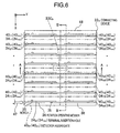
- Fig. 6 is a top view of a connecting device shown in Figs. 2A and 2B;
- Fig. 7A is a sectional view partly showing a cross section of the connecting device shown in Fig. 6, the cross section being taken along line A-A, and Fig. 7B is a sectional view of the connecting device taken along line B-B in Fig. 6;
- Figs. 8A-8D are an enlarged sectional view of the internal configuration of the connecting device shown in Figs. 2A and 2B, wherein Fig. 8A is an enlarged perspective view of a rotative movement member, Fig. 8B is an enlarged sectional view of that part of the connecting device shown in Fig. 7B which is shown by arrow D, the figure showing that holding of a detector is cancelled, Fig. 8C is an enlarged sectional view of a part of Fig. 7B shown by arrow E, the figure showing that the detector is held, and Fig. 8D is a view of a cross section passing through a notch; and
- Fig. 9 is a conceptual drawing illustrating a wire matrix structure.
- Embodiments of the present invention will be described below with reference to Figs. 1 and 8A to 8D.
- With reference to Fig. 1, description will be given of a single photon emission computer tomography apparatus (referred to as a SPECT apparatus below) that is an example of a semiconductor radiological imaging apparatus in accordance with an embodiment of the present invention. The
SPECT apparatus 51 comprises a bed B that supports a patient P that is a subject, a pair of semiconductor radiation detecting devices (detector heads) 30, arotating support 56, a data collecting and analyzingdevice 23, adata input device 24, and adisplay device 25. The semiconductorradiation detecting devices 30 are installed on therotating support 56 so as to be offset from each other by 180° in a circumferential direction. The semiconductorradiation detecting devices 30 project from the rotatingsupport 56 in a longitudinal direction of the bed B. The bed B is inserted between the two opposite semiconductorradiation detecting device 30. Each of the semiconductorradiation detecting devices 30 comprises asupport member 6, a measuringcircuit unit 8, aradiation detector unit 11, and acollimator 54 which are installed on therotating support 56. Thesupport member 6 is mounted on therotating support 56 so as to be movable in a radial direction of therotating support 56. The measuringcircuit unit 8,radiation detector unit 11, andcollimator 54 are mounted on thesupport member 6. Eachradiation detector unit 11 faces toward the bed B. Thecollimator 54 is placed between theradiation detector unit 11 and the bed B to limit the view angles from semiconductor radiation detectors (referred to as detectors below) 1 of theradiation detecting unit 11. Theradiation detecting unit 11,collimator 54, and measuringcircuit unit 8 are housed in a light blockingelectromagnetic shield 7 attached to thesupport member 6. The light blockingelectromagnetic shield 7 blocks radiations emitted by an affected part C, that is, electromagnetic waves different from aγ ray 10. The light blockingelectromagnetic shield 7 thus prevents the electromagnetic waves from affecting theradiation detecting unit 11 and the measuringcircuit unit 8. Instead of the pair, three semiconductorradiation detecting devices 30 may be provided. - The bed B is moved on which the patient P to which a radioactive agent has been administered lies. The patient P is thus moved to between the pair of semiconductor
radiation detecting devices 30. Theγ ray 10 is emitted from the affected part C in the patient P in which the radioactive agent has been collected. Theray 10 is then incident on each of thedetector 1 of theradiation detecting unit 11 through a through-hole portion in thecollimator 54. Thedetector 1 outputs a γ ray detection signal (analog signal) to the measuringcircuit unit 8, which then processes the signal. The data collecting and analyzingdevice 23 uses information output by the measuringcircuit unit 8 to create a tomography information on the patient P. The data collecting and analyzingdevice 23 then displays the tomography information on thedisplay device 25. The rotatingsupport 56 is rotated to pivot the semiconductorradiation detecting device 30, including theradiation detecting unit 11, around the patient P. With the semiconductorradiation detecting device 30 pivoting, eachdetector 1 detects theγ ray 10 to output the γ ray detection signal. The following operations can be performed near theSPECT apparatus 51 using an operation panel 58: control of rotation of therotating support 56, control of the distance between theradiation detecting unit 11 and the patient P, and control of position of the patient P using the bed. These operations can also be remotely performed using adata input device 24. - Now, with reference to Figs. 2A and 2B, description will be given of the
radiation detecting unit 11 used in the present embodiment. - The
radiation detecting unit 11 comprises onemother board 31 that is a second support substrate, a plurality of (in the figure, five) daughter boards 32h (321, 322, ...) placed on the surface of the second support substrate that are first support substrates, and a plurality of detector aggregates 40mn that are detachably attached on each of the daughter boards 32h (see Figs. 2B and 3). The width of thedaughter board 32h is determined by the number of connecting devices 33jk that can be opened and closed by one rotation operating member (operation member) 36 as described later. If the semiconductorradiation detecting device 30 can be entirely operated from end to end using the singlerotation operating member 36, the connecting device 33jk can be mounted directly on themother board 31 without using thedaughter board 32h. - The
daughter board 32h has the detector aggregate 40mn (see Figs. 2B and 3) provided on its surface to detect theγ ray 10; a longitudinal direction of thedetector aggregate 40mn is aligned with the direction (across the Y axis in the figure) in which theradiation detecting unit 11 is rotatively moved. The longitudinal direction of thedetector aggregate 40mn is aligned with the rotatively moving direction of theradiation detecting unit 11 because this makes it possible to avoid the effect (vibration or the like) of an inertia force on thedetector aggregate 40mn which is exerted as the rotation of theradiation detecting unit 11 is accelerated or decelerated, thus preventing electrodes from being bent. Thedaughter board 32h puts together faint analog signals provided by thedetector aggregate 40mn upon detecting theγ ray 10. Thedaughter board 32h then outputs the resulting signal to themother board 31. Thedetector aggregate 40mn is detachably mounted on the connecting device 33jk, provided on a surface of thedaughter board 32h, as described later. As described later in detail, thedetector aggregate 40mn is attached and removed by rotatively moving ahead 36a of therotation operating member 36, exposed at an end of thedaughter board 32h. - Thus, in Figs. 2A and 2B, five
daughter boards 32h (h=1 to 5) are provided on onemother board 31, and 2x10, that is, 20 connecting devices 33jk (j=1 to 10, k=1 or 2) are provided on thedaughter board 32h, and 16 (8x2) detector aggregates 40mn(m=1 to 8, n=1 or 2) are provided on the connecting device 33jk. Onedetector aggregate 40mn has 16detectors 1 as shown in Fig. 3, described below. One detector constitutes one pixel range. The numbers of components arranged shown above are only illustrative and may be increased or reduced depending on the purpose. - The
detector aggregate 40mn will be specifically described with reference to Figs. 3 and 4A to 4C. - The
detector aggregate 40mn has twosub-aggregates cathodes 47c (c=1 to 8) separately provided on the other surface of thesemiconductor base material 44 at predetermined intervals. The anodes 46A and thecathodes 47c are formed by depositing a conductive metal on the surface of thesemiconductor base material 44. Thesemiconductor base material 44 is composed of cadmium telluride (CdTe) or the like, which generates charges when theγ ray 10 is incident on thesemiconductor base material 44. Thesemiconductor base material 44 has a planar shape, and its longitudinal direction corresponds to the direction of the Y axis in the figure. Each of the anodes 46A lies opposite the correspondingcathode 47c across thesemiconductor base material 44. Onedetector 1 is composed of one anode 46A, thecathode 47c lying opposite this anode 46A, and a part of thesemiconductor base material 44, located between the anode 46A and thecathode 47c. Each of the sub-aggregates 45A and 45B has substantially eightdetectors 1, specifically,detectors conductive member 41s is located between the anode 46A in the sub-aggregate 45A and the anode 46A in the sub-aggregate 45B. The two conductive members 42n (421 and 422) are attached separately to the eightcathodes 47c in the sub-aggregate 45B and to the eightcathodes 47c in the sub-aggregate 45B using a conductive adhesive. Theconductive members 41s and 42n are composed of plates of conductive metal (for example, copper). - The
detector aggregate 40mn is thus configured, so that one detector forms one pixel. That is, onedetector aggregate 40mn provides 16 pixels. - As shown in Figs. 3 and 4A, first terminals 43s (431, 432, 433, 434, 435, 436, 437, and 438) (s=1 to 8) project from the
semiconductor base material 44 and extend from an end surface of the respectiveconductive members 41s along a Z axis.Second terminals first terminals 43s, ... of onedetector aggregate 40mn. Further, a large potential difference of several hundred V is present between thefirst terminals 431, ... and thesecond terminal semiconductor base material 44 of thedetector aggregate 40mn to maintain electric insulation. As shown in Fig. 4B, all thefirst terminals 43s andsecond terminals 49n appear to be superimposed on one another as viewed from the side of thedetector aggregate 40mn. - The
second terminal 491 and thefirst terminals 432 and 433 (436 and 437) have different poles. Accordingly, thesecond terminal 491 is separated from thefirst terminals 432 and 433 (436 and 437), arranged adjacent to thesecond terminal 491, as shown in Fig. 4A, in order to prevent sparks, increase insulation lifetime, and reduce a leakage current. This is to apply high voltages to these electrodes so that positive and negative charges generated by thesemiconductor base material 44 upon detecting a radiation can migrate efficiently to the corresponding electrodes (anode 46A andcathode 47c). Thefirst terminals detector aggregate 40mn, are arranged so as to reduce the spacing between themselves so that aterminal insertion hole 34mn has a reduced opening area. - Fig. 4C is a side view showing another embodiment of the
detector aggregate 40mn. A terminal 43s' is provided closer to the conductive member 42'1 or 42'2. This arrangement enables adetector holding member 38 shown in Figs. 8A-8D, particularly therotation operating member 36, to be located immediately below thedetector aggregate 40mn. This clarifies the positional relationship between the exposed part of thehead 36a of therotation operating member 36, shown in Figs. 8A-8D, and the corresponding detector aggregate 40mn. - As shown in Figs. 5A and 5B, output terminals 33cjk are provided on a surface of the
daughter board 321 which is opposite the one on which thedetector aggregate 40mn is placed; the output terminals 33cjk transmit a detected γ ray detection signal. The output terminals 33cjk are provided on a back surface of thedaughter board 32h in association with each connecting device 33jk. - Input terminals 31cjk are provided on a front surface of the
mother board 31; the input terminals 31cjk are connected to the output terminals 33cjk, and γ ray detection signals are input through the input terminals 31cjk. The measuring circuit unit 8 (also see Fig. 1), provided on the back surface of the mother board 31 (which is opposite that surface on which the input terminals 31cjk are provided), has a function for converting the input γ ray detection signals into a digital signal and outputting the processed signals to the data collecting and analyzing device 23 (see Fig. 1) . - The measuring
circuit unit 8 is a custom ASIC (Application Specific Integrated Circuit) designed and manufactured on the basis of system specifications. The measuringcircuit unit 8 is further divided into a measuring processing circuit and a control processing circuit. The measuring processing circuit first amplifies each of the input γ ray detection signal and measures a pulse height value. Then, the control processing circuit forms a digital signal by adding, to the pulse height value, a value (trigger information) measured when the γ ray detection signal is input and address information on the detector 1 (see Fig. 3) having provided the γ ray detection signal. The digital signal is then input to the data collecting and analyzingdevice 23. The address information on thedetector 1 is obtained by identifying anX axis wire 96s and a Y axis signal readline 97n, (see Figs. 7A and 7B) through which the γ ray detection signal has been transmitted. - The connecting device 33jk will be described with reference to Figs. 7A and 7B and 8A to 8D. In Fig. 6, the contours of the (in the figures, 8x2=16) detector aggregates 40mn mounted on the connecting device 33jk are shown by alternate long and two short dashes lines so that the arrangement of the detector aggregates 40mn can be understood. The connecting device 33jk has a plurality of zero
insertion force connectors 52. As many zeroinsertion force connectors 52 as the detector aggregates 40mn are arranged in parallel in ahousing 48 of the connecting device 33jk; the detector aggregates 40mn are mounted on the connecting device 33jk in the direction of the X axis. Each of the zeroforce insertion connectors 52 has apressure contact member 37s and acontact member 39s, apressure contact member 27n and acontact member 29n, and onerotation operating member 36. There are 16pressure contact members 37s andcontact members pressure contact members contact members 39n. The pairedpressure contact member 37s andcontact member 39s and the pairedpressure contact member 27n andcontact member 29n are installed in a bottom portion of the housing 48 (see Figs. 7B and 8B). The pairedpressure contact member 37s andcontact member 39s lie opposite each other and the pairedpressure contact member 27n andcontact member 29n lie opposite each other. As many pairs of thepressure contact member 37s andcontact member 39s asfirst terminals 43s are provided; thefirst terminals 43s are provided in the two detector aggregates 40mn arranged in series in the direction of the Y axis. As many pairs of thepressure contact member 27n andcontact member 29n assecond terminals 49n are provided; thesecond terminals 49n are provided in the two detector aggregates 40mn arranged in series in the direction of the Y axis. The paired contact members are arranged in a line along the longitudinal direction of therotation operating member 36. Therotation operating member 36 is placed so as to extend in the direction of the Y axis. The opposite ends of therotation operating member 36 are held by respective side walls (operation member support sections) of thehousing 48. The operation member support sections support adetector support member 50 described later. Onerotation operating member 36 is provided for the two detector aggregates 40mn arranged in series and is placed beside thepressure contact member 37s. Thepressure contact members - The
housing 48 has a plurality of terminal insertion holes 34mn formed inside and having openings in their front surfaces. Thehousing 48 has thedetector support member 50 at its upper end in which the opening is formed and which supports a bottom surface of eachdetector aggregate 40mn. Thefirst terminal 43s and second terminal 49n (see Figs. 3 and 4A) of eachdetector aggregate 40mn are inserted into the opening in thedetector support member 50. Eachdetector aggregate 40mn is held by thedetector support member 50 in the connecting device 33jk. Twonotches 35 formed in the opening of theterminal insertion hole 34mn avoid contacting the roots of the above-describedsecond terminals 491 and 492 (see Figs. 4A to 4C) with thedetector support member 50. Thenotches 35 also position the helddetector aggregate 40mn. - The
detector aggregate 40mn may have its surface provided with a thin insulating coating in order to prevent contact with anotherdetector aggregate 40mn. - As shown in Figs. 7A and 7B, the conductive
pressure contact member 37s is placed in theterminal insertion hole 34mn to elastically press thefirst terminal 43s to hold thedetector aggregate 40mn, and to lead the γ ray detection signal generated by the detection ofγ ray 10 to thedaughter board 32h. The conductivepressure contact member 27n is also placed in theterminal insertion hole 34mn to elastically press the second terminal 42n to hold thedetector aggregate 40mn and to lead the γ ray detection signal to thedaughter board 32h. Thecontact members rotation operating member 36 are also arranged in theterminal insertion hole 34mn. - Pads 37as and 37cn are provided on the connecting device 33jk; the pad 37a, is formed at the terminal of the
pressure contact member 37s and pad 37cn is formed at the terminal of thepressure contact member 27n. Pads 32as and 32bn are provided on thedaughter board 32h. The pad 37as is connected, in a BGA (Ball Grid Array) manner, to a pad 32as connected to awire 96s located inside thedaughter board 32h. The γ ray detection signal led to thewire 96s via thepressure contact member 37s is output to themother board 31 through the output terminal 33cjk. The BGA connection is a solder connection based on a reflow process. The pad 37cn is connected, in the BGA manner, to a pad 32bn connected to awire 97n inside thedaughter board 32h. The γ ray detection signal led to awire 97n via thepressure contact member 27n is output to themother board 31 through the output terminal 33cjk. - The pad 37as may be formed at the terminal of the
contact member 39s rather than at the terminal of thepressure contact member 37s by extending thecontact member 39s to the bottom surface of thehousing 48. Similarly, the pad 37cn may be formed at the terminal of thecontact member 29n rather than at the terminal of thepressure contact member 27n by extending thecontact member 29n to the bottom surface of thehousing 48. - As shown in Fig. 8A, the
rotation operating member 36 has ahead 36a in which the tip of a removal tool 47 (see Fig. 6) such as a driver is fitted, abody portion 36b with an elliptical cross section, and ashaft 36c rotatably supported by the connecting device 33jk (see Fig. 4). Onerotation operating member 36 is provided for each terminal insertion hole 34mn (see Fig. 6). As shown in FIG. 7A, therotation operating member 36 is rotatably supported by thehousing 48 so that its longitudinal direction coincides with the longitudinal direction of thedetector aggregate 40mn. Therotation operating member 36, together with thepressure contact member 37s, elastically presses a side surface of thefirst terminal 43s inserted into theterminal insertion hole 34mn toward thecontact member 39s. Therotation operating member 36, thepressure contact member 37s, and thecontact member 39s form the detector holding member 38 (see Fig. 8B) holding thedetector aggregate 40mn across thefirst terminal 43s. Further, therotation operating member 36, together with thepressure contact member 27n, elastically presses a side surface of thesecond terminal 49n inserted into theterminal insertion hole 34mn toward thecontact member 29n. Therotation operating member 36, thepressure contact member 27n, and thecontact member 29n form the detector holding member 28 (see Fig. 8D) holding thedetector aggregate 40mn across thesecond terminal 49n. - As shown in Figs. 8B and 8C, the
pressure contact member 37s constitutes an elastically flexibly deformed cantilever. Thepressure contact member 37s has a projection-like contact 37bs at its free end so that it can mechanically and electrically contact thefirst terminal 43s. A projection-like contact 27bn is also provided at the tip of thepressure contact member 27n. - With reference to Figs. 6 and 8B, 8C, and 8D, description will be given of attachment of the
detector aggregate 40mn to thedetector holding members 38 and 28. Description will be given of installation of detector aggregates 4081 and 4082 in empty terminal insertion holes 3481 and 3482 as shown in Figs. 4A to 4C. First, theremoval tool 47 is used to rotatively move therotation operating member 36 so that the longitudinal direction of cross section of therotation operating member 36 coincides with the direction of the Z axis (see Fig. 8B). With the longitudinal direction of cross section of therotation operating member 36 coinciding with the direction of the Z axis, thepressure contact member 37s of thedetector holding member 38 does not contact thebody portion 36b of therotation operating member 36. The width of a gap formed between thepressure contact member 37s and thecontact member 39s is equal to or larger than the thickness of the first terminal 43s (the same as the thickness of the second terminal 49n). The width of a gap formed between thepressure contact member 27n and thecontact member 29n is also equal to or larger than the thickness of thefirst terminal 43s. Then, thefirst terminals 43s andsecond terminals 49n of the two detector aggregates 4081 and 4082 are simultaneously inserted into the openings of the terminal insertion holes 3481 and 3482. Eachfirst terminal 43s is inserted between the correspondingpressure contact member 37s andcontact member 39s. Eachsecond terminal 49n is inserted between the correspondingpressure contact member 27n andcontact member 29n. When the longitudinal direction of cross section of therotation operating member 36 is parallel to the first terminals (or second terminals), each terminal can be inserted between the pressure contact member and the contact member without sliding the side surface of the terminal on the pressure contact member or contact member. Thus, each terminal is inserted between the pressure contact member and the contact member without any insertion force. - Then, the
head 36a (see Fig. 8A) of therotation operating member 36 is rotated using theremoval tool 47 through 90°. The longitudinal direction of cross section of therotation operating member 3 is then orthogonal to the first terminals (or second terminals). The state in which the longitudinal direction of cross section of therotation operating member 3 is orthogonal to the first terminals (or second terminals) includes the state in which the longitudinal direction is orthogonal to extensions of the first terminals (or second terminals). With the longitudinal direction of cross section of therotation operating member 3 orthogonal to the first terminals, an outer surface of thebody portion 36b contacts a side surface of thepressure contact member 37s to press thepressure contact member 37s toward thecontact member 39s. Thepressure contact member 37s is flexibly deformed (see Fig. 8C). The contact 37bs contacts a side surface of thefirst terminal 43s positioned between thepressure contact member 37s and thecontact member 39s. This makes thefirst terminal 43s and the pad 37as electrically conductive to enable an analog signal provided by thedetector aggregate 40mn to be output through the pad 37as. The contact 27bn contacts thesecond terminal 49n positioned between thepressure contact member 27n and thecontact member 29n to make thesecond terminal 49n and the pad 37cn electrically conductive. Thefirst terminal 43s and thesecond terminal 49n are pressed against thecontact members pressure contact members detector 1 is attached to the zeroinsertion force connector 56 to mount the detector aggregates 4081 and 4082 on the connecting device 33jk. That is, the detector aggregates 4081 and 4082 are mounted on thedaughter board 32h. The other detector aggregates 40mn are similarly mounted on the connecting device 33jk. Owing to their high rigidity, thecontact members - With the
detector aggregate 40mn attached to the zeroinsertion force connector 56, the anode 46A,conductive member 41s,cathode 47c, and conductive member 42n of thedetector aggregate 40mn are arranged perpendicularly to thedaughter board 32h. With all the detector aggregates 40mn attached to the respective zeroinsertion force connectors 56 of the connecting device 33jk, the plurality ofdetectors 1 are arranged in a certain direction (for example, the X axis direction). A plurality of thedetectors 1 are arranged in a different direction (for example, the Y axis direction) orthogonal to the above direction. - To remove the detector aggregate 40mn (4081 and 4082) from the connecting device 33jk, the
rotation operating member 36 is further rotated through 90° using theremoval tool 47. Then, as shown in Fig. 8B, thepressure member 37s leaves thepressure contact member 37s to cancel the pressure of the contact 37bs on thefirst terminal 43s. The pressure on thesecond terminal 49n is also cancelled. Thus, thedetector 1, that is, thedetector aggregate 40mn, (4081, 4082) can be removed from the connecting device 33jk, that is, the zeroinsertion force connector 52 without exerting a frictional force. - In the present embodiment, no thermal process (solder reflow or the like) is required in mounting the
detector 1 on thedaughter board 32h. This enables the use ofdetectors 1 having characteristics impaired by heating history. The present embodiment is also significantly advantageous in that ifdetectors 1 are used which are not substantially affected by a single thermal process, a thermal process required to replace somedefective detectors 1 does notfatigue surrounding detectors 1 even with heat cycles. - The
first terminal 43s of thedetector aggregate 40mn is inserted between thepressure contact member 37s and thecontact member 39s, which are open. The second terminal 42n of thedetector aggregate 40mn is inserted between thepressure contact member 27n and thecontact member 29n, which are open. Then, thedetector aggregate 40mn can be held on thedetector support member 50. Accordingly, rotation of therotation operating member 36 enables thedetector aggregate 40mn to be easily attached to the zeroinsertion force connector 52. Naturally, the gap between thepressure contact member 37s and thecontact member 39s, which are open, is located immediately below the corresponding opening formed in thedetector support member 50. The gap between thepressure contact member 27n and thecontact member 29n, which are open, is located immediately below the corresponding opening formed in thedetector support member 50. Without thedetector support member 50, thedetector aggregate 40mn must be gripped using a certain method until thedetector aggregate 40mn is attached to the zeroinsertion force connector 52 by rotating therotation operating member 36. - In the above description, the
detector holding member 38 allows thepressure contact member 37s and therotation operating member 36 to cooperate in holding thedetector aggregate 40mn. However, the connecting device 33jk is not limited to such a configuration. Any structure can be used provided that it enables thedetector 1 to be installed and removed without any insertion force (with zero frictional force) . - Now, with reference to Fig. 9, description will be given of a structure for connecting the
anodes 3 andcathodes 4 of a plurality of detectors 1a arranged in a tetragonal lattice. The detector 1a has theanode 3 and thecathode 4 on two surfaces of the semiconductor base material 44A so that the semiconductor base material 44A is sandwiched between theanode 3 and thecathode 4. Theanode 3 and thecathode 4 are conductive metal plates. In each arrangement including the plurality of detectors 1a arranged in the X axis direction, each of theanodes 3 is connected to a wire 12 extending in the X axis direction. In each arrangement including the plurality ofdetectors 1 arranged in the Y axis direction, each of thecathodes 4 is connected to awire 14 extending in the Y axis direction. - In this manner, in the plurality of
detectors 1 arranged like a plane, the plurality ofdetectors 1 connected together in one direction have theiranodes 3 electrically connected together using one wire 12. Further, the plurality ofdetectors 1 connected together in a direction orthogonal to the above direction have theircathodes 4 electrically connected together using onewire 14. This wiring structure is called a matrix structure. - A γ ray is incident on one of the
detectors 1, specifically thesemiconductor base material 44, to generate charges through interaction. Then, information (γ ray detection signal) on the charges is obtained through thewires 12 and 14 connected to thedetector 1. Simultaneity determination enables the identification of thewires 12 and 14 having simultaneously obtained the information on the charges. This makes it possible to determine that the γ ray has entered thedetector 1 connected to the identifiedwires 12 and 14. - Now, with reference to Figs. 7A and 7B, description will be given of a wire matrix structure in accordance with the present embodiment. In the present embodiment,
wires daughter board 32h for each connector device 33jk; thewire 96s extends in the X axis direction, thewire 97n extends in the Y axis direction, thewires common wire 96s electrically connects to the first terminals 43s (for example, the first terminals 431) of the detector aggregates 40ml adjacent to each other in the X axis direction as shown in Figs. 7A and 7B.Separate wires 96s connect to thefirst terminals common wire 971 connects thesecond terminals 491 of the two detector aggregates 4051 and 4052, which are arranged in the Y axis direction. Thecommon wire 972 connects thesecond terminals 492 of the detector aggregates 4051 and 4052. Likewise, thecommon wire 97n connects thesecond terminals 49n of the two other detector aggregates 40mn arranged in the Y axis direction. - The
wires 96s and 97n are connected to the measuringcircuit unit 8 via themother board 31. The measuringcircuit unit 8 has a signal processing device (not shown) for each connecting device 33jk. The signal processing device carries out a simultaneity determination on for one connecting device 33jk on the basis of charge information input to thewires circuit unit 8 thus identify thewires detector 1 connected to the identifiedwires γ ray 10. The signal processing device thus recognizes the position of thedetector 1 having detected theγ ray 10. - The data collecting and analyzing
device 23 creates tomography information on the patient P on the bases of the positional data on thedetector 1 having detected the γ ray, the data having output by the corresponding signal processing device in the measuringcircuit unit 8. - The present embodiment has the above wire matrix structure. Consequently, if for example,
n x n detectors 1 are provided, the number of signal read channels connected to thedetector 1 is sharply reduced to 2n. This makes it possible to reduce the size of detector pixels and to arrange the signal read channels behind thedetector aggregate 40mn. Further, the reduction in the number of signal read channels contributes to miniaturization of the semiconductorradiation detecting device 30. - Furthermore, a capacitive element (not shown) and a resistive element (not shown) using for wiring of the matrix structure are installed on the back surface of the daughter board (first support substrate) 32h and between the output terminals 33Cjk (or on the front surface of the mother board and between the input terminals 31cjk); the capacitive element is positioned between the
detector 1 and the measuringcircuit unit 8 and connected to them, and the resistive element is positioned between thedetector 1 and the high voltage power source and connected to them. - The above present embodiment can exert the advantages descried below.
- In the present embodiment, the terminals (
first terminal 43s and second terminal 49n) connected to each electrode of thedetector 1 can be detachably attached to the zeroinsertion force connector 52. The zeroinsertion force connector 52 enables thedetector aggregate 40mn, that is, thedetector 1, to be easily replaced with a new one. Thedetector 1, that is, thedetector aggregate 40mn that becomes defective in use is desirably replaced with a new one. By rotating therotation operating member 36 to widen the gap between the pressure contact member and contact member of the zeroinsertion force connector 52 as shown in Fig. 8B, it is possible to easily pull thedetector aggregate 40mn out of the zeroinsertion force connector 52 using, for example, vacuum tweezers. Anew detector aggregate 40mn can also be easily attached to theconnector 52. The replacement of thedetector aggregate 40mn may be carried out with thedaughter board 32h removed from themother board 31. - According to the present embodiment, in Fig. 8B, when each terminal of the
detector aggregate 40mn is inserted between the pressure contact member and contact member of the zeroinsertion force connector 52 using the vacuum tweezers, no frictional force is exerted between the terminal and the pressure contact member and contact member. That is, in inserting thedetector 1 into the zeroinsertion force connector 52, it is unnecessary to exert a force for pushing thedetector 1 in the connector. Further, no frictional force is exerted when each terminal of thedetector aggregate 40mn is pulled out of the zeroinsertion force connector 52. Thus, when each terminal is inserted into and pulled out of the zeroinsertion force connector 52, thedetector aggregate 40mn does not incline. This prevents thedetector aggregate 40mn from contacting the end surface (that is not covered with the conductive member 42n) of thesemiconductor base material 44 of theadjacent detector aggregate 40mn. It is thus possible to prevent damage to thesemiconductor base material 44 of theadjacent detector aggregate 40mn, which has a low mechanical intensity. As described above, thedetector aggregate 40mn does not incline when the terminal is inserted or pulled out. Accordingly, the clearance between the adjacent detector aggregates 40mn can be reduced taking electric insulation into account. The detector aggregates 40mn, that is, thedetectors 1, can be more densely arranged while preventing damage to thesemiconductor base materials 44. This makes it possible to further improve the sensitivity and spatial resolution of thedetector 1. The improvement of the detector sensitivity leads to a further reduction in the time required for checks. In the present embodiment, the application of the zero insertion force connector enables thedetectors 1 to be densely arranged while allowing eachdetector aggregate 40mn to be replaced with a new one. - Further, the
detector 1 can be connected to thedaughter board 32h without any thermal process such as soldering. Consequently, thedetectors 1, which are not resistant to high temperature, can be densely mounted. - In the present embodiment, the
first terminal 43s and second terminal 49n included in the two sub-aggregates 45A and 45B are attached to the zeroinsertion force connector 52. This reduces the number of zeroinsertion force connectors 52 required, thus simplifying the structure of the semiconductorradiation detecting device 30. - The
first terminal 43s andsecond terminal 49n of each of the plurality of detector aggregates 40mn are attached to one zeroinsertion force connector 52; the detector aggregates 40mn are arranged in series in a certain direction (the longitudinal direction of therotation operating member 36 or the longitudinal direction of the semiconductor base material 44). This further reduces the number of zeroinsertion force connectors 52 required, thus further simplifying the structure of the semiconductorradiation detecting device 30. - According to the present embodiment, when the
rotation operating member 36 is rotated, that is, operated, thedetector aggregate 40mn can be held on thedetector support member 50. This allows thedetector aggregate 40mn to be easily attached to the zeroinsertion force connector 52. - In the present embodiment, the
head 36a, which is used for rotate therotation operating member 36, is exposed from one end surface of thedaughter board 32h, that is, one surface of thehousing 48. Thus, to perform an operation of rotating therotation operating member 36, thehead 36a can be easily accessed by theremoval tool 47. - In the present embodiment, the anode 46A and
cathode 47c of thedetector 1 are arranged perpendicularly to thedaughter board 32h. Accordingly, compared to a horizontal arrangement with respect to thedaughter board 32h, the perpendicular arrangement enables thedetectors 1 to be densely located. This is because the perpendicular arrangement enables a reduction in the size of the gap between the adjacent detector aggregates 40mn which gap is required to arrange conductive members such as wires for connecting electrode films to wires provided in the support substrate. - Further, the
conductive member 41s is used to connect thecathodes 47s of the twodetectors 1 together, while theconductive member 41s is used to connect together the anodes 46s of the eightdetectors 1 arranged in a row. The wire matrix structure is thus employed in the initial stage of wiring. This enables easy connecting operations. It is thus possible to quickly complete the wiring of the matrix structure in thedaughter board 32h, which is connected to the pads 37Aas and 37cn of the zeroinsertion force connector 52. - In the present embodiment, the
first terminal 43s and second terminal 49n (see Fig. 3) of each of the detector aggregates 40m1 and 40m2 are attached to one set of the pressure contact member and contact member positioned close to one operatingmember 36; the detector aggregates 40m1 and 40m2 are arranged in series in the Y axis direction. However, thefirst terminal 43s of each of the detector aggregates 40m1 and 40m2 may be attached to a first set of the pressure contact member and contact member positioned close to one operatingmember 36. Thesecond terminal 49n of each of the detector aggregates 40m1 and 40m2 may be attached to a second set of the pressure contact member and contact member positioned close to another operatingmember 36. The first and second sets are arranged in parallel. The pressure contact member and contact member of each set are installed in the bottom portion of thehousing 48. - In the present embodiment, the
detectors semiconductor base material 44. However, each of the detectors may comprise one semiconductor base material. In this case, thedetectors detectors 1 are integrated by the conductive member 42. - In the present embodiment, as shown in Fig. 3, in the
detector aggregate 40mn, thedetectors detectors detectors cathode 47c. The anodes 46A of the two sub-aggregates are connected together by theconductive member 41s. - The above technical concept is applicable to the plurality of detectors 1a arranged in the X axis direction as shown in Fig. 9. This arrangement should also be included in the scope of the present invention. The
anode 3 shown in Fig. 9 is provided with a first terminal (not shown). Thecathode 4 is provided with a second terminal (not shown). The above pairedpressure contact member 37s andcontact member 39s and pairedpressure contact member 27n andcontact member 29n are arranged in the X axis direction. The first and second terminals of a plurality of detectors 1a arranged in the X axis direction are inserted between the pressure contact member and the contact member. Then, therotation operating member 36 is rotated. This enables the first and second terminals of each detector 1a to be attached to zeroinsertion force connector 52 without any insertion force. The detector 1a can be mounted on the support substrate. - In Fig. 9, a plurality of the detectors 1a arranged in the X axis direction may have their
cathodes 4 integrated, with one second terminal attached to the integrated cathodes. In this case, a plurality of the first terminals and one second terminal of the plurality of detectors 1a are attached to the one zeroinsertion force connector 52. - In the description of the present embodiment, the detectors are applied to the SPECT apparatus (Single Photon Emission CT apparatus) by way of example. However, the present invention is not limited to this. For example, the detectors may be applied to a PET (Positron Emission Tomography apparatus).
- It should be further understood by those skilled in the art that although the foregoing description has been made on embodiments of the invention, the invention is not limited thereto and various changes and modifications may be made without departing from the spirit of the invention and the scope of the appended claims.
Claims (29)
- A radiological imaging apparatus, comprising:a plurality of semiconductor radiation detectors (10) each having a semiconductor member (44), a first electrode (3) attached to one surface of the semiconductor member (44), and a second electrode (4) attached to the other surface of the semiconductor member (44) so as to sandwich the semiconductor member (44) between the first electrode (3) and the second electrode 4;a support substrate (32h); anda plurality of zero insertion force connectors (56) attached to the support substrate (32h),wherein each of the semiconductor radiation detectors (10) is detachably attached to the zero insertion force connector (56), the first electrode (3) is connected a first wire (12) provided in the support substrate (32h) via the zero insertion force connector, and the second electrode (4) is connected to a second wire (14) provided in the support substrate (32h) via the zero insertion force connector (56).
- The radiological imaging apparatus according to claim 1, wherein a first terminal (431) connected to the first electrode (3) and projecting from the semiconductor member (44) and a second terminal (433) connected to the second electrode (4) and projecting from the semiconductor member (44) are detachably attached to the zero insertion force connector (56).
- The radiological imaging apparatus according to claim 1, wherein the second electrodes (4) of a plurality of the semiconductor radiation detectors (10) are integrated together, and first terminals (431) connected separately to the first electrodes (3) of the semiconductor radiation detectors (10) and projecting from the semiconductor members (44) and second terminals (433) connected to the second electrodes (4) and projecting from the semiconductor members (44) are detachably attached to the zero insertion force connector (56).
- The radiological imaging apparatus according to claim 1, further comprising a plurality of first conductive members (41s) attached to the respective first electrodes (3) of a plurality of the semiconductor radiation detectors (10), and a plurality of second conductive members (42) attached to the respective second electrodes (4) of the semiconductor radiation detectors (10) to electrically connect the second electrodes (4) together,
wherein the first conductive members (41s) include respective first terminals (431) projecting from the semiconductor members (44), and the second conductive members (42) include respective second terminals 433 projecting from the semiconductor members (44), and
the first terminals (431) and the second terminals (433) are detachably attached to the zero insertion force connectors (56). - The radiological imaging apparatus according to claim 1, further comprising a plurality of detector aggregates each having two sub-aggregates (45),
wherein each of the sub-aggregates (45) has a plurality of semiconductor radiation detectors (10) arranged in a certain direction and each having a semiconductor member (44), a first electrode (3) attached to one surface of the semiconductor member (44), and a second electrode (4) attached to the other surface of the semiconductor member (44) so as to sandwich the semiconductor member (44) between the first electrode (3) and the second electrode (4), and a second conductive member (42) that electrically connect the second electrode (4) of a plurality of the semiconductor radiation detectors (10),
each of the detector aggregates (40mn) has:a plurality of first conductive members (41s) that arrange a plurality of the semiconductor radiation detectors (10) included in one of the sub-aggregates (45) and a plurality of the semiconductor radiation detectors (10) included in the other sub-aggregate (45) so that the first electrodes (3) of the semiconductor radiation detectors (10) lie opposite each other, the first conductive members (41s) electrically separately connecting the opposite first electrodes (3) together,each of the first conductive members (41s) includes a first terminal (431) projecting from the semiconductor member (44), and each of the second conductive members (42) includes a second terminal (433) projecting from the semiconductor member (44), andthe first terminals (431) of the detector aggregate (40mn) and the second terminals (433) of the second conductive members (42) are detachably attached to the zero insertion force connectors (56). - The radiological imaging apparatus according to claim 5, wherein the first terminals (431) and second terminals (433) of a plurality of the detector aggregates (40mn) arranged in the one direction are detachably attached to the one zero insertion force connector (56).
- The radiological imaging apparatus according to claim 1, wherein each of the semiconductor radiation detectors (10) is held by a detector support member (38) placed between the zero insertion force connector (56) and the semiconductor radiation detector 1.
- The radiological imaging apparatus according to claim 2, wherein a plurality of the zero insertion force connectors (56) are arranged in parallel on the support substrate (32h),
each of the zero insertion force connectors (56) has plural pairs of first contact members between which the first terminal (431) is inserted, a pair of second contact members (39s) between which the second terminal (433) is inserted, and an operation member (36), and
when the operation member (36) is in a first state, a pair of the first contact members (37s) contacts the first terminal (431) and the pair of second contact members (39s) contacts the second terminal (433), and when the operation member (36) is in a second state that is different from the first state, the first contact members (37s) are out of contact with the first terminal (431) and the second contact members (39s) are out of contact with the second terminal (433). - The radiological imaging apparatus according to claim 8, wherein the paired first contact members (37s) and the paired second contact members (39s) are arranged in a line in a longitudinal direction of the zero insertion force connector (56) while maintaining the paired form.
- The radiological imaging apparatus according to claim 8, wherein the operation member (36) is a rotation operating member (36) rotatably attached to an operation member support section of a connecting device installed on the support substrate (32h) and including a plurality of the zero insertion force connectors (56).
- The radiological imaging apparatus according to claim 10, wherein operation ends of the rotation operating members (36) of the plurality of zero insertion force connectors (56) which are used to rotate the rotation operating members (36) are exposed from a front surface of the operation member support section at one end surface of the support substrate (32h).
- A radiological imaging apparatus comprising:a plurality of semiconductor radiation detectors (10) each having a semiconductor member (44), a first electrode (3) attached to one surface of the semiconductor member (44), and a second electrode (4) attached to the other surface of the semiconductor member (44) so as to sandwich the semiconductor member (44) between the first electrode (3) and the second electrode (4);a support substrate (32h); anda plurality of connectors attached to the support substrate (32h) and to which terminals (431 and 433) connected to the electrodes (3 and 4) of the semiconductor radiation detectors (10) are detachably attached,wherein each of the connectors has a plural pairs of contact members between which the terminal (43) is inserted, and an operation member (36),when the operation member is brought into a first state, the terminal inserted between a pair of the contact members contacts the pair of contact members and is held by the pair of pair of contact members, and when the operation member (36) is brought into a second state, the terminal (43) inserted between a pair of the contact members is brought out of contact with the contact members.
- A radiological imaging apparatus comprising:a plurality of semiconductor radiation detectors (10) each having a semiconductor member (44), a first electrode (3) attached to one surface of the semiconductor member (44), and a second electrode (4) attached to the other surface of the semiconductor member (44) so as to sandwich the semiconductor member (44) between the first electrode (3) and the second electrode (4);a support substrate (32h); anda plurality of connectors attached to the support substrate (32h) and to which the first terminals (431) connected to the first electrodes (3) and second terminals (433) connected to the second electrodes (4) are detachably attached,wherein each of the connectors has a plural pairs of first contact members (37s) between which the first terminal (431) is inserted, a pair of second contact members (39s) between which the second terminal (433) is inserted, and an operation member (36),when the operation member (36) is in a first state, a pair of the first contact members (37s) is in contact with the first terminal and a pair of the second contact members (39s) is in contact with the second terminal, and when the operation member (36) is in a second state that is different from the first state, the first contact members (37s) are out of contact with the first terminal and the second contact members (39s) are out of contact with the second terminal.
- A radiological imaging apparatus comprising:a plurality of semiconductor radiation detectors (10) each having a semiconductor member (44), a first electrode (3) attached to one surface of the semiconductor member (44), and a second electrode (4) attached to the other surface of the semiconductor member (44) so as to sandwich the semiconductor member (44) between the first electrode (3) and the second electrode (4);a support substrate (32h); anda plurality of connectors attached to the support substrate (32h) and to which terminals (431) connected to the first electrodes (3) and second terminals (433) connected to the second electrodes (4) are detachably attached,wherein each of the connectors has a plural pairs of first contact members (37s) between which the first terminal (431) is inserted, a pair of second contact members (39s) between which the second terminal (433) is inserted, and an operation member (36),when the operation member (36) is in a first state, a pair of the first contact members (37s) applies a pressing force to the first terminal and a pair of the second contact members (39s) applies a pressing force to the second terminal (433), and when the operation member (36) is in a second state that is different from the first state, the application of the pressing forces by the first contact members (37s) and the second contact members (39s) is cancelled.
- The radiological imaging apparatus according to claim 1, further comprising a second support substrate (31) on which a plurality of first support substrate (32h) that are the support substrate (32h) are mounted.
- A radiological imaging apparatus comprising:a rotation support; anda radiation detecting device (30) mounted on the rotation support,wherein the radiation detecting device (30) has a support member mounted on the rotation support, a support substrate (32h) installed on the support member, a plurality of zero insertion force connectors (56) attached to the support substrate (32h) and arranged in one direction, and a plurality of semiconductor radiation detectors (10) detachably attached to the zero insertion force connectors (56),each of the plurality of semiconductor radiation detectors (10) has a semiconductor member (44), a first electrode (3) attached to one surface of the semiconductor member (44), and a second electrode (4) attached to the other surface of the semiconductor member (44) so as to sandwich the semiconductor member (44) between the first electrode (3) and the second electrode (4), the semiconductor radiation detectors (10) being arranged to form a plurality of first arrangements in the one direction and a plurality of second arrangements in a different direction crossing the one direction,each of the semiconductor radiation detectors (10) further comprises a plurality of first conductive members 41s attached to the respective first electrodes (3) of a plurality of the semiconductor radiation detectors (10) included in the second arrangement and a second conductive member (42) attached to the respective second electrodes (4) of the semiconductor radiation detectors (10) to electrically connect the second electrode (4) together, andfirst terminals (431) included in the respective first conductive members (41s) and projecting from the semiconductor member (44) and a second terminal (433) included in the second conductive member (42) and projecting from the semiconductor member (44) are detachably attached to the one zero insertion force connector (56) .
- The radiological imaging apparatus according to claim 16, wherein a plurality of first wires (12) and a plurality of second wires (14) are installed in the support substrate (32h), the plurality of first wires (12) each being provided for the corresponding one of the second arrangements and being connected via the zero insertion force connectors (56) to the first terminals (431) of the first conductive members (41) separately attached to the semiconductor radiation detectors (10) in the second arrangement, the plurality of second wires (14) each being provided for the corresponding one of the first arrangements and being connected via the zero insertion force connectors (56) to the second terminals (433) of the second conductive members attached to the semiconductor radiation detectors (10) in the second arrangement.
- A radiological imaging apparatus comprising:a rotation support; anda radiation detecting device (30) mounted on the rotation support,wherein the radiation detecting device (30) has a support member mounted on the rotation support, a support substrate (32h) installed on the support member, a plurality of zero insertion force connectors (56) attached to the support substrate (32h) and arranged in one direction, and detector aggregates (40mn) each detachably attached to the corresponding one of the plurality of zero insertion force connectors (56),the detector aggregate (40mn) has a first detector arrangement and a second detector arrangement each extending in a different direction crossing the one direction and including a plurality of semiconductor radiation detectors (10),each of the plurality of semiconductor radiation detectors (10) has a semiconductor member (44), a first electrode (3) attached to one surface of the semiconductor member (44), and a second electrode (4) attached to the other surface of the semiconductor member (44) so as to sandwich the semiconductor member (44) between the first electrode (3) and the second electrode (4),a plurality of the semiconductor radiation detectors (10) included in the first detector arrangement and a plurality of the semiconductor radiation detectors (10) included in the second detector arrangement are arranged so that the first electrodes (3) of the former semiconductor radiation detectors (10) lie opposite the first electrodes (3) of the latter semiconductor radiation detectors (10), the opposite first electrodes (3) being electrically connected together by first conductive members (41),second electrodes (4) of a plurality of the semiconductor radiation detectors (10) included in the first detector arrangement are electrically connected to second electrodes (4) of a plurality of the semiconductor radiation detectors (10) included in the second detector arrangement, using separate second conductive members (42), andfirst terminals (431) included in the respective first conductive members (41s) and projecting from the semiconductor members (44) and second terminals (433) included in the second conductive members (42) and projecting from the semiconductor members (44) are detachably attached to the one zero insertion force connector.
- The radiological imaging apparatus according to claim 18, wherein a plurality of the semiconductor radiation detectors (10) included in a plurality of the detector aggregates (40mn) arranged in the one direction form a plurality of the first detector arrangements and a plurality of the second detector arrangements in the one direction, and are arranged so as to form a plurality of detector arrangements in the different direction, and
a plurality of first wires (12), a plurality of second wires-(14), and a plurality of third wires are installed in the support substrate (32h), the plurality of first wires (12) each being provided for the corresponding one of a plurality the detector arrangements and being connected via the zero insertion force connectors (56) to the first terminals (431) of the first conductive members 41s separately attached to the semiconductor radiation detectors (10) in the detector arrangement, the plurality of second wires (14) each being provided for the corresponding one of a plurality of the first detector arrangements and being connected via the zero insertion force connectors (56) to the second terminals (433) of the second conductive members (42) attached to the semiconductor radiation detectors (10) in the first detector arrangement, the plurality of third wires each being provided for the corresponding one of a plurality of the second detector arrangements and being connected via the zero insertion force connectors (56) to the second terminals (433) of the other second conductive members (42) attached to the semiconductor radiation detectors (10) in the second detector arrangement. - The radiological imaging apparatus according to claim 18, wherein the first terminals (431) and second terminals (433) of a plurality of the detector aggregates (40mn) arranged in the one direction are detachably attached to the one zero insertion force connector (56).
- The radiological imaging apparatus according to claim 16, wherein each of the semiconductor radiation detectors (10) is held by a detector support member (38) placed between the zero insertion force connector (56) and the semiconductor radiation detector (10).
- The radiological imaging apparatus according to claim 16, wherein
each of the zero insertion force connectors (56) has plural pairs of first contact members (37s) between which the first terminal (431) is inserted, a pair of second contact members (39s) between which the second terminal (433) is inserted, and an operation member (36), and
when the operation member (36) is in a first state, a pair of the first contact members (37s) contacts the first terminal (431) and the pair of second contact members (39s) contacts the second terminal (433), and when the operation member (36) is in a second state that is different from the first state, the first contact members (37s) are out of contact with the first terminal (431) and the second contact members (39s) are out of contact with the second terminal (433) . - The radiological imaging apparatus according to claim 22, wherein the paired first contact members (37s) and the paired second contact members (39s) are arranged in a line in a longitudinal direction of the zero insertion force connector (56) while maintaining the paired form.
- The radiological imaging apparatus according to claim 22, wherein the operation member (36) is a rotation operating member (36) rotatably attached to a side wall of a housing which is installed on the support substrate (32h) and in which a plurality of the zero insertion force connectors (56) are arranged.
- The radiological imaging apparatus according to claim 16, further comprising a second support substrate (31) on which a plurality of first support substrates (32h) that are the support substrates (32h) are mounted.
- The radiological imaging apparatus according to claim 18, wherein the semiconductor members (44) of a plurality of the semiconductor radiation detectors (10) included in the first detector arrangement are integrated together, and the semiconductor members (44) of a plurality of the semiconductor radiation detectors (10) included in the second detector arrangement are integrated together.
- The radiological imaging apparatus according to claim 1, wherein the first wires (12) and the second wires (14) are arranged in a matrix on the support substrate.
- The radiological imaging apparatus according to claim 1, further comprising a rotation operating member (36) installed on the support substrate (32h) and rotatably attached to an operation member support section of a connecting device (33jk) including a plurality of the zero insertion force connectors (56), the rotation operating member (36) making the first electrodes (43s), the first wires (12), the second electrodes (49n), and the second wires (14) electrically conductive.
- The radiological imaging apparatus according to claim 1, further comprising an operation member (36) installed on the support substrate (32h) and attached to an operation member support section of a connecting device (32jk) including a plurality of the zero insertion force connectors (56), the operation member making the first electrodes (43s), the first wires (12), the second electrodes (4), and the second wires 49n electrically conductive,
wherein an operation end of the operation member (36) is exposed from a front surface of the operation member support section at one end surface of the support substrate (32h).
Applications Claiming Priority (1)
| Application Number | Priority Date | Filing Date | Title |
|---|---|---|---|
| JP2004310003A JP3852850B2 (en) | 2004-10-25 | 2004-10-25 | Radiation imaging apparatus and nuclear medicine diagnostic apparatus |
Publications (1)
| Publication Number | Publication Date |
|---|---|
| EP1650803A2 true EP1650803A2 (en) | 2006-04-26 |
Family
ID=35606790
Family Applications (1)
| Application Number | Title | Priority Date | Filing Date |
|---|---|---|---|
| EP05023189A Withdrawn EP1650803A2 (en) | 2004-10-25 | 2005-10-24 | Radiological imaging apparatus |
Country Status (3)
| Country | Link |
|---|---|
| US (3) | US7183557B2 (en) |
| EP (1) | EP1650803A2 (en) |
| JP (1) | JP3852850B2 (en) |
Families Citing this family (9)
| Publication number | Priority date | Publication date | Assignee | Title |
|---|---|---|---|---|
| JP3828896B2 (en) * | 2004-03-11 | 2006-10-04 | 株式会社日立製作所 | Positron emission tomography system |
| JP3852850B2 (en) * | 2004-10-25 | 2006-12-06 | 株式会社日立製作所 | Radiation imaging apparatus and nuclear medicine diagnostic apparatus |
| JP4154388B2 (en) * | 2004-12-27 | 2008-09-24 | キヤノン株式会社 | Detection device for detecting the state of electromagnetic waves transmitted through an object |
| JP2010185755A (en) * | 2009-02-12 | 2010-08-26 | Hitachi Cable Ltd | Radiation detector attaching and detaching device |
| JP5436879B2 (en) * | 2009-02-12 | 2014-03-05 | 日立コンシューマエレクトロニクス株式会社 | Radiation detector |
| JP5436880B2 (en) * | 2009-02-12 | 2014-03-05 | 日立コンシューマエレクトロニクス株式会社 | Radiation detector |
| DE102011105157B4 (en) * | 2011-06-17 | 2019-01-03 | Phoenix Contact Gmbh & Co. Kg | Electrical connection module with interruptible circuit and method for detecting a current strength |
| US12298454B2 (en) | 2015-08-10 | 2025-05-13 | Shanghai United Imaging Healthcare Co., Ltd. | Apparatus and method for PET detector |
| US9696439B2 (en) | 2015-08-10 | 2017-07-04 | Shanghai United Imaging Healthcare Co., Ltd. | Apparatus and method for PET detector |
Family Cites Families (17)
| Publication number | Priority date | Publication date | Assignee | Title |
|---|---|---|---|---|
| GB1559664A (en) * | 1977-02-17 | 1980-01-23 | Tokyo Shibaura Electric Co | Semiconductor radiation detector |
| JPS57163967A (en) | 1981-03-31 | 1982-10-08 | Matsushita Electric Works Ltd | Terminal base |
| US4402563A (en) * | 1981-05-26 | 1983-09-06 | Aries Electronics, Inc. | Zero insertion force connector |
| JPS6071090U (en) * | 1983-10-24 | 1985-05-20 | 第一電子工業株式会社 | Zero insertion/extraction connector |
| JPS6383779U (en) | 1986-11-20 | 1988-06-01 | ||
| US4744768A (en) * | 1987-02-10 | 1988-05-17 | Minnesota Mining And Manufacturing Company | Coupling connector |
| US5387121A (en) * | 1993-09-13 | 1995-02-07 | Kurz; Edward A. | Zero insertion force socket |
| JPH11126890A (en) * | 1997-10-23 | 1999-05-11 | Japan Energy Corp | 2D matrix array radiation detector |
| US6236051B1 (en) * | 1998-03-27 | 2001-05-22 | Kabushiki Kaisha Toshiba | Semiconductor radiation detector |
| JPH11281747A (en) | 1998-03-27 | 1999-10-15 | Toshiba Corp | Radiation semiconductor detector |
| JPH11304930A (en) | 1998-04-15 | 1999-11-05 | Japan Energy Corp | 2D matrix array radiation detector |
| JP4197557B2 (en) | 1999-01-07 | 2008-12-17 | 浜松ホトニクス株式会社 | Radiation detector |
| JP2002110273A (en) | 2000-10-03 | 2002-04-12 | Japan Aviation Electronics Industry Ltd | FPC connector |
| US6618942B2 (en) * | 2001-10-04 | 2003-09-16 | International Business Machines Corporation | Method for insertion of inserting printed circuit card into socket connectors |
| JP2003187928A (en) | 2001-12-19 | 2003-07-04 | I-Pex Co Ltd | Electrical connector |
| JP3888990B2 (en) * | 2003-10-22 | 2007-03-07 | ジーイー・メディカル・システムズ・グローバル・テクノロジー・カンパニー・エルエルシー | Connector and radiation tomography system |
| JP3852850B2 (en) * | 2004-10-25 | 2006-12-06 | 株式会社日立製作所 | Radiation imaging apparatus and nuclear medicine diagnostic apparatus |
-
2004
- 2004-10-25 JP JP2004310003A patent/JP3852850B2/en not_active Expired - Fee Related
-
2005
- 2005-10-24 EP EP05023189A patent/EP1650803A2/en not_active Withdrawn
- 2005-10-25 US US11/257,127 patent/US7183557B2/en not_active Expired - Fee Related
-
2007
- 2007-01-24 US US11/626,703 patent/US7381073B2/en not_active Expired - Fee Related
- 2007-02-01 US US11/700,918 patent/US7372036B2/en not_active Expired - Fee Related
Non-Patent Citations (1)
| Title |
|---|
| "RADIATION MEASUREMENT HANDBOOK", NIKKAN KOGYO SHIMBUN LTD., pages: 559 |
Also Published As
| Publication number | Publication date |
|---|---|
| JP2006119095A (en) | 2006-05-11 |
| US20070117439A1 (en) | 2007-05-24 |
| US7381073B2 (en) | 2008-06-03 |
| JP3852850B2 (en) | 2006-12-06 |
| US20070138398A1 (en) | 2007-06-21 |
| US7183557B2 (en) | 2007-02-27 |
| US20060086907A1 (en) | 2006-04-27 |
| US7372036B2 (en) | 2008-05-13 |
Similar Documents
| Publication | Publication Date | Title |
|---|---|---|
| US7372036B2 (en) | Radiological imaging apparatus | |
| US7615757B2 (en) | Semiconductor radiological detector and semiconductor radiological imaging apparatus | |
| US7528378B2 (en) | Radiation detection apparatus and radiological imaging apparatus | |
| US7247860B2 (en) | Radiation detection module, radiation detector and radiological imaging apparatus | |
| JP2007155667A (en) | Radiation detection unit and radiation inspection apparatus | |
| EP1762863A2 (en) | Radiation detection module, printed circuit board, and radiological imaging apparatus | |
| US7446319B2 (en) | Semiconductor radiation detector and radiological imaging apparatus | |
| US7645998B2 (en) | Detector module, detector and computed tomography unit | |
| JPH11316280A (en) | Direct conversion photon detector | |
| JP5027832B2 (en) | Radiation detection module and radiation imaging apparatus | |
| EP1754982A2 (en) | Semiconductor radioactive ray detector, radioactive ray detection module, and nuclear medicine diagnosis apparatus | |
| CN111265233A (en) | High-voltage component and detector | |
| JP3852855B2 (en) | Radiation imaging apparatus and nuclear medicine diagnostic apparatus | |
| JP4464998B2 (en) | Semiconductor detector module, and radiation detection apparatus or nuclear medicine diagnostic apparatus using the semiconductor detector module | |
| JP2008191165A (en) | Detector module and radiation imaging apparatus | |
| US8748840B2 (en) | High-resolution compact gamma burst detector | |
| JP2005077189A (en) | Radiation detector and radiation imaging apparatus | |
| JP2008004949A (en) | Semiconductor radiation detector and semiconductor radiation imaging apparatus | |
| CN105474350B (en) | Detection plate for radiation analysis and method for producing the same | |
| EP4422504A1 (en) | Interposer for semiconductor-based single photon emission computed tomography detector | |
| US20150241575A1 (en) | Radiation Detector | |
| JPS58196058A (en) | Semiconductor photo detector |
Legal Events
| Date | Code | Title | Description |
|---|---|---|---|
| PUAI | Public reference made under article 153(3) epc to a published international application that has entered the european phase |
Free format text: ORIGINAL CODE: 0009012 |
|
| AK | Designated contracting states |
Kind code of ref document: A2 Designated state(s): AT BE BG CH CY CZ DE DK EE ES FI FR GB GR HU IE IS IT LI LT LU LV MC NL PL PT RO SE SI SK TR |
|
| AX | Request for extension of the european patent |
Extension state: AL BA HR MK YU |
|
| 17P | Request for examination filed |
Effective date: 20060331 |
|
| STAA | Information on the status of an ep patent application or granted ep patent |
Free format text: STATUS: THE APPLICATION HAS BEEN WITHDRAWN |
|
| 18W | Application withdrawn |
Effective date: 20070910 |