EP1650797A2 - Verdrahtungsvorrichtung, Schutzkappe für Gehäuse für Bauelemente und zugehörige Herstellungsmethode - Google Patents
Verdrahtungsvorrichtung, Schutzkappe für Gehäuse für Bauelemente und zugehörige Herstellungsmethode Download PDFInfo
- Publication number
- EP1650797A2 EP1650797A2 EP05019681A EP05019681A EP1650797A2 EP 1650797 A2 EP1650797 A2 EP 1650797A2 EP 05019681 A EP05019681 A EP 05019681A EP 05019681 A EP05019681 A EP 05019681A EP 1650797 A2 EP1650797 A2 EP 1650797A2
- Authority
- EP
- European Patent Office
- Prior art keywords
- buffer layer
- substrate
- layer
- parylene
- plating
- Prior art date
- Legal status (The legal status is an assumption and is not a legal conclusion. Google has not performed a legal analysis and makes no representation as to the accuracy of the status listed.)
- Withdrawn
Links
Images


Classifications
-
- H—ELECTRICITY
- H01—ELECTRIC ELEMENTS
- H01L—SEMICONDUCTOR DEVICES NOT COVERED BY CLASS H10
- H01L23/00—Details of semiconductor or other solid state devices
- H01L23/48—Arrangements for conducting electric current to or from the solid state body in operation, e.g. leads, terminal arrangements ; Selection of materials therefor
-
- H—ELECTRICITY
- H05—ELECTRIC TECHNIQUES NOT OTHERWISE PROVIDED FOR
- H05K—PRINTED CIRCUITS; CASINGS OR CONSTRUCTIONAL DETAILS OF ELECTRIC APPARATUS; MANUFACTURE OF ASSEMBLAGES OF ELECTRICAL COMPONENTS
- H05K1/00—Printed circuits
- H05K1/02—Details
- H05K1/11—Printed elements for providing electric connections to or between printed circuits
- H05K1/115—Via connections; Lands around holes or via connections
-
- H—ELECTRICITY
- H01—ELECTRIC ELEMENTS
- H01L—SEMICONDUCTOR DEVICES NOT COVERED BY CLASS H10
- H01L23/00—Details of semiconductor or other solid state devices
- H01L23/02—Containers; Seals
- H01L23/04—Containers; Seals characterised by the shape of the container or parts, e.g. caps, walls
-
- H—ELECTRICITY
- H01—ELECTRIC ELEMENTS
- H01L—SEMICONDUCTOR DEVICES NOT COVERED BY CLASS H10
- H01L23/00—Details of semiconductor or other solid state devices
- H01L23/48—Arrangements for conducting electric current to or from the solid state body in operation, e.g. leads, terminal arrangements ; Selection of materials therefor
- H01L23/488—Arrangements for conducting electric current to or from the solid state body in operation, e.g. leads, terminal arrangements ; Selection of materials therefor consisting of soldered or bonded constructions
- H01L23/498—Leads, i.e. metallisations or lead-frames on insulating substrates, e.g. chip carriers
- H01L23/49827—Via connections through the substrates, e.g. pins going through the substrate, coaxial cables
-
- H—ELECTRICITY
- H01—ELECTRIC ELEMENTS
- H01L—SEMICONDUCTOR DEVICES NOT COVERED BY CLASS H10
- H01L2924/00—Indexing scheme for arrangements or methods for connecting or disconnecting semiconductor or solid-state bodies as covered by H01L24/00
- H01L2924/0001—Technical content checked by a classifier
- H01L2924/0002—Not covered by any one of groups H01L24/00, H01L24/00 and H01L2224/00
-
- H—ELECTRICITY
- H05—ELECTRIC TECHNIQUES NOT OTHERWISE PROVIDED FOR
- H05K—PRINTED CIRCUITS; CASINGS OR CONSTRUCTIONAL DETAILS OF ELECTRIC APPARATUS; MANUFACTURE OF ASSEMBLAGES OF ELECTRICAL COMPONENTS
- H05K1/00—Printed circuits
- H05K1/02—Details
- H05K1/03—Use of materials for the substrate
- H05K1/0306—Inorganic insulating substrates, e.g. ceramic, glass
-
- H—ELECTRICITY
- H05—ELECTRIC TECHNIQUES NOT OTHERWISE PROVIDED FOR
- H05K—PRINTED CIRCUITS; CASINGS OR CONSTRUCTIONAL DETAILS OF ELECTRIC APPARATUS; MANUFACTURE OF ASSEMBLAGES OF ELECTRICAL COMPONENTS
- H05K2201/00—Indexing scheme relating to printed circuits covered by H05K1/00
- H05K2201/01—Dielectrics
- H05K2201/0137—Materials
- H05K2201/0179—Thin film deposited insulating layer, e.g. inorganic layer for printed capacitor
-
- H—ELECTRICITY
- H05—ELECTRIC TECHNIQUES NOT OTHERWISE PROVIDED FOR
- H05K—PRINTED CIRCUITS; CASINGS OR CONSTRUCTIONAL DETAILS OF ELECTRIC APPARATUS; MANUFACTURE OF ASSEMBLAGES OF ELECTRICAL COMPONENTS
- H05K2201/00—Indexing scheme relating to printed circuits covered by H05K1/00
- H05K2201/06—Thermal details
- H05K2201/068—Thermal details wherein the coefficient of thermal expansion is important
-
- H—ELECTRICITY
- H05—ELECTRIC TECHNIQUES NOT OTHERWISE PROVIDED FOR
- H05K—PRINTED CIRCUITS; CASINGS OR CONSTRUCTIONAL DETAILS OF ELECTRIC APPARATUS; MANUFACTURE OF ASSEMBLAGES OF ELECTRICAL COMPONENTS
- H05K2201/00—Indexing scheme relating to printed circuits covered by H05K1/00
- H05K2201/09—Shape and layout
- H05K2201/09209—Shape and layout details of conductors
- H05K2201/095—Conductive through-holes or vias
- H05K2201/09563—Metal filled via
-
- H—ELECTRICITY
- H05—ELECTRIC TECHNIQUES NOT OTHERWISE PROVIDED FOR
- H05K—PRINTED CIRCUITS; CASINGS OR CONSTRUCTIONAL DETAILS OF ELECTRIC APPARATUS; MANUFACTURE OF ASSEMBLAGES OF ELECTRICAL COMPONENTS
- H05K2201/00—Indexing scheme relating to printed circuits covered by H05K1/00
- H05K2201/09—Shape and layout
- H05K2201/09209—Shape and layout details of conductors
- H05K2201/095—Conductive through-holes or vias
- H05K2201/09581—Applying an insulating coating on the walls of holes
-
- Y—GENERAL TAGGING OF NEW TECHNOLOGICAL DEVELOPMENTS; GENERAL TAGGING OF CROSS-SECTIONAL TECHNOLOGIES SPANNING OVER SEVERAL SECTIONS OF THE IPC; TECHNICAL SUBJECTS COVERED BY FORMER USPC CROSS-REFERENCE ART COLLECTIONS [XRACs] AND DIGESTS
- Y10—TECHNICAL SUBJECTS COVERED BY FORMER USPC
- Y10T—TECHNICAL SUBJECTS COVERED BY FORMER US CLASSIFICATION
- Y10T428/00—Stock material or miscellaneous articles
- Y10T428/24—Structurally defined web or sheet [e.g., overall dimension, etc.]
- Y10T428/24802—Discontinuous or differential coating, impregnation or bond [e.g., artwork, printing, retouched photograph, etc.]
- Y10T428/24917—Discontinuous or differential coating, impregnation or bond [e.g., artwork, printing, retouched photograph, etc.] including metal layer
-
- Y—GENERAL TAGGING OF NEW TECHNOLOGICAL DEVELOPMENTS; GENERAL TAGGING OF CROSS-SECTIONAL TECHNOLOGIES SPANNING OVER SEVERAL SECTIONS OF THE IPC; TECHNICAL SUBJECTS COVERED BY FORMER USPC CROSS-REFERENCE ART COLLECTIONS [XRACs] AND DIGESTS
- Y10—TECHNICAL SUBJECTS COVERED BY FORMER USPC
- Y10T—TECHNICAL SUBJECTS COVERED BY FORMER US CLASSIFICATION
- Y10T428/00—Stock material or miscellaneous articles
- Y10T428/24—Structurally defined web or sheet [e.g., overall dimension, etc.]
- Y10T428/24802—Discontinuous or differential coating, impregnation or bond [e.g., artwork, printing, retouched photograph, etc.]
- Y10T428/24926—Discontinuous or differential coating, impregnation or bond [e.g., artwork, printing, retouched photograph, etc.] including ceramic, glass, porcelain or quartz layer
Definitions
- the present invention relates to a wiring apparatus, a protecting cap for a device package using the same, and a method for manufacturing the wiring apparatus and protecting cap.
- wafer leveling packaging has recently been more widely used for miniaturization and high performance of electronic apparatuses. Different from a conventional packaging method which separately packages individual devices fabricated on a substrate, wafer leveling packaging can simultaneously package a number of devices arranged on the substrate.
- a protecting cap of a certain form is bonded to the substrate comprising the devices.
- FIG. 1 is a vertical sectional view showing a protecting cap 10 bonded to a conventional device substrate.
- FIG. 1 shows a substrate 5 comprising a device 3, and the protecting cap 10 bonded to an upper surface of substrate 5 to package the device 3.
- the protecting cap 10 comprises a packaging substrate 11 including a space 11a for receiving the device 3 at one surface which faces the device 3.
- Upper and lower electrode layers 13 and 15 are vapor-deposited on upper and lower surfaces of the packaging substrate 11.
- the upper and the lower electrode layers 13 and 15 are connected to each other through a plating layer 17 formed by filling a via-hole 11b that penetrates the packaging substrate 11 with a conductive material using a plating technique.
- the lower electrode layer 15 is connected to an electrode layer 7 of the device 3 while the upper electrode layer 13 is connected to an external electrode (not shown).
- a packaging bonding layer 19 is formed on the outside of the space 11a of a lower surface of the packaging substrate 11.
- a device bonding layer 9 for bonding with the packaging bonding layer 19 is formed on the device substrate 5.
- the above wiring process of forming the via-hole 11b on the packaging substrate 11 and filling the via-hole 11b with the plating layer 17 is not limited to the protecting cap 10 but is applicable to other structures used for interlayer wiring.
- the interlayer wiring refers to a connection between electrodes formed on upper and lower portions of a substrate by penetrating the substrate.
- U.S. Patent Application Publication No. 2002-021920 discloses a structure wherein a metal electrode is formed in the via-hole of a substrate so as to electrically connect a capacitor of a first surface and an inductor of a second surface.
- a notch or a crack may occur in the substrate 11 during a reliability test, for example, when thermal impact is applied in a high temperature environment.
- the metal electrode formed in the via-hole and the substrate disclosed by U.S. Patent Application Publication No. 2002-021920 and the plating layer and the film layer disclosed by Japanese Patent Laid-Open No. 2002-141437 also have the same problem.
- a first object of the present invention is to provide a wiring apparatus capable of compensating for differences in coefficient of thermal expansion between a plating layer and a substrate, when wiring the substrate by forming the plating layer through a via-hole.
- a second object of the present invention is to provide a protecting cap for a device package, capable of preventing damage to the substrate in the wiring apparatus.
- a third object of the present invention is to provide a method for fabricating the above wiring apparatus.
- a fourth object of the present invention is to provide a method for fabricating the above protecting cap for a device package.
- the above first object of the present invention has been achieved by providing a wiring apparatus comprising a substrate, a via-hole penetrating the substrate, a buffer layer formed on an inner surface of the via-hole, and a plating layer filling the via hole inside of the buffer layer.
- the buffer layer preferably comprises a polymer.
- the buffer layer comprises PARYLENE (commercial name for poly-para-xylylene) or photoresist.
- a protecting cap for a device package comprising a packaging substrate having at one side thereof a space for receiving a device, an upper electrode layer formed on an upper surface of the packaging substrate, a lower electrode layer formed on a lower surface of the packaging substrate, a via-hole penetrating the packaging substrate, a buffer layer formed on an inner surface of the via-hole, and a plating layer filling the via hole inside of the buffer layer to connect the upper and the lower electrode layers.
- the buffer layer can comprise a polymer.
- the buffer layer comprises PARYLENE or photoresist.
- the above third object of the present invention has been achieved by providing a method for fabricating a wiring apparatus, which comprises the steps of forming a plating seed layer on a lower surface of a substrate, forming a via-hole in the substrate, forming a buffer layer of a predetermined thickness on an upper horizontal surface of the substrate and on an inner vertical surface of the via-hole, removing horizontally facing planes of the buffer layer, and forming a plating layer in the via hole inside of the buffer layer.
- the buffer layer can comprise a polymer.
- the buffer layer comprises PARYLENE or photoresist.
- the plating layer can be formed by electrolytic plating or non-electrolytic plating.
- the horizontally facing planes are removed by reactive ion etching.
- the photoresist is applied using a spin coater when forming the photoresist buffer layer.
- the buffer layer can also be formed by evaporating the PARYLENE using an evaporator, thermally decomposing the PARYLENE in a thermal-decomposition area and supplying the PARYLENE to a vacuum chamber, thereby adhering the PARYLENE to a substrate introduced into the vacuum chamber.
- the above fourth object of the present invention has been achieved by providing a method for fabricating a protecting cap for a device package, which comprises providing a packaging substrate having at one side thereof a space for receiving a device, forming a lower electrode layer on the side of the substrate having the space, forming a via-hole in the substrate fluidly connecting to the lower electrode layer on the packaging substrate, forming a buffer layer in a predetermined thickness on an upper horizontal surface of the packaging substrate and on an inner vertical surface of the via-hole, removing horizontally facing planes of the buffer layer, forming a plating layer in the via hole inside of the buffer layer, and forming an upper electrode layer on the upper surface of the packaging substrate electrically connecting to the plating layer.
- the buffer layer can comprise a polymer.
- the buffer layer comprises PARYLENE or photoresist.
- the plating layer can be formed by electrolytic plating or non-electrolytic plating.
- the lower electrode layer can be used as a plating seed layer.
- the horizontally facing planes can be removed by reactive ion etching.
- the photoresist is applied using a spin coater when forming a photoresist buffer layer.
- the buffer layer can also be formed by evaporating the PARYLENE using an evaporator, thermally decomposing the PARYLENE in a thermal-decomposition area and supplying the PARYLENE to a vacuum chamber, thereby adhering the PARYLENE to a substrate present in the vacuum chamber.
- FIG. 1 is a vertical sectional view showing a protecting cap 10 being bonded to a conventional device substrate;
- FIG. 2 is a view showing a wiring structure according to an embodiment of the present invention.
- FIG. 3 is a view of a protecting cap for a device package, employing the wiring structure of FIG. 2;
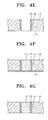
- FIGS. 4A through 4G are views illustrating the processes for fabricating the wiring structure of FIG. 2;
- FIGS. 5A through 5H are sectional views illustrating the processes for fabricating the protecting cap for the device package of FIG. 3.
- FIG. 2 shows a wiring structure 100 according to an embodiment of the present invention.
- a via-hole 111 is formed on the substrate 110.
- a buffer layer 113 is formed on an inner surface of the via-hole 111 and a plating layer 115 fills the via hole inside of the buffer layer 113.
- the buffer layer 113 compensates for a difference in thermal expansion coefficient between the substrate 110 made of silicon (Si) and the plating layer 115 made of a conductive metal.
- the buffer layer 113 can comprise PARYLENE or photoresist as the polymer which is an insulator.
- the photoresist may comprise polymer such as Novolak resin.
- FIG. 3 illustrates the wiring structure 100 of FIG. 2 mating to a protecting cap 200 for providing a device package.
- a device 301 is mounted on a surface of a device substrate 310, and a protecting cap 200 is connected to an external electrode to protect the device 301 from external impact.
- the protecting cap 200 includes a packaging substrate 210 having at one side thereof a space 211 for receiving the device 301.
- a lower electrode layer 230 is formed on a first side, having the space 211, of the packaging substrate 210.
- the lower electrode layer 230 is connected to a device electrode layer 320 formed on the device substrate 310.
- a via-hole 213 is formed in the packaging substrate 210 and a buffer layer 250 is formed on an inner surface of the via-hole 213.
- a plating layer 270 made of conductive metal fills the via hole inside of the buffer layer 250.
- an upper electrode layer 280 is formed on the packaging substrate 210 in connection with the plating layer 270.
- a driving signal can be transmitted to the device 301.
- a packaging bonding layer 290 is additionally deposited on a lower surface of the lower electrode layer 230 and bonded to a device bonding layer 350 formed on the device substrate 310.
- the device 301 can be protected from the external environment.
- the buffer layer 250 compensates for a difference in thermal expansion coefficient between the packaging substrate 210 and the plating layer 270. Therefore, when performing a reliability test in a high temperature environment, breakage or damage to the packaging substrate 210, which may be generated due to the difference in thermal expansion coefficient, can be prevented
- the buffer layer 250 isolates the upper electrode layer 280 and the packaging substrate 210.
- FIGS. 4A through 4G are views illustrating the processes for fabricating the wiring structure 100 of FIG. 2.
- FIG. 4A shows the substrate 110 which may be made of silicon (Si).
- a metal layer 114 is deposited for use as a seed layer for electrolytic plating or non-electrolytic plating of the plating layer 115.
- the metal layer 114 may comprise a conductive metal.
- the substrate 110 is etched by an etching device to form the via-hole 111 in a predetermined size.
- a buffer layer 113 is deposited on an upper surface of the substrate 110 having the via-hole 111.
- the buffer layer 113 may comprise an insulating polymer, more preferably PARYLENE or photoresist.
- PARYLENE can be deposited by evaporating with an evaporator, thermally decomposing in a thermal-decomposition area and supplying to a vacuum chamber, thereby adhering the PARYLENE to a substrate introduced into the vacuum chamber.
- a spin coater When depositing the photoresist, a spin coater can be used. More specifically, the substrate 110 is seated on a rotator and liquid photoresist is sprayed on an upper surface of the substrate 110 using a nozzle. The liquid photoresist is evenly coated on the substrate 110 by centrifugal force of the rotator, thereby forming a photoresist film. PARYLENE is preferably used because it forms a deposited film of more even thickness (conformal coating).
- horizontal planes S and S2 (FIG. 4D) of the buffer layer 113 are removed by reactive ion etching, so that only a vertical plane is left on an inner surface of the via-hole 111.
- a predetermined plating process such as electrolytic plating or non-electrolytic plating is performed so as to fill a plating layer 115 formed of conductive metal in the via-hole 111.
- the metal layer 114 serves as a plating seed layer.
- the wiring of substrate 110 is completed by removing metal layer 114.
- FIGS. 5A through 5H are sectional views illustrating a process for fabricating the protecting cap 200 of the device package of FIG. 3.
- FIG. 5A shows the packaging substrate 210 having at one side thereof a space 211 for receiving the device 301.
- the lower electrode layer 230 made of conductive metal is deposited on a first side of the packaging substrate 210, which has the space 211.
- the lower electrode layer 230 is connected to the device electrode layer 320 as shown in FIG. 3.
- a packaging bonding layer 290 is deposited for connecting with the device bonding layer 350 of FIG. 3. As well as the device bonding layer 350, the packaging bonding layer 290 functions as a sealing member.
- a via-hole 213 is etched in the packaging substrate 210 in a predetermined size by the etching device.
- a buffer layer 250 is deposited in a predetermined thickness on the upper surface of the packaging substrate 210 and on the inside of the via-hole 213.
- the buffer layer 250 can be formed using the same material and method as the buffer layer 113. Therefore, a detailed description thereof is provided by reference to the description of FIG. 4D.
- horizontal planes S 1 ' and S 2 ' (FIG. 5E) of the buffer layer 250 are removed by reactive ion etching, so that only a vertical plane formed on an inner surface of the via-hole 111 rerimains.
- a predetermined plating process such as electrolytic plating or non-electrolytic plating is performed so as to fill a plating layer 270 formed of conductive metal in the via-hole 213.
- the lower electrode layer 230 serves as a plating seed layer.
- an upper electrode layer 280 is deposited on the upper surface of the packaging substrate 210 so as to connect with the lower electrode layer 230 via the plating layer 270.
- the buffer layer 250 is arranged between the packaging substrate 210 and the plating layer 270 to compensate for a difference in thermal expansion coefficient between the plating layer 270 and the packaging substrate 210, and such structure is applied to the protecting cap 200 for providing a device package.
- the above structure is also applicable to an interlayer wiring structure comprising multi-layers.
Landscapes
- Engineering & Computer Science (AREA)
- Microelectronics & Electronic Packaging (AREA)
- Physics & Mathematics (AREA)
- Condensed Matter Physics & Semiconductors (AREA)
- General Physics & Mathematics (AREA)
- Computer Hardware Design (AREA)
- Power Engineering (AREA)
- Internal Circuitry In Semiconductor Integrated Circuit Devices (AREA)
- Printing Elements For Providing Electric Connections Between Printed Circuits (AREA)
Applications Claiming Priority (1)
| Application Number | Priority Date | Filing Date | Title |
|---|---|---|---|
| KR1020040083856A KR20060034850A (ko) | 2004-10-20 | 2004-10-20 | 배선 장치, 이를 이용한 디바이스 패키지용 보호 캡,그리고 그것들을 제조하기 위한 방법 |
Publications (1)
| Publication Number | Publication Date |
|---|---|
| EP1650797A2 true EP1650797A2 (de) | 2006-04-26 |
Family
ID=35673348
Family Applications (1)
| Application Number | Title | Priority Date | Filing Date |
|---|---|---|---|
| EP05019681A Withdrawn EP1650797A2 (de) | 2004-10-20 | 2005-09-09 | Verdrahtungsvorrichtung, Schutzkappe für Gehäuse für Bauelemente und zugehörige Herstellungsmethode |
Country Status (4)
| Country | Link |
|---|---|
| US (1) | US20060083904A1 (de) |
| EP (1) | EP1650797A2 (de) |
| JP (1) | JP2006121080A (de) |
| KR (1) | KR20060034850A (de) |
Cited By (4)
| Publication number | Priority date | Publication date | Assignee | Title |
|---|---|---|---|---|
| GB2427964A (en) * | 2005-06-30 | 2007-01-10 | Avago Technologies Wireless Ip | Wafer level packaging of FBAR chips |
| WO2009089996A1 (en) * | 2008-01-15 | 2009-07-23 | Hymite A/S | Fabrication of compact semiconductor packages |
| EP2365741A1 (de) * | 2010-03-10 | 2011-09-14 | Commissariat à l'Énergie Atomique et aux Énergies Alternatives | Verfahren zur Metallisierung von Blindlöchern |
| US8263491B2 (en) | 2006-10-20 | 2012-09-11 | Infineon Technologies Ag | Substrate with feedthrough and method for producing the same |
Families Citing this family (2)
| Publication number | Priority date | Publication date | Assignee | Title |
|---|---|---|---|---|
| KR100599088B1 (ko) * | 2005-06-20 | 2006-07-12 | 삼성전자주식회사 | 반도체 소자 패키지용 캡 및 그 제조방법 |
| CN110831336B (zh) * | 2019-11-11 | 2020-10-27 | 珠海崇达电路技术有限公司 | 一种大孔径背钻孔的树脂塞孔方法 |
-
2004
- 2004-10-20 KR KR1020040083856A patent/KR20060034850A/ko not_active Application Discontinuation
-
2005
- 2005-09-09 EP EP05019681A patent/EP1650797A2/de not_active Withdrawn
- 2005-10-17 JP JP2005301755A patent/JP2006121080A/ja not_active Withdrawn
- 2005-10-19 US US11/252,588 patent/US20060083904A1/en not_active Abandoned
Cited By (7)
| Publication number | Priority date | Publication date | Assignee | Title |
|---|---|---|---|---|
| GB2427964A (en) * | 2005-06-30 | 2007-01-10 | Avago Technologies Wireless Ip | Wafer level packaging of FBAR chips |
| GB2427964B (en) * | 2005-06-30 | 2009-05-27 | Avago Technologies Wireless Ip | A method for the wafer level packaging of FBAR chips,and a device package |
| US8263491B2 (en) | 2006-10-20 | 2012-09-11 | Infineon Technologies Ag | Substrate with feedthrough and method for producing the same |
| WO2009089996A1 (en) * | 2008-01-15 | 2009-07-23 | Hymite A/S | Fabrication of compact semiconductor packages |
| EP2365741A1 (de) * | 2010-03-10 | 2011-09-14 | Commissariat à l'Énergie Atomique et aux Énergies Alternatives | Verfahren zur Metallisierung von Blindlöchern |
| FR2957480A1 (fr) * | 2010-03-10 | 2011-09-16 | Commissariat Energie Atomique | Procede de metallisation de vias borgnes |
| US9003654B2 (en) | 2010-03-10 | 2015-04-14 | Commissariat à l'énergie atomique et aux énergies alternatives | Method for metalizing blind vias |
Also Published As
| Publication number | Publication date |
|---|---|
| US20060083904A1 (en) | 2006-04-20 |
| JP2006121080A (ja) | 2006-05-11 |
| KR20060034850A (ko) | 2006-04-26 |
Similar Documents
| Publication | Publication Date | Title |
|---|---|---|
| US20230420313A1 (en) | Seal for microelectronic assembly | |
| US8324736B2 (en) | Manufacturing process and structure of through silicon via | |
| KR100840502B1 (ko) | 반도체 장치 및 그 제조 방법 | |
| US8349733B2 (en) | Manufacturing method of substrate with through electrode | |
| US7008817B2 (en) | Method for manufacturing micro electro-mechanical systems using solder balls | |
| US20040224499A1 (en) | Semiconductor device substrate and manufacturing method thereof and semiconductor package | |
| US9349673B2 (en) | Substrate, method of manufacturing substrate, semiconductor device, and electronic apparatus | |
| EP2291858B1 (de) | Verkapseltes halbleiterprodukt und verfahren zu seiner herstellung | |
| US20060022325A1 (en) | Cap wafer, semiconductor package, and fabricating method thereof | |
| WO2005059998A1 (en) | Integrated circuits and packaging substrates with cavities, and attachment methods including insertion of protruding contact pads into cavities | |
| WO2012011931A1 (en) | Microelectronic elements having metallic pads overlying vias | |
| JP3975194B2 (ja) | パッケージの製造方法 | |
| US8053807B2 (en) | Semiconductor packages, stacked semiconductor packages, and methods of manufacturing the semiconductor packages and the stacked semiconductor packages | |
| US7786573B2 (en) | Packaging chip having interconnection electrodes directly connected to plural wafers | |
| US20100108361A1 (en) | Wiring substrate and method of manufacturing the wiring substrate | |
| US8872334B2 (en) | Method for manufacturing semiconductor device | |
| EP1650797A2 (de) | Verdrahtungsvorrichtung, Schutzkappe für Gehäuse für Bauelemente und zugehörige Herstellungsmethode | |
| WO2014130959A1 (en) | Carrier-less silicon interposer | |
| US20040195669A1 (en) | Integrated circuit packaging apparatus and method | |
| TWI395318B (zh) | 使用嵌入式晶片載板之薄型立體堆疊封裝結構 | |
| US11183483B2 (en) | Multichip module and electronic device | |
| CN114883251A (zh) | 一种直孔硅通孔的介质层填充方法 | |
| WO2011105961A1 (en) | Method of stacking chips | |
| US20040089930A1 (en) | Simplified stacked chip assemblies | |
| CN118108178A (zh) | 一种mems器件的封装方法及mems器件 |
Legal Events
| Date | Code | Title | Description |
|---|---|---|---|
| PUAI | Public reference made under article 153(3) epc to a published international application that has entered the european phase |
Free format text: ORIGINAL CODE: 0009012 |
|
| 17P | Request for examination filed |
Effective date: 20050909 |
|
| AK | Designated contracting states |
Kind code of ref document: A2 Designated state(s): AT BE BG CH CY CZ DE DK EE ES FI FR GB GR HU IE IS IT LI LT LU LV MC NL PL PT RO SE SI SK TR |
|
| AX | Request for extension of the european patent |
Extension state: AL BA HR MK YU |
|
| STAA | Information on the status of an ep patent application or granted ep patent |
Free format text: STATUS: THE APPLICATION HAS BEEN WITHDRAWN |
|
| 18W | Application withdrawn |
Effective date: 20060718 |