EP1646092A2 - Contact and omni directional reflective mirror for flip chipped light emitting devices - Google Patents
Contact and omni directional reflective mirror for flip chipped light emitting devices Download PDFInfo
- Publication number
- EP1646092A2 EP1646092A2 EP05108919A EP05108919A EP1646092A2 EP 1646092 A2 EP1646092 A2 EP 1646092A2 EP 05108919 A EP05108919 A EP 05108919A EP 05108919 A EP05108919 A EP 05108919A EP 1646092 A2 EP1646092 A2 EP 1646092A2
- Authority
- EP
- European Patent Office
- Prior art keywords
- layer
- conductivity type
- light emitting
- emitting device
- vias
- Prior art date
- Legal status (The legal status is an assumption and is not a legal conclusion. Google has not performed a legal analysis and makes no representation as to the accuracy of the status listed.)
- Granted
Links
Images

Classifications
-
- H—ELECTRICITY
- H10—SEMICONDUCTOR DEVICES; ELECTRIC SOLID-STATE DEVICES NOT OTHERWISE PROVIDED FOR
- H10H—INORGANIC LIGHT-EMITTING SEMICONDUCTOR DEVICES HAVING POTENTIAL BARRIERS
- H10H20/00—Individual inorganic light-emitting semiconductor devices having potential barriers, e.g. light-emitting diodes [LED]
- H10H20/80—Constructional details
- H10H20/83—Electrodes
- H10H20/831—Electrodes characterised by their shape
-
- H—ELECTRICITY
- H10—SEMICONDUCTOR DEVICES; ELECTRIC SOLID-STATE DEVICES NOT OTHERWISE PROVIDED FOR
- H10H—INORGANIC LIGHT-EMITTING SEMICONDUCTOR DEVICES HAVING POTENTIAL BARRIERS
- H10H20/00—Individual inorganic light-emitting semiconductor devices having potential barriers, e.g. light-emitting diodes [LED]
- H10H20/01—Manufacture or treatment
-
- H—ELECTRICITY
- H10—SEMICONDUCTOR DEVICES; ELECTRIC SOLID-STATE DEVICES NOT OTHERWISE PROVIDED FOR
- H10H—INORGANIC LIGHT-EMITTING SEMICONDUCTOR DEVICES HAVING POTENTIAL BARRIERS
- H10H20/00—Individual inorganic light-emitting semiconductor devices having potential barriers, e.g. light-emitting diodes [LED]
- H10H20/80—Constructional details
- H10H20/83—Electrodes
- H10H20/832—Electrodes characterised by their material
- H10H20/835—Reflective materials
-
- H—ELECTRICITY
- H10—SEMICONDUCTOR DEVICES; ELECTRIC SOLID-STATE DEVICES NOT OTHERWISE PROVIDED FOR
- H10H—INORGANIC LIGHT-EMITTING SEMICONDUCTOR DEVICES HAVING POTENTIAL BARRIERS
- H10H20/00—Individual inorganic light-emitting semiconductor devices having potential barriers, e.g. light-emitting diodes [LED]
- H10H20/01—Manufacture or treatment
- H10H20/032—Manufacture or treatment of electrodes
-
- H—ELECTRICITY
- H10—SEMICONDUCTOR DEVICES; ELECTRIC SOLID-STATE DEVICES NOT OTHERWISE PROVIDED FOR
- H10H—INORGANIC LIGHT-EMITTING SEMICONDUCTOR DEVICES HAVING POTENTIAL BARRIERS
- H10H20/00—Individual inorganic light-emitting semiconductor devices having potential barriers, e.g. light-emitting diodes [LED]
- H10H20/80—Constructional details
- H10H20/81—Bodies
- H10H20/819—Bodies characterised by their shape, e.g. curved or truncated substrates
-
- H—ELECTRICITY
- H10—SEMICONDUCTOR DEVICES; ELECTRIC SOLID-STATE DEVICES NOT OTHERWISE PROVIDED FOR
- H10H—INORGANIC LIGHT-EMITTING SEMICONDUCTOR DEVICES HAVING POTENTIAL BARRIERS
- H10H20/00—Individual inorganic light-emitting semiconductor devices having potential barriers, e.g. light-emitting diodes [LED]
- H10H20/80—Constructional details
- H10H20/83—Electrodes
- H10H20/832—Electrodes characterised by their material
- H10H20/833—Transparent materials
Definitions
- the present invention relates generally to light emitting diodes and more specifically to contacts for light emitting diodes.
- LEDs light emitting diodes
- III-V semiconductors particularly binary, ternary, and quaternary alloys of gallium, aluminum, indium, and nitrogen, also referred to as III-nitride materials; and binary, ternary, and quaternary alloys of gallium, aluminum, indium, and phosphorus, also referred to as III-phosphide materials.
- III-nitride devices are epitaxially grown on sapphire, silicon carbide, or III-nitride substrates and III-phosphide devices are epitaxially grown on gallium arsenide by metal organic chemical vapor deposition (MOCVD) molecular beam epitaxy (MBE) or other epitaxial techniques.
- MOCVD metal organic chemical vapor deposition
- MBE molecular beam epitaxy
- These LED device structures can also be transferred to a transparent substrate by wafer bonding.
- an n-type layer (or layers) is deposited on the substrate, then an active region is deposited on the n-type layers, then a p-type layer (or layers) is deposited on the active region. The order of the layers may be reversed such that the p-type layers are adjacent to the substrate by either epitaxial growth or wafer bonding.
- Fig. 1 illustrates a cross-sectional view of a conventional light emitting diode (LED) 10.
- LED light emitting diode
- one or more p type layers are formed over a substrate 12.
- a p-AlInP layer 16 may be formed over a p doped region 14 of a GaP substrate 10 by wafer bonding, and p-contacts 18 are formed on the p doped region 14.
- An active region 20 is formed over the p type layer 16 and an n type layer 22, e.g., an n-AIInP layer, is formed over the active region 20.
- An n contact 24 is formed over the n type layer 22, but the contact area is minimized in order to increase the area of the reflective mirror 26 area for better light extraction through the substrate 10.
- the LED 10 can be used in a flip chip configuration with the p-contacts 18 and n-contacts 24 formed on the same side of the device when flip-chipped on a submount and where the light is extracted through the substrate 12, which is the top of the device.
- the design scheme of the flip chip LED 10 forces lateral current injection, which results in current crowding under the n-contact 24 and near the p contact area 18 as illustrated by the arrows in Fig. 1.
- the current crowding results in non-uniform current injection as well as high series resistance and high forward voltage Vf compared to vertical injection LEDs.
- One manner of solving the non-uniform current injection problem in the n-side is to use full sheet n-metal contact.
- the n-metal contact has to be annealed at high temperature, e.g., greater than 420°C, to achieve a good ohmic contact, the metal surface is rough. As a result, the reflectively of the full sheet n-metal contact is poor and thus, decreases light extraction.
- a light emitting device includes a substrate, a doped substrate layer, a layer of first conductivity type overlying the doped substrate layer, a light emitting layer overlying the layer of first conductivity type, and a layer of second conductivity type overlying the light emitting layer.
- a conductive transparent film such as indium tin oxide, and a reflective metal layer overlie the layer of second conductivity type and provide electrical contact with the layer of second conductivity type.
- a plurality of vias may be formed in the reflective metal layer and conductive transparent film as well as the layer of second conductivity type, the light emitting layer and layer of first conductivity type, down to the doped substrate layer.
- a plurality of contacts is formed in the vias and is in electrical contact with the doped substrate layer.
- An insulating layer formed over the reflective metal layer insulates the plurality of contacts from the conductive transparent film and reflective metal layers.
- the use of the conductive transparent film, such as indium tin oxide layer and a reflective metal layer together is particularly advantageous as it provides high reflection for the light over all incident angles.
- the conductive transparent film provides a uniform current injection from one side of the active region, eliminating the current crowding problem at the n-layer found in conventional devices.
- a distributed array of vias and contacts through the conductive transparent film and reflective metal layer and the layer of second conductivity type, the light emitting layer and layer of first conductivity type to the underlying doped substrate layer improves current spreading from the other side of the active region as well as increases the junction area of the device.
- Fig 2 illustrates a cross sectional view of an light emitting device (LED) 100, in accordance with one embodiment of the present invention, that uses a full sheet contact with an omni directional high reflective mirror (ODRM) structure 101.
- LED light emitting device
- ODRM omni directional high reflective mirror
- LED 100 includes one or more p-type layers 106 formed over a substrate 102.
- the p-type layer 106 e.g., may be P-AlInP layers formed over a p doped GaP layer 104 that is bonded to an undoped GaP substrate 102.
- the p contacts 105 which may be formed from, e.g., AuZn, are formed over the p doped GaP layer 104.
- An active region 108 is formed over the p type layer 106 and an n type layer 110, e.g., n-AIInP, is formed over the active region 108.
- the LED 100 may include one or more capping layers 112, e.g., of n+GaAs and/or n+InGaP over the n type layer 110.
- the ODRM structure 101 is formed over the capping layers 112 from a full sheet conductive transparent film 114 of, e.g., indium tin oxide (ITO), and a high reflective mirror 116 of, e.g., Ag or Au.
- transparent is used herein to indicate that an optical element so described, such as a “transparent film,” a “transparent layer,” or a “transparent substrate,” transmits light at the emission wavelengths of the LED with less than about 50%, preferably less than about 10%, single pass loss due to absorption or scattering.
- the conductive transparent film 114 is sometimes referred to herein as an ITO layer 114, but it should be understood that other conductive and transparent films may be used.
- the conductive transparent film 114 serves as the n contact for the LED 100 and the mirror 116 overlies the conductive transparent film 114.
- the ITO layer 114 has a thickness that is, e.g., a quarter of the wavelength produced by the LED 100.
- the ITO layer 114 is approximately 73 nm thick at a wavelength of 615nm and has a refractive index of 2.1.
- the contact resistance of the ITO layer 114 is expected to be 1.5e-5 ⁇ cm 2 or lower, with a transmission of approximately 95% or better around 600nm.
- the ODMR structure 101 provides high reflection for the light reaching the ODMR structure 101 over all incident angles.
- the ODRM structure 101 with a quarter wavelength ITO layer 114 and an Ag mirror 116 is expected to have a reflectively of over 90% for a wide range of incident angles.
- using the ITO layer 114 as a full sheet n-contact provides a uniform current injection from the n-side into the active region 108, eliminating the current crowding problem at the n-layer 110 found in conventional devices. Accordingly, the ODMR structure 101 reduces the forward voltage Vf and series resistance while increasing the extraction efficiency of the LED 100 compared to conventional devices.
- the LED 100 of the present embodiment is described as a flip chip AlInGaP type device, the present ODRM structure may be used with difference devices if desired.
- the ODRM structure may be used with a flip chip InGaN LED devices.
- the ITO layer 114 can be used as a transparent contact on a p-GaN layer.
- the ITO layer 114 can also be applied on top of p-GaAs or P-InGaN contact layers.
- a uniform current injection is provided at the n side of the active region.
- the current injection at the p side of the active region may still be problematic due to the lateral contact scheme in a wide mesa structure such as that shown in Fig. 2.
- four mesas are conventionally formed by etching to the p-GaP contact layer.
- the spacing between the p-contact and the center of the mesa for such a structure is over 100 ⁇ m. Due to the poor conductivity of the p-GaP, the hole injection on the p-side of the active region is not uniform across the mesa. Accordingly, current crowding may occur around the edges of the mesa.
- a distributed p-contact array is used, along with the ODRM structure 101, to improve current spreading and increase the junction area of the LED.
- the distributed contact array may be similar to that disclosed in U.S. 2003/0230754, entitled “Contacting Scheme for Large and Small Area Semiconductor Light Emitting Flip-Chip Devices", by Daniel A. Steigerwald et al., filed June 13, 2002, which has the same assignee as the present disclosure and is incorporated herein by reference.
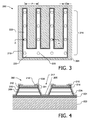
- Fig. 3 illustrates a top view of an LED 200 with an ODRM structure 201 that serves as the n-contact, and a distributed p-contact array, in accordance with an embodiment of the present invention.
- Fig. 4 illustrates a cross sectional view of a portion of LED 200 along line A-A in Fig. 3.
- LED 200 includes one or more p-type layers 206 formed over p-doped layer 204 that is bonded to a substrate 202.
- the p-doped layer 204 may be, e.g., 2 to 20 ⁇ m of p-GaP that is optimized for good current spreading.
- the thicker the p-doped layer 204 the larger the p-contact array spacing can be for uniform current spreading.
- a thicker p-doped layer 204 increases light absorption loss. Therefore, the p-doped layer 204 should be kept as thin as possible with a small p-contact array pitch for uniform current spreading.
- the ODRM 201 is formed over the capping layer 212 as a conductive transparent film 214, such as a quarter wavelength thick ITO layer 214, and an Ag or Au reflective mirror 216 formed over the ITO layer 214.
- the LED 200 may be mounted to a submount (not shown) of silicon or ceramic and the cathode and the anode of the LED 200 can be connected to the corresponding contact pads on the submount through solder bumps or Au-Au stud bumps.
- the p-contact 205 is formed as a distributed array 116 by etching several vias 217 down to the p doped layer 204, by etching away the ODRM 201, the capping layer 212, the n-type layer 210, the active region 208 and the p-type layer 206 with, for example, a reactive ion etch; by ion implantation; by dopant diffusion; or by selective growth of the layers.
- the p-doped layer 204 is exposed for the p contact 205.
- the p-contacts 205 in the distributed array 216 are connected together by interconnect 222, which is formed by the p contact layer 220, as illustrated in Fig. 3.
- the dielectric layer 218 isolates the p contact layer 220 from the reflective mirror 216 and ITO layer 214 in the ODRM 201.
- a 4x4 distributed p-contact array such as that shown in Fig. 3, is formed by etching vias 217 through the device and into the p-GaP layer 204 and depositing an AuZn p-contact layer 220 into the vias 217.
- the via pitch (dimension P in Fig. 3) may be, for example, about 50 ⁇ m to about 1000 ⁇ m, and is usually about 50 ⁇ m to about 200 ⁇ m.
- the via diameter (dimension D in Fig. 3) may be, for example, between about 2 ⁇ m and about 100 ⁇ m and is usually between about 10 ⁇ m and about 50 ⁇ m.
- the farthest current conduction path for holes is approximately 37.5 ⁇ m, which is the distance from the edge of a p-contact 205 to the center of two adjacent p-contacts 205 and approximately 58 ⁇ m on the diagonally between p contacts 205. Moreover, the total junction area is approximately 96 percent.
- a conventional LED of the same size with dual mesas and stripped p-contacts has a junction of approximately 75 percent assuming the mesa width is approximately 210 ⁇ m, the p-contact line around the mesa is 20 ⁇ m wide and the solder metal pad is 50 ⁇ m in diameter.
- FIG. 3 has a 4x4 rectangular array of vias, a rectangular array of a different size (for example, 6x6 or 9x9) may also be used, as well as a hexagonal array, a rhombohedral array, a face-centered cubic array, an arbitrary arrangement, or any other suitable arrangement.
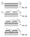
- Figs. 5A-5D illustrate an embodiment of the present invention at various stages during fabrication.
- Layers 212, 210, 208, 206, and 204, shown in Fig. 5A are epitaxially grown on an n-GaAs substrate (not shown) and then bonded to GaP substrate 202.
- the capping layer 212 e.g., of n+GaAs or n+InGaP, is formed over the n-GaAs substrate.
- One or more n-type layers 210 are formed on the capping layer 212.
- N-type layers 210 may include, for example, a buffer layer, a contact layer, an undoped crystal layer, and n-type layers of varying composition and dopant concentration.
- An active region 208 is then formed on the n-type layers 210.
- Active region 208 may include, for example, a set of quantum well layers separated by a set of barrier layers.
- One or more p-type layers 206 are formed on the active region 208.
- P-type layers 206 may include, for example, may include, for example, a carrier confining layer, a contact layer, and other p-type layers of various composition and dopant concentration.
- the various layers may be deposited by, for example, MOCVD or other appropriate, well known techniques.
- the p-type layers 206 are then bonded to the GaP substrate 202 and the n-GaAs substrate is selectively removed.
- the ITO layer 214 is deposited over the capping layer 212 and the reflective mirror layer 216 of, e.g., Ag or Au, is deposited over the ITO layer 214 resulting in the structure shown in Fig. 5A.
- the ITO layer 214 and the reflective mirror layer 216 may be deposited by, e.g., e-beam evaporation or sputtering.
- the ITO layer 214, mirror layer 216 and the capping layer 212 are patterned as shown in Fig. 5B, using for example photolithography along with etching, or a lift-off process.
- the patterning removes any of the ITO layer 214, mirror layer 216 and capping layer 212 that will not be used as an n-contact.
- the patterning thus removes any of the n contact overlying vias 217 shown in Figs. 3 and 4.
- one or more etching steps are then performed to form vias 217.
- Dielectric layer 218 may be any material that electrically isolates two materials on either side of dielectric layer 218.
- Dielectric layer 218 is patterned to remove a portion of the dielectric material covering the p layer 204 at the bottom of via 217 and a portion of the top of the mirror layer 216.
- Dielectric layer 218 must have a low density of pinholes to prevent short-circuiting between the p- and n-contacts. In some embodiments, dielectric layer 218 is multiple dielectric layers.
- the p contact layer 220 is then deposited over the dielectric layer 218 and in via 217.
- the interconnect 222 which connects the p-metal deposited in each via 217, may also be deposited at this time.
- the p contact layer 220 is patterned to remove a portion of the material covering the mirror layer 216 as shown in Fig. 4.
Landscapes
- Led Devices (AREA)
- Electroluminescent Light Sources (AREA)
Abstract
Description
- The present invention relates generally to light emitting diodes and more specifically to contacts for light emitting diodes.
- Semiconductor light emitting devices such as light emitting diodes (LEDs) are among the most efficient light sources currently available. Material systems currently of interest in the manufacture of high brightness LEDs capable of operation across the visible spectrum include group III-V semiconductors, particularly binary, ternary, and quaternary alloys of gallium, aluminum, indium, and nitrogen, also referred to as III-nitride materials; and binary, ternary, and quaternary alloys of gallium, aluminum, indium, and phosphorus, also referred to as III-phosphide materials. Often III-nitride devices are epitaxially grown on sapphire, silicon carbide, or III-nitride substrates and III-phosphide devices are epitaxially grown on gallium arsenide by metal organic chemical vapor deposition (MOCVD) molecular beam epitaxy (MBE) or other epitaxial techniques. These LED device structures can also be transferred to a transparent substrate by wafer bonding. Often, an n-type layer (or layers) is deposited on the substrate, then an active region is deposited on the n-type layers, then a p-type layer (or layers) is deposited on the active region. The order of the layers may be reversed such that the p-type layers are adjacent to the substrate by either epitaxial growth or wafer bonding.
- Fig. 1 illustrates a cross-sectional view of a conventional light emitting diode (LED) 10. As shown in Fig. 1, one or more p type layers are formed over a
substrate 12. By way of example, a p-AlInP layer 16 may be formed over a p dopedregion 14 of aGaP substrate 10 by wafer bonding, and p-contacts 18 are formed on the p dopedregion 14. Anactive region 20 is formed over thep type layer 16 and ann type layer 22, e.g., an n-AIInP layer, is formed over theactive region 20. Ann contact 24 is formed over then type layer 22, but the contact area is minimized in order to increase the area of thereflective mirror 26 area for better light extraction through thesubstrate 10. Thus, theLED 10 can be used in a flip chip configuration with the p-contacts 18 and n-contacts 24 formed on the same side of the device when flip-chipped on a submount and where the light is extracted through thesubstrate 12, which is the top of the device. - The design scheme of the
flip chip LED 10 forces lateral current injection, which results in current crowding under the n-contact 24 and near thep contact area 18 as illustrated by the arrows in Fig. 1. The current crowding results in non-uniform current injection as well as high series resistance and high forward voltage Vf compared to vertical injection LEDs. - One manner of solving the non-uniform current injection problem in the n-side is to use full sheet n-metal contact. However, because the n-metal contact has to be annealed at high temperature, e.g., greater than 420°C, to achieve a good ohmic contact, the metal surface is rough. As a result, the reflectively of the full sheet n-metal contact is poor and thus, decreases light extraction.
- Thus, it is highly desirable to improve the contacts used with LEDs reduce the non-uniform current injection problem without decreasing light extraction.
- In accordance with one embodiment of the present invention, a light emitting device includes a substrate, a doped substrate layer, a layer of first conductivity type overlying the doped substrate layer, a light emitting layer overlying the layer of first conductivity type, and a layer of second conductivity type overlying the light emitting layer. A conductive transparent film, such as indium tin oxide, and a reflective metal layer overlie the layer of second conductivity type and provide electrical contact with the layer of second conductivity type. In one embodiment, a plurality of vias may be formed in the reflective metal layer and conductive transparent film as well as the layer of second conductivity type, the light emitting layer and layer of first conductivity type, down to the doped substrate layer. A plurality of contacts is formed in the vias and is in electrical contact with the doped substrate layer. An insulating layer formed over the reflective metal layer insulates the plurality of contacts from the conductive transparent film and reflective metal layers.
- The use of the conductive transparent film, such as indium tin oxide layer and a reflective metal layer together is particularly advantageous as it provides high reflection for the light over all incident angles. Moreover, the conductive transparent film provides a uniform current injection from one side of the active region, eliminating the current crowding problem at the n-layer found in conventional devices. Further, a distributed array of vias and contacts through the conductive transparent film and reflective metal layer and the layer of second conductivity type, the light emitting layer and layer of first conductivity type to the underlying doped substrate layer improves current spreading from the other side of the active region as well as increases the junction area of the device.
-
- Fig. 1 illustrates a cross-sectional view of a conventional light emitting diode.
- Fig 2 illustrates a cross sectional view of a light emitting device that uses a full sheet contact with an omni directional high reflective mirror (ODRM) structure, in accordance with one embodiment of the present invention.
- Fig. 3 illustrates a top view of a light-emitting device with an ODRM structure and a distributed p-contact array, in accordance with another embodiment of the present invention.
- Fig. 4 illustrates a cross sectional view of a portion of light emitting device from Fig. 3 along line A-A.
- Figs. 5A-5D illustrate an embodiment of the present invention at various stages during fabrication.
- Fig 2 illustrates a cross sectional view of an light emitting device (LED) 100, in accordance with one embodiment of the present invention, that uses a full sheet contact with an omni directional high reflective mirror (ODRM) structure 101.
- As shown in Fig. 2,
LED 100 includes one or more p-type layers 106 formed over asubstrate 102. The p-type layer 106, e.g., may be P-AlInP layers formed over a p dopedGaP layer 104 that is bonded to anundoped GaP substrate 102. Thep contacts 105, which may be formed from, e.g., AuZn, are formed over the p dopedGaP layer 104. Anactive region 108 is formed over thep type layer 106 and ann type layer 110, e.g., n-AIInP, is formed over theactive region 108. TheLED 100 may include one or more capping layers 112, e.g., of n+GaAs and/or n+InGaP over then type layer 110. - The ODRM structure 101 is formed over the capping layers 112 from a full sheet conductive transparent film 114 of, e.g., indium tin oxide (ITO), and a high
reflective mirror 116 of, e.g., Ag or Au. The term "transparent" is used herein to indicate that an optical element so described, such as a "transparent film," a "transparent layer," or a "transparent substrate," transmits light at the emission wavelengths of the LED with less than about 50%, preferably less than about 10%, single pass loss due to absorption or scattering. One of ordinary skill in the art will recognize that the conditions "less than 50% single pass loss" and "less than 10% single pass loss" may be met by various combinations of transmission path length and absorption constant. The conductive transparent film 114 is sometimes referred to herein as an ITO layer 114, but it should be understood that other conductive and transparent films may be used. The conductive transparent film 114 serves as the n contact for theLED 100 and themirror 116 overlies the conductive transparent film 114. Where indium tin oxide is used as the conductive transparent film 114, the ITO layer 114 has a thickness that is, e.g., a quarter of the wavelength produced by theLED 100. By example, the ITO layer 114 is approximately 73 nm thick at a wavelength of 615nm and has a refractive index of 2.1. The contact resistance of the ITO layer 114 is expected to be 1.5e-5 Ω cm2 or lower, with a transmission of approximately 95% or better around 600nm. - The ODMR structure 101 provides high reflection for the light reaching the ODMR structure 101 over all incident angles. For example, the ODRM structure 101 with a quarter wavelength ITO layer 114 and an
Ag mirror 116 is expected to have a reflectively of over 90% for a wide range of incident angles. Moreover, using the ITO layer 114 as a full sheet n-contact provides a uniform current injection from the n-side into theactive region 108, eliminating the current crowding problem at the n-layer 110 found in conventional devices. Accordingly, the ODMR structure 101 reduces the forward voltage Vf and series resistance while increasing the extraction efficiency of theLED 100 compared to conventional devices. - It should be understood that, while the
LED 100 of the present embodiment is described as a flip chip AlInGaP type device, the present ODRM structure may be used with difference devices if desired. For example, the ODRM structure may be used with a flip chip InGaN LED devices. It has been demonstrated that the ITO layer 114 can be used as a transparent contact on a p-GaN layer. The ITO layer 114 can also be applied on top of p-GaAs or P-InGaN contact layers. - With the use of the ODRM structure 101, a uniform current injection is provided at the n side of the active region. The current injection at the p side of the active region, however, may still be problematic due to the lateral contact scheme in a wide mesa structure such as that shown in Fig. 2. By way of example, for a 1mm x 1mm square red flip chip die, four mesas are conventionally formed by etching to the p-GaP contact layer. The spacing between the p-contact and the center of the mesa for such a structure is over 100µm. Due to the poor conductivity of the p-GaP, the hole injection on the p-side of the active region is not uniform across the mesa. Accordingly, current crowding may occur around the edges of the mesa.
- Thus, in accordance with another embodiment of the present invention, a distributed p-contact array is used, along with the ODRM structure 101, to improve current spreading and increase the junction area of the LED. The distributed contact array may be similar to that disclosed in U.S. 2003/0230754, entitled "Contacting Scheme for Large and Small Area Semiconductor Light Emitting Flip-Chip Devices", by Daniel A. Steigerwald et al., filed June 13, 2002, which has the same assignee as the present disclosure and is incorporated herein by reference.
- Fig. 3 illustrates a top view of an
LED 200 with anODRM structure 201 that serves as the n-contact, and a distributed p-contact array, in accordance with an embodiment of the present invention. Fig. 4 illustrates a cross sectional view of a portion ofLED 200 along line A-A in Fig. 3. - As can be seen in Fig. 4, the formation of
LED 200 is similar to that ofLED 100 shown in Fig. 2. For example,LED 200 includes one or more p-type layers 206 formed over p-dopedlayer 204 that is bonded to asubstrate 202. The p-dopedlayer 204 may be, e.g., 2 to 20µm of p-GaP that is optimized for good current spreading. In general, the thicker the p-dopedlayer 204, the larger the p-contact array spacing can be for uniform current spreading. A thicker p-dopedlayer 204, however, increases light absorption loss. Therefore, the p-dopedlayer 204 should be kept as thin as possible with a small p-contact array pitch for uniform current spreading. Over the p-type layer 206 is formed theactive region 208 and ann layer 210. Acapping layer 212 of, e.g., of n+GaAs and/or n+InGaP, is formed over then layer 210. TheODRM 201 is formed over thecapping layer 212 as a conductivetransparent film 214, such as a quarter wavelengththick ITO layer 214, and an Ag or Aureflective mirror 216 formed over theITO layer 214. TheLED 200 may be mounted to a submount (not shown) of silicon or ceramic and the cathode and the anode of theLED 200 can be connected to the corresponding contact pads on the submount through solder bumps or Au-Au stud bumps. - As illustrated in Fig. 3 and 4, however, the p-
contact 205 is formed as a distributedarray 116 by etchingseveral vias 217 down to the p dopedlayer 204, by etching away theODRM 201, thecapping layer 212, the n-type layer 210, theactive region 208 and the p-type layer 206 with, for example, a reactive ion etch; by ion implantation; by dopant diffusion; or by selective growth of the layers. Thus, the p-dopedlayer 204 is exposed for thep contact 205. Adielectric layer 218, such as SiNx or SiO2, is formed over the LED epi structure, i.e., layers 206, 208, 210, 212, and 201. Ap contact layer 220 of, e.g., AuZn, is formed over thedielectric layer 218 and is in electrical contact with the underlying p dopedlayer 204 to form thep contact 205. The p-contacts 205 in the distributedarray 216 are connected together byinterconnect 222, which is formed by thep contact layer 220, as illustrated in Fig. 3. Thedielectric layer 218 isolates thep contact layer 220 from thereflective mirror 216 andITO layer 214 in theODRM 201. - By way of example, for a 500µm x 500µm square LED chip, a 4x4 distributed p-contact array, such as that shown in Fig. 3, is formed by etching
vias 217 through the device and into the p-GaP layer 204 and depositing an AuZn p-contact layer 220 into thevias 217. The via pitch (dimension P in Fig. 3) may be, for example, about 50µm to about 1000µm, and is usually about 50µm to about 200µm. The via diameter (dimension D in Fig. 3) may be, for example, between about 2µm and about 100µm and is usually between about 10µm and about 50µm. Where the via pitch is 100µm and the via diameter is 25µm, the farthest current conduction path for holes is approximately 37.5µm, which is the distance from the edge of a p-contact 205 to the center of two adjacent p-contacts 205 and approximately 58µm on the diagonally betweenp contacts 205. Moreover, the total junction area is approximately 96 percent. By way of comparison, a conventional LED of the same size with dual mesas and stripped p-contacts has a junction of approximately 75 percent assuming the mesa width is approximately 210µm, the p-contact line around the mesa is 20µm wide and the solder metal pad is 50µm in diameter. - It should be understood, that the other dimensions or other materials may be used with the present invention if desired. Moreover, while the device illustrated in FIG. 3 has a 4x4 rectangular array of vias, a rectangular array of a different size (for example, 6x6 or 9x9) may also be used, as well as a hexagonal array, a rhombohedral array, a face-centered cubic array, an arbitrary arrangement, or any other suitable arrangement.
- Figs. 5A-5D illustrate an embodiment of the present invention at various stages during fabrication.
Layers GaP substrate 202. Thus, thecapping layer 212, e.g., of n+GaAs or n+InGaP, is formed over the n-GaAs substrate. One or more n-type layers 210 are formed on thecapping layer 212. N-type layers 210 may include, for example, a buffer layer, a contact layer, an undoped crystal layer, and n-type layers of varying composition and dopant concentration. Anactive region 208 is then formed on the n-type layers 210.Active region 208 may include, for example, a set of quantum well layers separated by a set of barrier layers. One or more p-type layers 206 are formed on theactive region 208. P-type layers 206 may include, for example, may include, for example, a carrier confining layer, a contact layer, and other p-type layers of various composition and dopant concentration. The various layers may be deposited by, for example, MOCVD or other appropriate, well known techniques. The p-type layers 206 are then bonded to theGaP substrate 202 and the n-GaAs substrate is selectively removed. TheITO layer 214 is deposited over thecapping layer 212 and thereflective mirror layer 216 of, e.g., Ag or Au, is deposited over theITO layer 214 resulting in the structure shown in Fig. 5A. TheITO layer 214 and thereflective mirror layer 216 may be deposited by, e.g., e-beam evaporation or sputtering. - The
ITO layer 214,mirror layer 216 and thecapping layer 212 are patterned as shown in Fig. 5B, using for example photolithography along with etching, or a lift-off process. The patterning removes any of theITO layer 214,mirror layer 216 andcapping layer 212 that will not be used as an n-contact. The patterning thus removes any of the ncontact overlying vias 217 shown in Figs. 3 and 4. As shown in Fig. 5C, one or more etching steps are then performed to formvias 217. - A
dielectric layer 218, such as for example silicon nitride or silicon oxide, is deposited, as shown in Fig. 5D to electrically isolate theITO layer 214 andmirror layer 216, which serve as the n-contact, from the p metal to be deposited in via 217.Dielectric layer 218 may be any material that electrically isolates two materials on either side ofdielectric layer 218.Dielectric layer 218 is patterned to remove a portion of the dielectric material covering thep layer 204 at the bottom of via 217 and a portion of the top of themirror layer 216.Dielectric layer 218 must have a low density of pinholes to prevent short-circuiting between the p- and n-contacts. In some embodiments,dielectric layer 218 is multiple dielectric layers. - The
p contact layer 220 is then deposited over thedielectric layer 218 and in via 217. Theinterconnect 222, which connects the p-metal deposited in each via 217, may also be deposited at this time. Thep contact layer 220 is patterned to remove a portion of the material covering themirror layer 216 as shown in Fig. 4. - Although the present invention is illustrated in connection with specific embodiments for instructional purposes, the present invention is not limited thereto. Various adaptations and modifications may be made without departing from the scope of the invention. Therefore, the spirit and scope of the appended claims should not be limited to the foregoing description.
Claims (28)
- A light emitting device comprising:a substrate;a layer of first conductivity type overlying the substrate;a light emitting layer overlying the layer of first conductivity type;a layer of second conductivity type overlying the light emitting layer;a conductive transparent layer overlying the layer of second conductivity type; anda reflective metal layer overlying the conductive transparent layer, wherein the conductive transparent layer and reflective metal layer provide electrical contact with the layer of a second conductivity type.
- The light emitting device of Claim 1, wherein the conductive transparent layer comprises indium tin oxide.
- The light emitting device of Claim 2, wherein the conductive transparent layer has a thickness that is approximately one quarter of the wavelength of the light produced by the light-emitting layer.
- The light emitting device of Claim 1, wherein the conductive transparent layer has a single pass loss of less than about 10%.
- The light emitting device of Claim 1, wherein the first conductivity type is a p type and the second conductivity type is an n type.
- The light emitting device of Claim 1, wherein the layer of first conductivity type and the layer of second conductivity type comprise aluminum, indium, and phosphorous.
- The light emitting device of Claim 1, wherein the layer of first conductivity type and the layer of second conductivity type comprise gallium and nitrogen.
- The light emitting device of Claim 1, wherein the layer of first conductivity type and the layer of second conductivity type comprise gallium and arsenic.
- The light emitting device of Claim 1, wherein the reflective metal layer comprises at least one of silver and gold.
- The light-emitting device of Claim 1, further comprising:a doped substrate layer of the first conductivity type underlying the layer of first conductivity type,a plurality of vias formed in the reflective metal layer, the conductive transparent layer, the layer of second conductivity type, the light emitting layer and the layer of first conductivity type, the plurality of vias extending to the doped substrate layer; anda plurality of contacts electrically contacting the doped substrate layer through the plurality of vias.
- The light emitting device of Claim 10, wherein each of the plurality of vias has a diameter ranging from about 2µm to about 100µm.
- The light emitting device of Claim 10, wherein each of the plurality of vias has a diameter ranging from about 10µm to about 50µm.
- The light emitting device of Claim 10, wherein each of the plurality of vias is located between about 50µm to about 1000µm from another via.
- The light emitting device of Claim 10, wherein each of the plurality of vias is located between about 50µm to about 250µm from another via.
- The light emitting device of Claim 10, wherein the plurality of vias are formed in an arrangement selected from the group consisting of rectangular, hexagonal, rhombohedral, face-centered cubic, and arbitrary.
- The light emitting device of Claim 10, further comprising: an insulating layer formed over the reflective metal layer and having a first plurality of openings aligned with the plurality of vias; and a plurality of interconnects formed over the insulating layer, the plurality of interconnects connecting the plurality of contacts.
- The light emitting device of Claim 16, wherein the insulating layer has a second plurality of openings over the reflective metal layer.
- A method of forming a light emitting device, the method comprising:providing a substrate;forming a layer of first conductivity type overlying the substrate;forming an active region overlying the layer of first conductivity type;forming a layer of second conductivity type overlying the active region;forming a conductive transparent layer overlying the layer of second conductivity type; andforming a reflective metal layer overlying the conductive transparent layer, wherein the conductive transparent layer and reflective metal layer provide electrical contact with the layer of a second conductivity type.
- The method of Claim 18, wherein the conductive transparent layer comprises indium tin oxide.
- The method of Claim 19, wherein the conductive transparent layer is formed with a thickness that is approximately one quarter of the wavelength of the light produced by the light emitting layer.
- The method of Claim 18, further comprising:forming a doped substrate layer of the first conductivity type between the substrate and the layer of first conductivity type;forming a plurality of vias in the reflective metal layer, conductive transparent layer, the layer of second conductivity type, the light emitting layer and the layer of first conductivity type, the plurality of vias contacting the layer of doped substrate layer;forming a plurality of contacts, the plurality of contacts contacting the doped substrate layer through the vias.
- The method of Claim 21, further comprising:forming an insulating layer over the reflective metal layer and producing a first plurality of openings aligned with the plurality of vias, the plurality of contacts being formed over the insulating layer; anda plurality of interconnects formed over the insulating layer, the plurality of interconnects connecting the plurality of contacts.
- The method of Claim 21, wherein forming a plurality of vias comprises etching away portions of the layer of second conductivity type, the light emitting layer and the layer of first conductivity type.
- A light emitting device comprising:a substrate;a doped substrate layer of first conductivity type overlying the substrate;a layer of the first conductivity type overlying the dopes substrate layer;a light emitting layer overlying the layer of first conductivity type;a layer of second conductivity type overlying the light emitting layer;a conductive transparent layer overlying the layer of second conductivity type;a reflective metal layer overlying the conductive transparent layer, wherein the conductive transparent layer and reflective metal layer provide electrical contact with the layer of a second conductivity type.a plurality of vias formed in the reflective metal layer, conductive transparent layer, layer of second conductivity type, the light emitting layer and the layer of first conductivity type, the plurality of vias extending to the doped substrate layer; an insulating layer formed over the reflective metal layer and having a first plurality of openings aligned with the plurality of vias and a second plurality of openings over the reflective metal layer; anda plurality of contacts electrically contacting the doped substrate layer through the plurality of vias.
- The light-emitting device of Claim 24, further comprising a plurality of interconnects formed over the insulating layer, the plurality of interconnects connecting the plurality of contacts.
- The light emitting device of Claim 24, wherein the conductive transparent layer comprises indium tin oxide.
- The light emitting device of Claim 26, wherein the conductive transparent layer has a thickness that is approximately one quarter of the wavelength of the light produced by the light-emitting layer.
- The light emitting device of Claim 24, wherein the reflective metal layer comprises at least one of silver and gold.
Applications Claiming Priority (1)
| Application Number | Priority Date | Filing Date | Title |
|---|---|---|---|
| US10/960,391 US7274040B2 (en) | 2004-10-06 | 2004-10-06 | Contact and omnidirectional reflective mirror for flip chipped light emitting devices |
Publications (3)
| Publication Number | Publication Date |
|---|---|
| EP1646092A2 true EP1646092A2 (en) | 2006-04-12 |
| EP1646092A3 EP1646092A3 (en) | 2006-12-06 |
| EP1646092B1 EP1646092B1 (en) | 2009-01-07 |
Family
ID=35636892
Family Applications (1)
| Application Number | Title | Priority Date | Filing Date |
|---|---|---|---|
| EP05108919A Expired - Lifetime EP1646092B1 (en) | 2004-10-06 | 2005-09-27 | Contact and omni directional reflective mirror for flip chipped light emitting devices |
Country Status (5)
| Country | Link |
|---|---|
| US (2) | US7274040B2 (en) |
| EP (1) | EP1646092B1 (en) |
| JP (1) | JP2006108698A (en) |
| DE (1) | DE602005012207D1 (en) |
| TW (1) | TW200627676A (en) |
Cited By (11)
| Publication number | Priority date | Publication date | Assignee | Title |
|---|---|---|---|---|
| GB2451334A (en) * | 2007-07-19 | 2009-01-28 | Photonstar Led Ltd | Vertical LED with conductive vias |
| DE102008011809A1 (en) * | 2007-12-20 | 2009-06-25 | Osram Opto Semiconductors Gmbh | Optoelectronic component |
| WO2012031858A1 (en) | 2010-09-08 | 2012-03-15 | Osram Opto Semiconductors Gmbh | Thin-film encapsulation, optoelectronic semiconductor body comprising a thin-film encapsulation and method for producing a thin-film encapsulation |
| EP2362441B1 (en) * | 2006-05-08 | 2014-08-13 | Lg Electronics Inc. | Semiconductor light emitting device |
| EP2187453B1 (en) * | 2008-11-18 | 2017-05-03 | Samsung Electronics Co., Ltd. | Light Emitting Device and Method of Manufacturing the Same |
| US10560992B2 (en) | 2008-10-24 | 2020-02-11 | Ilumisys, Inc. | Light and light sensor |
| US10571115B2 (en) | 2008-10-24 | 2020-02-25 | Ilumisys, Inc. | Lighting including integral communication apparatus |
| US10690296B2 (en) | 2015-06-01 | 2020-06-23 | Ilumisys, Inc. | LED-based light with canted outer walls |
| US10713915B2 (en) | 2008-10-24 | 2020-07-14 | Ilumisys, Inc. | Integration of LED lighting control with emergency notification systems |
| US10966295B2 (en) | 2012-07-09 | 2021-03-30 | Ilumisys, Inc. | System and method for controlling operation of an LED-based light |
| US10973094B2 (en) | 2008-10-24 | 2021-04-06 | Ilumisys, Inc. | Integration of LED lighting with building controls |
Families Citing this family (72)
| Publication number | Priority date | Publication date | Assignee | Title |
|---|---|---|---|---|
| KR100987451B1 (en) * | 2003-12-04 | 2010-10-13 | 엘지전자 주식회사 | Surface emitting element |
| KR100624448B1 (en) * | 2004-12-02 | 2006-09-18 | 삼성전기주식회사 | Semiconductor light emitting device and manufacturing method thereof |
| WO2007081719A2 (en) | 2006-01-05 | 2007-07-19 | Illumitex, Inc. | Separate optical device for directing light from an led |
| KR100812736B1 (en) | 2006-06-29 | 2008-03-12 | 삼성전기주식회사 | High brightness nitride-based semiconductor light emitting device |
| US8129737B2 (en) * | 2006-09-29 | 2012-03-06 | Osram Opto Semiconductors Gmbh | Optoelectronic component |
| US8087960B2 (en) | 2006-10-02 | 2012-01-03 | Illumitex, Inc. | LED system and method |
| KR100818466B1 (en) * | 2007-02-13 | 2008-04-02 | 삼성전기주식회사 | Semiconductor light emitting device |
| JP4290745B2 (en) * | 2007-03-16 | 2009-07-08 | 豊田合成株式会社 | Method for manufacturing group III-V semiconductor device |
| US9484499B2 (en) * | 2007-04-20 | 2016-11-01 | Cree, Inc. | Transparent ohmic contacts on light emitting diodes with carrier substrates |
| DE102007022947B4 (en) * | 2007-04-26 | 2022-05-05 | OSRAM Opto Semiconductors Gesellschaft mit beschränkter Haftung | Optoelectronic semiconductor body and method for producing such |
| US20090173956A1 (en) * | 2007-12-14 | 2009-07-09 | Philips Lumileds Lighting Company, Llc | Contact for a semiconductor light emitting device |
| US7985979B2 (en) | 2007-12-19 | 2011-07-26 | Koninklijke Philips Electronics, N.V. | Semiconductor light emitting device with light extraction structures |
| US8118447B2 (en) | 2007-12-20 | 2012-02-21 | Altair Engineering, Inc. | LED lighting apparatus with swivel connection |
| JP2011512037A (en) | 2008-02-08 | 2011-04-14 | イルミテックス, インコーポレイテッド | System and method for emitter layer shaping |
| US7791101B2 (en) * | 2008-03-28 | 2010-09-07 | Cree, Inc. | Indium gallium nitride-based ohmic contact layers for gallium nitride-based devices |
| US8360599B2 (en) | 2008-05-23 | 2013-01-29 | Ilumisys, Inc. | Electric shock resistant L.E.D. based light |
| US8324817B2 (en) | 2008-10-24 | 2012-12-04 | Ilumisys, Inc. | Light and light sensor |
| TW201034256A (en) | 2008-12-11 | 2010-09-16 | Illumitex Inc | Systems and methods for packaging light-emitting diode devices |
| US8556452B2 (en) | 2009-01-15 | 2013-10-15 | Ilumisys, Inc. | LED lens |
| US8362710B2 (en) | 2009-01-21 | 2013-01-29 | Ilumisys, Inc. | Direct AC-to-DC converter for passive component minimization and universal operation of LED arrays |
| US8664880B2 (en) | 2009-01-21 | 2014-03-04 | Ilumisys, Inc. | Ballast/line detection circuit for fluorescent replacement lamps |
| JP2010245366A (en) * | 2009-04-08 | 2010-10-28 | Fujifilm Corp | Electronic device, method for manufacturing the same, and display device |
| US8330381B2 (en) | 2009-05-14 | 2012-12-11 | Ilumisys, Inc. | Electronic circuit for DC conversion of fluorescent lighting ballast |
| US8299695B2 (en) | 2009-06-02 | 2012-10-30 | Ilumisys, Inc. | Screw-in LED bulb comprising a base having outwardly projecting nodes |
| CA2765200A1 (en) | 2009-06-23 | 2011-01-13 | Altair Engineering, Inc. | Illumination device including leds and a switching power control system |
| US9437785B2 (en) * | 2009-08-10 | 2016-09-06 | Cree, Inc. | Light emitting diodes including integrated backside reflector and die attach |
| US8449128B2 (en) | 2009-08-20 | 2013-05-28 | Illumitex, Inc. | System and method for a lens and phosphor layer |
| US8585253B2 (en) | 2009-08-20 | 2013-11-19 | Illumitex, Inc. | System and method for color mixing lens array |
| US8541958B2 (en) | 2010-03-26 | 2013-09-24 | Ilumisys, Inc. | LED light with thermoelectric generator |
| CA2794512A1 (en) | 2010-03-26 | 2011-09-29 | Ilumisys, Inc. | Led light tube with dual sided light distribution |
| WO2011119958A1 (en) | 2010-03-26 | 2011-09-29 | Altair Engineering, Inc. | Inside-out led bulb |
| EP2583317A4 (en) | 2010-06-18 | 2016-06-15 | Glo Ab | LIGHT EMITTING DIODE STRUCTURE OF NANOWIRES AND MANUFACTURING METHOD THEREOF |
| US8454193B2 (en) | 2010-07-08 | 2013-06-04 | Ilumisys, Inc. | Independent modules for LED fluorescent light tube replacement |
| US8596813B2 (en) | 2010-07-12 | 2013-12-03 | Ilumisys, Inc. | Circuit board mount for LED light tube |
| US8395079B2 (en) * | 2010-07-12 | 2013-03-12 | Lawrence Livermore National Security, Llc | Method and system for high power reflective optical elements |
| WO2012016377A1 (en) * | 2010-08-03 | 2012-02-09 | Industrial Technology Research Institute | Light emitting diode chip, light emitting diode package structure, and method for forming the same |
| DE102010035966A1 (en) * | 2010-08-31 | 2012-03-01 | Osram Opto Semiconductors Gmbh | Optoelectronic semiconductor chip and method for producing an optoelectronic semiconductor chip |
| TW201216517A (en) * | 2010-10-06 | 2012-04-16 | Chi Mei Lighting Tech Corp | Light-emitting diode device and manufacturing method thereof |
| CN102456793A (en) * | 2010-10-25 | 2012-05-16 | 佛山市奇明光电有限公司 | Light-emitting diode component and manufacturing method for same |
| EP2633227B1 (en) | 2010-10-29 | 2018-08-29 | iLumisys, Inc. | Mechanisms for reducing risk of shock during installation of light tube |
| US8870415B2 (en) | 2010-12-09 | 2014-10-28 | Ilumisys, Inc. | LED fluorescent tube replacement light with reduced shock hazard |
| US9072171B2 (en) | 2011-08-24 | 2015-06-30 | Ilumisys, Inc. | Circuit board mount for LED light |
| CN106058000B (en) | 2011-09-16 | 2019-04-23 | 首尔伟傲世有限公司 | Light-emitting diode and method of manufacturing the same |
| US8350251B1 (en) | 2011-09-26 | 2013-01-08 | Glo Ab | Nanowire sized opto-electronic structure and method for manufacturing the same |
| CN102403425A (en) * | 2011-11-25 | 2012-04-04 | 俞国宏 | Method for manufacturing inverted LED chip |
| WO2013131002A1 (en) | 2012-03-02 | 2013-09-06 | Ilumisys, Inc. | Electrical connector header for an led-based light |
| KR101887942B1 (en) | 2012-05-07 | 2018-08-14 | 삼성전자주식회사 | Light emitting device |
| KR101669641B1 (en) | 2012-06-28 | 2016-10-26 | 서울바이오시스 주식회사 | Light Emitting Diode for Surface Mount Technology, Method of manufacturing the same and Method of manufacturing of Light Emitting Diode Module |
| WO2014008463A1 (en) | 2012-07-06 | 2014-01-09 | Ilumisys, Inc. | Power supply assembly for led-based light tube |
| US8816383B2 (en) * | 2012-07-06 | 2014-08-26 | Invensas Corporation | High performance light emitting diode with vias |
| US9285084B2 (en) | 2013-03-14 | 2016-03-15 | Ilumisys, Inc. | Diffusers for LED-based lights |
| KR102222861B1 (en) * | 2013-07-18 | 2021-03-04 | 루미리즈 홀딩 비.브이. | Highly reflective flip chip led die |
| US9267650B2 (en) | 2013-10-09 | 2016-02-23 | Ilumisys, Inc. | Lens for an LED-based light |
| EP3097748A1 (en) | 2014-01-22 | 2016-11-30 | iLumisys, Inc. | Led-based light with addressed leds |
| EP2942815B1 (en) * | 2014-05-08 | 2020-11-18 | Nexperia B.V. | Semiconductor device and manufacturing method |
| US9510400B2 (en) | 2014-05-13 | 2016-11-29 | Ilumisys, Inc. | User input systems for an LED-based light |
| TWI814461B (en) * | 2014-06-18 | 2023-09-01 | 愛爾蘭商艾克斯展示公司技術有限公司 | Micro assembled led displays and lighting elements |
| CN104217927A (en) * | 2014-09-29 | 2014-12-17 | 圆融光电科技有限公司 | Graphical method of multi-layer insulating film and multi-layer insulating film of chip |
| KR101888608B1 (en) * | 2014-10-17 | 2018-09-20 | 엘지이노텍 주식회사 | Light emitting device package and lighting apparatus |
| JP6009041B2 (en) * | 2015-06-05 | 2016-10-19 | ローム株式会社 | Light emitting device, light emitting device unit, and light emitting device package |
| US10998478B2 (en) * | 2015-08-18 | 2021-05-04 | Lg Innotek Co., Ltd. | Light-emitting element, light-emitting element package comprising light-emitting element, and light-emitting device comprising light-emitting element package |
| CN109983589B (en) * | 2015-12-29 | 2022-04-12 | 亮锐控股有限公司 | Flip chip LED with side reflector and phosphor |
| DE102016112587A1 (en) | 2016-07-08 | 2018-01-11 | Osram Opto Semiconductors Gmbh | Radiation-emitting semiconductor chip |
| US10998465B2 (en) | 2017-01-09 | 2021-05-04 | Glo Ab | Light emitting diodes with integrated reflector for a direct view display and method of making thereof |
| US10553767B2 (en) | 2017-01-09 | 2020-02-04 | Glo Ab | Light emitting diodes with integrated reflector for a direct view display and method of making thereof |
| US11362238B2 (en) | 2017-10-06 | 2022-06-14 | Nanosys, Inc. | Light emitting diode containing oxidized metal contacts |
| US10804436B2 (en) | 2017-10-06 | 2020-10-13 | Glo Ab | Light emitting diode containing oxidized metal contacts |
| KR102705311B1 (en) * | 2019-06-13 | 2024-09-10 | 엘지전자 주식회사 | Lighting device using micro-led and manufacturing method thereof |
| CN110379801A (en) * | 2019-07-04 | 2019-10-25 | 南京宇丰晔禾信息科技有限公司 | LED lamp bead, display screen |
| CN110931619A (en) * | 2019-11-20 | 2020-03-27 | 厦门士兰明镓化合物半导体有限公司 | Flip LED chip and manufacturing method thereof |
| TWI871423B (en) * | 2020-01-25 | 2025-02-01 | 中國大陸商上海顯耀顯示科技有限公司 | Micro light emitting diode with high light extraction efficiency |
| US11600656B2 (en) | 2020-12-14 | 2023-03-07 | Lumileds Llc | Light emitting diode device |
Citations (1)
| Publication number | Priority date | Publication date | Assignee | Title |
|---|---|---|---|---|
| US20020047131A1 (en) | 1999-12-22 | 2002-04-25 | Ludowise Michael J. | Selective placement of quantum wells in flipchip light emitting diodes for improved light extraction |
Family Cites Families (29)
| Publication number | Priority date | Publication date | Assignee | Title |
|---|---|---|---|---|
| JPS5779685A (en) * | 1980-11-05 | 1982-05-18 | Ricoh Co Ltd | Light emitting diode device |
| JPS5853873A (en) * | 1981-09-25 | 1983-03-30 | Nec Corp | Surface illuminating type light emitting diode |
| CA1267716C (en) * | 1984-02-23 | 1990-04-10 | LATERAL EMITTING LIGHT EMITTING DIODE | |
| JPH06151955A (en) * | 1992-10-29 | 1994-05-31 | Victor Co Of Japan Ltd | Semiconductor light emitting element |
| GB9524414D0 (en) * | 1995-11-29 | 1996-01-31 | Secr Defence | Low resistance contact semiconductor device |
| JP3447527B2 (en) * | 1996-09-09 | 2003-09-16 | 株式会社東芝 | Semiconductor light emitting device and method of manufacturing the same |
| US6784463B2 (en) | 1997-06-03 | 2004-08-31 | Lumileds Lighting U.S., Llc | III-Phospide and III-Arsenide flip chip light-emitting devices |
| US6342313B1 (en) * | 1998-08-03 | 2002-01-29 | The Curators Of The University Of Missouri | Oxide films and process for preparing same |
| JP3505405B2 (en) * | 1998-10-22 | 2004-03-08 | 三洋電機株式会社 | Semiconductor device and method of manufacturing the same |
| JP3809464B2 (en) * | 1999-12-14 | 2006-08-16 | 独立行政法人理化学研究所 | Method for forming semiconductor layer |
| US6486499B1 (en) * | 1999-12-22 | 2002-11-26 | Lumileds Lighting U.S., Llc | III-nitride light-emitting device with increased light generating capability |
| US6987613B2 (en) * | 2001-03-30 | 2006-01-17 | Lumileds Lighting U.S., Llc | Forming an optical element on the surface of a light emitting device for improved light extraction |
| JP2002329937A (en) * | 2001-05-07 | 2002-11-15 | Mitsubishi Electric Corp | Semiconductor device and manufacturing method thereof |
| US6784462B2 (en) * | 2001-12-13 | 2004-08-31 | Rensselaer Polytechnic Institute | Light-emitting diode with planar omni-directional reflector |
| TW513820B (en) * | 2001-12-26 | 2002-12-11 | United Epitaxy Co Ltd | Light emitting diode and its manufacturing method |
| TW556253B (en) * | 2002-01-15 | 2003-10-01 | United Epitaxy Co Ltd | High efficiency light emitting diode and method of making the same |
| JP4122785B2 (en) * | 2002-01-30 | 2008-07-23 | 日亜化学工業株式会社 | Light emitting element |
| JP2003249682A (en) * | 2002-02-22 | 2003-09-05 | Toshiba Corp | Semiconductor light emitting device |
| TW577178B (en) * | 2002-03-04 | 2004-02-21 | United Epitaxy Co Ltd | High efficient reflective metal layer of light emitting diode |
| JP4123828B2 (en) * | 2002-05-27 | 2008-07-23 | 豊田合成株式会社 | Semiconductor light emitting device |
| US6828596B2 (en) | 2002-06-13 | 2004-12-07 | Lumileds Lighting U.S., Llc | Contacting scheme for large and small area semiconductor light emitting flip chip devices |
| JP4443097B2 (en) * | 2002-06-20 | 2010-03-31 | ソニー株式会社 | GaN-based semiconductor device fabrication method |
| JP2004056010A (en) * | 2002-07-23 | 2004-02-19 | Toyota Central Res & Dev Lab Inc | Nitride semiconductor light emitting device |
| JP4121551B2 (en) * | 2002-10-23 | 2008-07-23 | 信越半導体株式会社 | Light emitting device manufacturing method and light emitting device |
| TW577184B (en) * | 2002-12-26 | 2004-02-21 | Epistar Corp | Light emitting layer having voltage/resistance interdependent layer |
| JP2004266039A (en) * | 2003-02-28 | 2004-09-24 | Shin Etsu Handotai Co Ltd | Light emitting device and method for manufacturing light emitting device |
| US7019330B2 (en) * | 2003-08-28 | 2006-03-28 | Lumileds Lighting U.S., Llc | Resonant cavity light emitting device |
| US20050173724A1 (en) * | 2004-02-11 | 2005-08-11 | Heng Liu | Group III-nitride based LED having a transparent current spreading layer |
| TWI229463B (en) * | 2004-02-02 | 2005-03-11 | South Epitaxy Corp | Light-emitting diode structure with electro-static discharge protection |
-
2004
- 2004-10-06 US US10/960,391 patent/US7274040B2/en not_active Expired - Lifetime
-
2005
- 2005-09-27 DE DE602005012207T patent/DE602005012207D1/en not_active Expired - Lifetime
- 2005-09-27 EP EP05108919A patent/EP1646092B1/en not_active Expired - Lifetime
- 2005-10-03 TW TW094134441A patent/TW200627676A/en unknown
- 2005-10-06 JP JP2005321479A patent/JP2006108698A/en active Pending
-
2007
- 2007-09-24 US US11/860,502 patent/US20080224158A1/en not_active Abandoned
Patent Citations (1)
| Publication number | Priority date | Publication date | Assignee | Title |
|---|---|---|---|---|
| US20020047131A1 (en) | 1999-12-22 | 2002-04-25 | Ludowise Michael J. | Selective placement of quantum wells in flipchip light emitting diodes for improved light extraction |
Cited By (19)
| Publication number | Priority date | Publication date | Assignee | Title |
|---|---|---|---|---|
| EP2362441B1 (en) * | 2006-05-08 | 2014-08-13 | Lg Electronics Inc. | Semiconductor light emitting device |
| GB2451334B (en) * | 2007-07-19 | 2011-07-13 | Photonstar Led Ltd | Vertical led with conductive vias |
| GB2451334A (en) * | 2007-07-19 | 2009-01-28 | Photonstar Led Ltd | Vertical LED with conductive vias |
| US8212273B2 (en) | 2007-07-19 | 2012-07-03 | Photonstar Led Limited | Vertical LED with conductive vias |
| DE102008011809A1 (en) * | 2007-12-20 | 2009-06-25 | Osram Opto Semiconductors Gmbh | Optoelectronic component |
| US8476667B2 (en) | 2007-12-20 | 2013-07-02 | Osram Opto Semiconductors Gmbh | Optoelectronic component |
| US10560992B2 (en) | 2008-10-24 | 2020-02-11 | Ilumisys, Inc. | Light and light sensor |
| US10571115B2 (en) | 2008-10-24 | 2020-02-25 | Ilumisys, Inc. | Lighting including integral communication apparatus |
| US10713915B2 (en) | 2008-10-24 | 2020-07-14 | Ilumisys, Inc. | Integration of LED lighting control with emergency notification systems |
| US10932339B2 (en) | 2008-10-24 | 2021-02-23 | Ilumisys, Inc. | Light and light sensor |
| US10973094B2 (en) | 2008-10-24 | 2021-04-06 | Ilumisys, Inc. | Integration of LED lighting with building controls |
| US11073275B2 (en) | 2008-10-24 | 2021-07-27 | Ilumisys, Inc. | Lighting including integral communication apparatus |
| US11333308B2 (en) | 2008-10-24 | 2022-05-17 | Ilumisys, Inc. | Light and light sensor |
| EP2187453B1 (en) * | 2008-11-18 | 2017-05-03 | Samsung Electronics Co., Ltd. | Light Emitting Device and Method of Manufacturing the Same |
| WO2012031858A1 (en) | 2010-09-08 | 2012-03-15 | Osram Opto Semiconductors Gmbh | Thin-film encapsulation, optoelectronic semiconductor body comprising a thin-film encapsulation and method for producing a thin-film encapsulation |
| US10966295B2 (en) | 2012-07-09 | 2021-03-30 | Ilumisys, Inc. | System and method for controlling operation of an LED-based light |
| US10690296B2 (en) | 2015-06-01 | 2020-06-23 | Ilumisys, Inc. | LED-based light with canted outer walls |
| US11028972B2 (en) | 2015-06-01 | 2021-06-08 | Ilumisys, Inc. | LED-based light with canted outer walls |
| US11428370B2 (en) | 2015-06-01 | 2022-08-30 | Ilumisys, Inc. | LED-based light with canted outer walls |
Also Published As
| Publication number | Publication date |
|---|---|
| US20060071228A1 (en) | 2006-04-06 |
| US7274040B2 (en) | 2007-09-25 |
| EP1646092A3 (en) | 2006-12-06 |
| US20080224158A1 (en) | 2008-09-18 |
| EP1646092B1 (en) | 2009-01-07 |
| DE602005012207D1 (en) | 2009-02-26 |
| JP2006108698A (en) | 2006-04-20 |
| TW200627676A (en) | 2006-08-01 |
Similar Documents
| Publication | Publication Date | Title |
|---|---|---|
| EP1646092B1 (en) | Contact and omni directional reflective mirror for flip chipped light emitting devices | |
| KR102794687B1 (en) | Light-emitting device | |
| US8679869B2 (en) | Contact for a semiconductor light emitting device | |
| US8319243B2 (en) | Nitride semiconductor light-emitting device and method of manufacturing the same | |
| US9859468B2 (en) | Small-sized light-emitting diode chiplets and method of fabrication thereof | |
| US6547249B2 (en) | Monolithic series/parallel led arrays formed on highly resistive substrates | |
| US5977566A (en) | Compound semiconductor light emitter | |
| US10199541B2 (en) | Light-emitting device | |
| EP4109570B1 (en) | Light emitting diode | |
| US20230024651A1 (en) | Light-emitting diode | |
| US20040089868A1 (en) | Gallium nitride based compound semiconductor light-emitting device and manufacturing method therefor | |
| US20220231196A1 (en) | Semiconductor light-emitting device | |
| US20240030387A1 (en) | Light-emitting device and method for manufacturing the same | |
| US20130062657A1 (en) | Light emitting diode structure and manufacturing method thereof | |
| US20120273824A1 (en) | Optoelectronic semiconductor chip | |
| TWI786503B (en) | Light-emitting device and manufacturing method thereof | |
| US20240222588A1 (en) | Semiconductor light-emitting element and light-emitting device thereof | |
| JP6697020B2 (en) | Light emitting diode having light emitting layer containing nitrogen and phosphorus |
Legal Events
| Date | Code | Title | Description |
|---|---|---|---|
| PUAI | Public reference made under article 153(3) epc to a published international application that has entered the european phase |
Free format text: ORIGINAL CODE: 0009012 |
|
| AK | Designated contracting states |
Kind code of ref document: A2 Designated state(s): AT BE BG CH CY CZ DE DK EE ES FI FR GB GR HU IE IS IT LI LT LU LV MC NL PL PT RO SE SI SK TR |
|
| AX | Request for extension of the european patent |
Extension state: AL BA HR MK YU |
|
| PUAL | Search report despatched |
Free format text: ORIGINAL CODE: 0009013 |
|
| AK | Designated contracting states |
Kind code of ref document: A3 Designated state(s): AT BE BG CH CY CZ DE DK EE ES FI FR GB GR HU IE IS IT LI LT LU LV MC NL PL PT RO SE SI SK TR |
|
| AX | Request for extension of the european patent |
Extension state: AL BA HR MK YU |
|
| 17P | Request for examination filed |
Effective date: 20070606 |
|
| AKX | Designation fees paid |
Designated state(s): DE |
|
| 17Q | First examination report despatched |
Effective date: 20070723 |
|
| RAP1 | Party data changed (applicant data changed or rights of an application transferred) |
Owner name: PHILIPS LUMILEDS LIGHTING COMPANY LLC |
|
| GRAP | Despatch of communication of intention to grant a patent |
Free format text: ORIGINAL CODE: EPIDOSNIGR1 |
|
| GRAS | Grant fee paid |
Free format text: ORIGINAL CODE: EPIDOSNIGR3 |
|
| GRAA | (expected) grant |
Free format text: ORIGINAL CODE: 0009210 |
|
| AK | Designated contracting states |
Kind code of ref document: B1 Designated state(s): DE |
|
| REF | Corresponds to: |
Ref document number: 602005012207 Country of ref document: DE Date of ref document: 20090226 Kind code of ref document: P |
|
| PLBE | No opposition filed within time limit |
Free format text: ORIGINAL CODE: 0009261 |
|
| STAA | Information on the status of an ep patent application or granted ep patent |
Free format text: STATUS: NO OPPOSITION FILED WITHIN TIME LIMIT |
|
| 26N | No opposition filed |
Effective date: 20091008 |
|
| REG | Reference to a national code |
Ref country code: DE Ref legal event code: R082 Ref document number: 602005012207 Country of ref document: DE Ref country code: DE Ref legal event code: R081 Ref document number: 602005012207 Country of ref document: DE Owner name: LUMILEDS HOLDING B.V., NL Free format text: FORMER OWNER: PHILIPS LUMILEDS LIGHTING COMPANY, LLC, SAN JOSE, CALIF, US |
|
| PGFP | Annual fee paid to national office [announced via postgrant information from national office to epo] |
Ref country code: DE Payment date: 20240926 Year of fee payment: 20 |
|
| REG | Reference to a national code |
Ref country code: DE Ref legal event code: R079 Ref document number: 602005012207 Country of ref document: DE Free format text: PREVIOUS MAIN CLASS: H01L0033000000 Ipc: H10H0020000000 |
|
| REG | Reference to a national code |
Ref country code: DE Ref legal event code: R071 Ref document number: 602005012207 Country of ref document: DE |