EP1646065A2 - Panneau d'affichage à plasma et appareil d'affichage à plasma avec électrodes - Google Patents
Panneau d'affichage à plasma et appareil d'affichage à plasma avec électrodes Download PDFInfo
- Publication number
- EP1646065A2 EP1646065A2 EP05256304A EP05256304A EP1646065A2 EP 1646065 A2 EP1646065 A2 EP 1646065A2 EP 05256304 A EP05256304 A EP 05256304A EP 05256304 A EP05256304 A EP 05256304A EP 1646065 A2 EP1646065 A2 EP 1646065A2
- Authority
- EP
- European Patent Office
- Prior art keywords
- electrode part
- protruding
- center
- plasma display
- electrodes
- Prior art date
- Legal status (The legal status is an assumption and is not a legal conclusion. Google has not performed a legal analysis and makes no representation as to the accuracy of the status listed.)
- Withdrawn
Links
- 230000004888 barrier function Effects 0.000 claims abstract description 14
- 238000009792 diffusion process Methods 0.000 abstract description 9
- 239000000758 substrate Substances 0.000 description 10
- 239000011521 glass Substances 0.000 description 6
- 239000011261 inert gas Substances 0.000 description 4
- 238000010276 construction Methods 0.000 description 3
- CPBQJMYROZQQJC-UHFFFAOYSA-N helium neon Chemical compound [He].[Ne] CPBQJMYROZQQJC-UHFFFAOYSA-N 0.000 description 2
- 238000009413 insulation Methods 0.000 description 2
- CPLXHLVBOLITMK-UHFFFAOYSA-N magnesium oxide Inorganic materials [Mg]=O CPLXHLVBOLITMK-UHFFFAOYSA-N 0.000 description 2
- 239000000395 magnesium oxide Substances 0.000 description 2
- AXZKOIWUVFPNLO-UHFFFAOYSA-N magnesium;oxygen(2-) Chemical compound [O-2].[Mg+2] AXZKOIWUVFPNLO-UHFFFAOYSA-N 0.000 description 2
- 238000004519 manufacturing process Methods 0.000 description 2
- 239000000463 material Substances 0.000 description 2
- 239000007769 metal material Substances 0.000 description 2
- 238000000034 method Methods 0.000 description 2
- 230000004048 modification Effects 0.000 description 2
- 238000012986 modification Methods 0.000 description 2
- 238000005192 partition Methods 0.000 description 2
- 230000002093 peripheral effect Effects 0.000 description 2
- 230000008569 process Effects 0.000 description 2
- OAICVXFJPJFONN-UHFFFAOYSA-N Phosphorus Chemical compound [P] OAICVXFJPJFONN-UHFFFAOYSA-N 0.000 description 1
- 229910052734 helium Inorganic materials 0.000 description 1
- 239000001307 helium Substances 0.000 description 1
- SWQJXJOGLNCZEY-UHFFFAOYSA-N helium atom Chemical compound [He] SWQJXJOGLNCZEY-UHFFFAOYSA-N 0.000 description 1
- 229910052754 neon Inorganic materials 0.000 description 1
- GKAOGPIIYCISHV-UHFFFAOYSA-N neon atom Chemical compound [Ne] GKAOGPIIYCISHV-UHFFFAOYSA-N 0.000 description 1
- 239000003566 sealing material Substances 0.000 description 1
- 239000005361 soda-lime glass Substances 0.000 description 1
- 230000007480 spreading Effects 0.000 description 1
Images


Classifications
-
- H—ELECTRICITY
- H01—ELECTRIC ELEMENTS
- H01J—ELECTRIC DISCHARGE TUBES OR DISCHARGE LAMPS
- H01J11/00—Gas-filled discharge tubes with alternating current induction of the discharge, e.g. alternating current plasma display panels [AC-PDP]; Gas-filled discharge tubes without any main electrode inside the vessel; Gas-filled discharge tubes with at least one main electrode outside the vessel
- H01J11/20—Constructional details
- H01J11/22—Electrodes, e.g. special shape, material or configuration
- H01J11/24—Sustain electrodes or scan electrodes
-
- H—ELECTRICITY
- H01—ELECTRIC ELEMENTS
- H01J—ELECTRIC DISCHARGE TUBES OR DISCHARGE LAMPS
- H01J11/00—Gas-filled discharge tubes with alternating current induction of the discharge, e.g. alternating current plasma display panels [AC-PDP]; Gas-filled discharge tubes without any main electrode inside the vessel; Gas-filled discharge tubes with at least one main electrode outside the vessel
- H01J11/10—AC-PDPs with at least one main electrode being out of contact with the plasma
- H01J11/12—AC-PDPs with at least one main electrode being out of contact with the plasma with main electrodes provided on both sides of the discharge space
-
- H—ELECTRICITY
- H01—ELECTRIC ELEMENTS
- H01J—ELECTRIC DISCHARGE TUBES OR DISCHARGE LAMPS
- H01J2211/00—Plasma display panels with alternate current induction of the discharge, e.g. AC-PDPs
- H01J2211/20—Constructional details
- H01J2211/22—Electrodes
- H01J2211/24—Sustain electrodes or scan electrodes
- H01J2211/245—Shape, e.g. cross section or pattern
Definitions
- the present invention relates to a plasma display panel and a plasma display apparatus. It more particularly relates to a plasma display panel and plasma display apparatus comprising electrodes.
- a plasma display panel generally comprises a front substrate and a rear substrate comprised of soda-lime glass. Barrier ribs formed between the front substrate and the rear substrate partition discharge cells.
- An inert gas injected into the discharge cells such as helium-xeon (He-Xe) or helium-neon (He-Ne), is excited with a high frequency voltage to generate a discharge.
- He-Xe helium-xeon
- He-Ne helium-neon
- Vacuum ultraviolet rays excite phosphors formed between the barrier ribs, thus displaying images.
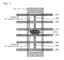
- FIG. 1 is a perspective view schematically showing the construction of a conventional plasma display panel.
- the conventional plasma display panel comprises a front panel and a rear panel.
- the front panel comprises a front glass substrate 10 and the rear panel comprises a rear glass substrate 20.
- the front panel and the rear panel are parallel to each other with a predetermined distance therebetween.
- the sustain electrode pair comprises the scan electrode 11 and the sustain electrode 12.
- the scan electrode 11 comprises a transparent electrode 11a formed of a transparent ITO material and a bus electrode 11b formed of a metal material.
- the sustain electrode 12 comprises a transparent electrode 12a formed of a transparent ITO material and a bus electrode 12b formed of a metal material.
- the scan electrode 11 receives a scan signal for scanning a panel and a sustain signal for sustaining a discharge.
- the sustain electrode 12 mainly receives a sustain signal.
- a dielectric layer 13a is formed on the sustain electrode pair 11, 12, and it functions to limit the discharge current and provides insulation between the electrode pairs.
- a protection layer 14 is formed on a top surface of the dielectric layer 13a and is formed of magnesium oxide (MgO) so as to facilitate a discharge condition.
- MgO magnesium oxide
- a dielectric layer 13b is formed on the address electrodes 22 and functions to provide insulation between the address electrodes 22.
- Barrier ribs 21 are formed on the dielectric layer 13b and partition discharge cells.
- R, G and B phosphor layer 23 are coated between the barrier ribs 21 and the barrier ribs 21 and radiate a visible ray for displaying images.
- the front glass substrate 10 and the rear glass substrate 20 are adhered together by a sealing material.
- An inert gas such as helium (He), neon (Ne) or xeon (Xe), is injected into the plasma display panel on which an exhaust process has been performed.
- the conventional plasma display panel has a high manufacturing cost since it comprises expensive transparent electrodes 11a, 12a.
- a fence type electrode structure consisting of only the bus electrodes 11b, 12b has been proposed.
- FIG. 2 is a plan view of a discharge cell having a fence type electrode structure of the conventional plasma display panel.
- a plurality of scan bus electrodes 210 and a plurality of sustain bus electrodes 220 are formed on upper and lower sides of a discharge cells instead of obviating expensive transparent electrodes.
- a scan connection electrode 230 connecting the plurality of scan bus electrodes 210 and a sustain connection electrode 240 connecting the plurality of sustain bus electrodes 220 are also formed in the cell.
- the scan bus electrodes 210 connected by the scan connection electrode 230 and the sustain bus electrodes 220 connected by the sustain connection electrode 240 are spaced apart from each other at a predetermined distance, forming a discharge gap 250.
- the aspect ratio is low and discharge diffusion is poor. Therefore, there are problems in that the brightness and discharge efficiency of the plasma display panel are low.
- a plasma display panel comprises discharge cells partitioned by barrier ribs, upper electrode part and lower electrode part formed adjacent to the boundary of the discharge cells and applied with a first driving pulse, first center electrode part located between the upper electrode part and the lower electrode part and applied with a second driving pulse, and second center electrode part located between the first center electrode part and the lower electrode part and applied with the second driving pulse.
- the upper electrode part and the lower electrode part may perform the function of scan electrodes.
- the first center electrode part and the second center electrode part may perform the function of sustain electrodes.
- the upper electrode part and the lower electrode part may perform the function of sustain electrodes.
- the first center electrode part and the second center electrode part may perform the function of scan electrodes.
- a width of the upper electrode part may be equal to or more than 30 ⁇ m to less than or equal to 60 ⁇ m, and a width of the lower electrode part may be equal to or more than 30 ⁇ m to less than or equal to 60 ⁇ m.
- the upper electrode part and the lower electrode part may comprise only bus electrodes.
- a width of the first center electrode part may be equal to or more than 30 ⁇ m to less than or equal to 60 ⁇ m, and a width of the second center electrode part is equal to or more than 30 ⁇ m to less than or equal to 60 ⁇ m.
- the first center electrode part and the second center electrode part may comprise only bus electrodes.
- Each of the upper electrode part and the lower electrode part may comprise a plurality of bus electrodes.
- Each of the first center electrode part and the second center electrode part may comprise only a plurality of bus electrodes.
- the first center electrode part and the second center electrode part may be separate from each other.
- a plasma display panel comprises discharge cells partitioned by barrier ribs, upper electrode part and lower electrode part formed adjacent to the boundary of the discharge cells and applied with a first driving pulse, wherein each of upper electrode part and lower electrode part comprises a first protruding electrode part having one or more protruding electrodes that protrude toward the boundary of the discharge cells, first center electrode part located between the upper electrode part and the lower electrode part and applied with a second driving pulse, the first center electrode part comprising a first protruding electrode part having one or more protruding electrodes that protrude toward the center of the discharge cells, and second center electrode part located between the first center electrode part and the lower electrode part and applied with the second driving pulse, the second center electrode part comprising second protruding electrode part having one or more protruding electrodes that protrude toward the center of the discharge cells.
- a width of each of the protruding electrodes comprised in the first protruding electrode part may be equal to or more than 100 ⁇ m to less than or equal to 250 ⁇ m.
- a width of each of one or more protruding electrodes comprised in the second protruding electrode part may be equal to or more than 100 ⁇ m to less than or equal to 250 ⁇ m.
- the second protruding electrode part of the first center electrode part and the second protruding electrode part of the second center electrode part may be separate from each other.
- a minimum distance between the protruding electrodes comprised in the second protruding electrode part of the first center electrode part and the protruding electrodes comprised in the second protruding electrode part of the second center electrode part may be equal to or more than 50 ⁇ m to less than or equal to 200 ⁇ m.
- Each of the upper electrode part, the lower electrode part, the first center electrode part and the second center electrode part may comprises only a bus electrode.
- Each of the first protruding electrode part may comprise a number n (where, n is an odd number greater than 3) of protruding electrodes.
- the length of a protruding electrode located at the center, of the number n of the protruding electrodes, may range from 100% to 200% of that of one of the remaining protruding electrodes.
- Each of the first protruding electrode part may comprise a number n (where, n is an odd number greater than 3) of protruding electrodes.
- the length of a protruding electrode located at the center, of the number n of the protruding electrodes, may be equal to or more than 100 ⁇ m to less than or equal to 250 ⁇ m.
- Each of the second protruding electrode part may comprise a number M (where, M is an odd number greater than 3) of protruding electrodes.
- the length of a protruding electrode located at the center, of the number M of the protruding electrodes, may lie in the range 100% to 200% of that of one of the remaining protruding electrodes.
- Each of the second protruding electrode part may comprise a number M (where, M is an odd number greater than 3) of protruding electrodes.
- the length of a protruding electrode located at the center, of the number M of the protruding electrodes, may be equal to or more than 100 ⁇ m to less than or equal to 250 ⁇ m.
- a plasma display apparatus comprises discharge cells partitioned by barrier ribs, a first driving part that applies a first driving pulse, a second driving part that applies a second driving pulse, upper electrode part and lower electrode part formed adjacent to the boundary of the discharge cells and applied with the first driving pulse, first center electrode part located between the upper electrode part and the lower electrode part and applied with the second driving pulse, and second center electrode part located between the first center electrode part and the lower electrode part and applied with the second driving pulse.
- the first driving part may control the upper electrode part and the lower electrode part to serve as scan electrodes.
- the second driving part may control the first center electrode part and the second center electrode part to serve as sustain electrodes.
- the first driving part may control the upper electrode part and the lower electrode part to serve as sustain electrodes.
- the second driving part may control the first center electrode part and the second center electrode part to serve as scan electrodes.
- the first center electrode part and the second center electrode part may be separate from each other.
- Each of the upper electrode part and the lower electrode part may comprise first protruding electrode part protruding toward the boundary of the discharge cells.
- the first protruding electrode part may comprise one or more protruding electrodes.
- Each of the first center electrode part and the second center electrode part may comprise second protruding electrode part protruding toward the center of the discharge cells.
- the second protruding electrode part may comprise one or more protruding electrodes.
- the second protruding electrode part comprised in the first center electrode part and the second protruding electrode part comprised in the second center electrode part may be separate from each other.
- FIG. 1 is a perspective view schematically showing the construction of a conventional plasma display panel
- FIG. 2 is a plan view of a discharge cell having a fence type electrode structure of the conventional plasma display panel
- FIG. 3 is a plan view of a plasma display panel according to an embodiment of the present invention.
- FIG. 4 is a plan view of a plasma display panel according to another embodiment of the present invention.
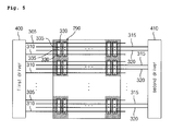
- FIG. 5 shows the construction of a plasma display apparatus according to the present invention.
- the plasma display panel according to the present invention comprises a discharge cell 290, an upper electrode part 305, a lower electrode part 310, a first center electrode part 315 and a second center electrode part 320.
- the discharge cell 290 is partitioned by a barrier rib 300 and provides a space in which a discharge is generated by an inert gas therein.
- the upper electrode part 305 and the lower electrode part 310 are formed adjacent to the boundary of the discharge cell 290, and are applied with a first driving pulse.
- the upper electrode part 305 and the lower electrode part 310 serve as one of scan electrodes and sustain electrodes. Therefore, if the upper electrode part 305 and the lower electrode part 310 serve as the scan electrodes, the first driving pulse can be a reset pulse, a scan pulse, a sustain pulse and the like, which are input to the scan electrodes. Meanwhile, if the upper electrode part 305 and the lower electrode part 310 serve as the sustain electrodes, the first driving pulse can be a sustain pulse, etc. which is input to the sustain electrodes.
- a width of each of the upper electrode part 305 or the lower electrode part 310 can be equal to or more than 30 ⁇ m to less than or equal to 60 ⁇ m.
- the upper electrode part 305 and the lower electrode part 310 comprise only the bus electrodes. It has been shown in FIG. 3 that the upper electrode part 305 and the lower electrode part 310 comprise only one bus electrode. However, the upper electrode part 305 and the lower electrode part 310 can comprise a plurality of bus electrodes.
- Each of the upper electrode part 305 and the lower electrode part 310 comprises a first protruding electrode part 330 that protrudes toward the boundary of an adjacent discharge cell.
- the first protruding electrode part 330 of each of the upper electrode part 305 and the lower electrode part 310 comprises one or more protruding electrodes.
- the first protruding electrode part 330 shown in FIG. 3 comprises one protruding electrode
- the first protruding electrode part 330 shown in FIG. 4 comprises a plurality of protruding electrodes.
- the first protruding electrode part 330 protruding from the upper electrode part 305 is protruded toward an upper boundary region direction of a discharge cell adjacent to the upper electrode part 305.
- the first protruding electrode part 330 protruding from the lower electrode part 310 is protruded toward a lower boundary region direction of a discharge cell adjacent to the lower electrode part 310.
- a width of the protruding electrodes comprised in the first protruding electrode part 330, respectively, can be equal to or more than 100 ⁇ m to less than or equal to 250 ⁇ m.
- the first protruding electrode part 330 can comprises an n number (where, n is an odd number greater than 3) of protruding electrodes.
- the length of a center protruding electrode located at the center of the n number of the protruding electrodes is 100% to 200% of that of one of the remaining peripheral protruding electrodes.
- the length of the center protruding electrode comprised in the first protruding electrode part 330 can be equal to or more than 100 ⁇ m to less than or equal to 250 ⁇ m.
- the first center electrode part 315 is located between the upper electrode part 305 and the lower electrode part 310, and is applied with a second driving pulse.
- the first center electrode part 315 forms a first discharge gap 370 corresponding to the upper electrode part 305. That is, if the upper electrode part 305 serves the scan electrode, the first center electrode part 315 receives the second driving pulse, such as a sustain pulse, in order to perform the function of the sustain electrode. Meanwhile, if the upper electrode part 305 serves as the sustain electrode, the first center electrode part 315 receives the second driving pulse such as a reset pulse, a scan pulse and a sustain pulse in order to perform the function of the scan electrode.
- a width of the first center electrode part 315 can be equal to or more than 30 ⁇ m to less than or equal to 60 ⁇ m.
- the second center electrode part 320 is located between the first center electrode part 315 and the lower electrode part 310, and is applied with the second driving pulse.
- the second center electrode part 320 forms a second discharge gap 380 corresponding to the lower electrode part 310. That is, if the lower electrode part 310 serves as the scan electrode, the second center electrode part 320 receives the second driving pulse, such as a sustain pulse, in order to perform the function of the sustain electrode. Meanwhile, if the lower electrode part 310 performs the function of the sustain electrode, the second center electrode part 320 receives the second driving pulse, such as a reset pulse, a scan pulse and a sustain pulse, in order to perform the function of the scan electrodes.
- a width of the second center electrode part 320 can be equal to or more than 30 ⁇ m to less than or equal to 60 ⁇ m.
- the first center electrode part 315 and the second center electrode part 320 consists only bus electrodes. It has been shown in FIG. 3 that each of the first center electrode part 315 and the second center electrode part 320 comprises only one bus electrode. However, each of the first center electrode part 315 and the second center electrode part 320 can comprise a plurality of bus electrodes.
- Each of the first center electrode part 315 and the second center electrode part 320 comprises a second protruding electrode part 335 that protrudes toward the center of the discharge cell 290.
- the second protruding electrode part 335 of each of the first center electrode part 315 and the second center electrode part 320 comprises one or more protruding electrodes.
- the second protruding electrode part 335 shown in FIG. 3 comprises one protruding electrode, and the second protruding electrode part 335 shown in FIG. 4 comprises a plurality of protruding electrodes.
- the second protruding electrode part 335 protruding from the first center electrode part 315 and the second protruding electrode part 335 protruding from the second center electrode part 320 are opposite to each other.
- a width of the protruding electrode comprised in the second protruding electrode part 335 can be equal to or more than 100 ⁇ m to less than or equal to 250 ⁇ m.
- the center protruding electrode of the second protruding electrode part 335 comprises an M number (where, M is an odd number greater than 3) of protruding electrodes.
- the length of a center protruding electrode located at the center of the M number of the protruding electrodes can range from 100% to 200% of that of one of the remaining peripheral protruding electrodes.
- the length of the center protruding electrode of the second protruding electrode part 335 can is equal to or more than 100 ⁇ m to less than or equal to 250 ⁇ m.
- Discharge diffusion by a plurality of protruding electrodes shown in FIG. 4 is smoothly performed compared with discharge diffusion by one protruding electrode shown in FIG. 3.
- the upper electrode part 305 and the lower electrode part 310 perform the function of the scan electrode
- the first center electrode part 315 and the second center electrode part 320 perform the function of the sustain electrode.
- the upper electrode part 305 and the lower electrode part 310 are applied with the sustain pulse, i.e., the first driving pulse at the same time.
- the first center electrode part 315 and the second center electrode part 320 are then applied with the sustain pulse, which alternates with the first driving pulse, at the same time.
- a sustain discharge is generated between the first discharge gap 370 formed between the upper electrode part 305 and the first center electrode part 315.
- a sustain discharge is generated in the second discharge gap 380 formed between the lower electrode part 310 and the second center electrode part 320.
- the present invention can increase brightness and discharge efficiency while accomplishing the aspect ratio by maximum.
- the sustain discharge generated in the first discharge gap 370 is diffused into the boundary direction of the discharge cell 290 by means of the first protruding electrode part 330 provided in the upper electrode part 305, and is also diffused into the center direction of the discharge cell 290 by means of the second protruding electrode part 335 provided in the first center electrode part 315.
- the sustain discharge generated in the second discharge gap 380 is diffused into the boundary direction of the discharge cell 290 by means of the first protruding electrode part 330 provided in the lower electrode part 310, and is also diffused into the center direction of the discharge cell 290 by means of the second protruding electrode part 335 provided in the second center electrode part 320.
- the sustain discharges generated in the first discharge gap 370 and the second discharge gap 380 are diffused into the entire region within the discharge cell 290. That is, in the fence type electrodes comprised in the conventional plasma display panel, since an area in which the electrodes and discharge spaces are overlapped with each other is small, discharge diffusion was poor. In electrodes comprised in the plasma display panel according to the present invention, however, the discharges generated in the two discharge gaps 370,380 are diffused into the entire region within the discharge cell 290. Therefore, the plasma display panel of the present invention can improve brightness and discharge efficiency.
- the area of the bus electrodes can be widened. Therefore, a sufficient amount of wall charges can be accumulated and discharge diffusion can be performed more smoothly. As a result, a discharge sustain voltage can be lowered and a strong discharge can be generated.
- the first center electrode part 315 and the second center electrode part 320 comprised in the plasma display panel constructed above according to the present invention can be preferably separated from each other.
- the wall charges move toward a surface of electrodes forming the other of the two discharge gaps due to the firstly generated discharge, and hinder a discharge that is generated in the other of the discharge gaps.
- the second protruding electrode part 335 comprised in the first center electrode part 315 and the second protruding electrode part 335 comprised in the second center electrode part 320 can be preferably spaced apart from each other.
- a minimum distance 360 between protruding electrodes comprised in the second protruding electrode part 335 of the first center electrode part 315 and protruding electrodes comprised in the second protruding electrode part 335 of the second center electrode part 320 is equal to or more than 50 ⁇ m to less than or equal to 200 ⁇ m.
- a plasma display apparatus comprises discharge cells 290, upper electrode part 305, lower electrode part 310, first center electrode part 315, second center electrode part 320, a first driving part 400 and a second driving part 410.
- the discharge cells 290 are partitioned by barrier ribs 300 and provide spaces in which a discharge is generated by an inert gas therein.
- the upper electrode part 305 and the lower electrode part 310 are formed adjacent to the boundary of the discharge cells 290 and are applied with a first driving pulse from the first driving part 400.
- a width of the upper electrode part 305 or the lower electrode part 310 can be preferably equal to or more than 30 ⁇ m to less than or equal to 60 ⁇ m.
- the upper electrode part 305 and the lower electrode part 310 constructed above comprise only bus electrodes.
- Each of the upper electrode part 305 and the lower electrode part 310 comprises a first protruding electrode part 330 that protrudes toward the boundary of adjacent discharge cells.
- the first protruding electrode part 330 of each of the upper electrode part 305 and the lower electrode part 310 comprises one or more protruding electrodes.
- the first protruding electrode part 330 can comprise one protruding electrode, as shown in FIG. 3, and can comprise a plurality of protruding electrodes, as shown in FIG. 4.
- the first protruding electrode part 330 protruding from the upper electrode part 305 protrude in an upper boundary region direction of a discharge cell adjacent to the upper electrode part 305.
- the first protruding electrode part 330 protruding from the lower electrode part 310 protrude in a lower boundary region direction of a discharge cell adjacent to the lower electrode part 310.
- a width of each of the protruding electrodes comprised in the first protruding electrode part 330 can be preferably equal to or more than 100 ⁇ m to less than or equal to 250 ⁇ m.
- the first center electrode part 315 is located between the upper electrode part 305 and the lower electrode part 310 and is applied with a second driving pulse from the second driving part 410.
- the first center electrode part 315 form the first discharge gap 370 corresponding to the upper electrode part 305.
- a width of the first center electrode part 315 can be preferably equal to or more than 30 ⁇ m to less than or equal to 60 ⁇ m.
- the second center electrode part 320 are located between the first center electrode part 315 and the lower electrode part 310 and are applied with the second driving pulse from the second driving part 410.
- the second center electrode part 320 forms the second discharge gap 380 corresponding to the lower electrode part 310.
- a width of the second center electrode part 320 can be preferably equal to or more than 30 ⁇ m to less than or equal to 60 ⁇ m.
- the first center electrode part 315 and the second center electrode part 320 comprised in the plasma display apparatus of the present invention can be preferably separated from each other.
- the second protruding electrode part 335 comprised in the first center electrode part 315 and the second protruding electrode part 335 comprised in the second center electrode part 320 can also be preferably separated from each other.
- the second protruding electrode part 335 comprises one or more protruding electrodes.
- the second protruding electrode part 335 can comprise one protruding electrode, as shown in FIG. 3, and the second protruding electrode part 335 can comprise a plurality of protruding electrodes, as shown in FIG. 4.
- a width of each of the protruding electrodes comprised in the second protruding electrode part 335 can be preferably equal to or more than 100 ⁇ m to less than or equal to 250 ⁇ m.
- the minimum distance 360 between the protruding electrodes comprised in the second protruding electrode part 335 of the first center electrode part 315 and the protruding electrodes comprised in the second protruding electrode part 335 of the second center electrode part 320 can be preferably equal to or more than 50 ⁇ m to less than or equal to 200 ⁇ m.
- the first driving part 400 applies the first driving pulse to the upper electrode part 305 and the lower electrode part 310.
- the second driving part 410 applies the second driving pulse to the first center electrode part 315 and the second center electrode part 320.
- the first driving part 400 applies the first driving pulse such as a reset pulse, a scan pulse or a sustain pulse to the upper electrode part 305 and the lower electrode part 310
- the second driving part 410 applies the second driving pulse, such as a sustain pulse, to the first center electrode part 315 and the second center electrode part 320. Therefore, the upper electrode part 305 and the lower electrode part 310 perform the function of the scan electrode and the first center electrode part 315 and the second center electrode part 320 perform the function of the sustain electrode.
- the first driving part 400 applies the first driving pulse, such as the sustain pulse, to the upper electrode part 305 and the lower electrode part 310
- the second driving part 410 applies the second driving pulse, such as the reset pulse, the scan pulse or the sustain pulse, to the first center electrode part 315 and the second center electrode part 320. Therefore, the upper electrode part 305 and the lower electrode part 310 perform the function of the sustain electrode and the first center electrode part 315 and the second center electrode part 320 perform the function of the scan electrode.
- the present invention since a plurality of discharge gaps and protruding electrodes are formed, the aspect ratio can be secured, a discharge amount can be increased and discharge diffusion can be smoothly performed. Therefore, the present invention is advantageous in that it can improve brightness and discharge efficiency since a discharge amount is increased and discharge diffusion is easily performed.
Landscapes
- Engineering & Computer Science (AREA)
- Physics & Mathematics (AREA)
- Plasma & Fusion (AREA)
- Chemical & Material Sciences (AREA)
- Materials Engineering (AREA)
- Gas-Filled Discharge Tubes (AREA)
Applications Claiming Priority (2)
| Application Number | Priority Date | Filing Date | Title |
|---|---|---|---|
| KR1020040081127A KR100658315B1 (ko) | 2004-10-11 | 2004-10-11 | 스캔 전극과 서스테인 전극을 포함하는 플라즈마디스플레이 패널 |
| KR1020040081128A KR100680771B1 (ko) | 2004-10-11 | 2004-10-11 | 스캔 전극과 서스테인 전극을 포함하는 플라즈마디스플레이 패널 |
Publications (2)
| Publication Number | Publication Date |
|---|---|
| EP1646065A2 true EP1646065A2 (fr) | 2006-04-12 |
| EP1646065A3 EP1646065A3 (fr) | 2009-05-06 |
Family
ID=36144566
Family Applications (1)
| Application Number | Title | Priority Date | Filing Date |
|---|---|---|---|
| EP05256304A Withdrawn EP1646065A3 (fr) | 2004-10-11 | 2005-10-11 | Panneau d'affichage à plasma et appareil d'affichage à plasma avec électrodes |
Country Status (3)
| Country | Link |
|---|---|
| US (1) | US20060076877A1 (fr) |
| EP (1) | EP1646065A3 (fr) |
| JP (1) | JP2006114496A (fr) |
Families Citing this family (4)
| Publication number | Priority date | Publication date | Assignee | Title |
|---|---|---|---|---|
| KR100762249B1 (ko) * | 2006-05-30 | 2007-10-01 | 엘지전자 주식회사 | 플라즈마 디스플레이 장치 |
| KR100811605B1 (ko) * | 2006-08-18 | 2008-03-11 | 엘지전자 주식회사 | 플라즈마 디스플레이 패널 |
| KR20080017204A (ko) * | 2006-08-21 | 2008-02-26 | 엘지전자 주식회사 | 플라즈마 디스플레이 패널 |
| WO2008136051A1 (fr) * | 2007-04-24 | 2008-11-13 | Hitachi, Ltd. | Ecran d'affichage à plasma |
Citations (5)
| Publication number | Priority date | Publication date | Assignee | Title |
|---|---|---|---|---|
| US20010011974A1 (en) * | 2000-02-03 | 2001-08-09 | Lg Electronics Inc. | Plasma display panel and driving method thereof |
| EP1146538A2 (fr) * | 2000-03-22 | 2001-10-17 | Fujitsu Hitachi Plasma Display Limited | Panneau d'affichage à plasma |
| US20020005822A1 (en) * | 1999-11-15 | 2002-01-17 | Lg Electronics, Inc. | Plasma display and driving method thereof |
| EP1187165A2 (fr) * | 2000-09-01 | 2002-03-13 | Fujitsu Hitachi Plasma Display Limited | Dispositif d'affichage à plasma |
| US20040113555A1 (en) * | 2002-12-12 | 2004-06-17 | Seong-Hoon Han | Plasma display panel without transparent electrode |
Family Cites Families (4)
| Publication number | Priority date | Publication date | Assignee | Title |
|---|---|---|---|---|
| US6630788B1 (en) * | 1999-05-14 | 2003-10-07 | Lg Electronics Inc. | Plasma display panel |
| CN1263068C (zh) * | 1999-06-04 | 2006-07-05 | 松下电器产业株式会社 | 等离子体显示面板 |
| JP2003007216A (ja) * | 2001-06-25 | 2003-01-10 | Nec Corp | プラズマディスプレイパネル及びその製造方法 |
| US20050093445A1 (en) * | 2003-11-05 | 2005-05-05 | Lg Electronics Inc. | Plasma display panel |
-
2005
- 2005-10-11 US US11/246,143 patent/US20060076877A1/en not_active Abandoned
- 2005-10-11 EP EP05256304A patent/EP1646065A3/fr not_active Withdrawn
- 2005-10-11 JP JP2005296101A patent/JP2006114496A/ja active Pending
Patent Citations (5)
| Publication number | Priority date | Publication date | Assignee | Title |
|---|---|---|---|---|
| US20020005822A1 (en) * | 1999-11-15 | 2002-01-17 | Lg Electronics, Inc. | Plasma display and driving method thereof |
| US20010011974A1 (en) * | 2000-02-03 | 2001-08-09 | Lg Electronics Inc. | Plasma display panel and driving method thereof |
| EP1146538A2 (fr) * | 2000-03-22 | 2001-10-17 | Fujitsu Hitachi Plasma Display Limited | Panneau d'affichage à plasma |
| EP1187165A2 (fr) * | 2000-09-01 | 2002-03-13 | Fujitsu Hitachi Plasma Display Limited | Dispositif d'affichage à plasma |
| US20040113555A1 (en) * | 2002-12-12 | 2004-06-17 | Seong-Hoon Han | Plasma display panel without transparent electrode |
Also Published As
| Publication number | Publication date |
|---|---|
| JP2006114496A (ja) | 2006-04-27 |
| US20060076877A1 (en) | 2006-04-13 |
| EP1646065A3 (fr) | 2009-05-06 |
Similar Documents
| Publication | Publication Date | Title |
|---|---|---|
| JP2000251745A (ja) | プラズマディスプレイパネル | |
| US6806645B2 (en) | Plasma display panel | |
| EP1592039A1 (fr) | Panneau d'affichage à plasma | |
| US7486022B2 (en) | Plasma display panel (PDP) | |
| EP1646065A2 (fr) | Panneau d'affichage à plasma et appareil d'affichage à plasma avec électrodes | |
| KR100366099B1 (ko) | 격벽의 폭이 다르게 형성된 플라즈마 디스플레이 패널 | |
| US7135819B2 (en) | Plasma display panel | |
| US20060097636A1 (en) | Plasma display panel | |
| KR20050013862A (ko) | 플라즈마 디스플레이 패널 | |
| JP2001135248A (ja) | プラズマディスプレーパネルの電極構造及び維持電極駆動方法 | |
| EP1717839A1 (fr) | Panneau d'affichage à plasma | |
| EP1646066A2 (fr) | Panneau d'affichage à plasma et appareil d'affichage à plasma ave électrodes | |
| KR100340444B1 (ko) | 고주파 플라즈마 디스플레이 패널 | |
| KR100615241B1 (ko) | 방전 전극의 구조가 개선된 플라즈마 디스플레이 패널 | |
| KR100613013B1 (ko) | 플라즈마 표시 패널 | |
| JP3729319B2 (ja) | プラズマディスプレイパネル、その駆動方法及びその駆動装置 | |
| KR100658315B1 (ko) | 스캔 전극과 서스테인 전극을 포함하는 플라즈마디스플레이 패널 | |
| EP1791153A2 (fr) | Ecran plasma | |
| EP1646064A2 (fr) | Ecran à plasma | |
| WO2004077486A1 (fr) | Ecran a plasma | |
| KR100626067B1 (ko) | 플라즈마 디스플레이 패널 | |
| KR100718996B1 (ko) | 전극을 포함하는 플라즈마 디스플레이 패널 | |
| KR100599605B1 (ko) | 플라즈마 디스플레이 패널 | |
| KR100680771B1 (ko) | 스캔 전극과 서스테인 전극을 포함하는 플라즈마디스플레이 패널 | |
| KR100730203B1 (ko) | 플라즈마 디스플레이 패널 |
Legal Events
| Date | Code | Title | Description |
|---|---|---|---|
| PUAI | Public reference made under article 153(3) epc to a published international application that has entered the european phase |
Free format text: ORIGINAL CODE: 0009012 |
|
| 17P | Request for examination filed |
Effective date: 20051108 |
|
| AK | Designated contracting states |
Kind code of ref document: A2 Designated state(s): AT BE BG CH CY CZ DE DK EE ES FI FR GB GR HU IE IS IT LI LT LU LV MC NL PL PT RO SE SI SK TR |
|
| AX | Request for extension of the european patent |
Extension state: AL BA HR MK YU |
|
| PUAL | Search report despatched |
Free format text: ORIGINAL CODE: 0009013 |
|
| AK | Designated contracting states |
Kind code of ref document: A3 Designated state(s): AT BE BG CH CY CZ DE DK EE ES FI FR GB GR HU IE IS IT LI LT LU LV MC NL PL PT RO SE SI SK TR |
|
| AX | Request for extension of the european patent |
Extension state: AL BA HR MK YU |
|
| RIC1 | Information provided on ipc code assigned before grant |
Ipc: H01J 17/04 20060101ALI20090331BHEP Ipc: H01J 17/49 20060101AFI20060206BHEP |
|
| STAA | Information on the status of an ep patent application or granted ep patent |
Free format text: STATUS: THE APPLICATION HAS BEEN WITHDRAWN |
|
| 18W | Application withdrawn |
Effective date: 20090709 |