EP1645899A2 - Optical apparatus and image-taking system - Google Patents
Optical apparatus and image-taking system Download PDFInfo
- Publication number
- EP1645899A2 EP1645899A2 EP05256256A EP05256256A EP1645899A2 EP 1645899 A2 EP1645899 A2 EP 1645899A2 EP 05256256 A EP05256256 A EP 05256256A EP 05256256 A EP05256256 A EP 05256256A EP 1645899 A2 EP1645899 A2 EP 1645899A2
- Authority
- EP
- European Patent Office
- Prior art keywords
- image
- optical
- light
- camera
- photoelectric conversion
- Prior art date
- Legal status (The legal status is an assumption and is not a legal conclusion. Google has not performed a legal analysis and makes no representation as to the accuracy of the status listed.)
- Granted
Links
- 230000003287 optical effect Effects 0.000 title claims abstract description 153
- 238000001514 detection method Methods 0.000 claims abstract description 32
- 210000001747 pupil Anatomy 0.000 claims abstract description 30
- 238000006243 chemical reaction Methods 0.000 claims abstract description 21
- 230000010287 polarization Effects 0.000 claims description 34
- 239000000463 material Substances 0.000 claims description 4
- 230000001419 dependent effect Effects 0.000 claims 1
- 239000004973 liquid crystal related substance Substances 0.000 description 23
- 239000000758 substrate Substances 0.000 description 17
- 239000011521 glass Substances 0.000 description 13
- 239000011347 resin Substances 0.000 description 12
- 229920005989 resin Polymers 0.000 description 12
- 238000000034 method Methods 0.000 description 7
- 229920000106 Liquid crystal polymer Polymers 0.000 description 3
- 239000004977 Liquid-crystal polymers (LCPs) Substances 0.000 description 3
- 230000004075 alteration Effects 0.000 description 3
- 238000003384 imaging method Methods 0.000 description 3
- 238000004519 manufacturing process Methods 0.000 description 2
- 230000011514 reflex Effects 0.000 description 2
- 238000000926 separation method Methods 0.000 description 2
- 239000004642 Polyimide Substances 0.000 description 1
- 238000003848 UV Light-Curing Methods 0.000 description 1
- 230000008033 biological extinction Effects 0.000 description 1
- 239000006185 dispersion Substances 0.000 description 1
- 238000010438 heat treatment Methods 0.000 description 1
- 230000001678 irradiating effect Effects 0.000 description 1
- 238000000465 moulding Methods 0.000 description 1
- 229920001721 polyimide Polymers 0.000 description 1
- 230000001737 promoting effect Effects 0.000 description 1
- 238000003530 single readout Methods 0.000 description 1
- 239000002904 solvent Substances 0.000 description 1
Images




Classifications
-
- G—PHYSICS
- G02—OPTICS
- G02B—OPTICAL ELEMENTS, SYSTEMS OR APPARATUS
- G02B7/00—Mountings, adjusting means, or light-tight connections, for optical elements
- G02B7/28—Systems for automatic generation of focusing signals
-
- G—PHYSICS
- G02—OPTICS
- G02B—OPTICAL ELEMENTS, SYSTEMS OR APPARATUS
- G02B5/00—Optical elements other than lenses
- G02B5/18—Diffraction gratings
- G02B5/1833—Diffraction gratings comprising birefringent materials
-
- G—PHYSICS
- G02—OPTICS
- G02B—OPTICAL ELEMENTS, SYSTEMS OR APPARATUS
- G02B5/00—Optical elements other than lenses
- G02B5/30—Polarising elements
- G02B5/3016—Polarising elements involving passive liquid crystal elements
-
- G—PHYSICS
- G02—OPTICS
- G02B—OPTICAL ELEMENTS, SYSTEMS OR APPARATUS
- G02B7/00—Mountings, adjusting means, or light-tight connections, for optical elements
- G02B7/28—Systems for automatic generation of focusing signals
- G02B7/34—Systems for automatic generation of focusing signals using different areas in a pupil plane
-
- G—PHYSICS
- G02—OPTICS
- G02B—OPTICAL ELEMENTS, SYSTEMS OR APPARATUS
- G02B7/00—Mountings, adjusting means, or light-tight connections, for optical elements
- G02B7/28—Systems for automatic generation of focusing signals
- G02B7/34—Systems for automatic generation of focusing signals using different areas in a pupil plane
- G02B7/343—Systems for automatic generation of focusing signals using different areas in a pupil plane using light beam separating prisms
-
- G—PHYSICS
- G02—OPTICS
- G02B—OPTICAL ELEMENTS, SYSTEMS OR APPARATUS
- G02B7/00—Mountings, adjusting means, or light-tight connections, for optical elements
- G02B7/28—Systems for automatic generation of focusing signals
- G02B7/36—Systems for automatic generation of focusing signals using image sharpness techniques, e.g. image processing techniques for generating autofocus signals
- G02B7/38—Systems for automatic generation of focusing signals using image sharpness techniques, e.g. image processing techniques for generating autofocus signals measured at different points on the optical axis, e.g. focussing on two or more planes and comparing image data
-
- G—PHYSICS
- G03—PHOTOGRAPHY; CINEMATOGRAPHY; ANALOGOUS TECHNIQUES USING WAVES OTHER THAN OPTICAL WAVES; ELECTROGRAPHY; HOLOGRAPHY
- G03B—APPARATUS OR ARRANGEMENTS FOR TAKING PHOTOGRAPHS OR FOR PROJECTING OR VIEWING THEM; APPARATUS OR ARRANGEMENTS EMPLOYING ANALOGOUS TECHNIQUES USING WAVES OTHER THAN OPTICAL WAVES; ACCESSORIES THEREFOR
- G03B13/00—Viewfinders; Focusing aids for cameras; Means for focusing for cameras; Autofocus systems for cameras
- G03B13/02—Viewfinders
- G03B13/06—Viewfinders with lenses with or without reflectors
-
- G—PHYSICS
- G03—PHOTOGRAPHY; CINEMATOGRAPHY; ANALOGOUS TECHNIQUES USING WAVES OTHER THAN OPTICAL WAVES; ELECTROGRAPHY; HOLOGRAPHY
- G03B—APPARATUS OR ARRANGEMENTS FOR TAKING PHOTOGRAPHS OR FOR PROJECTING OR VIEWING THEM; APPARATUS OR ARRANGEMENTS EMPLOYING ANALOGOUS TECHNIQUES USING WAVES OTHER THAN OPTICAL WAVES; ACCESSORIES THEREFOR
- G03B13/00—Viewfinders; Focusing aids for cameras; Means for focusing for cameras; Autofocus systems for cameras
- G03B13/32—Means for focusing
- G03B13/34—Power focusing
- G03B13/36—Autofocus systems
-
- G—PHYSICS
- G03—PHOTOGRAPHY; CINEMATOGRAPHY; ANALOGOUS TECHNIQUES USING WAVES OTHER THAN OPTICAL WAVES; ELECTROGRAPHY; HOLOGRAPHY
- G03B—APPARATUS OR ARRANGEMENTS FOR TAKING PHOTOGRAPHS OR FOR PROJECTING OR VIEWING THEM; APPARATUS OR ARRANGEMENTS EMPLOYING ANALOGOUS TECHNIQUES USING WAVES OTHER THAN OPTICAL WAVES; ACCESSORIES THEREFOR
- G03B19/00—Cameras
- G03B19/02—Still-picture cameras
- G03B19/12—Reflex cameras with single objective and a movable reflector or a partly-transmitting mirror
Definitions
- the present invention relates to an optical apparatus having an autofocus (“AF") control using a photoelectric conversion element (“PCE”).
- AF autofocus
- PCE photoelectric conversion element
- a single lens reflex type digital still camera or digital single lens reflex (“DSLR”) camera adopts the so-called pupil slicing focus detection for precise focusing upon a quickly moving subject.
- FIG. 7 shows a schematic structure of a conventional DSLR camera system.
- a photographer observes a subject through an eyepiece 104
- part of light 110 from the subject that transmits an image-taking lens 120 is reflected on a main mirror 101 and forms a subject image on a focusing glass 102 in a camera body 100.
- the subject image formed on the focusing glass 102 is guided to the photographer's eye via a penta prism 103 and the eyepiece 104.
- both the main mirror 101 and sub-mirror 105 retreat from the optical path and the light from the subject which has passed the image-taking lens 120 is guided to the image sensor 108.
- the pupil slicing focus detection method of a through the taking lens (“TTL”) phase difference detection (“PDD”) requires a sensor dedicated for a focus detection and a secondary imaging optical system, and thus has difficulties in reducing a size and cost of the camera.
- JP 9-43507 inserts, near a pupil of the image-taking lens, a mask that transmits the light from part of the pupil, and detects focus using a signal from the image sensor corresponding to two images by switching an opening position of the mask.
- Another focus detection system proposed in JP 2004-46132, uses part of the image sensor as an AF sensor area, and guides to the area two lights split by a split image prism provided in the imaging optical system.
- JP 4-147207 discloses another structure for the TTL PDD AF by arranging a holographic optical element closer to the object side.
- the focus detection method proposed in JP 9-43507 changes the mask opening position, reads twice an image of the light that passes different pupil areas in the image-taking lens as an output (image signal) of the image sensor, compares these image signals. It takes a relatively long time to switch the mask opening position and to read two image signals from the image sensor. This focus detection method is rather unsuitable for a quickly moving subject.
- a method that uses a split image prism proposed in JP 2004-46132 needs a larger image than the split image prism, different from the TTL PDD.
- this method determines that it is defocused even if it is focused. Therefore, this method has a limited focus detection capability or is inferior to the TTL PDD.
- a method that uses the holographic optical element proposed in JP 4-147207 is similar to the TTL PDD in principle, but the holographic optical element possesses large color dispersion that causes an image to contain aberration in forming two AF images in the pupil slicing direction, which are important to a determination of the focusing state. Thus, this method is not practicable for the focus detection.
- An embodiment of the present invention seeks to provide an optical apparatus that provides quick and precise TTL PDD and pupil slicing focus detection.
- An optical apparatus includes a first optical element for splitting a first polarized light component contained in light that passes an exit pupil of a first optical system and directs to a photoelectric conversion element so that the first polarized light component direct to different light-receiving areas on the photoelectric conversion element.
- the optical apparatus may further include a second optical element for separating a second polarized light component contained in the light from said first optical element, from the first polarized light component.
- An image-taking system includes a lens unit that includes a first optical system, and the above optical apparatus that serves as an image-taking apparatus, onto which said lens unit is mounted.
- FIG. 1 shows a schematic structure of a DSLR camera system according to an embodiment of the present invention. Those elements in FIG. 1, which are the corresponding elements in FIG. 7, are designated by the same reference numerals.
- the image-taking lens 120 includes an image-taking optical system 125, and a lens controller, such as a MPU (not shown) etc.
- the image-taking optical system 125 serves as a first optical system that includes plural lenses including a focus lens 123 and a stop 124.
- the lens controller can communicate with a camera controller 309, such as an MPU, provided in the camera body 300, via a lens-side contact 122 and a camera-side contact 112.
- the camera controller 309 has an image processing function that generates a subject image based on a signal from an image-pickup device 108, which will be described later, and a focus detection function that detects a focusing state of the imaging-taking optical system 125 based on the signal from the image-pickup device 108, and operates a driving amount of the focus lens 123.
- 200 denotes an optical deflector element that serves as a first optical element, and its concrete structure will be described later.
- 108 denotes an image-pickup device (or an image sensor) that serves as a PCE, such as a CCD sensor and a CMOS sensor.
- a polarization beam splitter (“PBS") 301 that serves as a second optical element is provided between the optical deflector element 200 and the image-pickup device 108.
- An infrared extinction and low-pass filter 107 is provided just prior to the image-taking element 108.
- 102 denotes a focusing glass.
- 103 denotes a penta prism that introduces a subject image formed on the focusing glass 102 to the eyepiece 104.
- the focusing glass 102, the penta prism 103 and the eyepiece 104 form a finder optical system that serves as a second optical system.
- FIG. 2 denotes an optical path in detecting the focusing state of the image-taking optical system 125 or at the focus detection time in the above camera system.
- the light 110 from the subject passes the image-taking optical system 125, and is incident upon the optical deflector element 200.
- This light 110 is a non-polarized light.
- the optical deflector element 200 deflects and transmits, in the +y direction part, (referred to as "plus deflected light” hereinafter) 211 of a first polarized light component that has a polarization plane parallel to the zx plane among the light 110.
- the PBS 301 serves to transmit the first polarized light component and reflect a second polarized light component having a polarization plane orthogonal to the zx plane (or parallel to the yz plane).
- the plus deflected light 211 of the first polarized light component passes through the PBS 301, and condenses in an upper light-receiving area of the image-pickup device 108 in FIG. 2.
- Part (referred to as "minus deflected light” hereinafter) 212 of the first polarized light component is deflected in the -y direction, passes through the PBS 301, and condenses in a lower light-receiving area of the image-pickup device 108 in FIG. 2.
- the plus and minus deflected lights 211 and 212 among the first polarized light component which have reached the image-pickup device 108 are lights that have passed different areas of the exit pupil of the image-taking optical system 125. Therefore, the plus and minus deflected lights 211 and 212 form a pair of images on the image-pickup device 108, providing the pupil slicing focus detection based on the output or image signals from the image-pickup device 108 corresponding to the pair.
- the second polarized light component 210 contained in the light 110 travels straight and passes the optical deflector element 200, is reflected on the PBS 301 as the second optical element, and condenses on the focusing glass 102, forming the subject image.
- the first polarized light component including the plus and minus deflected lights 211 and 212
- a photographer can observe the subject image via the finder optical system.
- the optical deflector element 200 includes in order from a light incident side, as shown in FIG. 3D, a resin substrate 201 having a blazed diffraction grating, liquid crystal 202 filled in the grooves or concaves of the diffraction grating, a polarization film 204 having a pair of openings 204a and 204b as shown in FIG. 3C, and a glass substrate 203 adhered to the polarization film 204.
- the resin substrate 201 includes, as shown in FIG. 3A, first and second diffraction gratings 201a and 201b having different blazed directions from each other, and these blazed diffraction gratings 201a and 201b are manufactured by a molding method that uses the resin substrate 201 and a mold.
- the uniaxial light-transmitting liquid crystal 202 is filled, as shown in FIG. 3B, in the grating grooves of each of both the diffraction gratings 201a and 201b in the resin substrate 201.
- the material of the liquid crystal 202 is selected so that the ordinary index "no" of the liquid crystal 202 is approximately equal to the refractive index "ng" of the resin substrate 201.
- the diffraction gratings 201a and 201b are oriented by applying an orientation film made of polyimide, etc. onto the surfaces of the diffraction gratings 201a and 201b.
- the liquid crystal 202 is cured by irradiating the ultraviolet ("UV") light, after the solvent is vaporized by filling and heating the UV curing liquid crystal 202 in the grating grooves.
- the molecular axis of the liquid crystal polymer orientates approximately parallel to the grating groove direction (or x direction) of each of the diffraction gratings 201a and 201b.
- FIG. 3B shows a molecular axis of the liquid crystal polymer in a stick shape. The molecular axis direction of the liquid crystal polymer approximately accords with the optical-axis direction relative to the polarized light.
- the glass substrate 203 pasted with the polarization film 204 is adhered to the side of the liquid crystal 202 of the resin substrate 201 in which the liquid crystal 202 is filled and cured in the grating grooves.
- the openings 204a and 204b in the polarization film 204 are arranged in areas corresponding to the diffraction gratings 201a and 201b.
- the openings 204a and 204b are arranged symmetrical with respect to the yz plane including the optical axis (or z axis).
- the polarization film 204 is arranged so that its polarization or optical axis is approximately orthogonal to the optical-axis direction of the liquid crystal 202 filled in the grating grooves.
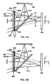
- FIGs. 4A and 4B show a separation of the second polarized light component 210 used for the finder observation from the first polarized light component (plus deflected light 211 and minus deflected light 212) used for the focus detection.
- FIG. 4A shows an optical path of a plane orthogonal to the zx plane that passes the center of the opening 204a in the polarization film 204 provided in the optical deflector element 200.
- the opening 204a in the polarization film 204 transmits a part (or first area) of the exit pupil in the image-taking optical system 125, and receives the light that has passed the diffraction grating 201a, i . e ., the first and second polarized light components.
- the polarization axis direction of the polarization film 204 is set so that it absorbs the first polarized light component having the polarization plane parallel to the zx plane.
- the molecular axis of the liquid crystal 202 filled in the grating grooves in the diffraction grating 201a orientates approximately parallel to the grating groove direction or the x direction.
- An extraordinary index "ne" of the liquid crystal 202 and the refractive index "ng" of the resin substrate 201 have the following relationship: n e > n g
- the first polarized light component having the polarization plane approximately parallel to the molecular axis of the liquid crystal 202 is deflected in the + y direction as illustrated.
- Part of the first polarized light component that has transmitted the liquid crystal 202 is absorbed in the polarization film 204, but the plus deflected light 211 of the first polarized light component that has passed the opening 204a in the polarization film 204 and the glass substrate 203 transmits the PBS 301 and reaches the upper light-receiving area in the image-pickup device 108 as illustrated.
- the resin substrate 201 has a refractive index ng of 1.5
- the liquid crystal 202 has an extraordinary index ne of 1.7
- a necessary deflecting angle ⁇ is 8°for the plus deflected light 211
- a desired deflecting angle ⁇ is obtained by setting the grating pitch p of each of the diffraction gratings 201a and 201b to 4 ⁇ m, and an inclination angle ⁇ of the resin substrate 201 to 35°.
- FIG. 4B shows an optical path of a plane orthogonal to the zx plane that passes the center of the opening 204b in the polarization film 204 provided in the optical deflector element 200.
- the opening 204b in the polarization film 204 receives the light that has passed another part (or second area) of the exit pupil in the image-taking optical system 125, i . e ., the first and second polarized light components.
- the molecular axis of the liquid crystal 202 filled in the grating grooves in the diffraction grating 201b orientates approximately parallel to the grating groove direction or the x direction, and the refractive index ng of the resin substrate 201 and the extraordinary index ne of the liquid crystal 202 have the above relationship defined in Equation (1). Therefore, the first polarized light component having the polarization plane (parallel to the zx plane) approximately parallel to the molecular axis of the liquid crystal 202 is deflected in the -y direction in FIG. 4A.
- Part of the first polarized light that transmits the liquid crystal 202 is absorbed in the polarized film 204, but the minus deflected light 212 of the first polarized light component that has passed the opening 204b in the polarization film 204 and the glass substrate 203 transmits the PBS 301 and reaches the lower light-receiving area in the image-pickup device 108 as illustrated.
- the ordinary index "no" of the liquid crystal 202 and the refractive index "ng" of the resin substrate 201 have the following relationship: n o ⁇ n g Therefore, the second polarized light component 210 having the polarization plane (parallel to the yz plane) orthogonal to the molecular axis of the liquid crystal 202 travels straight without being subject to the deflections by the diffraction gratings 201a and 201b.
- the first polarized light component 210 is reflected by the PBS 301, condenses on the focusing glass 102, and forms the subject image. A photographer observes the subject image formed on the focusing glass 102 via the penta prism 103 and the eyepiece 104.
- FIG. 5A shows an optical path when the image-taking optical system 125 is focused on a predetermined subject.
- the plus and minus deflected lights 211 and 212 that have passed the openings 204a and 204b in the polarization film 204 transmit the PBS 301, which is omitted in FIG. 5A, and image on the image-pickup device 108.
- FIG. 5D shows image signals from predetermined two lines extending in the x direction in the image-pickup device 108, which correspond to two images formed by the plus and minus deflected lights 211 and 212.
- an image (signal) A formed by the plus deflected light 211 that passes the opening 204a accords in the x direction on the image-pickup device 108 with an image (signal) B formed by the minus deflected light 212 that passes the opening 204b, because the image-taking optical system 125 is focused on the subject.
- FIG. 5B shows an optical path when the image-taking optical system 125 is in the front focus state to the subject or focused on a position before the subject.
- the plus and minus deflected lights 211 and 212 once image before the image-pickup device 108, diverge, and reach the image-pickup device 108.
- FIG. 5E shows an image signal from the above two lines corresponding to two images formed by the plus and minus deflected lights 211 and 212.
- the image-taking optical system 125 Since the image-taking optical system 125 is in the front focus state, the image (signal) A formed by the plus deflected light 211 that passes the opening 204a shifts from in the -x direction on the image-pickup device 108 with the image (signal) B formed by the minus deflected light 212 that passes the opening 204b.
- the camera controller 309 shown in FIG. 1 detects a defocus amount and a defocus direction (or front focus direction) of the image-taking optical system 125 based on the shifting direction and a positional relationship (or phase difference) between the images A and B.
- FIG. 5C shows an optical path when the image-taking optical system 125 is in the so-called back focus state to the subject or focused on a position after the subject.
- the plus and minus deflected lights 211 and 212 divergently enter the image-pickup device 108.
- FIG. 5F shows an image signal from the above two lines corresponding to two images formed by the plus and minus deflected lights 211 and 212.
- the image-taking optical system 125 Since the image-taking optical system 125 is in the back focus state, the image (signal) A formed by the plus deflected light 211 that passes the opening 204a shifts from in the +x direction on the image-pickup device 108 with the image (signal) B formed by the minus deflected light 212 that passes the opening 204b.
- the camera controller 309 shown in FIG. 1 detects a defocus amount and a defocus direction (or front focus direction) of the image-taking optical system 125 based on the shifting direction and a positional relationship (or phase difference) between the images A and B.
- the camera controller 309 Based on the detected defocus direction and defocus amount, the camera controller 309 operates a driving direction and a driving amount necessary for focusing of the focus lens 123 shown in FIG. 1, and controls driving of the focus lens 123 via the lens controller (not shown).
- the optical deflector element 200 of this embodiment that has a polarization characteristic is affected by the subject when the subject has a polarization characteristic, the optical deflector element 200 is affected.
- the optical deflector element 200 and the PBS 301 are retreated from the optical path between the image-taking optical system 125 and the image-pickup device 108 in photographing the subject with the image-pickup device 108.
- this embodiment detects focus using the image-pickup device while confirming the subject through the finder optical system, and dispenses with the sensor and optical system dedicated for detecting the focus, promoting the miniaturization and cost reduction of the camera.
- this embodiment can provide pupil slicing and TTL PDD focus detection based on the image formed by each defected light.
- the optical deflector element is configured to split and deflect the first polarized light component to form the focus detection images while transmitting the second polarized light component.
- the second polarized light component forms a non-distorted finder image.
- the second polarized light component that transmits the optical deflector element, is reflected on the PBS, and forms the finder image prevents drop of the light intensity of the finder image.
- the configuration that allows the PBS and the optical deflector element to retreat from the optical path between the image-taking optical system and the image-pickup device eliminates from a shot subject image distortion or lowed light intensity caused by the PBS and optical deflector element.
- the optical deflector element includes the first and second blazed diffraction gratings having different blaze directions, uniaxial light-transmitting material member, and polarization film, and provides an inexpensive optical element used for the pupil slicing focus detection.
- the optical deflector element 200 may be provided at or near the pupil position (a position of the stop 124) in the image-taking or interchangeable lens 420 as shown in FIG. 6.
- first and second embodiments discuss an interchangeable lens SLR camera system
- the present invention is applicable to other camera systems, such as an integrated lens camera system.
- the present invention may deflect only one of parts and introduce the other to the image-pickup device 108 without deflecting the other.
- a pair of images are formed, for example, at the top and center of the image-pickup device.
- a deflecting direction of each deflected light is not limited to these embodiments.
- the number of deflected lights and deflecting directions may increase so as to form four or more images.
- the optical deflector element 200 having a pair of blazed diffraction gratings
- another element that serves to deflect the light and generate less aberration may form the optical deflector element, in addition to the blazed diffraction grating.
- the optical deflector element that includes the liquid crystal filled in the grating grooves in the diffraction grating
- the arrangement between the diffraction grating and the liquid crystal is not limited to these embodiments.
- a member that encloses the liquid crystal between glass substrates may be arranged adjacent to the diffraction grating (or resin substrate).
- the first optical element may use an optical deflector element that splits part of the incident light by using an optical characteristic, such as a wavelength characteristic, other than the polarization characteristic.
- the above embodiments split the first polarized light component incident upon the first optical element, and form a pair of images on the PCE, more quickly providing an image signal than switching the mask opening position.
- a pair of images have less aberration suitable for the focus detection than the split image prism and the holographic optical element.
- TTL PDD and pupil slicing focus detection is available.
- a separation of a second light component, such as the second polarized light component, contained in the light from a first optical element, from a first light component, such as the first polarized light component, directing to the PCE, only a pair of images can be formed on the PCE while the second light component can be used for other applications, such as a finder observation.
Landscapes
- Physics & Mathematics (AREA)
- General Physics & Mathematics (AREA)
- Optics & Photonics (AREA)
- Chemical & Material Sciences (AREA)
- Crystallography & Structural Chemistry (AREA)
- Engineering & Computer Science (AREA)
- Computer Vision & Pattern Recognition (AREA)
- Focusing (AREA)
- Automatic Focus Adjustment (AREA)
- Studio Devices (AREA)
- Viewfinders (AREA)
- Transforming Light Signals Into Electric Signals (AREA)
Abstract
Description
- The present invention relates to an optical apparatus having an autofocus ("AF") control using a photoelectric conversion element ("PCE").
- A single lens reflex type digital still camera or digital single lens reflex ("DSLR") camera adopts the so-called pupil slicing focus detection for precise focusing upon a quickly moving subject.
- FIG. 7 shows a schematic structure of a conventional DSLR camera system. When a photographer observes a subject through an
eyepiece 104, part oflight 110 from the subject that transmits an image-takinglens 120 is reflected on amain mirror 101 and forms a subject image on a focusingglass 102 in acamera body 100. The subject image formed on the focusingglass 102 is guided to the photographer's eye via apenta prism 103 and theeyepiece 104. - Part of the
light 110 from the subject passes through themain mirror 101, and is reflected on asub-mirror 105 and guided to afocus detection unit 106. Thefocus detection unit 106 includes a field lens, a mirror, a stop mask, a secondary imaging lens, and a light-receiving sensor. The light-receiving sensor receives the light that passes different pupil areas on the image-taking lens 120, and an image signal is output from each of a pair of or plural pairs of line sensors in the light-receiving sensor. A focusing state (such as a defocus direction and a defocus amount) of the image-taking lens 120 can be detected based on a phase difference of this image signal. In addition, a driving direction and driving amount of afocus lens 123 in the image-taking lens 120 are calculated from the detected focusing state, and focus is obtained by driving thefocus lens 123. - In the image-taking time, both the
main mirror 101 andsub-mirror 105 retreat from the optical path and the light from the subject which has passed the image-taking lens 120 is guided to theimage sensor 108. - The pupil slicing focus detection method of a through the taking lens ("TTL") phase difference detection ("PDD") requires a sensor dedicated for a focus detection and a secondary imaging optical system, and thus has difficulties in reducing a size and cost of the camera.
- Accordingly, a digital still camera has recently been proposed which utilizes a subject taking image sensor for the TTL PDD and pupil slicing focus detection. For example, Japanese Patent Application, Publication No. ("JP") 9-43507 inserts, near a pupil of the image-taking lens, a mask that transmits the light from part of the pupil, and detects focus using a signal from the image sensor corresponding to two images by switching an opening position of the mask. Another focus detection system, proposed in JP 2004-46132, uses part of the image sensor as an AF sensor area, and guides to the area two lights split by a split image prism provided in the imaging optical system.
- JP 4-147207 discloses another structure for the TTL PDD AF by arranging a holographic optical element closer to the object side.
- However, the focus detection method proposed in JP 9-43507 changes the mask opening position, reads twice an image of the light that passes different pupil areas in the image-taking lens as an output (image signal) of the image sensor, compares these image signals. It takes a relatively long time to switch the mask opening position and to read two image signals from the image sensor. This focus detection method is rather unsuitable for a quickly moving subject.
- A method that uses a split image prism proposed in JP 2004-46132 needs a larger image than the split image prism, different from the TTL PDD. In addition, unless an image on the boundary of the split image prism has a linear shape, this method determines that it is defocused even if it is focused. Therefore, this method has a limited focus detection capability or is inferior to the TTL PDD.
- A method that uses the holographic optical element proposed in JP 4-147207 is similar to the TTL PDD in principle, but the holographic optical element possesses large color dispersion that causes an image to contain aberration in forming two AF images in the pupil slicing direction, which are important to a determination of the focusing state. Thus, this method is not practicable for the focus detection.
- An embodiment of the present invention seeks to provide an optical apparatus that provides quick and precise TTL PDD and pupil slicing focus detection.
- An optical apparatus according to one aspect of the present invention includes a first optical element for splitting a first polarized light component contained in light that passes an exit pupil of a first optical system and directs to a photoelectric conversion element so that the first polarized light component direct to different light-receiving areas on the photoelectric conversion element. The optical apparatus may further include a second optical element for separating a second polarized light component contained in the light from said first optical element, from the first polarized light component.
- An image-taking system according to another aspect of the present invention includes a lens unit that includes a first optical system, and the above optical apparatus that serves as an image-taking apparatus, onto which said lens unit is mounted.
- Optional features of the present invention will become readily apparent from the following description of the preferred embodiments with reference to the accompanying drawings.
- FIG. 1 is a schematic view of a structure of a camera system according to a first embodiment of the present invention.
- FIG. 2 is a schematic view of an optical path according to the first embodiment.
- FIGs. 3A to 3D are views for explaining a structure and manufacturing method of an optical deflector element according to the first embodiment.
- FIGs. 4A and 4B are schematic views of optical paths for a focus detection and for finder observation according to the first embodiment.
- FIG. 5 is an explanatory view showing a focus detection principle according to the first embodiment.
- FIG. 6 is a schematic view of a structure of a camera system according to a second embodiment of the present invention.
- FIG. 7 is a schematic view of a structure of a conventional camera system.
- Referring now to the accompanying drawings, a description will be given of a preferred embodiment of the present invention.
- FIG. 1 shows a schematic structure of a DSLR camera system according to an embodiment of the present invention. Those elements in FIG. 1, which are the corresponding elements in FIG. 7, are designated by the same reference numerals.
- 300 denotes a camera body (optical apparatus), onto which an image-taking or
interchangeable lens 120 is mounted via alens mount 121. - The image-
taking lens 120 includes an image-takingoptical system 125, and a lens controller, such as a MPU (not shown) etc. The image-takingoptical system 125 serves as a first optical system that includes plural lenses including afocus lens 123 and astop 124. The lens controller can communicate with acamera controller 309, such as an MPU, provided in thecamera body 300, via a lens-side contact 122 and a camera-side contact 112. Thecamera controller 309 has an image processing function that generates a subject image based on a signal from an image-pickup device 108, which will be described later, and a focus detection function that detects a focusing state of the imaging-takingoptical system 125 based on the signal from the image-pickup device 108, and operates a driving amount of thefocus lens 123. - In the
camera body optical deflector element 200 and the image-pickup device 108. An infrared extinction and low-pass filter 107 is provided just prior to the image-taking element 108. - 102 denotes a focusing glass. 103 denotes a penta prism that introduces a subject image formed on the focusing
glass 102 to theeyepiece 104. The focusingglass 102, thepenta prism 103 and theeyepiece 104 form a finder optical system that serves as a second optical system. - FIG. 2 denotes an optical path in detecting the focusing state of the image-taking
optical system 125 or at the focus detection time in the above camera system. - The
light 110 from the subject passes the image-takingoptical system 125, and is incident upon theoptical deflector element 200. Thislight 110 is a non-polarized light. Theoptical deflector element 200 deflects and transmits, in the +y direction part, (referred to as "plus deflected light" hereinafter) 211 of a first polarized light component that has a polarization plane parallel to the zx plane among thelight 110. The PBS 301 serves to transmit the first polarized light component and reflect a second polarized light component having a polarization plane orthogonal to the zx plane (or parallel to the yz plane). - Consequently, the plus
deflected light 211 of the first polarized light component passes through thePBS 301, and condenses in an upper light-receiving area of the image-pickup device 108 in FIG. 2. Part (referred to as "minus deflected light" hereinafter) 212 of the first polarized light component is deflected in the -y direction, passes through thePBS 301, and condenses in a lower light-receiving area of the image-pickup device 108 in FIG. 2. - The plus and minus
deflected lights pickup device 108 are lights that have passed different areas of the exit pupil of the image-takingoptical system 125. Therefore, the plus and minusdeflected lights pickup device 108, providing the pupil slicing focus detection based on the output or image signals from the image-pickup device 108 corresponding to the pair. - On the other hand, the second polarized
light component 210 contained in thelight 110 travels straight and passes theoptical deflector element 200, is reflected on thePBS 301 as the second optical element, and condenses on the focusingglass 102, forming the subject image. Thereby, even in detecting focus using the first polarized light component including the plus and minus deflectedlights - Referring now to FIGs. 3A to 3D, a description will be given of a structure and manufacture method of the
optical deflector element 200. Theoptical deflector element 200 includes in order from a light incident side, as shown in FIG. 3D, aresin substrate 201 having a blazed diffraction grating,liquid crystal 202 filled in the grooves or concaves of the diffraction grating, apolarization film 204 having a pair ofopenings glass substrate 203 adhered to thepolarization film 204. - The
resin substrate 201 includes, as shown in FIG. 3A, first andsecond diffraction gratings diffraction gratings resin substrate 201 and a mold. - The uniaxial light-transmitting
liquid crystal 202 is filled, as shown in FIG. 3B, in the grating grooves of each of both thediffraction gratings resin substrate 201. The material of theliquid crystal 202 is selected so that the ordinary index "no" of theliquid crystal 202 is approximately equal to the refractive index "ng" of theresin substrate 201. - The
diffraction gratings diffraction gratings liquid crystal 202 is cured by irradiating the ultraviolet ("UV") light, after the solvent is vaporized by filling and heating the UV curingliquid crystal 202 in the grating grooves. The molecular axis of the liquid crystal polymer orientates approximately parallel to the grating groove direction (or x direction) of each of thediffraction gratings - The
glass substrate 203 pasted with thepolarization film 204 is adhered to the side of theliquid crystal 202 of theresin substrate 201 in which theliquid crystal 202 is filled and cured in the grating grooves. Theopenings polarization film 204 are arranged in areas corresponding to thediffraction gratings openings polarization film 204 is arranged so that its polarization or optical axis is approximately orthogonal to the optical-axis direction of theliquid crystal 202 filled in the grating grooves. - Referring now to FIGs. 4A and 4B, a description will be given of the pupil slicing focus detection while the finder optical system observes the subject image.
- FIGs. 4A and 4B show a separation of the second
polarized light component 210 used for the finder observation from the first polarized light component (plus deflected light 211 and minus deflected light 212) used for the focus detection. - FIG. 4A shows an optical path of a plane orthogonal to the zx plane that passes the center of the
opening 204a in thepolarization film 204 provided in theoptical deflector element 200. Theopening 204a in thepolarization film 204 transmits a part (or first area) of the exit pupil in the image-takingoptical system 125, and receives the light that has passed thediffraction grating 201a, i.e., the first and second polarized light components. The polarization axis direction of thepolarization film 204 is set so that it absorbs the first polarized light component having the polarization plane parallel to the zx plane. - The molecular axis of the
liquid crystal 202 filled in the grating grooves in thediffraction grating 201a orientates approximately parallel to the grating groove direction or the x direction. An extraordinary index "ne" of theliquid crystal 202 and the refractive index "ng" of theresin substrate 201 have the following relationship:
liquid crystal 202 is deflected in the + y direction as illustrated. Part of the first polarized light component that has transmitted theliquid crystal 202 is absorbed in thepolarization film 204, but the plus deflected light 211 of the first polarized light component that has passed theopening 204a in thepolarization film 204 and theglass substrate 203 transmits thePBS 301 and reaches the upper light-receiving area in the image-pickup device 108 as illustrated. - For example, when the
resin substrate 201 has a refractive index ng of 1.5, theliquid crystal 202 has an extraordinary index ne of 1.7, and a necessary deflecting angle Φ is 8°for the plus deflected light 211, a desired deflecting angle Φ is obtained by setting the grating pitch p of each of thediffraction gratings resin substrate 201 to 35°. - FIG. 4B shows an optical path of a plane orthogonal to the zx plane that passes the center of the
opening 204b in thepolarization film 204 provided in theoptical deflector element 200. Theopening 204b in thepolarization film 204 receives the light that has passed another part (or second area) of the exit pupil in the image-takingoptical system 125, i.e., the first and second polarized light components. - The molecular axis of the
liquid crystal 202 filled in the grating grooves in thediffraction grating 201b orientates approximately parallel to the grating groove direction or the x direction, and the refractive index ng of theresin substrate 201 and the extraordinary index ne of theliquid crystal 202 have the above relationship defined in Equation (1). Therefore, the first polarized light component having the polarization plane (parallel to the zx plane) approximately parallel to the molecular axis of theliquid crystal 202 is deflected in the -y direction in FIG. 4A. Part of the first polarized light that transmits theliquid crystal 202 is absorbed in thepolarized film 204, but the minus deflectedlight 212 of the first polarized light component that has passed theopening 204b in thepolarization film 204 and theglass substrate 203 transmits thePBS 301 and reaches the lower light-receiving area in the image-pickup device 108 as illustrated. - The ordinary index "no" of the
liquid crystal 202 and the refractive index "ng" of theresin substrate 201 have the following relationship:
polarized light component 210 having the polarization plane (parallel to the yz plane) orthogonal to the molecular axis of theliquid crystal 202 travels straight without being subject to the deflections by thediffraction gratings polarized light component 210 is reflected by thePBS 301, condenses on the focusingglass 102, and forms the subject image. A photographer observes the subject image formed on the focusingglass 102 via thepenta prism 103 and theeyepiece 104. - Referring now to FIGs. 5A and 5B, a description will be given of a focus detection principle using the plus and minus deflected
lights optical system 125 is focused on a predetermined subject. Among the first polarized light component having a polarization plane parallel to the zx plane in FIG. 5A out of the light that passes the image-takingoptical system 125 and enters theoptical deflector element 200, the plus and minus deflectedlights openings polarization film 204 transmit thePBS 301, which is omitted in FIG. 5A, and image on the image-pickup device 108. FIG. 5D shows image signals from predetermined two lines extending in the x direction in the image-pickup device 108, which correspond to two images formed by the plus and minus deflectedlights - Although the plus and minus deflected
lights optical system 125, an image (signal) A formed by the plus deflected light 211 that passes theopening 204a accords in the x direction on the image-pickup device 108 with an image (signal) B formed by the minus deflected light 212 that passes theopening 204b, because the image-takingoptical system 125 is focused on the subject. - FIG. 5B shows an optical path when the image-taking
optical system 125 is in the front focus state to the subject or focused on a position before the subject. The plus and minus deflectedlights pickup device 108, diverge, and reach the image-pickup device 108. FIG. 5E shows an image signal from the above two lines corresponding to two images formed by the plus and minus deflectedlights - Since the image-taking
optical system 125 is in the front focus state, the image (signal) A formed by the plus deflected light 211 that passes theopening 204a shifts from in the -x direction on the image-pickup device 108 with the image (signal) B formed by the minus deflected light 212 that passes theopening 204b. Thus, thecamera controller 309 shown in FIG. 1 detects a defocus amount and a defocus direction (or front focus direction) of the image-takingoptical system 125 based on the shifting direction and a positional relationship (or phase difference) between the images A and B. - FIG. 5C shows an optical path when the image-taking
optical system 125 is in the so-called back focus state to the subject or focused on a position after the subject. The plus and minus deflectedlights pickup device 108. FIG. 5F shows an image signal from the above two lines corresponding to two images formed by the plus and minus deflectedlights - Since the image-taking
optical system 125 is in the back focus state, the image (signal) A formed by the plus deflected light 211 that passes theopening 204a shifts from in the +x direction on the image-pickup device 108 with the image (signal) B formed by the minus deflected light 212 that passes theopening 204b. Thus, thecamera controller 309 shown in FIG. 1 detects a defocus amount and a defocus direction (or front focus direction) of the image-takingoptical system 125 based on the shifting direction and a positional relationship (or phase difference) between the images A and B. - Based on the detected defocus direction and defocus amount, the
camera controller 309 operates a driving direction and a driving amount necessary for focusing of thefocus lens 123 shown in FIG. 1, and controls driving of thefocus lens 123 via the lens controller (not shown). - The
optical deflector element 200 of this embodiment that has a polarization characteristic is affected by the subject when the subject has a polarization characteristic, theoptical deflector element 200 is affected. In order to cancel the polarization characteristic of the subject, it is preferable to provide a 1/2 wave plate at an incident side of theoptical deflector element 200, and to rotate the polarization direction or the polarization plane of the incident light upon theoptical deflector element 200 if necessity arises. - After all of the finder observation, the focus detection, and the AF control are thus completed, the
optical deflector element 200 and thePBS 301 are retreated from the optical path between the image-takingoptical system 125 and the image-pickup device 108 in photographing the subject with the image-pickup device 108. - As discussed above, this embodiment detects focus using the image-pickup device while confirming the subject through the finder optical system, and dispenses with the sensor and optical system dedicated for detecting the focus, promoting the miniaturization and cost reduction of the camera.
- In addition, since two lights deflected by the optical deflector element form two images on the image-pickup device, a single readout of an image signal from the image-pickup device provides focus detection, maintaining the precision of the focus detection even to a quickly moving the subject.
- Moreover, since the optical deflector element deflects, in different directions, the lights that enter different pupil areas on the image-taking optical system, this embodiment can provide pupil slicing and TTL PDD focus detection based on the image formed by each defected light.
- The optical deflector element is configured to split and deflect the first polarized light component to form the focus detection images while transmitting the second polarized light component. Thus, the second polarized light component forms a non-distorted finder image.
- The second polarized light component that transmits the optical deflector element, is reflected on the PBS, and forms the finder image prevents drop of the light intensity of the finder image.
- The configuration that allows the PBS and the optical deflector element to retreat from the optical path between the image-taking optical system and the image-pickup device eliminates from a shot subject image distortion or lowed light intensity caused by the PBS and optical deflector element.
- The optical deflector element includes the first and second blazed diffraction gratings having different blaze directions, uniaxial light-transmitting material member, and polarization film, and provides an inexpensive optical element used for the pupil slicing focus detection.
- While the first embodiment discusses the camera body that includes both the
optical deflector element 200 and thePBS 301, theoptical deflector element 200 may be provided at or near the pupil position (a position of the stop 124) in the image-taking orinterchangeable lens 420 as shown in FIG. 6. - While the first and second embodiments discuss an interchangeable lens SLR camera system, the present invention is applicable to other camera systems, such as an integrated lens camera system.
- While the above embodiments discuss the
optical deflector element 200 that deflects the minus part in the +y direction and minus part in the -y direction among the first polarized light component, the present invention may deflect only one of parts and introduce the other to the image-pickup device 108 without deflecting the other. In this case, a pair of images are formed, for example, at the top and center of the image-pickup device. - While the above embodiments discuss deflections of the plus and minus deflected
lights - While the above embodiments discuss two images formed on the image-
pickup device 108 using two deflectedlights - While the above embodiments discuss use of the
optical deflector element 200 having a pair of blazed diffraction gratings, another element that serves to deflect the light and generate less aberration may form the optical deflector element, in addition to the blazed diffraction grating. While the above embodiments discuss the optical deflector element that includes the liquid crystal filled in the grating grooves in the diffraction grating, the arrangement between the diffraction grating and the liquid crystal is not limited to these embodiments. For example, a member that encloses the liquid crystal between glass substrates may be arranged adjacent to the diffraction grating (or resin substrate). - While the above embodiments discuss the
optical deflector element 200 that splits part of the incident light using the polarization characteristic and forms two images on the image-pickup device 108, the first optical element may use an optical deflector element that splits part of the incident light by using an optical characteristic, such as a wavelength characteristic, other than the polarization characteristic. - As discussed, the above embodiments split the first polarized light component incident upon the first optical element, and form a pair of images on the PCE, more quickly providing an image signal than switching the mask opening position. In addition, a pair of images have less aberration suitable for the focus detection than the split image prism and the holographic optical element. Thus, a fast and highly precise, TTL PDD and pupil slicing focus detection is available.
- A separation of a second light component, such as the second polarized light component, contained in the light from a first optical element, from a first light component, such as the first polarized light component, directing to the PCE, only a pair of images can be formed on the PCE while the second light component can be used for other applications, such as a finder observation.
Claims (24)
- An optical apparatus comprising a first optical element for splitting a first polarized light component contained in light that passes an exit pupil of a first optical system and directs to a photoelectric conversion element so that the first polarized light component directs to different light-receiving areas on the photoelectric conversion element.
- An optical apparatus according to claim 1, wherein said first optical element includes:plural diffraction gratings having blazing shapes and different blaze directions; andan uniaxial light-transmitting material member having a specific optical-axis direction.
- An optical apparatus according to claim 2, wherein said first optical element has a polarization film having a polarization axis direction approximately orthogonal to an optical-axis direction of the uniaxial light-transmitting material, and plural opening areas.
- An optical apparatus according to any one of claims 1 to 3, wherein said first optical element directs the first polarized light component that passes a first area in the exit pupil to a first light-receiving area on the photoelectric conversion element, and the first polarized light component that passes a second area in the exit pupil to a second light-receiving area on the photoelectric conversion element.
- An optical apparatus according to any one of claims 1 to 4, wherein the photoelectric conversion element is an image-pickup device that photographs a subject image formed by the first optical system.
- An optical apparatus according to any one of claims 1 to 5, wherein a focus detection device that detects a focusing state of the first optical system based on outputs from the different light-receiving areas.
- An optical apparatus according to any one of claims 1 to 6, further comprising a second optical element for separating a second polarized light component contained in the light from said first optical element, from the first polarized light component.
- An optical apparatus according to claim 7, wherein said second optical element introduces the second polarized light component to a second optical system.
- An optical apparatus according to claim 7 or 8, wherein the first and second optical elements are movable across an optical path from the first optical system to the photoelectric conversion element.
- An image-taking system comprising:a lens unit that includes a first optical system; andan optical apparatus according to any one of claims 1 to 9 that serves as an image-taking apparatus, onto which said lens unit is mounted.
- An optical apparatus comprising:a first optical element for splitting a first polarized light component contained in light that passes an exit pupil of a first optical system and directs to a photoelectric conversion element so that the first polarized light component direct to different light-receiving areas on the photoelectric conversion element; anda second optical element for separating a second polarized light component contained in the light from said first optical element, from the first polarized light component.
- An optical apparatus according to claim 11, wherein said second optical element introduces the second polarized light component to a second optical system.
- An image-taking system comprising:a lens unit that includes a first optical system; andan optical apparatus according to claim 11 or 12 that serves as an image-taking apparatus, onto which said lens unit is mounted.
- A camera having an image-taking lens (125), or a camera body for use with an image-taking lens (125) fitted to it, comprising:a photoelectric conversion element (108) for capturing an image focused on it by the image-taking lens;means to read an output from the photoelectric conversion element, obtain an image signal therefrom, and store the image signal and/or output the image signal from the camera or camera body;a first optical element (200) arranged to direct light that passes through different parts of an exit pupil of the image-taking lens to different locations on the photoelectric conversion element (108); andmeans (309) to obtain information about the degree of focus of the image-taking lens from the outputs from the said locations of the photoelectric conversion element (108) when the first optical element (200) directs the said light to the said different locations.
- A camera or camera body according to claim 14 in which the first optical element (200) is arranged to direct to the said different locations only a first component of the light that passes through the said different parts of an exit pupil, and the camera or camera body further comprises a second optical element (301) arranged to direct a second component of the said light to a destination other than the photoelectric conversion element (108).
- A camera or camera body according to claim 15 in which the second optical element (301) is arranged to receive light from the image-taking lens after it has been received by the first optical element (200).
- A camera or camera body according to claim 15 or claim 16 in which the second optical element (301) is arranged to direct the second component of light to a viewfinder arrangement (102, 103, 104).
- A camera or camera body according to any one of claims 15 to 17 in which the first and second components of light are components having different directions of polarisation.
- A camera or camera body according to any one of claims 15 to 18 in which the first and second optical elements (200, 301) are arranged to be moved out of the path of light from the image-taking lens (125) prior to an operation for capturing an image by the photoelectric conversion element (108).
- A camera or camera body according to any one of claims 14 to 18 in which the first optical element (200) is arranged to be moved out of the path of light from the image-taking lens (125) prior to an operation for capturing an image by the photoelectric conversion element (108).
- A camera according to any one of claims 14 to 20 in which the image-taking lens (125) has a plurality of components, and the first optical element (200) is at a position between components of the image-taking lens (125).
- A lens body (420), for fitting to a camera body to form a camera according to claim 21, the lens body comprising the image-taking lens (125) and the first optical element (200).
- A camera body, for fitting to a lens body according to claim 22 to form a camera according to claim 21, the camera body comprising: the photoelectric conversion element (108); the said means to read an output, obtain image signal and store and/or output it; and the said means (309) for obtaining information about the degree of focus.
- A camera body according to claim 23, when claim 21 is dependent directly or indirectly on claim 15, which further comprises the second optical element (301).
Applications Claiming Priority (1)
| Application Number | Priority Date | Filing Date | Title |
|---|---|---|---|
| JP2004294182A JP2006106435A (en) | 2004-10-06 | 2004-10-06 | Optical equipment |
Publications (3)
| Publication Number | Publication Date |
|---|---|
| EP1645899A2 true EP1645899A2 (en) | 2006-04-12 |
| EP1645899A3 EP1645899A3 (en) | 2006-06-28 |
| EP1645899B1 EP1645899B1 (en) | 2012-06-06 |
Family
ID=35636728
Family Applications (1)
| Application Number | Title | Priority Date | Filing Date |
|---|---|---|---|
| EP05256256A Expired - Lifetime EP1645899B1 (en) | 2004-10-06 | 2005-10-06 | Optical apparatus and image-taking system |
Country Status (5)
| Country | Link |
|---|---|
| US (1) | US7616879B2 (en) |
| EP (1) | EP1645899B1 (en) |
| JP (1) | JP2006106435A (en) |
| KR (1) | KR100729753B1 (en) |
| CN (1) | CN100533200C (en) |
Families Citing this family (19)
| Publication number | Priority date | Publication date | Assignee | Title |
|---|---|---|---|---|
| JP2007041583A (en) * | 2005-07-30 | 2007-02-15 | Samsung Electronics Co Ltd | Polarization compensation film, polarizing prism film manufacturing method, display panel assembly, and display device |
| JP4857962B2 (en) * | 2006-07-05 | 2012-01-18 | 株式会社ニコン | Imaging device |
| US20080291314A1 (en) * | 2007-05-25 | 2008-11-27 | Motorola, Inc. | Imaging device with auto-focus |
| JP5320735B2 (en) * | 2007-12-28 | 2013-10-23 | 株式会社ニコン | Imaging device |
| JP5082876B2 (en) * | 2008-01-18 | 2012-11-28 | コニカミノルタビジネステクノロジーズ株式会社 | Image forming apparatus and charging unit thereof |
| WO2009104417A1 (en) * | 2008-02-22 | 2009-08-27 | パナソニック株式会社 | Image pickup device |
| US8077255B2 (en) * | 2008-02-22 | 2011-12-13 | Panasonic Corporation | Imaging apparatus |
| JP4902893B2 (en) * | 2008-02-22 | 2012-03-21 | パナソニック株式会社 | Imaging device |
| JP4902890B2 (en) * | 2008-02-22 | 2012-03-21 | パナソニック株式会社 | Imaging device |
| US8274596B2 (en) * | 2008-04-30 | 2012-09-25 | Motorola Mobility Llc | Method and apparatus for motion detection in auto-focus applications |
| CN102077577B (en) * | 2008-10-28 | 2013-05-15 | 松下电器产业株式会社 | Image pickup unit |
| JP5424679B2 (en) | 2009-03-18 | 2014-02-26 | キヤノン株式会社 | Imaging apparatus and signal processing apparatus |
| JP5569132B2 (en) | 2009-05-15 | 2014-08-13 | 株式会社ニコン | Ranging device and imaging device |
| KR20100138614A (en) * | 2009-06-25 | 2010-12-31 | 삼성전자주식회사 | Auto Focus Detection Device and Camera Applying It |
| TW201132932A (en) * | 2010-03-26 | 2011-10-01 | Ind Tech Res Inst | Adjustable range finder and the method thereof |
| JP6000520B2 (en) | 2011-07-25 | 2016-09-28 | キヤノン株式会社 | Imaging apparatus and control method and program thereof |
| US8941743B2 (en) | 2012-09-24 | 2015-01-27 | Google Technology Holdings LLC | Preventing motion artifacts by intelligently disabling video stabilization |
| US9554042B2 (en) | 2012-09-24 | 2017-01-24 | Google Technology Holdings LLC | Preventing motion artifacts by intelligently disabling video stabilization |
| CN108132509B (en) * | 2016-12-01 | 2020-11-06 | 睿励科学仪器(上海)有限公司 | Focusing device and focusing method thereof |
Citations (4)
| Publication number | Priority date | Publication date | Assignee | Title |
|---|---|---|---|---|
| US4952816A (en) | 1987-10-20 | 1990-08-28 | Renishaw Plc | Focus detection system with zero crossing detection for use in optical measuring systems |
| JPH04147207A (en) | 1990-10-11 | 1992-05-20 | Olympus Optical Co Ltd | Focus detection device |
| JPH0943507A (en) | 1995-08-02 | 1997-02-14 | Canon Inc | Electronic still camera and focus control method thereof |
| JP2004046132A (en) | 2002-05-17 | 2004-02-12 | Olympus Corp | Automatic focusing system |
Family Cites Families (24)
| Publication number | Priority date | Publication date | Assignee | Title |
|---|---|---|---|---|
| JPS5836897B2 (en) | 1974-03-20 | 1983-08-12 | 株式会社リコー | Denshisha Shin Kankou Zairiyou |
| DE2537767B1 (en) * | 1975-08-25 | 1977-01-20 | Siemens Ag | Piezoelectric drive element for writing nozzles |
| JPS5461921A (en) * | 1977-10-27 | 1979-05-18 | Asahi Optical Co Ltd | Focal point detector |
| JPH0614133B2 (en) | 1983-03-07 | 1994-02-23 | オリンパス光学工業株式会社 | Focus information detector |
| JPS6098413A (en) * | 1983-11-02 | 1985-06-01 | Canon Inc | Focus detection device |
| US4733065A (en) * | 1984-06-27 | 1988-03-22 | Canon Kabushiki Kaisha | Optical head device with diffraction grating for separating a light beam incident on an optical recording medium from a light beam reflected therefrom |
| DE3786497T2 (en) * | 1986-07-18 | 1994-02-17 | Nippon Electric Co | Birefringent diffraction grating and optical head in which a linearly polarized beam is directed onto this grating. |
| FR2639460B1 (en) * | 1988-11-21 | 1993-05-21 | Ricoh Kk | OPTICAL RECORDING / REPRODUCING APPARATUS |
| JPH04151628A (en) | 1990-10-16 | 1992-05-25 | Ricoh Co Ltd | Photometry device for electronic image pickup device |
| GB9110277D0 (en) | 1991-05-11 | 1991-07-03 | The Technology Partnership Ltd | Surface relief optical polariser |
| US5168141A (en) * | 1991-06-14 | 1992-12-01 | General Electric Company | Vision guided laser welding |
| US5485209A (en) * | 1992-04-03 | 1996-01-16 | Canon Kabushiki Kaisha | Pupil divisional type focusing position detection apparatus for electronic cameras |
| US5716122A (en) * | 1994-08-25 | 1998-02-10 | Nikon Corporation | Optical apparatus using polarizing beam splitter |
| KR960028223A (en) * | 1994-12-15 | 1996-07-22 | 나카사토 요시히코 | Phase difference detection method between image pairs |
| US6473126B1 (en) | 1996-12-09 | 2002-10-29 | Canon Kabushiki Kaisha | Focusing information detecting device, focus detecting device and camera utilizing the same |
| JP2001133628A (en) * | 1999-08-26 | 2001-05-18 | Nippon Mitsubishi Oil Corp | Method for producing polarization diffractive film |
| JP5002086B2 (en) * | 1999-10-28 | 2012-08-15 | キヤノン株式会社 | Focus detection device and imaging device |
| US6643460B2 (en) * | 2000-01-27 | 2003-11-04 | Nikon Corporation | Camera and focal point detection apparatus |
| JP3590565B2 (en) * | 2000-05-11 | 2004-11-17 | ペンタックス株式会社 | Surveying instrument with lightwave distance meter |
| JP2002122778A (en) * | 2000-10-19 | 2002-04-26 | Fuji Electric Co Ltd | Automatic focusing device and electronic imaging device |
| JP2003247823A (en) * | 2002-02-26 | 2003-09-05 | Seiko Precision Inc | Method and device for detecting phase difference, range finder, and image pickup device |
| US6768867B2 (en) * | 2002-05-17 | 2004-07-27 | Olympus Corporation | Auto focusing system |
| US7773146B2 (en) * | 2004-06-15 | 2010-08-10 | Canon Kabushiki Kaisha | Focus control apparatus and optical apparatus |
| KR20070064592A (en) * | 2004-09-29 | 2007-06-21 | 마츠시타 덴끼 산교 가부시키가이샤 | Optical element |
-
2004
- 2004-10-06 JP JP2004294182A patent/JP2006106435A/en active Pending
-
2005
- 2005-09-30 CN CNB2005101051891A patent/CN100533200C/en not_active Expired - Fee Related
- 2005-10-05 US US11/244,509 patent/US7616879B2/en not_active Expired - Fee Related
- 2005-10-06 EP EP05256256A patent/EP1645899B1/en not_active Expired - Lifetime
- 2005-10-06 KR KR1020050093736A patent/KR100729753B1/en not_active Expired - Fee Related
Patent Citations (4)
| Publication number | Priority date | Publication date | Assignee | Title |
|---|---|---|---|---|
| US4952816A (en) | 1987-10-20 | 1990-08-28 | Renishaw Plc | Focus detection system with zero crossing detection for use in optical measuring systems |
| JPH04147207A (en) | 1990-10-11 | 1992-05-20 | Olympus Optical Co Ltd | Focus detection device |
| JPH0943507A (en) | 1995-08-02 | 1997-02-14 | Canon Inc | Electronic still camera and focus control method thereof |
| JP2004046132A (en) | 2002-05-17 | 2004-02-12 | Olympus Corp | Automatic focusing system |
Also Published As
| Publication number | Publication date |
|---|---|
| CN100533200C (en) | 2009-08-26 |
| KR100729753B1 (en) | 2007-06-20 |
| EP1645899A3 (en) | 2006-06-28 |
| KR20060052066A (en) | 2006-05-19 |
| JP2006106435A (en) | 2006-04-20 |
| US7616879B2 (en) | 2009-11-10 |
| US20060120710A1 (en) | 2006-06-08 |
| CN1758082A (en) | 2006-04-12 |
| EP1645899B1 (en) | 2012-06-06 |
Similar Documents
| Publication | Publication Date | Title |
|---|---|---|
| EP1645899B1 (en) | Optical apparatus and image-taking system | |
| US7792420B2 (en) | Focus adjustment device, imaging device and focus adjustment method | |
| US7751700B2 (en) | Focus adjustment device, imaging device and focus adjustment method | |
| KR101395015B1 (en) | Camera, focus detection method and control method | |
| US8773645B2 (en) | Distance measuring device and imaging device | |
| JP2007233035A (en) | Focus adjustment device and imaging device | |
| JP4972960B2 (en) | Focus adjustment device and imaging device | |
| JP5168797B2 (en) | Imaging device | |
| US4922282A (en) | Optical apparatus for leading light fluxes transmitted through light dividing surface which is obliquely provided to focus detecting apparatus | |
| US6188845B1 (en) | Multipoint focus detecting apparatus | |
| JP2006084545A (en) | Camera, photographing lens and camera system | |
| JP2004109864A (en) | Imaging device and imaging system having the same | |
| JP5157073B2 (en) | Focus adjustment device and imaging device | |
| US20010008580A1 (en) | Multipoint focus detecting apparatus | |
| US20070103754A1 (en) | Optical apparatus | |
| JPH0772765B2 (en) | Camera automatic focusing device | |
| US6532343B1 (en) | Camera finder device | |
| JP3736266B2 (en) | Focus detection device | |
| JP2009098392A (en) | Imaging device | |
| JP5167604B2 (en) | Imaging device | |
| JP5043402B2 (en) | Photometric device and camera | |
| JP5407310B2 (en) | FOCUS DETECTION DEVICE AND IMAGING DEVICE HAVING THE SAME | |
| JP2012002920A (en) | Photometric device and imaging device | |
| JP2004219439A (en) | camera | |
| JP2001133683A (en) | Multi-point focus detection device |
Legal Events
| Date | Code | Title | Description |
|---|---|---|---|
| PUAI | Public reference made under article 153(3) epc to a published international application that has entered the european phase |
Free format text: ORIGINAL CODE: 0009012 |
|
| AK | Designated contracting states |
Kind code of ref document: A2 Designated state(s): AT BE BG CH CY CZ DE DK EE ES FI FR GB GR HU IE IS IT LI LT LU LV MC NL PL PT RO SE SI SK TR |
|
| AX | Request for extension of the european patent |
Extension state: AL BA HR MK YU |
|
| PUAL | Search report despatched |
Free format text: ORIGINAL CODE: 0009013 |
|
| AK | Designated contracting states |
Kind code of ref document: A3 Designated state(s): AT BE BG CH CY CZ DE DK EE ES FI FR GB GR HU IE IS IT LI LT LU LV MC NL PL PT RO SE SI SK TR |
|
| AX | Request for extension of the european patent |
Extension state: AL BA HR MK YU |
|
| 17P | Request for examination filed |
Effective date: 20061228 |
|
| 17Q | First examination report despatched |
Effective date: 20070205 |
|
| AKX | Designation fees paid |
Designated state(s): DE FR GB |
|
| GRAP | Despatch of communication of intention to grant a patent |
Free format text: ORIGINAL CODE: EPIDOSNIGR1 |
|
| RIN1 | Information on inventor provided before grant (corrected) |
Inventor name: NAGANO, AKIHIKO,C/O CANON KABUSHIKI KAISHA Inventor name: WASHISU,KOICHI,C/O CANON KABUSHIKI KAISHA Inventor name: TAKAMIYA, MAKOTO,C/O CANON KABUSHIKI KAISHA |
|
| GRAS | Grant fee paid |
Free format text: ORIGINAL CODE: EPIDOSNIGR3 |
|
| GRAA | (expected) grant |
Free format text: ORIGINAL CODE: 0009210 |
|
| AK | Designated contracting states |
Kind code of ref document: B1 Designated state(s): DE FR GB |
|
| REG | Reference to a national code |
Ref country code: GB Ref legal event code: FG4D |
|
| REG | Reference to a national code |
Ref country code: DE Ref legal event code: R096 Ref document number: 602005034515 Country of ref document: DE Effective date: 20120802 |
|
| PLBE | No opposition filed within time limit |
Free format text: ORIGINAL CODE: 0009261 |
|
| STAA | Information on the status of an ep patent application or granted ep patent |
Free format text: STATUS: NO OPPOSITION FILED WITHIN TIME LIMIT |
|
| 26N | No opposition filed |
Effective date: 20130307 |
|
| REG | Reference to a national code |
Ref country code: DE Ref legal event code: R097 Ref document number: 602005034515 Country of ref document: DE Effective date: 20130307 |
|
| REG | Reference to a national code |
Ref country code: FR Ref legal event code: ST Effective date: 20130628 |
|
| PG25 | Lapsed in a contracting state [announced via postgrant information from national office to epo] |
Ref country code: FR Free format text: LAPSE BECAUSE OF NON-PAYMENT OF DUE FEES Effective date: 20121031 |
|
| PGFP | Annual fee paid to national office [announced via postgrant information from national office to epo] |
Ref country code: GB Payment date: 20141021 Year of fee payment: 10 Ref country code: DE Payment date: 20141031 Year of fee payment: 10 |
|
| REG | Reference to a national code |
Ref country code: DE Ref legal event code: R119 Ref document number: 602005034515 Country of ref document: DE |
|
| GBPC | Gb: european patent ceased through non-payment of renewal fee |
Effective date: 20151006 |
|
| PG25 | Lapsed in a contracting state [announced via postgrant information from national office to epo] |
Ref country code: GB Free format text: LAPSE BECAUSE OF NON-PAYMENT OF DUE FEES Effective date: 20151006 Ref country code: DE Free format text: LAPSE BECAUSE OF NON-PAYMENT OF DUE FEES Effective date: 20160503 |