EP1644954B1 - Method for anisotropically etching a recess in a silicon substrate and use of a plasma etching system - Google Patents
Method for anisotropically etching a recess in a silicon substrate and use of a plasma etching system Download PDFInfo
- Publication number
- EP1644954B1 EP1644954B1 EP04766096.4A EP04766096A EP1644954B1 EP 1644954 B1 EP1644954 B1 EP 1644954B1 EP 04766096 A EP04766096 A EP 04766096A EP 1644954 B1 EP1644954 B1 EP 1644954B1
- Authority
- EP
- European Patent Office
- Prior art keywords
- etching
- gas flow
- gas
- sccm
- recess
- Prior art date
- Legal status (The legal status is an assumption and is not a legal conclusion. Google has not performed a legal analysis and makes no representation as to the accuracy of the status listed.)
- Expired - Fee Related
Links
Images


Classifications
-
- H—ELECTRICITY
- H01—ELECTRIC ELEMENTS
- H01J—ELECTRIC DISCHARGE TUBES OR DISCHARGE LAMPS
- H01J37/00—Discharge tubes with provision for introducing objects or material to be exposed to the discharge, e.g. for the purpose of examination or processing thereof
- H01J37/32—Gas-filled discharge tubes
- H01J37/32431—Constructional details of the reactor
- H01J37/3244—Gas supply means
- H01J37/32449—Gas control, e.g. control of the gas flow
-
- H—ELECTRICITY
- H01—ELECTRIC ELEMENTS
- H01J—ELECTRIC DISCHARGE TUBES OR DISCHARGE LAMPS
- H01J37/00—Discharge tubes with provision for introducing objects or material to be exposed to the discharge, e.g. for the purpose of examination or processing thereof
- H01J37/32—Gas-filled discharge tubes
- H01J37/32431—Constructional details of the reactor
- H01J37/32798—Further details of plasma apparatus not provided for in groups H01J37/3244 - H01J37/32788; special provisions for cleaning or maintenance of the apparatus
- H01J37/32816—Pressure
- H01J37/32834—Exhausting
-
- H—ELECTRICITY
- H01—ELECTRIC ELEMENTS
- H01J—ELECTRIC DISCHARGE TUBES OR DISCHARGE LAMPS
- H01J37/00—Discharge tubes with provision for introducing objects or material to be exposed to the discharge, e.g. for the purpose of examination or processing thereof
- H01J37/32—Gas-filled discharge tubes
- H01J37/32917—Plasma diagnostics
- H01J37/32935—Monitoring and controlling tubes by information coming from the object and/or discharge
- H01J37/32981—Gas analysis
-
- H—ELECTRICITY
- H01—ELECTRIC ELEMENTS
- H01L—SEMICONDUCTOR DEVICES NOT COVERED BY CLASS H10
- H01L21/00—Processes or apparatus adapted for the manufacture or treatment of semiconductor or solid state devices or of parts thereof
- H01L21/02—Manufacture or treatment of semiconductor devices or of parts thereof
- H01L21/04—Manufacture or treatment of semiconductor devices or of parts thereof the devices having at least one potential-jump barrier or surface barrier, e.g. PN junction, depletion layer or carrier concentration layer
- H01L21/18—Manufacture or treatment of semiconductor devices or of parts thereof the devices having at least one potential-jump barrier or surface barrier, e.g. PN junction, depletion layer or carrier concentration layer the devices having semiconductor bodies comprising elements of Group IV of the Periodic System or AIIIBV compounds with or without impurities, e.g. doping materials
- H01L21/30—Treatment of semiconductor bodies using processes or apparatus not provided for in groups H01L21/20 - H01L21/26
- H01L21/302—Treatment of semiconductor bodies using processes or apparatus not provided for in groups H01L21/20 - H01L21/26 to change their surface-physical characteristics or shape, e.g. etching, polishing, cutting
- H01L21/306—Chemical or electrical treatment, e.g. electrolytic etching
- H01L21/3065—Plasma etching; Reactive-ion etching
-
- H—ELECTRICITY
- H01—ELECTRIC ELEMENTS
- H01J—ELECTRIC DISCHARGE TUBES OR DISCHARGE LAMPS
- H01J2237/00—Discharge tubes exposing object to beam, e.g. for analysis treatment, etching, imaging
- H01J2237/32—Processing objects by plasma generation
- H01J2237/33—Processing objects by plasma generation characterised by the type of processing
- H01J2237/334—Etching
- H01J2237/3343—Problems associated with etching
- H01J2237/3347—Problems associated with etching bottom of holes or trenches
Definitions
- the invention is based on the consideration that in micromechanics, trenches with depths of several 100 micrometers are etched.
- the aspect ratios are more moderate and are, for example, less than 20: 1 or even less than 10: 1.
- etching gases sulfur hexafluoride SF 6 and / or nitrogen trifluoride NF 3 .
- cyclic methods are used in which a protective layer is repeatedly produced on the walls of the trenches after an etching step in a deposition step.
- the cyclical process management with, for example, several hundred cycles requires expensive special equipment and leads to uneven trench walls, ie to the so-called "scallopping".
- the composition of the gas flow remains the same during the etching of the recess.
- the size of the gas flow during the etching of the recess remains the same.
- the gas flow rate is changed during the etching, for example in order to influence the profile of the trench or to create more uniform conditions at the trench bottom during the entire etching.
- the etching chamber contains one or more gas inlet openings, not shown, into which a gas mixture of argon, helium, sulfur hexafluoride SF 6 and oxygen flows. Through one or more gas outlet openings, not shown, a part of the admitted gas mixture and reaction products flow out again.
- the AC voltage sources 50 and 60 are independently controllable, so that the ion density and the ion energy can be controlled independently of each other. Furthermore, the relation of charged particles to uncharged particles can be specified.
Description
Die Erfindung betrifft ein Verfahren, bei dem ein Plasma zur energetischen Anregung eines reaktiven Ätzgases eingesetzt wird. Das Ätzgas dient zum anisotropen Ätzen einer Ausnehmung.The invention relates to a method in which a plasma is used for the energetic excitation of a reactive etching gas. The etching gas is used for anisotropic etching of a recess.
Die Ausnehmung ist beispielsweise ein Graben, bei dem am Öffnungsrand eine laterale Abmessung mindestens doppelt so groß ist wie eine im Winkel von 90° dazu quer liegende laterale Abmessung, oder ein Loch, bei dem am Öffnungsrand eine laterale Abmessung höchstens doppelt so groß ist wie eine im Winkel von 90 ° dazu quer liegende laterale Abmessung. Bei einem Loch sind die beiden lateralen Abmessungen vorzugsweise gleich groß. Die Öffnung ist im Fall eines Grabens oval oder rechteckig. Im Fall eines Loches ist die Öffnung oval, kreisrund, rechteckig oder quadratisch. Oft werden sowohl Löcher als auch Gräben als Trenches bezeichnet.. Bei Löchern ist das Ätzen schwieriger als bei Gräben, da die Ätzgase im Vergleich zu einem Graben mit gleicher Tiefe und gleicher Breite den Lochboden schwerer erreichen können. Beispiele für Ausnehmungen in der Mikromechanik sind weiterhin Ausnehmungen um Balken, Kämme oder Zungen herum.The recess is, for example, a trench in which a lateral dimension at the opening edge is at least twice as large as a lateral dimension lying at an angle of 90 ° thereto, or a hole at the opening edge of which a lateral dimension is at most twice as large as one at an angle of 90 ° to the transverse lateral dimension. For a hole, the two lateral dimensions are preferably the same size. The opening is oval or rectangular in the case of a trench. In the case of a hole, the opening is oval, circular, rectangular or square. Often, both holes and trenches are called trenches. For holes, etching is more difficult than for trenches because the etch gases are harder to reach the bottom of the hole compared to a trench of equal depth and width. Examples of recesses in micromechanics are furthermore recesses around bars, combs or tongues.
Aus der
0,21 bzw. 0,137. Aus dem Dokument
0.21 and 0.137 respectively. From the document
Es ist Aufgabe der Erfindung ein einfaches Verfahren zum Ätzen einer Ausnehmung mit einer Tiefe von mindestens 75 Mikrometern anzugeben. Außerdem soll eine Verwendung einer Plasmaätzanlage angegeben werden.It is an object of the invention to provide a simple method for etching a recess having a depth of at least 75 microns. In addition, a use of a plasma etching is to be specified.
Die auf das Verfahren bezogen Aufgabe wird durch eine Verfahren mit den im Patentanspruch 1 angegebenen Verfahrensschritten gelöst. Weiterbildungen sind in den Unteransprüche angegeben.The object related to the method is achieved by a method having the method steps specified in claim 1. Further developments are specified in the subclaims.
Die Erfindung geht von der Überlegung aus, dass in der Halbleitertechnik u.a. Gräben bzw. Löcher mit einer lateralen Abmessung kleiner als 190 nm (Nanometer) oder sogar kleiner als 90 nm benötigt werden. Die Tiefe der Gräben ist kleiner als 10 Mikrometer, typischerweise 7 Mikrometer oder 3 Mikrometer. Diese Trenches dienen zur Aufnahme von Kondensatoren flüchtig Ladungen speichernder Speicherzellen. Außerdem lassen sich solche Gräben bspw. zur Isolierung von Transistoren nutzen. Das Aspektverhältnis von Tiefe zu kleinster lateraler Abmessung am Öffnungsrand ist größer als 50:1 insbesondere größer als 70:1. Zum Ätzen wird bspw. Schwefeltrifluorid NF3 und HBr2 eingesetzt. Eine Schwierigkeit bei diesen Trenches liegt bspw. darin eine Ätzmaske zu schaffen, die auch noch nach mehreren Mikrometern Ätzen des Siliziumsubstrates vorhanden ist und ihre Maskenfunktion beibehält. Damit lässt sich die Tiefe der Trenches nicht beliebig erhöhen.The invention is based on the consideration that, among other things, trenches or holes with a lateral dimension smaller than 190 nm (nanometers) or even smaller than 90 nm are required in semiconductor technology. The depth of the trenches is less than 10 microns, typically 7 microns or 3 microns. These trenches serve to accommodate capacitors of volatile storage cells. In addition, such trenches can be used, for example, for the isolation of transistors. The aspect ratio of depth to minimum lateral dimension at the opening edge is greater than 50: 1, in particular greater than 70: 1. For etching, for example, sulfur trifluoride NF 3 and HBr 2 is used. One difficulty with these trenches is, for example, to provide an etch mask which is still present after several micrometers etching of the silicon substrate and retains its mask function. Thus, the depth of the trenches can not be increased arbitrarily.
Weiterhin geht die Erfindung von der Überlegung aus, dass in der Mikromechanik Gräben mit Tiefen von mehreren 100 Mikrometern geätzt werden. Die Aspektverhältnisse sind moderater und sind beispielsweise kleiner als 20:1 oder sogar kleiner als 10:1. Hier werden als Ätzgase Schwefelhexafluorid SF6 und/oder Stickstofftrifluorid NF3 eingesetzt. Um Gräben mit Tiefen von mehr als 50 Mikrometer zu ätzen werden zyklische Verfahren eingesetzt, bei denen wiederholt nach einem Ätzschritt in einem Abscheideschritt eine Schutzschicht an den Wänden der Gräben erzeugt wird. Die zyklische Prozessführung mit bspw. mehreren hundert Zyklen erfordert jedoch teure Spezialanlagen und führt zu ungleichmäßigen Trenchwänden, d.h. zum sogenannten "scallopping".Furthermore, the invention is based on the consideration that in micromechanics, trenches with depths of several 100 micrometers are etched. The aspect ratios are more moderate and are, for example, less than 20: 1 or even less than 10: 1. Here are used as etching gases sulfur hexafluoride SF 6 and / or nitrogen trifluoride NF 3 . In order to etch trenches with depths of more than 50 micrometers, cyclic methods are used in which a protective layer is repeatedly produced on the walls of the trenches after an etching step in a deposition step. However, the cyclical process management with, for example, several hundred cycles requires expensive special equipment and leads to uneven trench walls, ie to the so-called "scallopping".
Es wurde überraschenderweise festgestellt, dass eine zyklische Prozessführung nicht zwingend ist. Deshalb ist bei dem erfindungsgemäßen Verfahren das reaktive Ätzgas Bestandteil eines kontinuierlichen Gasflusses. Ohne zwischenzeitliche Unterbrechung des Gasflusses wird mindestens eine Ausnehmung um mindestens fünfzig Mikrometer oder um mindestens einhundert Mikrometer vertieft. Dadurch lassen sich zum Ätzen tiefer Gräben einfache Ätzanlagen einsetzen, z.B. Ätzanlagen wie sie für eine Ätzung von polykristallinem Silizium benötigt werden. Außerdem sind keine hohen Pumpleistungen und hochwertige Gasflusssteuereinheiten erforderlich, wie bei einem bei niedrigen Drücken ausgeführten Verfahren mit zyklischen Gasflüssen.It was surprisingly found that cyclical litigation is not mandatory. Therefore, in the method according to the invention, the reactive etching gas is part of a continuous gas flow. Without intermittent interruption of gas flow, at least one recess will be at least fifty microns or at least one hundred Micrometer deepened. As a result, simple etching systems can be used for etching deep trenches, for example etching systems as required for etching polycrystalline silicon. In addition, high pump power and high quality gas flow control units are not required, such as a low pressure cyclic gas flow process.
Bei einer Weiterbildung enthält das reaktive Ätzgas Fluor oder Fluorverbindungen, vorzugsweise Schwefelhexafluorid SF6 und/oder Stickstofftrifluorid NF3, insbesondere nur eine Art von Fluorverbindungen. Durch die Verwendung von Schwefelhexafluorid SF6 in einem hochdichten Plasma lassen sich ausreichend viele Fluorradikale pro Ätzfläche erzeugen, so dass Ätzraten bis zu 6 Mikrometer pro Minute erreicht werden. Die genannten Fluorverbindungen sind ungefährlicher als molekulares Fluor. Im Vergleich zu anderen Halogenen bzw. Halogenverbindungen ist Fluor bzw. eine Fluorverbindung reaktiver.In a further development, the reactive etching gas contains fluorine or fluorine compounds, preferably sulfur hexafluoride SF 6 and / or nitrogen trifluoride NF 3 , in particular only one type of fluorine compounds. By using sulfur hexafluoride SF 6 in a high density plasma, it is possible to generate sufficient fluorine radicals per etch surface to achieve etch rates of up to 6 microns per minute. The fluorine compounds mentioned are safer than molecular fluorine. In comparison to other halogens or halogen compounds, fluorine or a fluorine compound is more reactive.
Bei einer anderen Weiterbildung enthält das Ätzgas nur ein Edelgas, nämlich Helium oder Argon. Alternativ enthält das Ätzgas mehrere Edelgase, nämlich Helium und Argon.In another development, the etching gas contains only one noble gas, namely helium or argon. Alternatively, the etching gas contains several noble gases, namely helium and argon.
Der Anteil des Argongasflusses am gesamten inerten Gasfluss liegt zwischen 25 % und 65 % oder zwischen 35 % und 55 %. Die Verdünnung des aktiven Gases mit einem Inertgas führt zu einer verbesserten Ätzgleichmäßigkeit über einen Wafer mit einem Durchmesser größer 150 mm (Millimeter), größer 200 mm oder sogar größer als 300 mm. Außerdem wird die Selektivität der Hartmaske erhöht. Weiterhin stabilisiert sich durch die Verdünnung mit dem Edelgas der Gesamtprozess in Hinblick auf unvermeidliche Schwankungen des Gasflusses.The proportion of argon gas flow in the total inert gas flow is between 25% and 65% or between 35% and 55%. Dilution of the active gas with an inert gas results in improved etch uniformity across a wafer having a diameter greater than 150 mm (millimeters), greater than 200 mm, or even greater than 300 mm. In addition, the selectivity of the hard mask is increased. Furthermore, dilution with the noble gas stabilizes the overall process with regard to unavoidable fluctuations in the gas flow.
Bei einer nächsten Weiterbildung liegt der Anteil des Gasflusses aus reaktiven Ätzgas am Gesamtgasfluss im Bereich zwischen 28 % und 32 liegt %. Durch den Anteil des reaktiven Ätzgases am Gesamtgasfluss lässt sich die Ätzrate und die Unterätzung steuern.In a next development, the proportion of the gas flow from reactive etching gas in the total gas flow is in the range between 28% and 32%. By the proportion of the reactive etching gas in the total gas flow, the etching rate and the undercut can be controlled.
Bei einer Weiterbildung ist der Druck beim Ätzen größer als 0,05 mbar oder größer als 0,1 mbar ist. Der Druck beim Ätzen ist vorzugsweise kleiner als 0,5 mbar oder kleiner als 0,25 mbar. Über den Druck lässt sich die Ätzrate, die Neigung oder Seitenwände des Trenches und die Unterätzung steuern.In a further development, the pressure during etching is greater than 0.05 mbar or greater than 0.1 mbar. The pressure during the etching is preferably less than 0.5 mbar or less than 0.25 mbar. The pressure can be used to control the etching rate, the inclination or side walls of the trench and the undercut.
Das Plasma wird bei einer Weiterbildung mit Leistungen zwischen 300 Watt und 1200 Watt oder zwischen 500 Watt und 1000 Watt erzeugt, insbesondere mit 600 Watt. Zu große Leistung führen zu einer zu starken Überhitzung. Zu kleine Leistungen führen zu geringen Ätzraten. Die Frequenz zur Erzeugung des Plasmas ist bei einer Ausgestaltung kleiner als 100 MHz, bspw. bei einer induktiven Einkopplung mit 13,56 MHz. Alternativ wird jedoch auch mit einer elektromagnetischen Strahlung im Mikrowellenbereich Leistung in das Plasma eingekoppelt, d.h. mit einer Frequenz größer 1 Gigahertz, insbesondere 2,45 GHz.The plasma is generated in a development with powers between 300 watts and 1200 watts or between 500 watts and 1000 watts, in particular with 600 watts. Too much power leads to excessive overheating. Too low powers lead to low etch rates. The frequency for generating the plasma in one embodiment is less than 100 MHz, for example, with an inductive coupling with 13.56 MHz. Alternatively, however, power is also coupled into the plasma with electromagnetic radiation in the microwave range, i. with a frequency greater than 1 gigahertz, in particular 2.45 GHz.
Bei einer nächsten Weiterbildung wird eine Substratvorspannung mit Leistungen größer 50 Watt oder größer 60 Watt erzeugt, vorzugsweise mit Leistungen größer 70 Watt. Die Leistung zur Erzeugung der Substratvorspannung ist vorzugsweise kleiner als 700 Watt. Äquivalent beträgt die Substratvorspannung betragsmäßig mehr als 150 Volt oder mehr als 210 Volt. Vorzugsweise ist die Substratvorspannung kleiner als 600 Volt. Die betragsmäßig vergleichsweise hohe Substratvorspannung führt zu einer erhöhten Ioneneinwirkung auf den Trenchboden und damit zu einem schnellen Abtrag. Die Frequenz zum Erzeugen der Substratvorspannung ist vorzugsweise kleiner als 100 MHz.In a next development, a substrate bias is generated with powers greater than 50 watts or greater than 60 watts, preferably with powers greater than 70 watts. The power for generating the substrate bias voltage is preferably less than 700 watts. Equivalently, the substrate bias voltage is more than 150 volts or more than 210 volts in magnitude. Preferably, the substrate bias is less than 600 volts. The amount of substrate comparatively high substrate bias leads to an increased ion impact on the trench bottom and thus to a rapid removal. The frequency for generating the substrate bias voltage is preferably less than 100 MHz.
Folgende optimierte Werte gelten für eine nächste Weiterbildung:
- Gasdruck 120 µbar,
- Plasmaleistung 600 Watt,
- Substratvorspannung -220 Volt,
Heliumgasfluss 126 sccm,Sauerstoffgasfluss 32 sccm,- Schwefelhexafluoridgasfluss 59 sccm,
Argongasfluss 84 sccm,
- Gas pressure 120 μbar,
- Plasma power 600 watts,
- Substrate bias voltage -220 volts,
-
Helium gas flow 126 sccm, -
Oxygen gas flow 32 sccm, - Sulfur hexafluoride gas flow 59 sccm,
-
Argon gas flow 84 sccm,
Bei dem erfindungsgemäßen Verfahren, insbesondere bei dem optimierten Verfahren, ist kein Temperaturzyklus erforderlich, da die Temperatur unverändert bleibt, z.B. bei 45 °C (Grad Celsius). Eine höhere Temperatur führt zu einer steigenden Ätzrate. Eine kleinere Temperatur führt zu einem stärkeren Seitenwandschutz. Abgesehen von dem standardgemäßen waferlosen Vorkonditionieren und den Selbstreinigungsverfahren ist keine zusätzliche Konditionierung erforderlich. Damit lässt sich die Ätzung von Trenches mit mehr als 50 Mikrometern in die Standard Halbleiterproduktion einführen.In the method according to the invention, especially in the optimized method, no temperature cycle is required because the temperature remains unchanged, e.g. at 45 ° C (degrees Celsius). A higher temperature leads to a rising etch rate. A lower temperature leads to a stronger sidewall protection. Apart from the standard waferless preconditioning and self-cleaning procedures, no additional conditioning is required. This makes it possible to introduce the etching of trenches with more than 50 microns in the standard semiconductor production.
Bei einer weiterbildung ist die Ausnehmung ein Graben oder ein Loch. Die Anwendbarkeit des Verfahrens auf die Ätzung von tiefen Löchern ist besonders überraschend und war nicht vorherzusehen. Trotz der engen Ausnehmung kann um mehr als 50 Mikrometer mit einem kontinuierlichen Verfahren geätzt werden, ohne dass die Ätzung zum Erliegen kommt, bspw. wenn Ätzgase den Lochboden nicht erreichen. Das Aspektverhältnis zwischen kleinster lateraler Abmessung am Rand der Ausnehmung und der kontinuierlich geätzten Tiefe der Aussparung ist bei einer Ausgestaltung größer als 8:1 oder größer als 10:1.In a further education, the recess is a ditch or a hole. The applicability of the method to the etching of deep holes is particularly surprising and was unpredictable. Despite the narrow recess can be etched by more than 50 microns with a continuous process without the etching stops, for example, when etching gases do not reach the hole bottom. The aspect ratio between the smallest lateral dimension at the edge of the recess and the continuously etched depth of the recess in one embodiment is greater than 8: 1 or greater than 10: 1.
Die kleinste laterale Abmessung am Rand der Aussparung ist bei einer alternativen oder zusätzlichen Ausgestaltung kleiner als zwanzig Mikrometer oder kleiner als zehn Mikrometer.The smallest lateral dimension at the edge of the recess, in an alternative or additional embodiment, is less than twenty micrometers or less than ten micrometers.
Bei einer anderen Ausgestaltung ist der Anteil der Öffnung der Aussparung oder der Öffnungen der Aussparungen bezogen auf die Größe der ursprünglichen Substratoberfläche, in die die Ausnehmung eingebracht wird, kleiner als 20 % oder kleiner als 10 % oder kleiner als 5 %. Je kleiner der Anteil, um so größer sind die erreichbaren Ätzraten.In another embodiment, the proportion of the opening of the recess or the openings of the recesses relative to the size of the original substrate surface, in which the recess is introduced, is less than 20% or less than 10% or less than 5%. The smaller the proportion, the greater the achievable etching rates.
Bei einer Weiterbildung ist der Neigungswinkel einer Wand einer sich mit zunehmenden Abstand zur Substratoberfläche verjüngenden Ausnehmung zu der den Rand der Aussparung enthaltenden Substratoberfläche größer als 91 Grad größer als 92 Grad oder größer als 93 Grad ist, wobei der Neigungswinkel vorzugsweise kleiner als 110 Grad ist. Zwischen den Schenkeln des Winkels liegt Siliziumsubstrat. Wird ein Winkel zwischen der Seitenwand und der Substratoberfläche betrachtet, zwischen dessen Schenkeln ein substratfreier Raum liegt, so sind die Winkel kleiner als 89°, kleiner als 88° oder kleiner als 87°. Eine sich stärker verjüngende Aussparung ist leichter zu füllen als eine Aussparung mit parallelen Seitenwänden. Ein zu starkes verjüngen begrenzt die Tiefe der Ausnehmung. Der Neigungswinkel wird vorzugsweise über einen Sauerstoffanteil im Prozessgas eingestellt.In a further development, the angle of inclination of a wall of a recess tapering with increasing distance from the substrate surface to the substrate surface containing the edge of the recess is greater than 91 degrees greater than 92 degrees or greater than 93 degrees, wherein the angle of inclination is preferably less than 110 degrees. Between the legs of the angle is silicon substrate. If an angle between the side wall and the substrate surface is considered, between whose legs there is a substrate-free space, then the angles are smaller than 89 °, smaller than 88 ° or smaller than 87 °. A more tapered recess is easier to fill than a recess with parallel side walls. Too much tapering limits the depth of the recess. The angle of inclination is preferably set via an oxygen content in the process gas.
Bei einer nächsten Weiterbildung wird eine Ätzmaske zum Festlegen der Lage der Ausnehmung verwendet, insbesondere eine Ätzmaske aus Siliziumdioxid. Das Siliziumdioxid wurde bspw. mit einem TEOS-Verfahren (Tetra Ethyl Ortho Silicate) erzeugt. Auch thermisches Siliziumdioxid ist als Material der Ätzmaske geeignet.In a next development, an etching mask is used to determine the position of the recess, in particular an etching mask of silicon dioxide. The silicon dioxide was produced, for example, by a TEOS process (Tetra Ethyl Ortho Silicate). Thermal silicon dioxide is also suitable as the material of the etching mask.
Bei einer nächsten Weiterbildung wird in eine zum Ätzen genutzte Prozess- bzw. Ätzkammer von außen kein siliziumhaltiges Gas eingeleitet, insbesondere kein Gas mit Verbindungen, die Silizium und Fluor enthalten, wie z.B. SiF4. Dadurch vereinfacht sich die Verfahrensführung.In a next development, no silicon-containing gas is introduced from outside into a process or etching chamber used for etching, in particular no gas with compounds containing silicon and fluorine, such as SiF 4 . This simplifies the process management.
Bei einer nächsten Weiterbildung liegt der Gesamtgasfluss zwischen 200 sccm (Standard Kubikzentimeter) und 500 sccm oder zwischen 250 sccm und 350 sccm liegt, vorzugsweise zwischen 295 sccm und 305 sccm. Diese Gasflüsse wurden für ein Ätzkammervolumen wie in einer Anlage vom Typ Lam TCP 9400 PTX ermittelt, d.h. für ein Volumen von etwa 30 Litern. Wichtig für den Prozess sind die mittleren Verweilzeiten der Spezies. Die mittlere Verweilzeit ergibt sich aus dem Verhältnis von Gasfluss und Gasdruck, so dass mit den oben stehenden Angaben eine Umrechnung auf größere oder kleinere Kammervolumen möglich ist.In a next development, the total gas flow is between 200 sccm (standard cubic centimeter) and 500 sccm or between 250 sccm and 350 sccm, preferably between 295 sccm and 305 sccm. These gas flows were determined for an etch chamber volume as in a Lam TCP 9400 PTX plant, i. for a volume of about 30 liters. Important for the process are the mean residence times of the species. The mean residence time results from the ratio of gas flow and gas pressure, so that with the above information, a conversion to larger or smaller chamber volume is possible.
Gemäß einem weiteren Aspekt der Erfindung wird die auf die Verwendung bezogene Aufgabe durch die Verwendung einer Plasmaätzanlage für das Ätzen mindestens einer Ausnehmung mit einer Tiefe größer als fünfzig Mikrometer oder größer als einhundert Mikrometer bei kontinuierlichem Gasfluss, d.h. ohne zwischenzeitliche Unterbrechung, von in eine Ätzkammer der Plasmaätzanlage einströmenden Gasen gelöst.According to another aspect of the invention, the use-related object is achieved by the use of a plasma etcher for etching at least one recess having a depth greater than fifty microns or greater than one hundred microns with continuous gas flow, i. without intermediate interruption, dissolved by gases flowing into an etching chamber of the plasma etching system.
Bei einer Weiterbildung der Verwendung enthält die Plasmaätzanlage keine Steuereinheit für ein zyklisches Ätzen. Dennoch wird die Anlage zum Ätzen von Gräben bzw. Löchern tiefer als 50 Mikrometer verwendet. Bei einer Ausgestaltung wird die Plasmaätzanlage außerdem zur Ätzung von polykristallinen Siliziumschichten eingesetzt, insbesondere bei der Prozessierung von Wafern, die eine Vielzahl von integrierten Schaltungen enthalten, bspw. von MOS-Schaltungen (Metal Oxide Semiconductor), CMOS-Schaltungen (Complementary MOS), BiCMOS (Bipolar CMOS) oder von reinen Bipolarschaltungen. Damit ist für die Trenchätzung in Tiefen größer 50 Mikrometer keine teure Spezialanlage mehr erforderlich.In a further development of the use, the plasma etching system contains no control unit for a cyclic etching. Nevertheless, the system is used to etch trenches or holes deeper than 50 microns. In one embodiment, the Plasma etcher also used for the etching of polycrystalline silicon layers, in particular in the processing of wafers containing a variety of integrated circuits, for example, of MOS circuits (Metal Oxide Semiconductor), CMOS circuits (Complementary MOS), BiCMOS (Bipolar CMOS) or of pure bipolar circuits. Thus, no expensive special equipment is required for the trench etching in depths greater than 50 microns.
Bei einer Weiterbildung bleibt die Zusammensetzung des Gasflusses während des Ätzens der Ausnehmung gleich. Alternativ oder zusätzlich bleibt auch die Größe des Gasflusses während des Ätzens der Ausnehmung gleich. Damit ist eine einfache Verfahrensführung möglich. Jedoch sind auch Verfahren möglich, bei denen trotz kontinuierlichem Gasfluss die Gasflussmenge beim Ätzen verändert wird, bspw. um das Profil des Trenches zu beeinflussen oder um gleichmäßiger Verhältnisse am Trenchboden während der gesamten Ätzung zu schaffen.In a further development, the composition of the gas flow remains the same during the etching of the recess. Alternatively or additionally, the size of the gas flow during the etching of the recess remains the same. For a simple process control is possible. However, methods are also possible in which, despite the continuous gas flow, the gas flow rate is changed during the etching, for example in order to influence the profile of the trench or to create more uniform conditions at the trench bottom during the entire etching.
Im Folgenden werden Ausführungsbeispiele der Erfindung an Hand der beiliegenden Zeichnungen erläutert. Darin zeigen:
- Figur 1
- den Aufbau einer Plasmaätzanlage,
- Figur 2
- eine Prinzipdarstellung der Vorgänge beim Ätzen, und
- Figuren 3A bis 3C
- Querschnitte durch Gräben mit unterschiedlichen Seitenwandneigungen auf Grund dreier verschiedener Verfahrensführungen.
- FIG. 1
- the construction of a plasma etching system,
- FIG. 2
- a schematic diagram of the processes during etching, and
- FIGS. 3A to 3C
- Cross sections through trenches with different sidewall slopes due to three different process guides.
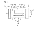
Außerdem enthält die Ätzkammer einen oder mehrere nicht dargestellte Gaseinlassöffnungen, in die ein Gasgemisch aus Argon, Helium, Schwefelhexafluorid SF6 und Sauerstoff einströmt. Durch eine oder mehrere nicht dargestellte Gasauslassöffnungen strömen ein Teil des eingelassenen Gasgemisches sowie Reaktionsprodukte wieder aus.In addition, the etching chamber contains one or more gas inlet openings, not shown, into which a gas mixture of argon, helium, sulfur hexafluoride SF 6 and oxygen flows. Through one or more gas outlet openings, not shown, a part of the admitted gas mixture and reaction products flow out again.
Die Plasmaätzanlage enthält außerdem eine oberhalb der Ätzkammer oder im oberen Bereich der Ätzkammer angeordnete Spule 24 mit Windungen 30 bis 44. Ein Anschluss der Spule ist mit einer Wechselspannungsquelle 50 über eine Leitung 52 leitfähig verbunden. Der andere Anschluss der Wechselspannungsquelle 50 liegt auf einem Massepotential M. Die Frequenz der Wechselspannungsquelle 50 beträgt 13,56 MHz. Die Wechselspannungsquelle 50 verbraucht eine Leistung von 600 Watt, um das Plasma 12 zu erzeugen.The plasma etching system also includes a coil 24 with
Weiterhin enthält die Plasmaätzanlage 10 eine Wechselspannungsquelle 60, die mit einer Frequenz von 13,56 MHz betrieben wird. Der eine Anschluss der Wechselspannungsquelle 60 ist über eine elektrisch leitfähige Leitung 62 mit dem elektrisch leitfähigen Substratträger 20 verbunden. Der andere Anschluss der Wechselspannungsquelle 60 ist mit dem Massepotential M verbunden. Die Wechselspannungsquelle 60 erzeugt eine Substratvorspannung von -220 Volt unter einem Leistungsverbrauch von bspw. 70 Watt.Furthermore, the
Die Wechselspannungsquellen 50 und 60 sind unabhängig voneinander steuerbar, so dass sich die Ionendichte und die Ionenenergie unabhängig voneinander regeln lassen. Weiterhin lässt sich die Relation geladener Teilchen zu ungeladenen Teilchen vorgeben.The
Zum Ätzen des Loches 72, das auch in
- Gasdruck 120 µbar,
- Plasmaleistung 600 Watt,
- Substratvorspannung -220 Volt
Heliumgasfluss 126 sccm,Sauerstoffgasfluss 32 sccm,- Schwefelhexafluoridgasfluss 59 sccm, und
Argongasfluss 84 sccm.
- Gas pressure 120 μbar,
- Plasma power 600 watts,
- Substrate bias -220 volts
-
Helium gas flow 126 sccm, -
Oxygen gas flow 32 sccm, - Sulfur hexafluoride gas flow 59 sccm, and
-
Argon gas flow 84 sccm.
Damit wurden folgende Ätzergebnisse erreicht:
- Lochtiefe T: 75 Mikrometer,
- Lochdurchmesser an der Öffnung 76: 10 Mikrometer,
- geöffnete Fläche: 4 % (3 % bis 5 %),
- Neigungswinkel W1 der Seitenwand 76: 87 °,
- bzw. Neigungswinkel W2 der Seitenwand 76: 93°, und
- Ätzrate: 6 Mikrometer/Minute.
- Hole depth T: 75 microns,
- Hole diameter at the opening 76: 10 microns,
- open area: 4% (3% to 5%),
- Inclination angle W1 of the side wall 76: 87 °,
- or inclination angle W2 of the side wall 76: 93 °, and
- Etching rate: 6 microns / minute.
In der Ätzkammer laufen unter anderem die folgenden Reaktionen bzw. Vorgänge ab:
- Ionen, insbesondere Kationen 80, 82 werden aus dem Plasma auf Grund der Substratvorspannung
bis zum Lochboden 78 beschleunigt und verhindern dort die Bildung eines Siliziumdioxidfilms. - unter der Einwirkung des Plasmas 12 bilden sich aus dem Schwefelhexafluorid SF6 Fluorradikale F*, siehe
Pfeil 84, und Schwefelradikale, - unter der Einwirkung des Plasmas 12 bilden sich aus dem molekularen Sauerstoff Sauerstoffradikale O*, siehe
Pfeil 86, - Die Schwefelradikale und eine Teil der Sauerstoffradikale O* reagieren zu Schwefeloxidverbindungen SO×, z.B. zu Schwefelmonoxid SO oder zu Schwefeldioxid SO2, siehe
Pfeile 88und 90, - Fluorradikale F* reagieren mit dem Silizium des Siliziumsubstrates 22 an noch nicht oder noch nicht ausreichend mit Siliziumdioxid bedeckten Stellen der Seitenwand 76, insbesondere in der Nähe des Grabenbodens 78, siehe
Pfeil 92, mit demSilizium am Grabenboden 78, siehePfeil 94. Dabei entstehen Siliziumfluorverbindungen SiF×, z.B. Siliziumtetrafluorid SiF4, siehe Pfeile 96und 98, - Ein anderer Teil der Sauerstoffradikale O* reagiert mit den Siliziumfluorverbindungen SiF× zu Siliziumdioxid SiO2, das sich an
der Seitenwand 76 ablagert,siehe Pfeile und 104. Andere Sauerstoffradikale O* reagieren auch direkt mit dem Silizium des Siliziumsubstrates 22 zu Siliziumdioxid SiO2.
- Ions, in
particular cations - under the action of the plasma 12, sulfur hexafluoride SF 6 forms fluorine radicals F *, see
arrow 84, and sulfur radicals, - under the action of the plasma 12, oxygen radicals O * are formed from the molecular oxygen, see
arrow 86, - The sulfur radicals and a part of the oxygen radicals O * react to form sulfur oxide SO x, such as SO to sulfur monoxide or sulfur dioxide SO 2, see
arrows - Fluorine radicals F * react with the silicon of the
silicon substrate 22 at sites of thesidewall 76 which are not yet or not sufficiently covered with silicon dioxide, in particular in the vicinity of the trench bottom 78, seearrow 92, with the silicon at the trench bottom 78, seearrow 94 Silicon fluoride compounds SiF × , eg silicon tetrafluoride SiF 4, seearrows - Another part of the oxygen radical O * reacts with the silicon fluoride compounds SiF × to silica SiO 2 deposited on the
sidewall 76, seearrows silicon substrate 22 to form silica SiO 2 .
Eine Nachzeichnung eines SEM-Bildes (Secundary Electron Microscopy) entlang eines Querschnitts durch das Loch 72 ist in
- Gasdruck 93 µbar,
- Plasmaleistung 700 Watt,
- Substratvorspannung -200 Volt,
- Heliumgasfluss 131 sccm,
- Sauerstoffgasfluss 35 sccm,
- Schwefelhexafluoridgasfluss 53 sccm, und
- Argongasfluss 131 sccm.
- Gas pressure 93 μbar,
- Plasma power 700 watts,
- Substrate bias voltage -200 volts,
- Helium gas flow 131 sccm,
- Oxygen gas flow 35 sccm,
- Sulfur hexafluoride gas flow 53 sccm, and
- Argon gas flow 131 sccm.
Damit wurden folgende Ätzergebnisse erreicht:
- Lochtiefe T: 56 Mikrometer,
- Lochdurchmesser an der Öffnung: 10 Mikrometer,
- geöffnete Fläche: 4 % (3 % bis 5 %),
- Neigungswinkel W1 der Seitenwand 76: 89 °,
- bzw. Neigungswinkel W2 der Seitenwand 76: 91°, und
- Ätzrate: 4,5 Mikrometer/Minute.
- Hole depth T: 56 microns,
- Hole diameter at the opening: 10 microns,
- open area: 4% (3% to 5%),
- Inclination angle W1 of the side wall 76: 89 °,
- or inclination angle W2 of the side wall 76: 91 °, and
- Etch rate: 4.5 microns / minute.
- Gasdruck 120 µbar,
- Plasmaleistung 800 Watt,
- Substratvorspannung -220 Volt,
- Heliumgasfluss 112 sccm,
Sauerstoffgasfluss 50 sccm,- Schwefelhexafluoridgasfluss 66 sccm, und
- Argongasfluss 168 sccm.
- Gas pressure 120 μbar,
- Plasma power 800 watts,
- Substrate bias voltage -220 volts,
- Helium gas flow 112 sccm,
-
Oxygen gas flow 50 sccm, - Sulfur hexafluoride gas flow 66 sccm, and
- Argon gas flow 168 sccm.
Damit wurden folgende Ätzergebnisse erreicht:
- Lochtiefe T: 68 Mikrometer,
- Lochdurchmesser an der Öffnung: 10 Mikrometer,
- geöffnete Fläche: 4 % (3 % bis 5 %),
- Neigungswinkel W1 der Seitenwand 76: 88 °,
- bzw. Neigungswinkel W2 der Seitenwand 76: 92°, und
- Ätzrate: 5 Mikrometer/Minute.
- Hole depth T: 68 microns,
- Hole diameter at the opening: 10 microns,
- open area: 4% (3% to 5%),
- Inclination angle W1 of the side wall 76: 88 °,
- or inclination angle W2 of the side wall 76: 92 °, and
- Etching rate: 5 microns / minute.
Die Ausführungsbeispiele wurden für eine TCP-Prozesskammer (Transformer Coupled Plasma) erläutert. Solche Kammern werden u.a. auch als ICP- (Inductive Coupled Plasma source), IPS-(Inductive Coupled plasma Source) oder als DPS-Kammer (Decoupled Plasma Source) bezeichnet. Die Anlagen erzeugen ein HDP (High Density Plasma) mit mindestens 1010 Ionen pro Kubikzentimeter, vorzugsweise im Bereich zwischen 1011 Ionen/cm3 und 1012 Ionen/cm3.The embodiments have been explained for a TCP process chamber (Transformer Coupled Plasma). Such chambers are also known as ICP (Inductive Coupled Plasma), IPS (Inductive Coupled Plasma Source) or DPS (Decoupled Plasma Source). The plants produce a HDP (High Density Plasma) with at least 10 10 ions per cubic centimeter, preferably in the range between 10 11 ions / cm 3 and 10 12 ions / cm 3 .
Claims (18)
- Method for anisotropically etching a recess (72) in a silicon substrate (22),
in which a plasma is used for energetic excitation of a reactive etching gas,
in which the reactive etching gas is a constituent of a continuous gas flow,
and in which at least one recess (72) is deepened by at least seventy-five micrometers or by at least one hundred micrometers without interrupting the gas flow in the meantime,
wherein the reactive etching gas contains a fluorine-free additional gas, namely an oxide forming agent, and wherein the etching gas is diluted with only one inert gas or noble gas or with a plurality of inert gases or noble gases,
and wherein the proportion contributed by the fluorine-free additional gas in the total active gas flow lies between 30% and 40%,
and wherein the proportion contributed by the gas flow of reactive etching gas in the total gas flow lies in the range of between 25% and 35%,
and wherein an etching mask (70) made of silicon dioxide is used for defining the position of the recess (72),
and wherein the composition of the gas flow remains the same during the etching of the recess (72). - Method according to Claim 1, characterized in that the reactive etching gas contains fluorine or fluorine compounds, preferably sulfur hexafluoride SF6 and/or nitrogen trifluoride NF3, in particular only one type of fluorine compounds.
- Method according to Claim 1 or 2, characterized in that the reactive gas contains molecular oxygen, and/or in that the proportion contributed by the fluorine-free additional gas, in particular the proportion contributed by the oxygen gas flow, in the total active gas flow is 35%.
- Method according to one of the preceding claims, characterized in that the etching gas contains helium or argon, or in that the etching gas contains helium and argon,
and/or in that the proportion contributed by the argon gas flow in the total inert gas flow lies between 25% and 65% or between 35% and 55%. - Method according to one of the preceding claims, characterized in that the proportion contributed by the gas flow comprising reactive etching gas in the total gas flow lies in the range of between 28% and 32%.
- Method according to one of the preceding clams, characterized in that the method according to one of the preceding claims, characterized in that the pressure during etching is greater than 0.05 mbar or greater than 0.1 mbar,
and in that the pressure during etching is preferably less than 0.5 mbar or less than 0.25 mbar. - Method according to one of the preceding claims, characterized in that the plasma is generated with powers of between 300 watts and 1200 watts or between 500 watts and 1000 watts, in particular with 600 watts, and in that the frequency for generating the plasma is preferably less than 100 MHz.
- Method according to one of the preceding claims, characterized in that a substrate voltage is generated with powers of greater than 50 watts or greater than 60 watts, preferably with powers of greater than 70 watts,
the power preferably being less than 700 watts, and/or in that a substrate bias voltage is generated with a magnitude of greater than 150 volts or greater than 180 volts or greater than 210 volts, the substrate bias voltage having a magnitude preferably less than 600 volts,
and in that the frequency for generating the substrate bias voltage is preferably less than 100 MHz. - Method according to one of the preceding claims, characterized in that the following values hold true or in that values hold true which deviate by at most plus or minus five percent or by at most plus or minus ten percent from the values stated:gas pressure 120 µbar,plasma power 600 watts,substrate bias voltage -220 volts,helium gas flow 126 sccm,oxygen gas flow 32 sccm,sulfur hexafluoride gas flow 59 sccm,argon gas flow 84 sccm,preferably no further gases being used,or in that the following values hold true or in that values hold true which deviate by at most plus or minus five percent or by at most plus or minus ten percent from the values stated:gas pressure 93 µbar,plasma power 700 watts,substrate bias voltage -200 volts,helium gas flow 131 sccm,oxygen gas flow 35 sccm,sulfur hexafluoride gas flow 53 sccm,argon gas flow 131 sccm,preferably no further gases being used,or in that the following values hold true or in that values hold true which deviate by at most plus or minus five percent or by at most plus or minus ten percent from the values stated:gas pressure 120 µbar,plasma power 800 watts,substrate bias voltage -220 volts,helium gas flow 112 sccm,oxygen gas flow 50 sccm,sulfur hexafluoride gas flow 66 sccm,argon gas flow 168 sccm,preferably no further gases being used.
- Method according to one of the preceding claims, characterized in that the recess (72) is a trench or a hole,
and/or in that the aspect ratio between the smallest lateral dimension at the edge of the recess (72) and the continuously etched depth (T) of the recess (72) is greater than 8:1 or greater than 10:1,
and/or in that the smallest lateral dimension at the edge of the cutout (72) is less than twenty micrometers or less than ten micrometers,
and/or in that the proportion made up by the opening of the recess (72) or the openings of the recess (72) relative to the size of the original substrate surface into which the recess (72) is introduced is less than 20% or less than 10% or less than 5%. - Method according to one of the preceding claims, characterized in that the angle (W2) of inclination of a wall of a recess that tapers with increasing distance from the substrate surface with respect to the substrate surface containing the edge of the cutout is greater than 91 degrees, greater than 92 degrees or greater than 93 degrees, the angle (W2) of inclination preferably being less than 110 degrees, and the angle (W2) of inclination preferably being set by way of an oxygen proportion in the process gas.
- Method according to one of the preceding claims, characterized in that no silicon-containing gas is introduced externally into an etching chamber utilized for etching.
- Method according to Claim 12, characterized in that the gas is not a gas with compounds containing silicon and fluorine.
- Method according to one of the preceding claims, characterized in that the total gas flow lies between 200 and 500 sccm or between 250 and 350 sccm, preferably between 295 and 305 sccm,
and/or in that the chamber volume of the etching chamber is 30 liters, or in that the total gas flow is converted to a different chamber volume with residence times remaining the same. - Use of a plasma etching system (10) in a method according to one of the preceding claims, for the etching of at least one recess (72) having a depth (T) of greater than fifty micrometers or greater than seventy-five micrometers or greater than one hundred micrometers with continuous gas flow without gases which flow into an etching chamber of the plasma etching system (10) being interrupted in the meantime.
- Use according to Claim 15, characterized in that the plasma etching system does not contain a control unit for cyclic etching.
- Use according to Claim 15 or 16, characterized in that the magnitude of the gas flow remains the same during the etching of the recess.
- Use according to one of Claims 15 to 17, characterized in that the plasma etching system (10) contains a plasma source (24, 50), into which energy is coupled inductively or by radiating in microwave radiation,
and/or in that the plasma etching system (10) is a system of the type Lam TCP 9400 PTX.
Applications Claiming Priority (2)
| Application Number | Priority Date | Filing Date | Title |
|---|---|---|---|
| DE10331526A DE10331526A1 (en) | 2003-07-11 | 2003-07-11 | A method of anisotropically etching a recess in a silicon substrate and using a plasma etching |
| PCT/EP2004/051285 WO2005008760A2 (en) | 2003-07-11 | 2004-06-29 | Method for anisotropically etching a recess in a silicon substrate and use of a plasma etching system |
Publications (2)
| Publication Number | Publication Date |
|---|---|
| EP1644954A2 EP1644954A2 (en) | 2006-04-12 |
| EP1644954B1 true EP1644954B1 (en) | 2013-05-08 |
Family
ID=33560059
Family Applications (1)
| Application Number | Title | Priority Date | Filing Date |
|---|---|---|---|
| EP04766096.4A Expired - Fee Related EP1644954B1 (en) | 2003-07-11 | 2004-06-29 | Method for anisotropically etching a recess in a silicon substrate and use of a plasma etching system |
Country Status (5)
| Country | Link |
|---|---|
| US (1) | US7799691B2 (en) |
| EP (1) | EP1644954B1 (en) |
| JP (2) | JP4988341B2 (en) |
| DE (1) | DE10331526A1 (en) |
| WO (1) | WO2005008760A2 (en) |
Families Citing this family (13)
| Publication number | Priority date | Publication date | Assignee | Title |
|---|---|---|---|---|
| JP5154013B2 (en) * | 2005-10-12 | 2013-02-27 | パナソニック株式会社 | Dry etching method |
| US7608195B2 (en) * | 2006-02-21 | 2009-10-27 | Micron Technology, Inc. | High aspect ratio contacts |
| JP5061506B2 (en) * | 2006-06-05 | 2012-10-31 | 富士電機株式会社 | Method for manufacturing silicon carbide semiconductor device |
| JP5135879B2 (en) * | 2007-05-21 | 2013-02-06 | 富士電機株式会社 | Method for manufacturing silicon carbide semiconductor device |
| JP5135885B2 (en) * | 2007-05-24 | 2013-02-06 | 富士電機株式会社 | Method for manufacturing silicon carbide semiconductor device |
| JP5309587B2 (en) * | 2008-02-07 | 2013-10-09 | 富士電機株式会社 | Trench etching method for silicon carbide semiconductor substrate |
| JP2009259863A (en) * | 2008-04-11 | 2009-11-05 | Tokyo Electron Ltd | Dry etching processing device, and dry etching method |
| JP5264383B2 (en) * | 2008-09-17 | 2013-08-14 | 東京エレクトロン株式会社 | Dry etching method |
| FR2956923A1 (en) * | 2010-03-01 | 2011-09-02 | St Microelectronics Tours Sas | VERTICAL POWER COMPONENT HIGH VOLTAGE |
| JP2013110139A (en) * | 2011-11-17 | 2013-06-06 | Tokyo Electron Ltd | Manufacturing method for semiconductor device |
| JP6533998B2 (en) * | 2015-05-13 | 2019-06-26 | 国立研究開発法人産業技術総合研究所 | Dry etching method |
| JP6575874B2 (en) * | 2016-03-09 | 2019-09-18 | パナソニックIpマネジメント株式会社 | Device chip manufacturing method |
| DE102016220248A1 (en) * | 2016-10-17 | 2018-04-19 | Fraunhofer-Gesellschaft zur Förderung der angewandten Forschung e.V. | APPARATUS AND METHOD FOR ANISOTROPIC DRY EQUIPMENT FLUORESCENT MIXING |
Citations (2)
| Publication number | Priority date | Publication date | Assignee | Title |
|---|---|---|---|---|
| US20010001743A1 (en) * | 1999-04-20 | 2001-05-24 | Mcreynolds Darrell | Mechanism for etching a silicon layer in a plasma processing chamber to form deep openings |
| WO2001047005A1 (en) * | 1999-12-20 | 2001-06-28 | Applied Materials, Inc. | Metal mask etching of silicon |
Family Cites Families (17)
| Publication number | Priority date | Publication date | Assignee | Title |
|---|---|---|---|---|
| FR2616030A1 (en) * | 1987-06-01 | 1988-12-02 | Commissariat Energie Atomique | PLASMA ETCHING OR DEPOSITION METHOD AND DEVICE FOR IMPLEMENTING THE METHOD |
| JPH04280427A (en) * | 1991-03-08 | 1992-10-06 | Fuji Electric Co Ltd | Processing of silicon substrate |
| JP3027864B2 (en) * | 1991-04-02 | 2000-04-04 | 富士電機株式会社 | Method for manufacturing semiconductor device |
| EP0729175A1 (en) * | 1995-02-24 | 1996-08-28 | International Business Machines Corporation | Method for producing deep vertical structures in silicon substrates |
| JP3351183B2 (en) * | 1995-06-19 | 2002-11-25 | 株式会社デンソー | Dry etching method and trench forming method for silicon substrate |
| DE19706682C2 (en) * | 1997-02-20 | 1999-01-14 | Bosch Gmbh Robert | Anisotropic fluorine-based plasma etching process for silicon |
| US5935874A (en) * | 1998-03-31 | 1999-08-10 | Lam Research Corporation | Techniques for forming trenches in a silicon layer of a substrate in a high density plasma processing system |
| WO1999067817A1 (en) * | 1998-06-22 | 1999-12-29 | Applied Materials, Inc. | Silicon trench etching using silicon-containing precursors to reduce or avoid mask erosion |
| US20020003126A1 (en) * | 1999-04-13 | 2002-01-10 | Ajay Kumar | Method of etching silicon nitride |
| JP2001024058A (en) | 1999-07-13 | 2001-01-26 | Matsushita Electronics Industry Corp | Method for formation of contact hole |
| US6440870B1 (en) * | 2000-07-12 | 2002-08-27 | Applied Materials, Inc. | Method of etching tungsten or tungsten nitride electrode gates in semiconductor structures |
| JP3920015B2 (en) * | 2000-09-14 | 2007-05-30 | 東京エレクトロン株式会社 | Si substrate processing method |
| JP4865951B2 (en) * | 2001-02-23 | 2012-02-01 | 東京エレクトロン株式会社 | Plasma etching method |
| US6887732B2 (en) * | 2001-05-07 | 2005-05-03 | Applied Materials, Inc. | Microstructure devices, methods of forming a microstructure device and a method of forming a MEMS device |
| JP3527901B2 (en) * | 2001-07-24 | 2004-05-17 | 株式会社日立製作所 | Plasma etching method |
| US6642127B2 (en) * | 2001-10-19 | 2003-11-04 | Applied Materials, Inc. | Method for dicing a semiconductor wafer |
| US20030082847A1 (en) * | 2001-10-26 | 2003-05-01 | I-Fire Technologies, Inc. | Method and apparatus for wafer thinning |
-
2003
- 2003-07-11 DE DE10331526A patent/DE10331526A1/en not_active Ceased
-
2004
- 2004-06-29 JP JP2006519909A patent/JP4988341B2/en not_active Expired - Fee Related
- 2004-06-29 EP EP04766096.4A patent/EP1644954B1/en not_active Expired - Fee Related
- 2004-06-29 WO PCT/EP2004/051285 patent/WO2005008760A2/en active Search and Examination
-
2006
- 2006-01-10 US US11/328,688 patent/US7799691B2/en not_active Expired - Fee Related
-
2012
- 2012-02-22 JP JP2012036687A patent/JP2012146991A/en active Pending
Patent Citations (3)
| Publication number | Priority date | Publication date | Assignee | Title |
|---|---|---|---|---|
| US20010001743A1 (en) * | 1999-04-20 | 2001-05-24 | Mcreynolds Darrell | Mechanism for etching a silicon layer in a plasma processing chamber to form deep openings |
| WO2001047005A1 (en) * | 1999-12-20 | 2001-06-28 | Applied Materials, Inc. | Metal mask etching of silicon |
| US6491835B1 (en) * | 1999-12-20 | 2002-12-10 | Applied Materials, Inc. | Metal mask etching of silicon |
Also Published As
| Publication number | Publication date |
|---|---|
| DE10331526A1 (en) | 2005-02-03 |
| JP4988341B2 (en) | 2012-08-01 |
| JP2009514192A (en) | 2009-04-02 |
| US20060175292A1 (en) | 2006-08-10 |
| EP1644954A2 (en) | 2006-04-12 |
| WO2005008760A2 (en) | 2005-01-27 |
| WO2005008760A3 (en) | 2005-06-09 |
| JP2012146991A (en) | 2012-08-02 |
| US7799691B2 (en) | 2010-09-21 |
Similar Documents
| Publication | Publication Date | Title |
|---|---|---|
| EP1644954B1 (en) | Method for anisotropically etching a recess in a silicon substrate and use of a plasma etching system | |
| EP0865664B1 (en) | Process for anisotropic plasma etching of different substrates | |
| DE69938342T2 (en) | METHOD FOR THE PRODUCTION OF CRACKS IN A SILICON LAYER OF A SUBSTRATE IN A PLASMA SYSTEM OF HIGH PLASMA DAMAGE | |
| DE10305602B4 (en) | Method and apparatus for generating a gas plasma and method for producing a semiconductor device | |
| DE69835032T2 (en) | IMPROVED METHOD TO EAT AN OXIDE LAYER | |
| EP0894338B1 (en) | Anisotropic, fluorine-based plasma etching method for silicon | |
| DE69909248T2 (en) | METHOD FOR REDUCING THE EROSION OF A MASK DURING A PLASMA ETCH | |
| DE4317623C2 (en) | Method and device for anisotropic plasma etching of substrates and their use | |
| DE69724192T2 (en) | Process for etching polycide structures | |
| DE2930290A1 (en) | METHOD FOR PRODUCING AN OBJECT | |
| EP1519895A1 (en) | Device and method for the production of chlorotrifluoride and system for etching semiconductor substrates using said device | |
| DE10249350A1 (en) | Device and method for anisotropic plasma etching of a substrate, in particular a silicon body | |
| DE102004001099A1 (en) | Oxidation process with high density plasma | |
| DE4107329C2 (en) | ||
| DE212007000107U1 (en) | Annular plasma chamber for processes with high gas flow rates | |
| DE4105103C2 (en) | ||
| EP1095400B1 (en) | Methods for plasma etching silicon | |
| DE69819023T2 (en) | METHOD OF ETCHING A CONDUCTIVE LAYER | |
| DE19746425A1 (en) | Insulator etching method for semiconductor manufacture | |
| DE102009028256B4 (en) | A method of etching silicon carbide using a plasma etching method and silicon carbide substrate | |
| DE19841964B4 (en) | Process for adjusting the etching speed in anisotropic plasma etching of lateral structures | |
| EP1287546A1 (en) | Plasma etching system | |
| DE10204222B4 (en) | Method for sidewall passivation in plasma etching | |
| DE19945140B4 (en) | Method for producing a mask layer with openings of reduced width | |
| DE10053780A1 (en) | Process for structuring a silicon oxide layer |
Legal Events
| Date | Code | Title | Description |
|---|---|---|---|
| PUAI | Public reference made under article 153(3) epc to a published international application that has entered the european phase |
Free format text: ORIGINAL CODE: 0009012 |
|
| 17P | Request for examination filed |
Effective date: 20051228 |
|
| AK | Designated contracting states |
Kind code of ref document: A2 Designated state(s): DE FR GB |
|
| RIN1 | Information on inventor provided before grant (corrected) |
Inventor name: SUBKE, KAI-OLAF Inventor name: HANEWALD, THORSTEN Inventor name: JANSSEN, INGOLD Inventor name: HAUSER, ANDREAS |
|
| DAX | Request for extension of the european patent (deleted) | ||
| RBV | Designated contracting states (corrected) |
Designated state(s): DE FR GB |
|
| 17Q | First examination report despatched |
Effective date: 20090618 |
|
| RAP1 | Party data changed (applicant data changed or rights of an application transferred) |
Owner name: INFINEON TECHNOLOGIES AG |
|
| REG | Reference to a national code |
Ref country code: DE Ref legal event code: R079 Ref document number: 502004014157 Country of ref document: DE Free format text: PREVIOUS MAIN CLASS: H01J0037320000 Ipc: H01L0021306500 |
|
| RIC1 | Information provided on ipc code assigned before grant |
Ipc: H01L 21/3065 20060101AFI20121119BHEP Ipc: H01J 37/32 20060101ALI20121119BHEP |
|
| GRAP | Despatch of communication of intention to grant a patent |
Free format text: ORIGINAL CODE: EPIDOSNIGR1 |
|
| GRAS | Grant fee paid |
Free format text: ORIGINAL CODE: EPIDOSNIGR3 |
|
| GRAA | (expected) grant |
Free format text: ORIGINAL CODE: 0009210 |
|
| AK | Designated contracting states |
Kind code of ref document: B1 Designated state(s): DE FR GB |
|
| REG | Reference to a national code |
Ref country code: GB Ref legal event code: FG4D Free format text: NOT ENGLISH |
|
| REG | Reference to a national code |
Ref country code: DE Ref legal event code: R096 Ref document number: 502004014157 Country of ref document: DE Effective date: 20130711 |
|
| PLBE | No opposition filed within time limit |
Free format text: ORIGINAL CODE: 0009261 |
|
| STAA | Information on the status of an ep patent application or granted ep patent |
Free format text: STATUS: NO OPPOSITION FILED WITHIN TIME LIMIT |
|
| 26N | No opposition filed |
Effective date: 20140211 |
|
| REG | Reference to a national code |
Ref country code: DE Ref legal event code: R097 Ref document number: 502004014157 Country of ref document: DE Effective date: 20140211 |
|
| REG | Reference to a national code |
Ref country code: FR Ref legal event code: PLFP Year of fee payment: 13 |
|
| REG | Reference to a national code |
Ref country code: FR Ref legal event code: PLFP Year of fee payment: 14 |
|
| REG | Reference to a national code |
Ref country code: FR Ref legal event code: PLFP Year of fee payment: 15 |
|
| PGFP | Annual fee paid to national office [announced via postgrant information from national office to epo] |
Ref country code: FR Payment date: 20200619 Year of fee payment: 17 |
|
| PGFP | Annual fee paid to national office [announced via postgrant information from national office to epo] |
Ref country code: GB Payment date: 20200625 Year of fee payment: 17 |
|
| PGFP | Annual fee paid to national office [announced via postgrant information from national office to epo] |
Ref country code: DE Payment date: 20210824 Year of fee payment: 18 |
|
| GBPC | Gb: european patent ceased through non-payment of renewal fee |
Effective date: 20210629 |
|
| PG25 | Lapsed in a contracting state [announced via postgrant information from national office to epo] |
Ref country code: GB Free format text: LAPSE BECAUSE OF NON-PAYMENT OF DUE FEES Effective date: 20210629 |
|
| PG25 | Lapsed in a contracting state [announced via postgrant information from national office to epo] |
Ref country code: FR Free format text: LAPSE BECAUSE OF NON-PAYMENT OF DUE FEES Effective date: 20210630 |
|
| REG | Reference to a national code |
Ref country code: DE Ref legal event code: R119 Ref document number: 502004014157 Country of ref document: DE |
|
| PG25 | Lapsed in a contracting state [announced via postgrant information from national office to epo] |
Ref country code: DE Free format text: LAPSE BECAUSE OF NON-PAYMENT OF DUE FEES Effective date: 20230103 |