EP1642332B1 - Die bonding - Google Patents
Die bonding Download PDFInfo
- Publication number
- EP1642332B1 EP1642332B1 EP04740528A EP04740528A EP1642332B1 EP 1642332 B1 EP1642332 B1 EP 1642332B1 EP 04740528 A EP04740528 A EP 04740528A EP 04740528 A EP04740528 A EP 04740528A EP 1642332 B1 EP1642332 B1 EP 1642332B1
- Authority
- EP
- European Patent Office
- Prior art keywords
- machining
- adhesive layer
- laser
- die
- singulated
- Prior art date
- Legal status (The legal status is an assumption and is not a legal conclusion. Google has not performed a legal analysis and makes no representation as to the accuracy of the status listed.)
- Expired - Lifetime
Links
Images
Classifications
-
- H—ELECTRICITY
- H10—SEMICONDUCTOR DEVICES; ELECTRIC SOLID-STATE DEVICES NOT OTHERWISE PROVIDED FOR
- H10P—GENERIC PROCESSES OR APPARATUS FOR THE MANUFACTURE OR TREATMENT OF DEVICES COVERED BY CLASS H10
- H10P72/00—Handling or holding of wafers, substrates or devices during manufacture or treatment thereof
- H10P72/70—Handling or holding of wafers, substrates or devices during manufacture or treatment thereof for supporting or gripping
- H10P72/74—Handling or holding of wafers, substrates or devices during manufacture or treatment thereof for supporting or gripping using temporarily an auxiliary support
- H10P72/7402—Wafer tapes, e.g. grinding or dicing support tapes
-
- H—ELECTRICITY
- H10—SEMICONDUCTOR DEVICES; ELECTRIC SOLID-STATE DEVICES NOT OTHERWISE PROVIDED FOR
- H10W—GENERIC PACKAGES, INTERCONNECTIONS, CONNECTORS OR OTHER CONSTRUCTIONAL DETAILS OF DEVICES COVERED BY CLASS H10
- H10W99/00—Subject matter not provided for in other groups of this subclass
-
- H—ELECTRICITY
- H10—SEMICONDUCTOR DEVICES; ELECTRIC SOLID-STATE DEVICES NOT OTHERWISE PROVIDED FOR
- H10P—GENERIC PROCESSES OR APPARATUS FOR THE MANUFACTURE OR TREATMENT OF DEVICES COVERED BY CLASS H10
- H10P95/00—Generic processes or apparatus for manufacture or treatments not covered by the other groups of this subclass
- H10P95/11—Separation of active layers from substrates
-
- H—ELECTRICITY
- H10—SEMICONDUCTOR DEVICES; ELECTRIC SOLID-STATE DEVICES NOT OTHERWISE PROVIDED FOR
- H10W—GENERIC PACKAGES, INTERCONNECTIONS, CONNECTORS OR OTHER CONSTRUCTIONAL DETAILS OF DEVICES COVERED BY CLASS H10
- H10W72/00—Interconnections or connectors in packages
- H10W72/30—Die-attach connectors
-
- H—ELECTRICITY
- H10—SEMICONDUCTOR DEVICES; ELECTRIC SOLID-STATE DEVICES NOT OTHERWISE PROVIDED FOR
- H10P—GENERIC PROCESSES OR APPARATUS FOR THE MANUFACTURE OR TREATMENT OF DEVICES COVERED BY CLASS H10
- H10P72/00—Handling or holding of wafers, substrates or devices during manufacture or treatment thereof
- H10P72/70—Handling or holding of wafers, substrates or devices during manufacture or treatment thereof for supporting or gripping
- H10P72/74—Handling or holding of wafers, substrates or devices during manufacture or treatment thereof for supporting or gripping using temporarily an auxiliary support
- H10P72/7416—Handling or holding of wafers, substrates or devices during manufacture or treatment thereof for supporting or gripping using temporarily an auxiliary support used during dicing or grinding
-
- H—ELECTRICITY
- H10—SEMICONDUCTOR DEVICES; ELECTRIC SOLID-STATE DEVICES NOT OTHERWISE PROVIDED FOR
- H10W—GENERIC PACKAGES, INTERCONNECTIONS, CONNECTORS OR OTHER CONSTRUCTIONAL DETAILS OF DEVICES COVERED BY CLASS H10
- H10W72/00—Interconnections or connectors in packages
- H10W72/01—Manufacture or treatment
- H10W72/013—Manufacture or treatment of die-attach connectors
- H10W72/01331—Manufacture or treatment of die-attach connectors using blanket deposition
-
- H—ELECTRICITY
- H10—SEMICONDUCTOR DEVICES; ELECTRIC SOLID-STATE DEVICES NOT OTHERWISE PROVIDED FOR
- H10W—GENERIC PACKAGES, INTERCONNECTIONS, CONNECTORS OR OTHER CONSTRUCTIONAL DETAILS OF DEVICES COVERED BY CLASS H10
- H10W72/00—Interconnections or connectors in packages
- H10W72/071—Connecting or disconnecting
- H10W72/073—Connecting or disconnecting of die-attach connectors
-
- H—ELECTRICITY
- H10—SEMICONDUCTOR DEVICES; ELECTRIC SOLID-STATE DEVICES NOT OTHERWISE PROVIDED FOR
- H10W—GENERIC PACKAGES, INTERCONNECTIONS, CONNECTORS OR OTHER CONSTRUCTIONAL DETAILS OF DEVICES COVERED BY CLASS H10
- H10W72/00—Interconnections or connectors in packages
- H10W72/071—Connecting or disconnecting
- H10W72/073—Connecting or disconnecting of die-attach connectors
- H10W72/07331—Connecting techniques
- H10W72/07337—Connecting techniques using a polymer adhesive, e.g. an adhesive based on silicone or epoxy
Definitions
- This invention relates to die bonding.
- the wafer 11 and the DAF 12 are singulated to form a singulated die and DAF 15, as shown in Figure 2, as in dicing a wafer without a DAF, by cutting a channel 14 through the wafer and DAF and leaving a shallow trench 16 in the base film carrier tape 13.
- dicing of a wafer with a DAF uses a mechanical saw but using higher speed revolution of a dicing saw blade than used to dice a wafer without a DAF, to avoid the adhesive layer adhering to the saw blade.
- high-speed mechanical cutting tends to cause delamination of the DAF and base film and to create burrs, resulting in yield loss.
- Burrs created by the mechanical saw can be millimetre long strands of the adhesive layer. These strands may come into contact with an upper surface of the die, either by being carried to the upper surface by the saw blade or in subsequent handling and, in particular, may interfere with a die attach process.
- adhesive is placed on individual die after mechanical saw dicing in order to avoid the problems associated with delamination when using a DAF and creation of burrs. This process is extremely time consuming and inefficient.
- US-B-6 319 754 discloses a method of die bonding with a wafer, a double adhesive layer and a carrier base. A saw blade cuts the wafer and the double adhesive layer, and the two adhesives are separated by deforming the carrier base.
- the present invention is defined by a method according to claim 1 and an apparatus according to claim 16.
- the step of laser machining comprises laser machining the wafer substrate using a first laser beam with a first machining profile of selected laser pulse power, laser pulse repetition rate, laser pulse width, laser beam scanning speed and laser wavelength; using a second laser beam with a second such machining profile to machine the adhesive layer and using a third laser beam with a third such machining profile to machine the carrier base means such that a speed of machining is maximised while providing a predetermined quality of singulated dies without substantial delamination of the adhesive layer and the carrier base means or substantial production of burrs.
- At least two of the first machining profile, the second machining profile and the third machining profile are a same machining profile.
- the step of curing the structure comprises curing with ultraviolet light.
- the step of curing the attached singulated adhesive layer comprises heat curing the adhesive layer.
- the step of machining the wafer substrate comprises machining a blind via in the wafer substrate or a via through the wafer substrate and a die attach film.
- the step of laser machining includes a further step, after laser machining, of washing the structure to remove accumulated laser machining debris from the singulated die.
- the step of providing a structure comprises providing a structure having a protective film to protect the structure from debris produced during laser machining and the step of washing the structure comprises removing the protective film and accumulated debris thereon.
- the step of providing a structure comprises providing a structure having a wafer substrate less than 800 microns thick.
- the step of laser machining comprises providing an assist gas environment for laser machining.
- the step of providing an assist gas environment comprises providing a gas environment in which photo-dissociation produces active radicals.
- the step of providing a gas environment reduces deposition of solid machining debris around a laser-machining site.
- the carrier base means is one of: a dicing tape, an inflexible tape suitable for thin wafer dicing or backgrinding; and a glass or other transparent solid.
- the step of providing a structure comprises providing a structure including a wafer substrate separated facedown from substantially inflexible transparent backgrinding tape means by the adhesive layer and the step of laser machining is performed subsequent to backgrinding the wafer substrate.
- the step of picking and placing the die and attached singulated adhesive layer comprises picking and placing the die and attached singulated adhesive layer on another die to form a multistack die package.
- die bonding apparatus comprising: laser machining means for machining a wafer substrate and an adhesive layer attached to the wafer substrate and for no more than at most scribing underlying carrier base means to form a singulated die with a singulated adhesive layer; first curing means for curing the carrier base means to release the singulated adhesive layer from the carrier base means; pick and place means for picking the singulated die and adhesive layer from the carrier base means and placing the singulated die and adhesive layer on die pad means and second curing means for curing the singulated adhesive layer of the singulated die to adhere the singulated die to the die pad means.
- the laser machining means comprises: laser source means for providing a pulsed laser beam; laser beam scanning means; and control means for controlling at least one of laser pulse energy, laser wavelength, laser repetition frequency, laser pulse width, laser beam scanning speed and a number of scans by the pulsed laser beam.
- the laser machining means further comprises memory means for storing a machining profile of at least one of laser pulse energy, laser wavelength, laser repetition frequency, laser pulse width, laser beam scanning speed and a number of scans by the pulsed laser beam, for use by the control means.
- the first curing means comprises ultraviolet curing means.
- the second curing means comprises heat curing means.
- the die bonding apparatus includes washing means for washing laser machining debris from the singulated die.
- the wafer substrate is provided with a protective film to protect the wafer substrate from laser machining debris, and the washing means is arranged to remove the protective film from the singulated die.
- the die bonding apparatus is adapted for carrier base means which is one of: a dicing tape, an inflexible tape suitable for thin wafer dicing or backgrinding; and a glass or other transparent solid.
- the die bonding apparatus is adapted for machining a structure comprising a wafer substrate separated facedown from substantially inflexible transparent backgrinding tape means by the adhesive layer.
- a laser beam 31, 32, 33 to dice a structure 10 comprising a wafer 11 with a DAF 12 mounted on a carrier base 13, it is possible to machine through the wafer and the DAF without causing substantially any delamination of the adhesive layer 12 and carrier base 13 or causing substantially any burrs, from, for example, the adhesive layer 12.
- the carrier base 13 may be, for example, any known carrier film as used in industry, a substantially inflexible support used in thin film dicing or backgrinding or a glass or other transparent solid.
- the carrier base may an inflexible transparent backgrinding tape with the wafer mounted facedown on the backgrinding tape for dicing after a backgrinding process.
- each layer 11, 12, 13 is scanned with a predetermined number of one or more scans with predetermined machining parameters dependent on a known thickness and known machinability of material of the layer.
- a nature of a material being machined and interfaces between layers may be determined by observation of machining characteristics.
- the parameters may be determined empirically from samples of wafers to be machined.
- all machining of the wafer may be performed before all machining of the adhesive layer, which may be performed before all machining of the carrier base or each dice lane may be completely machined in turn, or a combination of such strategies may be used.
- a single cutting strategy or machining profile is used to cut two or all three layers 11, 12, 13, using an optimised machining profile for a combination of such layers.
- a known translation table may be provided to allow access of the laser beam to all parts of the wafer to be machined.
- laser machining process has been described as conveniently scribing the carrier base, it will be understood that alternatively laser machining may be halted at an interface of the adhesive layer and carrier base, without significantly, or at all, scribing the carrier base.
- the laser machining process of the invention has been found to be suitable for wafers up to 800 ⁇ m thick.
- This laser machining process is suitable not only for dicing wafers but also for machining via structures in wafers with a DAF.
- the laser machining process of the invention may optionally be performed, in a known manner, in an active gas environment or in a gas environment where photo-dissociation produces active radicals.
- Laser machining in a suitable active gas environment changes a chemical nature of debris produced.
- a chemical reaction between a suitable active gas and the debris while in a molten state results in removal of debris in gaseous form, with consequentially reduced deposition of solid debris around a laser machining site.
- the singulated die may be washed to remove debris produced during laser machining, before curing of the DAF.
- the wafer substrate may be protected from such debris by a protective film and the protective film and accumulated debris may be removed by washing.
- die bonding of a singulated die proceeds substantially as in the prior art.
- the carrier base 13, or an adhesive, not shown, between the carrier base, tape or film and the adhesive layer, is cured with ultraviolet light to release the singulated die 15 from the carrier tape or film 13.
- the singulated die 15 is picked from the carrier base, tape or film 13 and placed on a die pad. Alternatively, the die 15 may be picked and placed on another die to form a multistack die package.
- the adhesive layer on the singulated die 15 is heat cured to adhere the singulated die to the die pad, or another die, for further known processing.
Landscapes
- Dicing (AREA)
- Die Bonding (AREA)
- Laser Beam Processing (AREA)
- Light Receiving Elements (AREA)
Abstract
Description
- This invention relates to die bonding.
- The use of dies with die attach films (DAF) transported on a base material carrier tape to provide direct bonding of dies to a die pad is well known in the microelectronics industry. On picking up a singulated die from the carrier tape, an adhesive layer is carried on a lower surface of the die and, after placing the die on a die pad, the adhesive layer is cured by heating to adhere the die to the die pad. A cross-section of such a
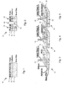
structure 10 of awafer 11 mounted on a DAFadhesive layer 12 andcarrier base 13 before dicing is shown on Figure 1. Thewafer 11 and theDAF 12 are singulated to form a singulated die andDAF 15, as shown in Figure 2, as in dicing a wafer without a DAF, by cutting achannel 14 through the wafer and DAF and leaving ashallow trench 16 in the basefilm carrier tape 13. - Known dicing of a wafer with a DAF uses a mechanical saw but using higher speed revolution of a dicing saw blade than used to dice a wafer without a DAF, to avoid the adhesive layer adhering to the saw blade. However, such high-speed mechanical cutting tends to cause delamination of the DAF and base film and to create burrs, resulting in yield loss. Burrs created by the mechanical saw can be millimetre long strands of the adhesive layer. These strands may come into contact with an upper surface of the die, either by being carried to the upper surface by the saw blade or in subsequent handling and, in particular, may interfere with a die attach process. In some cases, adhesive is placed on individual die after mechanical saw dicing in order to avoid the problems associated with delamination when using a DAF and creation of burrs. This process is extremely time consuming and inefficient.
-
US-B-6 319 754 discloses a method of die bonding with a wafer, a double adhesive layer and a carrier base. A saw blade cuts the wafer and the double adhesive layer, and the two adhesives are separated by deforming the carrier base. - It is an object of the present invention at least to ameliorate the aforesaid difficulties in the prior art.
- The present invention is defined by a method according to
claim 1 and an apparatus according toclaim 16. - Preferably, the step of laser machining comprises laser machining the wafer substrate using a first laser beam with a first machining profile of selected laser pulse power, laser pulse repetition rate, laser pulse width, laser beam scanning speed and laser wavelength; using a second laser beam with a second such machining profile to machine the adhesive layer and using a third laser beam with a third such machining profile to machine the carrier base means such that a speed of machining is maximised while providing a predetermined quality of singulated dies without substantial delamination of the adhesive layer and the carrier base means or substantial production of burrs.
- Conveniently, at least two of the first machining profile, the second machining profile and the third machining profile are a same machining profile.
- Advantageously, the step of curing the structure comprises curing with ultraviolet light.
- Conveniently, the step of curing the attached singulated adhesive layer comprises heat curing the adhesive layer.
- Advantageously, the step of machining the wafer substrate comprises machining a blind via in the wafer substrate or a via through the wafer substrate and a die attach film.
- Preferably, the step of laser machining includes a further step, after laser machining, of washing the structure to remove accumulated laser machining debris from the singulated die.
- Conveniently, the step of providing a structure comprises providing a structure having a protective film to protect the structure from debris produced during laser machining and the step of washing the structure comprises removing the protective film and accumulated debris thereon.
- Advantageously, the step of providing a structure comprises providing a structure having a wafer substrate less than 800 microns thick.
- Preferably, the step of laser machining comprises providing an assist gas environment for laser machining.
- Advantageously, the step of providing an assist gas environment comprises providing a gas environment in which photo-dissociation produces active radicals.
- Preferably, the step of providing a gas environment reduces deposition of solid machining debris around a laser-machining site.
- Conveniently, the carrier base means is one of: a dicing tape, an inflexible tape suitable for thin wafer dicing or backgrinding; and a glass or other transparent solid.
- Advantageously, the step of providing a structure comprises providing a structure including a wafer substrate separated facedown from substantially inflexible transparent backgrinding tape means by the adhesive layer and the step of laser machining is performed subsequent to backgrinding the wafer substrate.
- Alternatively, the step of picking and placing the die and attached singulated adhesive layer comprises picking and placing the die and attached singulated adhesive layer on another die to form a multistack die package.
- According to a second aspect of the present invention, there is provided die bonding apparatus comprising: laser machining means for machining a wafer substrate and an adhesive layer attached to the wafer substrate and for no more than at most scribing underlying carrier base means to form a singulated die with a singulated adhesive layer; first curing means for curing the carrier base means to release the singulated adhesive layer from the carrier base means; pick and place means for picking the singulated die and adhesive layer from the carrier base means and placing the singulated die and adhesive layer on die pad means and second curing means for curing the singulated adhesive layer of the singulated die to adhere the singulated die to the die pad means.
- Preferably, the laser machining means comprises: laser source means for providing a pulsed laser beam; laser beam scanning means; and control means for controlling at least one of laser pulse energy, laser wavelength, laser repetition frequency, laser pulse width, laser beam scanning speed and a number of scans by the pulsed laser beam.
- Advantageously, the laser machining means further comprises memory means for storing a machining profile of at least one of laser pulse energy, laser wavelength, laser repetition frequency, laser pulse width, laser beam scanning speed and a number of scans by the pulsed laser beam, for use by the control means.
- Preferably, the first curing means comprises ultraviolet curing means.
- Advantageously, the second curing means comprises heat curing means.
- Conveniently, the die bonding apparatus includes washing means for washing laser machining debris from the singulated die.
- Advantageously, the wafer substrate is provided with a protective film to protect the wafer substrate from laser machining debris, and the washing means is arranged to remove the protective film from the singulated die.
- Conveniently, the die bonding apparatus is adapted for carrier base means which is one of: a dicing tape, an inflexible tape suitable for thin wafer dicing or backgrinding; and a glass or other transparent solid.
- Advantageously, the die bonding apparatus is adapted for machining a structure comprising a wafer substrate separated facedown from substantially inflexible transparent backgrinding tape means by the adhesive layer.
- The invention will now be described, by way of example, with reference to the accompanying drawings in which:
- Figure 1 is a vertical cross-section of a known wafer, adhesive layer and carrier film structure;
- Figure 2 is the vertical cross-section of Figure 1 after dicing;
- Figure 3 is a perspective schematic view of laser machining, according to the invention, of the wafer of the structure of Figure 1;
- Figure 4 is a perspective schematic view of laser machining, according to the invention, of the adhesive layer of the structure of Figure 1; and
- Figure 5 is a perspective schematic view of laser scribing, according to the invention, of the carrier film of the structure of Figure 1.
- In the Figures like reference numerals denote like parts.
- Referring to the Figures, using a
laser beam structure 10 comprising awafer 11 with aDAF 12 mounted on acarrier base 13, it is possible to machine through the wafer and the DAF without causing substantially any delamination of theadhesive layer 12 andcarrier base 13 or causing substantially any burrs, from, for example, theadhesive layer 12. - The
carrier base 13 may be, for example, any known carrier film as used in industry, a substantially inflexible support used in thin film dicing or backgrinding or a glass or other transparent solid. Alternatively, the carrier base may an inflexible transparent backgrinding tape with the wafer mounted facedown on the backgrinding tape for dicing after a backgrinding process. - Referring to Figures 3 to 5, by controlling critical machining parameters of pulse power, pulse repetition rate, pulse width, laser wavelength and laser beam scan speed of a
laser beam wafer 11 and theDAF 12 while only scribing thecarrier base 13 and perform complete singulation without problems of delamination and burr. These critical parameters of the laser beam can be optimised for eachlayer laser beam - In this case, each
layer - In order to optimise efficiency of singulation, all machining of the wafer may be performed before all machining of the adhesive layer, which may be performed before all machining of the carrier base or each dice lane may be completely machined in turn, or a combination of such strategies may be used.
- Alternatively, where machining quality of the individual layers may be sacrificed for overall processing speed, a single cutting strategy or machining profile is used to cut two or all three
layers - A known translation table may be provided to allow access of the laser beam to all parts of the wafer to be machined.
- Although the laser machining process has been described as conveniently scribing the carrier base, it will be understood that alternatively laser machining may be halted at an interface of the adhesive layer and carrier base, without significantly, or at all, scribing the carrier base.
- The laser machining process of the invention has been found to be suitable for wafers up to 800µm thick.
- This laser machining process is suitable not only for dicing wafers but also for machining via structures in wafers with a DAF.
- The laser machining process of the invention may optionally be performed, in a known manner, in an active gas environment or in a gas environment where photo-dissociation produces active radicals. Laser machining in a suitable active gas environment changes a chemical nature of debris produced. In particular, under suitable conditions, a chemical reaction between a suitable active gas and the debris while in a molten state results in removal of debris in gaseous form, with consequentially reduced deposition of solid debris around a laser machining site.
- Following singulation, the singulated die may be washed to remove debris produced during laser machining, before curing of the DAF. Alternatively, the wafer substrate may be protected from such debris by a protective film and the protective film and accumulated debris may be removed by washing.
- Once the structure has been machined, die bonding of a singulated die proceeds substantially as in the prior art. The
carrier base 13, or an adhesive, not shown, between the carrier base, tape or film and the adhesive layer, is cured with ultraviolet light to release the singulated die 15 from the carrier tape orfilm 13. The singulated die 15 is picked from the carrier base, tape orfilm 13 and placed on a die pad. Alternatively, thedie 15 may be picked and placed on another die to form a multistack die package. The adhesive layer on the singulated die 15 is heat cured to adhere the singulated die to the die pad, or another die, for further known processing.
Claims (24)
- A method of die bonding comprising the steps of: providing a structure (10) comprising a wafer substrate (11) separated from carrier base means (13) by an adhesive layer (12) adhered to the carrier base means by a first adhesive between the carrier base (13) and the adhesive layer (12); laser machining through the wafer substrate, the first adhesive and through the adhesive layer no more than at most to scribe the carrier base means to form a singulated die (15) with an attached singulated adhesive layer (12); curing the structure to release the attached singulated adhesive layer from the carrier base means by curing the first adhesive; picking and placing the die and attached singulated adhesive layer on a die pad; and curing the attached singulated adhesive layer to adhere the die to the die pad.
- A method as claimed in claim 1, wherein the step of laser machining comprises laser machining the wafer substrate (11) using a first laser beam (31) with a first machining profile of selected laser pulse power, laser pulse repetition rate, laser pulse width, laser beam scanning speed and laser wavelength; using a second laser beam (32) with a second such machining profile to machine the adhesive layer (12) and using a third laser beam (33) with a third such machining profile to machine the carrier base means (14) such that a speed of machining is maximised while providing a predetermined quality of singulated dies without substantial delamination of the adhesive layer and the carrier base means or substantial production of burrs.
- A method as claimed in claim 2, wherein at least two of the first machining profile, the second machining profile and the third machining profile are a same machining profile.
- A method as claimed in any of the preceding claims, wherein the step of curing the structure (10) comprises curing with ultraviolet light.
- A method as claimed in any of the preceding claims, wherein the step of curing the attached singulated adhesive layer (12) comprises heat curing the adhesive layer.
- A method as claimed in any of the preceding claims, wherein the step of machining the wafer substrate comprises machining a blind via (14) in the wafer substrate (11) or a via through the wafer substrate (11) and the adhesive layer (12).
- A method as claimed in any of the preceding claims, wherein the step of laser machining includes a further step, after laser machining, of washing the structure to remove accumulated laser machining debris from the singulated die (15).
- A method as claimed in claim 7, wherein the step of providing a structure comprises providing a structure having a protective film to protect the structure from debris produced during laser machining and the step of washing the structure comprises removing the protective film and accumulated debris thereon.
- A method as claimed in any of the preceding claims, wherein the step of providing a structure comprises providing a structure having a wafer substrate (11) less than 800 microns thick.
- A method as claimed in any of the preceding claims, wherein the step of laser machining comprises providing an assist gas environment for laser machining.
- A method as claimed in claim 10, wherein the step of providing an assist gas environment comprises providing a gas environment in which photo-dissociation produces active radicals.
- A method as claimed in claims 10 or 11, wherein the step of providing a gas environment reduces deposition of solid machining debris around a laser-machining site.
- A method as claimed in any of the preceding claims, wherein the carrier base means is one of: a dicing tape, an inflexible tape suitable for thin wafer dicing or backgrinding; and a glass or other transparent solid.
- A method as claimed in any of the preceding claims, wherein the step of providing a structure comprises providing a structure including a wafer substrate separated facedown from substantially inflexible transparent backgrinding tape means by the adhesive layer and the step of laser machining is performed subsequent to backgrinding the wafer substrate.
- A method as claimed in any of the preceding claims, wherein the step of picking and placing the die and attached singulated adhesive layer comprises picking and placing the die and attached singulated adhesive layer on another die to form a multistack die package.
- A die bonding apparatus comprising: laser machining means arranged for machining a wafer substrate (11) and an adhesive layer (12) adhered to the wafer substrate (11) and attached to carrier base means (13) by a first adhesive between the carrier base means (13) and the adhesive layer (12) and for no more than at most scribing underlying carrier base means (13) to form a singulated die with a singulated adhesive layer (15); first curing means arranged for curing the first adhesive to release the singulated adhesive layer (12) from the carrier base means (13); pick and place means arranged for picking the singulated die and adhesive layer (15) from the carrier base means (13) and placing the singulated die and adhesive layer (15) on die pad means and second curing means arranged for curing the singulated adhesive layer (12) of the singulated die to adhere the singulated die to the die pad means.
- A die bonding apparatus as claimed in claim 16, wherein the laser machining means comprises: laser source means arranged for providing a pulsed laser beam (31, 32, 33); laser beam scanning means; and control means arranged for controlling at least one of laser pulse energy, laser wavelength, laser repetition frequency, laser pulse width, laser beam scanning speed and a number of scans by the pulsed laser beam.
- A die bonding apparatus as claimed in claim 17, wherein the laser machining means further comprises memory means for storing a machining profile of at least one of laser pulse energy, laser wavelength, laser repetition frequency, laser pulse width, laser beam scanning speed and a number of scans by the pulsed laser beam, for use by the control means.
- A die bonding apparatus as claimed in any of claims 16 to 18, wherein the first curing means comprises ultraviolet curing means.
- A die bonding apparatus as claimed in any of claims 16 to 19, wherein the second curing means comprises heat curing means.
- A die bonding apparatus as claimed in any of claims 16 to 20, including washing means arranged for washing laser machining debris from the singulated die.
- A die bonding apparatus as claimed in claim 21, wherein the wafer substrate is provided with a protective film to protect the wafer substrate from laser machining debris, and the washing means is arranged to remove the protective film from the singulated die.
- A die bonding apparatus as claimed in any claims 16 to 22, adapted for carrier base means which is one of: a dicing tape, an inflexible tape suitable for thin wafer dicing or backgrinding; and a glass or other transparent solid.
- A die bonding apparatus as claimed in any claims 16 to 22, adapted for machining a structure comprising a wafer substrate separated facedown from substantially inflexible transparent backgrinding tape means by the adhesive layer.
Applications Claiming Priority (2)
| Application Number | Priority Date | Filing Date | Title |
|---|---|---|---|
| GB0315623A GB2404280B (en) | 2003-07-03 | 2003-07-03 | Die bonding |
| PCT/EP2004/007161 WO2005004226A1 (en) | 2003-07-03 | 2004-07-01 | Die bonding |
Publications (2)
| Publication Number | Publication Date |
|---|---|
| EP1642332A1 EP1642332A1 (en) | 2006-04-05 |
| EP1642332B1 true EP1642332B1 (en) | 2008-01-16 |
Family
ID=27741543
Family Applications (1)
| Application Number | Title | Priority Date | Filing Date |
|---|---|---|---|
| EP04740528A Expired - Lifetime EP1642332B1 (en) | 2003-07-03 | 2004-07-01 | Die bonding |
Country Status (11)
| Country | Link |
|---|---|
| US (1) | US7989320B2 (en) |
| EP (1) | EP1642332B1 (en) |
| JP (1) | JP4625804B2 (en) |
| KR (1) | KR101167894B1 (en) |
| CN (1) | CN1816908B (en) |
| AT (1) | ATE384335T1 (en) |
| DE (1) | DE602004011343T2 (en) |
| GB (1) | GB2404280B (en) |
| MY (1) | MY141475A (en) |
| TW (1) | TWI245376B (en) |
| WO (1) | WO2005004226A1 (en) |
Families Citing this family (30)
| Publication number | Priority date | Publication date | Assignee | Title |
|---|---|---|---|---|
| JP4659300B2 (en) | 2000-09-13 | 2011-03-30 | 浜松ホトニクス株式会社 | Laser processing method and semiconductor chip manufacturing method |
| US6676878B2 (en) | 2001-01-31 | 2004-01-13 | Electro Scientific Industries, Inc. | Laser segmented cutting |
| WO2003076119A1 (en) * | 2002-03-12 | 2003-09-18 | Hamamatsu Photonics K.K. | Method of cutting processed object |
| TWI326626B (en) | 2002-03-12 | 2010-07-01 | Hamamatsu Photonics Kk | Laser processing method |
| AU2003211763A1 (en) | 2002-03-12 | 2003-09-22 | Hamamatsu Photonics K.K. | Method for dicing substrate |
| TWI520269B (en) | 2002-12-03 | 2016-02-01 | 濱松赫德尼古斯股份有限公司 | Cutting method of semiconductor substrate |
| AU2003220847A1 (en) | 2003-03-12 | 2004-09-30 | Hamamatsu Photonics K.K. | Laser beam machining method |
| JP4532358B2 (en) * | 2005-06-15 | 2010-08-25 | 株式会社ディスコ | Manufacturing method of semiconductor chip |
| DE102005048153B4 (en) | 2005-10-06 | 2010-08-05 | Infineon Technologies Ag | Method for producing a semiconductor device with semiconductor chip and adhesive film |
| DE102005048826B3 (en) | 2005-10-10 | 2007-04-12 | Infineon Technologies Ag | Semiconductor component has pretensioned double-sided adhesive foil between back of semiconductor chip and chip connecting surface with circuit carrier to separate into individual areas without tools |
| DE102005050127B3 (en) | 2005-10-18 | 2007-05-16 | Infineon Technologies Ag | Method for applying a structure of joining material to the backs of semiconductor chips |
| JP2008235398A (en) * | 2007-03-19 | 2008-10-02 | Disco Abrasive Syst Ltd | Device manufacturing method |
| GB2458475B (en) * | 2008-03-18 | 2011-10-26 | Xsil Technology Ltd | Processing of multilayer semiconductor wafers |
| JP2009231779A (en) * | 2008-03-25 | 2009-10-08 | Lintec Corp | Method of manufacturing semiconductor device |
| US20100167471A1 (en) | 2008-12-30 | 2010-07-01 | Stmicroelectronics Asia Pacific Pte. Ltd. | Reducing warpage for fan-out wafer level packaging |
| US20110156239A1 (en) * | 2009-12-29 | 2011-06-30 | Stmicroelectronics Asia Pacific Pte Ltd. | Method for manufacturing a fan-out embedded panel level package |
| US8502367B2 (en) | 2010-09-29 | 2013-08-06 | Stmicroelectronics Pte Ltd. | Wafer-level packaging method using composite material as a base |
| US20160133486A1 (en) | 2014-11-07 | 2016-05-12 | International Business Machines Corporation | Double Layer Release Temporary Bond and Debond Processes and Systems |
| US10475764B2 (en) * | 2014-12-26 | 2019-11-12 | Taiwan Semiconductor Manufacturing Company, Ltd. | Die bonder and methods of using the same |
| WO2016175653A2 (en) * | 2015-04-28 | 2016-11-03 | Nederlandse Organisatie Voor Toegepast-Natuurwetenschappelijk Onderzoek Tno | Apparatus and method for soldering chips |
| KR102194727B1 (en) | 2015-04-29 | 2020-12-23 | 삼성전기주식회사 | Inductor |
| KR101797728B1 (en) | 2016-03-11 | 2017-11-16 | 삼성디스플레이 주식회사 | Display apparatus |
| US9916989B2 (en) | 2016-04-15 | 2018-03-13 | Amkor Technology, Inc. | System and method for laser assisted bonding of semiconductor die |
| US10269756B2 (en) * | 2017-04-21 | 2019-04-23 | Invensas Bonding Technologies, Inc. | Die processing |
| US10607861B2 (en) | 2017-11-28 | 2020-03-31 | Nxp B.V. | Die separation using adhesive-layer laser scribing |
| US10727219B2 (en) | 2018-02-15 | 2020-07-28 | Invensas Bonding Technologies, Inc. | Techniques for processing devices |
| US11742314B2 (en) | 2020-03-31 | 2023-08-29 | Adeia Semiconductor Bonding Technologies Inc. | Reliable hybrid bonded apparatus |
| US12550799B2 (en) | 2021-03-31 | 2026-02-10 | Adeia Semiconductor Bonding Technologies Inc. | Direct bonding methods and structures |
| CN113784513A (en) * | 2021-08-10 | 2021-12-10 | 信维通信(江苏)有限公司 | Circuit board forming method |
| US12604771B2 (en) | 2021-10-28 | 2026-04-14 | Adeia Semiconductor Bonding Technologies Inc. | Direct bonding methods and structures |
Family Cites Families (45)
| Publication number | Priority date | Publication date | Assignee | Title |
|---|---|---|---|---|
| US3637377A (en) | 1966-11-03 | 1972-01-25 | Teeg Research Inc | Method for making a pattern on a support member by means of actinic radiation sensitive element |
| BE756807A (en) | 1969-09-29 | 1971-03-29 | Motorola Inc | PROCESS FOR NON-PREFERENTIAL ENGRAVING OF SILICON BY A GAS MIXTURE, AND GAS MIXTURE FOR THIS ENGRAVING |
| US3811182A (en) | 1972-03-31 | 1974-05-21 | Ibm | Object handling fixture, system, and process |
| US3866398A (en) | 1973-12-20 | 1975-02-18 | Texas Instruments Inc | In-situ gas-phase reaction for removal of laser-scribe debris |
| US4331504A (en) | 1981-06-25 | 1982-05-25 | International Business Machines Corporation | Etching process with vibrationally excited SF6 |
| US4617086A (en) | 1982-03-19 | 1986-10-14 | International Business Machines Corporation | Rapid etching method for silicon by SF6 gas |
| US4566935A (en) | 1984-07-31 | 1986-01-28 | Texas Instruments Incorporated | Spatial light modulator and method |
| US4639572A (en) | 1985-11-25 | 1987-01-27 | Ibm Corporation | Laser cutting of composite materials |
| US4731158A (en) | 1986-09-12 | 1988-03-15 | International Business Machines Corporation | High rate laser etching technique |
| JPH0715087B2 (en) * | 1988-07-21 | 1995-02-22 | リンテック株式会社 | Adhesive tape and method of using the same |
| US5322988A (en) | 1990-03-29 | 1994-06-21 | The United States Of America As Represented By The Secretary Of The Navy | Laser texturing |
| US5266532A (en) | 1990-03-29 | 1993-11-30 | The United States Of America As Represented By The Secretary Of The Navy | Method for laser-assisted silicon etching using halocarbon ambients |
| US5762744A (en) * | 1991-12-27 | 1998-06-09 | Rohm Co., Ltd. | Method of producing a semiconductor device using an expand tape |
| JPH05291398A (en) | 1992-04-08 | 1993-11-05 | Sony Corp | Element substrate and liquid crystal display device manufacturing method |
| JPH07135441A (en) * | 1994-06-02 | 1995-05-23 | Sanyo Electric Co Ltd | Manufacture of surface acoustic wave element |
| JP3028741B2 (en) * | 1994-12-20 | 2000-04-04 | 日立電線株式会社 | Method and apparatus for cutting substrate material |
| US5597767A (en) * | 1995-01-06 | 1997-01-28 | Texas Instruments Incorporated | Separation of wafer into die with wafer-level processing |
| JP3438369B2 (en) * | 1995-01-17 | 2003-08-18 | ソニー株式会社 | Manufacturing method of member |
| KR970008386A (en) | 1995-07-07 | 1997-02-24 | 하라 세이지 | A method of dividing a substrate and a dividing device |
| IL115931A0 (en) | 1995-11-09 | 1996-01-31 | Oramir Semiconductor Ltd | Laser stripping improvement by modified gas composition |
| AUPN736195A0 (en) | 1995-12-29 | 1996-01-25 | Pacific Solar Pty Limited | Improved laser grooving method |
| JPH1140523A (en) * | 1997-07-22 | 1999-02-12 | Mitsubishi Electric Corp | Substrate cutting device and substrate cutting method |
| KR100283415B1 (en) | 1998-07-29 | 2001-06-01 | 구자홍 | Method and apparatus of machining a transparent medium by laser |
| US6413839B1 (en) | 1998-10-23 | 2002-07-02 | Emcore Corporation | Semiconductor device separation using a patterned laser projection |
| AU5122800A (en) | 1999-05-24 | 2000-12-12 | Potomac Photonics, Inc. | Material delivery system for miniature structure fabrication |
| US6792326B1 (en) | 1999-05-24 | 2004-09-14 | Potomac Photonics, Inc. | Material delivery system for miniature structure fabrication |
| US6472295B1 (en) * | 1999-08-27 | 2002-10-29 | Jmar Research, Inc. | Method and apparatus for laser ablation of a target material |
| JP4409014B2 (en) * | 1999-11-30 | 2010-02-03 | リンテック株式会社 | Manufacturing method of semiconductor device |
| US6319754B1 (en) * | 2000-07-10 | 2001-11-20 | Advanced Semiconductor Engineering, Inc. | Wafer-dicing process |
| US6376797B1 (en) * | 2000-07-26 | 2002-04-23 | Ase Americas, Inc. | Laser cutting of semiconductor materials |
| JP2002050670A (en) | 2000-08-04 | 2002-02-15 | Toshiba Corp | Pickup device and pickup method |
| US6676878B2 (en) | 2001-01-31 | 2004-01-13 | Electro Scientific Industries, Inc. | Laser segmented cutting |
| WO2002034455A1 (en) | 2000-10-26 | 2002-05-02 | Xsil Technology Limited | Control of laser machining |
| JP2002184720A (en) * | 2000-12-15 | 2002-06-28 | Murata Mfg Co Ltd | Method of manufacturing device |
| JP4678805B2 (en) | 2001-02-14 | 2011-04-27 | シャープ株式会社 | Semiconductor light emitting device and manufacturing method thereof |
| US6770544B2 (en) * | 2001-02-21 | 2004-08-03 | Nec Machinery Corporation | Substrate cutting method |
| JP3544362B2 (en) * | 2001-03-21 | 2004-07-21 | リンテック株式会社 | Method for manufacturing semiconductor chip |
| JP4886937B2 (en) * | 2001-05-17 | 2012-02-29 | リンテック株式会社 | Dicing sheet and dicing method |
| TWI241674B (en) | 2001-11-30 | 2005-10-11 | Disco Corp | Manufacturing method of semiconductor chip |
| JP3612317B2 (en) | 2001-11-30 | 2005-01-19 | 株式会社東芝 | Manufacturing method of semiconductor device |
| JP2003173988A (en) | 2001-12-04 | 2003-06-20 | Furukawa Electric Co Ltd:The | Semiconductor wafer dicing method |
| JP2005523583A (en) | 2002-04-19 | 2005-08-04 | エグシル テクノロジー リミテッド | Programmed dicing of substrates using pulsed laser |
| GB2399311B (en) | 2003-03-04 | 2005-06-15 | Xsil Technology Ltd | Laser machining using an active assist gas |
| JP2004273895A (en) * | 2003-03-11 | 2004-09-30 | Disco Abrasive Syst Ltd | Method of dividing semiconductor wafer |
| JP4231349B2 (en) * | 2003-07-02 | 2009-02-25 | 株式会社ディスコ | Laser processing method and laser processing apparatus |
-
2003
- 2003-07-03 GB GB0315623A patent/GB2404280B/en not_active Expired - Lifetime
-
2004
- 2004-06-30 TW TW093119635A patent/TWI245376B/en not_active IP Right Cessation
- 2004-07-01 CN CN2004800188867A patent/CN1816908B/en not_active Expired - Fee Related
- 2004-07-01 AT AT04740528T patent/ATE384335T1/en active
- 2004-07-01 MY MYPI20042629A patent/MY141475A/en unknown
- 2004-07-01 DE DE602004011343T patent/DE602004011343T2/en not_active Expired - Lifetime
- 2004-07-01 WO PCT/EP2004/007161 patent/WO2005004226A1/en not_active Ceased
- 2004-07-01 EP EP04740528A patent/EP1642332B1/en not_active Expired - Lifetime
- 2004-07-01 US US10/561,883 patent/US7989320B2/en not_active Expired - Fee Related
- 2004-07-01 KR KR1020067000162A patent/KR101167894B1/en not_active Expired - Fee Related
- 2004-07-01 JP JP2006516088A patent/JP4625804B2/en not_active Expired - Fee Related
Also Published As
| Publication number | Publication date |
|---|---|
| DE602004011343T2 (en) | 2008-12-24 |
| CN1816908B (en) | 2010-06-16 |
| KR20060023196A (en) | 2006-03-13 |
| ATE384335T1 (en) | 2008-02-15 |
| WO2005004226A1 (en) | 2005-01-13 |
| WO2005004226B1 (en) | 2005-03-03 |
| TW200504948A (en) | 2005-02-01 |
| KR101167894B1 (en) | 2012-07-30 |
| EP1642332A1 (en) | 2006-04-05 |
| TWI245376B (en) | 2005-12-11 |
| DE602004011343D1 (en) | 2008-03-06 |
| GB0315623D0 (en) | 2003-08-13 |
| GB2404280B (en) | 2006-09-27 |
| MY141475A (en) | 2010-04-30 |
| CN1816908A (en) | 2006-08-09 |
| JP4625804B2 (en) | 2011-02-02 |
| US20070224733A1 (en) | 2007-09-27 |
| US7989320B2 (en) | 2011-08-02 |
| JP2009514185A (en) | 2009-04-02 |
| GB2404280A (en) | 2005-01-26 |
Similar Documents
| Publication | Publication Date | Title |
|---|---|---|
| US20070224733A1 (en) | Die Bonding | |
| Lei et al. | Die singulation technologies for advanced packaging: A critical review | |
| KR101283228B1 (en) | Laser processing method and object to be processed | |
| CN100466184C (en) | wafer processing method | |
| US7579260B2 (en) | Method of dividing an adhesive film bonded to a wafer | |
| CN100339974C (en) | Wafer processing method | |
| US7550367B2 (en) | Method for separating semiconductor substrate | |
| EP1433195B1 (en) | Method and apparatus for machining substrates | |
| US8486806B2 (en) | Method for machining wafers by cutting partway through a peripheral surplus region to form break starting points | |
| US10985065B2 (en) | Method of dicing a wafer by pre-sawing and subsequent laser cutting | |
| KR101938426B1 (en) | Forming method of chip with die attach film | |
| US20050101108A1 (en) | Semiconductor wafer dividing method | |
| CN108231658A (en) | Substrate processing method using same | |
| US8148240B2 (en) | Method of manufacturing semiconductor chips | |
| KR20160032678A (en) | SLICING METHOD OF SiC INGOT | |
| EP2267763A3 (en) | Method for cutting semiconductor substrate | |
| CN118352440A (en) | Method for producing substrate and system for producing substrate | |
| CN103107078A (en) | Optical device wafer processing method | |
| KR20180048376A (en) | Method for processing wafer | |
| US10373855B2 (en) | Method for processing a wafer and method for processing a carrier | |
| EP1433582B1 (en) | Method for cutting a semiconductor wafer | |
| CN113634878A (en) | Optical system and method for laser cutting multilayer materials | |
| US20070155055A1 (en) | Method of dicing wafer and die | |
| EP4702590A1 (en) | Laser dicing to control splash | |
| CN120885902A (en) | A thin wafer dicing method |
Legal Events
| Date | Code | Title | Description |
|---|---|---|---|
| PUAI | Public reference made under article 153(3) epc to a published international application that has entered the european phase |
Free format text: ORIGINAL CODE: 0009012 |
|
| 17P | Request for examination filed |
Effective date: 20060120 |
|
| AK | Designated contracting states |
Kind code of ref document: A1 Designated state(s): AT BE BG CH CY CZ DE DK EE ES FI FR GB GR HU IE IT LI LU MC NL PL PT RO SE SI SK TR |
|
| DAX | Request for extension of the european patent (deleted) | ||
| RIN1 | Information on inventor provided before grant (corrected) |
Inventor name: BOYLE, ADRIAN Inventor name: FARSARI, MARIA Inventor name: GILLEN, DAVID |
|
| GRAP | Despatch of communication of intention to grant a patent |
Free format text: ORIGINAL CODE: EPIDOSNIGR1 |
|
| GRAS | Grant fee paid |
Free format text: ORIGINAL CODE: EPIDOSNIGR3 |
|
| GRAA | (expected) grant |
Free format text: ORIGINAL CODE: 0009210 |
|
| AK | Designated contracting states |
Kind code of ref document: B1 Designated state(s): AT BE BG CH CY CZ DE DK EE ES FI FR GB GR HU IE IT LI LU MC NL PL PT RO SE SI SK TR |
|
| REG | Reference to a national code |
Ref country code: GB Ref legal event code: FG4D |
|
| REG | Reference to a national code |
Ref country code: CH Ref legal event code: EP |
|
| REG | Reference to a national code |
Ref country code: IE Ref legal event code: FG4D |
|
| REF | Corresponds to: |
Ref document number: 602004011343 Country of ref document: DE Date of ref document: 20080306 Kind code of ref document: P |
|
| REG | Reference to a national code |
Ref country code: CH Ref legal event code: NV Representative=s name: E. BLUM & CO. AG PATENT- UND MARKENANWAELTE VSP |
|
| PG25 | Lapsed in a contracting state [announced via postgrant information from national office to epo] |
Ref country code: ES Free format text: LAPSE BECAUSE OF FAILURE TO SUBMIT A TRANSLATION OF THE DESCRIPTION OR TO PAY THE FEE WITHIN THE PRESCRIBED TIME-LIMIT Effective date: 20080427 Ref country code: FI Free format text: LAPSE BECAUSE OF FAILURE TO SUBMIT A TRANSLATION OF THE DESCRIPTION OR TO PAY THE FEE WITHIN THE PRESCRIBED TIME-LIMIT Effective date: 20080116 |
|
| PG25 | Lapsed in a contracting state [announced via postgrant information from national office to epo] |
Ref country code: BG Free format text: LAPSE BECAUSE OF FAILURE TO SUBMIT A TRANSLATION OF THE DESCRIPTION OR TO PAY THE FEE WITHIN THE PRESCRIBED TIME-LIMIT Effective date: 20080416 |
|
| ET | Fr: translation filed | ||
| PG25 | Lapsed in a contracting state [announced via postgrant information from national office to epo] |
Ref country code: PT Free format text: LAPSE BECAUSE OF FAILURE TO SUBMIT A TRANSLATION OF THE DESCRIPTION OR TO PAY THE FEE WITHIN THE PRESCRIBED TIME-LIMIT Effective date: 20080616 Ref country code: PL Free format text: LAPSE BECAUSE OF FAILURE TO SUBMIT A TRANSLATION OF THE DESCRIPTION OR TO PAY THE FEE WITHIN THE PRESCRIBED TIME-LIMIT Effective date: 20080116 Ref country code: SI Free format text: LAPSE BECAUSE OF FAILURE TO SUBMIT A TRANSLATION OF THE DESCRIPTION OR TO PAY THE FEE WITHIN THE PRESCRIBED TIME-LIMIT Effective date: 20080116 |
|
| PG25 | Lapsed in a contracting state [announced via postgrant information from national office to epo] |
Ref country code: DK Free format text: LAPSE BECAUSE OF FAILURE TO SUBMIT A TRANSLATION OF THE DESCRIPTION OR TO PAY THE FEE WITHIN THE PRESCRIBED TIME-LIMIT Effective date: 20080116 Ref country code: SE Free format text: LAPSE BECAUSE OF FAILURE TO SUBMIT A TRANSLATION OF THE DESCRIPTION OR TO PAY THE FEE WITHIN THE PRESCRIBED TIME-LIMIT Effective date: 20080416 Ref country code: SK Free format text: LAPSE BECAUSE OF FAILURE TO SUBMIT A TRANSLATION OF THE DESCRIPTION OR TO PAY THE FEE WITHIN THE PRESCRIBED TIME-LIMIT Effective date: 20080116 Ref country code: CZ Free format text: LAPSE BECAUSE OF FAILURE TO SUBMIT A TRANSLATION OF THE DESCRIPTION OR TO PAY THE FEE WITHIN THE PRESCRIBED TIME-LIMIT Effective date: 20080116 |
|
| PLBE | No opposition filed within time limit |
Free format text: ORIGINAL CODE: 0009261 |
|
| STAA | Information on the status of an ep patent application or granted ep patent |
Free format text: STATUS: NO OPPOSITION FILED WITHIN TIME LIMIT |
|
| PG25 | Lapsed in a contracting state [announced via postgrant information from national office to epo] |
Ref country code: RO Free format text: LAPSE BECAUSE OF FAILURE TO SUBMIT A TRANSLATION OF THE DESCRIPTION OR TO PAY THE FEE WITHIN THE PRESCRIBED TIME-LIMIT Effective date: 20080116 |
|
| 26N | No opposition filed |
Effective date: 20081017 |
|
| PG25 | Lapsed in a contracting state [announced via postgrant information from national office to epo] |
Ref country code: MC Free format text: LAPSE BECAUSE OF NON-PAYMENT OF DUE FEES Effective date: 20080731 |
|
| PG25 | Lapsed in a contracting state [announced via postgrant information from national office to epo] |
Ref country code: EE Free format text: LAPSE BECAUSE OF FAILURE TO SUBMIT A TRANSLATION OF THE DESCRIPTION OR TO PAY THE FEE WITHIN THE PRESCRIBED TIME-LIMIT Effective date: 20080116 |
|
| REG | Reference to a national code |
Ref country code: GB Ref legal event code: 732E Free format text: REGISTERED BETWEEN 20090514 AND 20090520 |
|
| PG25 | Lapsed in a contracting state [announced via postgrant information from national office to epo] |
Ref country code: CY Free format text: LAPSE BECAUSE OF FAILURE TO SUBMIT A TRANSLATION OF THE DESCRIPTION OR TO PAY THE FEE WITHIN THE PRESCRIBED TIME-LIMIT Effective date: 20080116 |
|
| REG | Reference to a national code |
Ref country code: CH Ref legal event code: PUE Owner name: ELECTRO SCIENTIFIC INDUSTRIES, INC. Free format text: XSIL TECHNOLOGY LIMITED#UNIT 3, TRINITY ENTERPRISE CENTRE, PEARSE STREET#DUBLIN 2 (IE) -TRANSFER TO- ELECTRO SCIENTIFIC INDUSTRIES, INC.#13900 NW SCIENCE PARK DRIVE#PORTLAND, OR 97229 (US) |
|
| BECA | Be: change of holder's address |
Owner name: ELECTRO SCIENTIFIC INDUSTRIES INC.13900 NW SCIENCE Effective date: 20091023 |
|
| NLS | Nl: assignments of ep-patents |
Owner name: ELECTRO SCIENTIFIC INDUSTRIES, INC. Effective date: 20090814 |
|
| REG | Reference to a national code |
Ref country code: FR Ref legal event code: TP |
|
| PG25 | Lapsed in a contracting state [announced via postgrant information from national office to epo] |
Ref country code: HU Free format text: LAPSE BECAUSE OF FAILURE TO SUBMIT A TRANSLATION OF THE DESCRIPTION OR TO PAY THE FEE WITHIN THE PRESCRIBED TIME-LIMIT Effective date: 20080717 Ref country code: LU Free format text: LAPSE BECAUSE OF NON-PAYMENT OF DUE FEES Effective date: 20080701 |
|
| PG25 | Lapsed in a contracting state [announced via postgrant information from national office to epo] |
Ref country code: TR Free format text: LAPSE BECAUSE OF FAILURE TO SUBMIT A TRANSLATION OF THE DESCRIPTION OR TO PAY THE FEE WITHIN THE PRESCRIBED TIME-LIMIT Effective date: 20080116 |
|
| PG25 | Lapsed in a contracting state [announced via postgrant information from national office to epo] |
Ref country code: GR Free format text: LAPSE BECAUSE OF FAILURE TO SUBMIT A TRANSLATION OF THE DESCRIPTION OR TO PAY THE FEE WITHIN THE PRESCRIBED TIME-LIMIT Effective date: 20080417 |
|
| REG | Reference to a national code |
Ref country code: FR Ref legal event code: PLFP Year of fee payment: 13 |
|
| PGFP | Annual fee paid to national office [announced via postgrant information from national office to epo] |
Ref country code: NL Payment date: 20160726 Year of fee payment: 13 |
|
| PGFP | Annual fee paid to national office [announced via postgrant information from national office to epo] |
Ref country code: GB Payment date: 20160727 Year of fee payment: 13 Ref country code: DE Payment date: 20160726 Year of fee payment: 13 Ref country code: IT Payment date: 20160722 Year of fee payment: 13 Ref country code: IE Payment date: 20160726 Year of fee payment: 13 Ref country code: CH Payment date: 20160727 Year of fee payment: 13 |
|
| PGFP | Annual fee paid to national office [announced via postgrant information from national office to epo] |
Ref country code: FR Payment date: 20160726 Year of fee payment: 13 Ref country code: AT Payment date: 20160621 Year of fee payment: 13 |
|
| PGFP | Annual fee paid to national office [announced via postgrant information from national office to epo] |
Ref country code: BE Payment date: 20160727 Year of fee payment: 13 |
|
| REG | Reference to a national code |
Ref country code: DE Ref legal event code: R119 Ref document number: 602004011343 Country of ref document: DE |
|
| REG | Reference to a national code |
Ref country code: CH Ref legal event code: PL |
|
| REG | Reference to a national code |
Ref country code: NL Ref legal event code: MM Effective date: 20170801 |
|
| REG | Reference to a national code |
Ref country code: AT Ref legal event code: MM01 Ref document number: 384335 Country of ref document: AT Kind code of ref document: T Effective date: 20170701 |
|
| GBPC | Gb: european patent ceased through non-payment of renewal fee |
Effective date: 20170701 |
|
| REG | Reference to a national code |
Ref country code: IE Ref legal event code: MM4A |
|
| REG | Reference to a national code |
Ref country code: FR Ref legal event code: ST Effective date: 20180330 |
|
| PG25 | Lapsed in a contracting state [announced via postgrant information from national office to epo] |
Ref country code: GB Free format text: LAPSE BECAUSE OF NON-PAYMENT OF DUE FEES Effective date: 20170701 Ref country code: IE Free format text: LAPSE BECAUSE OF NON-PAYMENT OF DUE FEES Effective date: 20170701 Ref country code: NL Free format text: LAPSE BECAUSE OF NON-PAYMENT OF DUE FEES Effective date: 20170801 Ref country code: LI Free format text: LAPSE BECAUSE OF NON-PAYMENT OF DUE FEES Effective date: 20170731 Ref country code: CH Free format text: LAPSE BECAUSE OF NON-PAYMENT OF DUE FEES Effective date: 20170731 Ref country code: DE Free format text: LAPSE BECAUSE OF NON-PAYMENT OF DUE FEES Effective date: 20180201 |
|
| PG25 | Lapsed in a contracting state [announced via postgrant information from national office to epo] |
Ref country code: FR Free format text: LAPSE BECAUSE OF NON-PAYMENT OF DUE FEES Effective date: 20170731 Ref country code: AT Free format text: LAPSE BECAUSE OF NON-PAYMENT OF DUE FEES Effective date: 20170701 |
|
| REG | Reference to a national code |
Ref country code: BE Ref legal event code: MM Effective date: 20170731 |
|
| PG25 | Lapsed in a contracting state [announced via postgrant information from national office to epo] |
Ref country code: BE Free format text: LAPSE BECAUSE OF NON-PAYMENT OF DUE FEES Effective date: 20170731 Ref country code: IT Free format text: LAPSE BECAUSE OF NON-PAYMENT OF DUE FEES Effective date: 20170701 |