EP1640332A2 - Système et procédé pour dispositif d'affichage avec effet de fin de vie - Google Patents
Système et procédé pour dispositif d'affichage avec effet de fin de vie Download PDFInfo
- Publication number
- EP1640332A2 EP1640332A2 EP05255707A EP05255707A EP1640332A2 EP 1640332 A2 EP1640332 A2 EP 1640332A2 EP 05255707 A EP05255707 A EP 05255707A EP 05255707 A EP05255707 A EP 05255707A EP 1640332 A2 EP1640332 A2 EP 1640332A2
- Authority
- EP
- European Patent Office
- Prior art keywords
- display
- mems
- image
- water vapor
- predefined
- Prior art date
- Legal status (The legal status is an assumption and is not a legal conclusion. Google has not performed a legal analysis and makes no representation as to the accuracy of the status listed.)
- Withdrawn
Links
- 238000000034 method Methods 0.000 title claims abstract description 67
- 206010011906 Death Diseases 0.000 title abstract description 47
- XLYOFNOQVPJJNP-UHFFFAOYSA-N water Chemical compound O XLYOFNOQVPJJNP-UHFFFAOYSA-N 0.000 claims abstract description 126
- 238000004806 packaging method and process Methods 0.000 claims abstract description 39
- 230000004044 response Effects 0.000 claims abstract description 27
- 230000004913 activation Effects 0.000 claims abstract description 20
- 238000001514 detection method Methods 0.000 claims abstract description 13
- 239000002274 desiccant Substances 0.000 claims description 58
- 239000000758 substrate Substances 0.000 claims description 16
- 230000008569 process Effects 0.000 claims description 11
- 238000004519 manufacturing process Methods 0.000 claims description 6
- 230000003213 activating effect Effects 0.000 claims description 5
- 238000007789 sealing Methods 0.000 claims description 5
- 238000003860 storage Methods 0.000 claims description 3
- 230000025508 response to water Effects 0.000 claims 2
- 239000000463 material Substances 0.000 description 14
- 238000010586 diagram Methods 0.000 description 9
- 229910052751 metal Inorganic materials 0.000 description 6
- 239000002184 metal Substances 0.000 description 6
- 230000003750 conditioning effect Effects 0.000 description 5
- 239000012528 membrane Substances 0.000 description 5
- 229920003023 plastic Polymers 0.000 description 5
- 239000004033 plastic Substances 0.000 description 5
- 230000008901 benefit Effects 0.000 description 4
- 239000011521 glass Substances 0.000 description 4
- 239000000126 substance Substances 0.000 description 4
- 238000010521 absorption reaction Methods 0.000 description 3
- 239000003990 capacitor Substances 0.000 description 3
- 230000001413 cellular effect Effects 0.000 description 3
- 238000000151 deposition Methods 0.000 description 3
- 230000033001 locomotion Effects 0.000 description 3
- 230000003287 optical effect Effects 0.000 description 3
- 229920000642 polymer Polymers 0.000 description 3
- 239000010409 thin film Substances 0.000 description 3
- 229920002367 Polyisobutene Polymers 0.000 description 2
- 239000000853 adhesive Substances 0.000 description 2
- 230000001070 adhesive effect Effects 0.000 description 2
- 239000003463 adsorbent Substances 0.000 description 2
- 238000003491 array Methods 0.000 description 2
- QVGXLLKOCUKJST-UHFFFAOYSA-N atomic oxygen Chemical compound [O] QVGXLLKOCUKJST-UHFFFAOYSA-N 0.000 description 2
- 239000000919 ceramic Substances 0.000 description 2
- 238000009833 condensation Methods 0.000 description 2
- 230000005494 condensation Effects 0.000 description 2
- 230000008021 deposition Effects 0.000 description 2
- 238000005530 etching Methods 0.000 description 2
- 239000001301 oxygen Substances 0.000 description 2
- 229910052760 oxygen Inorganic materials 0.000 description 2
- 238000012858 packaging process Methods 0.000 description 2
- 239000000843 powder Substances 0.000 description 2
- 230000035945 sensitivity Effects 0.000 description 2
- 230000001960 triggered effect Effects 0.000 description 2
- 230000000007 visual effect Effects 0.000 description 2
- IRLPACMLTUPBCL-KQYNXXCUSA-N 5'-adenylyl sulfate Chemical compound C1=NC=2C(N)=NC=NC=2N1[C@@H]1O[C@H](COP(O)(=O)OS(O)(=O)=O)[C@@H](O)[C@H]1O IRLPACMLTUPBCL-KQYNXXCUSA-N 0.000 description 1
- VYZAMTAEIAYCRO-UHFFFAOYSA-N Chromium Chemical compound [Cr] VYZAMTAEIAYCRO-UHFFFAOYSA-N 0.000 description 1
- HEVGGTGPGPKZHF-UHFFFAOYSA-N Epilaurene Natural products CC1C(=C)CCC1(C)C1=CC=C(C)C=C1 HEVGGTGPGPKZHF-UHFFFAOYSA-N 0.000 description 1
- 239000004593 Epoxy Substances 0.000 description 1
- HBBGRARXTFLTSG-UHFFFAOYSA-N Lithium ion Chemical compound [Li+] HBBGRARXTFLTSG-UHFFFAOYSA-N 0.000 description 1
- 241001422033 Thestylus Species 0.000 description 1
- 230000002745 absorbent Effects 0.000 description 1
- 239000002250 absorbent Substances 0.000 description 1
- 239000012190 activator Substances 0.000 description 1
- 229910052782 aluminium Inorganic materials 0.000 description 1
- XAGFODPZIPBFFR-UHFFFAOYSA-N aluminium Chemical compound [Al] XAGFODPZIPBFFR-UHFFFAOYSA-N 0.000 description 1
- 238000009638 autodisplay Methods 0.000 description 1
- 230000006399 behavior Effects 0.000 description 1
- 230000009286 beneficial effect Effects 0.000 description 1
- 230000005540 biological transmission Effects 0.000 description 1
- 238000009835 boiling Methods 0.000 description 1
- 229920005549 butyl rubber Polymers 0.000 description 1
- OJIJEKBXJYRIBZ-UHFFFAOYSA-N cadmium nickel Chemical compound [Ni].[Cd] OJIJEKBXJYRIBZ-UHFFFAOYSA-N 0.000 description 1
- 230000008859 change Effects 0.000 description 1
- 229910052804 chromium Inorganic materials 0.000 description 1
- 239000011651 chromium Substances 0.000 description 1
- 239000003086 colorant Substances 0.000 description 1
- 230000007423 decrease Effects 0.000 description 1
- 230000000881 depressing effect Effects 0.000 description 1
- 239000003989 dielectric material Substances 0.000 description 1
- 230000000694 effects Effects 0.000 description 1
- 229920001971 elastomer Polymers 0.000 description 1
- 230000008030 elimination Effects 0.000 description 1
- 238000003379 elimination reaction Methods 0.000 description 1
- 238000004146 energy storage Methods 0.000 description 1
- 238000005516 engineering process Methods 0.000 description 1
- 230000007613 environmental effect Effects 0.000 description 1
- 238000001704 evaporation Methods 0.000 description 1
- 230000008020 evaporation Effects 0.000 description 1
- 230000001747 exhibiting effect Effects 0.000 description 1
- 239000011888 foil Substances 0.000 description 1
- AMGQUBHHOARCQH-UHFFFAOYSA-N indium;oxotin Chemical compound [In].[Sn]=O AMGQUBHHOARCQH-UHFFFAOYSA-N 0.000 description 1
- 239000011261 inert gas Substances 0.000 description 1
- 238000001746 injection moulding Methods 0.000 description 1
- 230000002452 interceptive effect Effects 0.000 description 1
- 239000007788 liquid Substances 0.000 description 1
- 229910001416 lithium ion Inorganic materials 0.000 description 1
- 239000011159 matrix material Substances 0.000 description 1
- 239000007769 metal material Substances 0.000 description 1
- 238000005459 micromachining Methods 0.000 description 1
- 239000002808 molecular sieve Substances 0.000 description 1
- 238000005457 optimization Methods 0.000 description 1
- 239000003973 paint Substances 0.000 description 1
- 238000000059 patterning Methods 0.000 description 1
- 230000035699 permeability Effects 0.000 description 1
- 229920002635 polyurethane Polymers 0.000 description 1
- 239000004814 polyurethane Substances 0.000 description 1
- 239000000376 reactant Substances 0.000 description 1
- 230000009467 reduction Effects 0.000 description 1
- 230000000717 retained effect Effects 0.000 description 1
- 239000005060 rubber Substances 0.000 description 1
- 239000004065 semiconductor Substances 0.000 description 1
- 238000000926 separation method Methods 0.000 description 1
- 229910052710 silicon Inorganic materials 0.000 description 1
- 239000010703 silicon Substances 0.000 description 1
- URGAHOPLAPQHLN-UHFFFAOYSA-N sodium aluminosilicate Chemical compound [Na+].[Al+3].[O-][Si]([O-])=O.[O-][Si]([O-])=O URGAHOPLAPQHLN-UHFFFAOYSA-N 0.000 description 1
- 229910000679 solder Inorganic materials 0.000 description 1
- 239000007787 solid Substances 0.000 description 1
- 239000007921 spray Substances 0.000 description 1
- 238000007666 vacuum forming Methods 0.000 description 1
- 210000000707 wrist Anatomy 0.000 description 1
- 239000010457 zeolite Substances 0.000 description 1
Images


Classifications
-
- G—PHYSICS
- G09—EDUCATION; CRYPTOGRAPHY; DISPLAY; ADVERTISING; SEALS
- G09G—ARRANGEMENTS OR CIRCUITS FOR CONTROL OF INDICATING DEVICES USING STATIC MEANS TO PRESENT VARIABLE INFORMATION
- G09G3/00—Control arrangements or circuits, of interest only in connection with visual indicators other than cathode-ray tubes
- G09G3/20—Control arrangements or circuits, of interest only in connection with visual indicators other than cathode-ray tubes for presentation of an assembly of a number of characters, e.g. a page, by composing the assembly by combination of individual elements arranged in a matrix no fixed position being assigned to or needed to be assigned to the individual characters or partial characters
- G09G3/34—Control arrangements or circuits, of interest only in connection with visual indicators other than cathode-ray tubes for presentation of an assembly of a number of characters, e.g. a page, by composing the assembly by combination of individual elements arranged in a matrix no fixed position being assigned to or needed to be assigned to the individual characters or partial characters by control of light from an independent source
- G09G3/3433—Control arrangements or circuits, of interest only in connection with visual indicators other than cathode-ray tubes for presentation of an assembly of a number of characters, e.g. a page, by composing the assembly by combination of individual elements arranged in a matrix no fixed position being assigned to or needed to be assigned to the individual characters or partial characters by control of light from an independent source using light modulating elements actuated by an electric field and being other than liquid crystal devices and electrochromic devices
- G09G3/3466—Control arrangements or circuits, of interest only in connection with visual indicators other than cathode-ray tubes for presentation of an assembly of a number of characters, e.g. a page, by composing the assembly by combination of individual elements arranged in a matrix no fixed position being assigned to or needed to be assigned to the individual characters or partial characters by control of light from an independent source using light modulating elements actuated by an electric field and being other than liquid crystal devices and electrochromic devices based on interferometric effect
-
- G—PHYSICS
- G02—OPTICS
- G02F—OPTICAL DEVICES OR ARRANGEMENTS FOR THE CONTROL OF LIGHT BY MODIFICATION OF THE OPTICAL PROPERTIES OF THE MEDIA OF THE ELEMENTS INVOLVED THEREIN; NON-LINEAR OPTICS; FREQUENCY-CHANGING OF LIGHT; OPTICAL LOGIC ELEMENTS; OPTICAL ANALOGUE/DIGITAL CONVERTERS
- G02F1/00—Devices or arrangements for the control of the intensity, colour, phase, polarisation or direction of light arriving from an independent light source, e.g. switching, gating or modulating; Non-linear optics
- G02F1/01—Devices or arrangements for the control of the intensity, colour, phase, polarisation or direction of light arriving from an independent light source, e.g. switching, gating or modulating; Non-linear optics for the control of the intensity, phase, polarisation or colour
- G02F1/21—Devices or arrangements for the control of the intensity, colour, phase, polarisation or direction of light arriving from an independent light source, e.g. switching, gating or modulating; Non-linear optics for the control of the intensity, phase, polarisation or colour by interference
-
- G—PHYSICS
- G02—OPTICS
- G02B—OPTICAL ELEMENTS, SYSTEMS OR APPARATUS
- G02B26/00—Optical devices or arrangements for the control of light using movable or deformable optical elements
- G02B26/001—Optical devices or arrangements for the control of light using movable or deformable optical elements based on interference in an adjustable optical cavity
-
- G—PHYSICS
- G09—EDUCATION; CRYPTOGRAPHY; DISPLAY; ADVERTISING; SEALS
- G09G—ARRANGEMENTS OR CIRCUITS FOR CONTROL OF INDICATING DEVICES USING STATIC MEANS TO PRESENT VARIABLE INFORMATION
- G09G3/00—Control arrangements or circuits, of interest only in connection with visual indicators other than cathode-ray tubes
- G09G3/20—Control arrangements or circuits, of interest only in connection with visual indicators other than cathode-ray tubes for presentation of an assembly of a number of characters, e.g. a page, by composing the assembly by combination of individual elements arranged in a matrix no fixed position being assigned to or needed to be assigned to the individual characters or partial characters
-
- G—PHYSICS
- G02—OPTICS
- G02B—OPTICAL ELEMENTS, SYSTEMS OR APPARATUS
- G02B26/00—Optical devices or arrangements for the control of light using movable or deformable optical elements
- G02B26/08—Optical devices or arrangements for the control of light using movable or deformable optical elements for controlling the direction of light
- G02B26/0816—Optical devices or arrangements for the control of light using movable or deformable optical elements for controlling the direction of light by means of one or more reflecting elements
- G02B26/0833—Optical devices or arrangements for the control of light using movable or deformable optical elements for controlling the direction of light by means of one or more reflecting elements the reflecting element being a micromechanical device, e.g. a MEMS mirror, DMD
- G02B26/0841—Optical devices or arrangements for the control of light using movable or deformable optical elements for controlling the direction of light by means of one or more reflecting elements the reflecting element being a micromechanical device, e.g. a MEMS mirror, DMD the reflecting element being moved or deformed by electrostatic means
-
- G—PHYSICS
- G09—EDUCATION; CRYPTOGRAPHY; DISPLAY; ADVERTISING; SEALS
- G09G—ARRANGEMENTS OR CIRCUITS FOR CONTROL OF INDICATING DEVICES USING STATIC MEANS TO PRESENT VARIABLE INFORMATION
- G09G2300/00—Aspects of the constitution of display devices
- G09G2300/06—Passive matrix structure, i.e. with direct application of both column and row voltages to the light emitting or modulating elements, other than LCD or OLED
-
- G—PHYSICS
- G09—EDUCATION; CRYPTOGRAPHY; DISPLAY; ADVERTISING; SEALS
- G09G—ARRANGEMENTS OR CIRCUITS FOR CONTROL OF INDICATING DEVICES USING STATIC MEANS TO PRESENT VARIABLE INFORMATION
- G09G2320/00—Control of display operating conditions
- G09G2320/04—Maintaining the quality of display appearance
-
- G—PHYSICS
- G09—EDUCATION; CRYPTOGRAPHY; DISPLAY; ADVERTISING; SEALS
- G09G—ARRANGEMENTS OR CIRCUITS FOR CONTROL OF INDICATING DEVICES USING STATIC MEANS TO PRESENT VARIABLE INFORMATION
- G09G2330/00—Aspects of power supply; Aspects of display protection and defect management
- G09G2330/04—Display protection
Definitions
- the field of the invention relates to microelectromechanical systems (MEMS), and more particularly to a method of and device for displaying an end-of-life message on a MEMS display device.
- MEMS microelectromechanical systems
- Microelectromechanical systems include micro mechanical elements, actuators, and electronics. Micromechanical elements may be created using deposition, etching, and or other micromachining processes that etch away parts of substrates and/or deposited material layers or that add layers to form electrical and electromechanical devices.
- An interferometric modulator may comprise a pair of conductive plates, one or both of which may be transparent and/or reflective in whole or part and capable of relative motion upon application of an appropriate electrical signal.
- One plate may comprise a stationary layer deposited on a substrate, the other plate may comprise a metallic membrane separated from the stationary layer by an air gap.
- Such devices have a wide range of applications, and it would be beneficial in the art to utilize and/or modify the characteristics of these types of devices so that their features can be exploited in improving existing products and creating new products that have not yet been developed.
- MEMS display devices have a reduced sensitivity to moisture and oxygen during both assembly and operation as compared to conventional organic light emitting diode (OLED) displays.
- OLED organic light emitting diode
- the MEMS display can be packaged under ambient conditions and is functional when the relative humidity in the display package can be as high as 10%.
- the relaxed constraint for humidity sensitivity allows the MEMS display to be manipulated to generate an end-of-life image when subject to excessive moisture as opposed to total device failure in OLEDs.
- One embodiment of the invention is a method of displaying an image on a microelectromechanical system (MEMS) display.
- MEMS microelectromechanical system
- This embodiment includes a method of contacting a MEMS display with water vapor and activating the display in response to user input.
- the method also includes displaying a predefined image on the display in response to activation, wherein the image is displayed without continued activation.
- MEMS microelectromechanical system
- a water vapor sensor is within the package and coupled to the MEMS display.
- the water vapor sensor is configured to sense water vapor in the package above a predefined level and generate the display of a predefined image in response thereto.
- Yet another embodiment of the invention is a method of making a display device.
- This method includes providing a microelectromechanical system (MEMS) device on a substrate and also providing a water vapor sensor.
- MEMS microelectromechanical system
- the embodiment also provides a method of sealing the MEMS device to a backplate to form a display device, wherein the water vapor sensor is configured to detect the level of water vapor in the package.
- MEMS display device made by providing a microelectromechanical system (MEMS) device on a substrate and also providing a water vapor sensor.
- MEMS microelectromechanical system
- the MEMS display is made by sealing the MEMS device to a backplate to form a display device, wherein the water vapor sensor is configured to detect the level of water vapor in the package.
- Still another embodiment of the invention is a display device that includes transmissive means for transmitting light therethrough.
- This embodiment also provides modulating means for modulating light transmitted through the transmissive means and covering means for covering the modulating means to form a packaging means.
- this embodiment has sensing means configured to detect the presence of water vapor in the packaging means.
- Another embodiment of the invention is a method of displaying an image on a microelectromechanical system (MEMS) display comprising a plurality of display elements.
- the method includes providing a MEMS display and configuring the MEMS display so that a predefined image is displayed once a predetermined lifetime of the MEMS display has expired.
- the method also provides for displaying the predefined image when the predetermined lifetime of the MEMS display has expired.
- MEMS microelectromechanical system
- An additional embodiment is a method of making a MEMS device configured to display a predefined image providing a MEMS device and configuring the MEMS display so that a predefined image is displayed once a predetermined lifetime of the MEMS display has expired.
- One additional embodiment is a MEMS device made providing a MEMS device and configuring the MEMS display so that a predefined image is displayed once a predetermined lifetime of the MEMS display has expired.
- Additional embodiments include a MEMS device configured to display a predefined image.
- This embodiment provides MEMS display means for displaying an image and configuring means for displaying a predefined image once a predetermined lifetime of the MEMS display means has expired.
- Still one other embodiment of the invention includes a MEMS device configured to display a predefined image.
- This embodiment includes a MEMS display, wherein the display is configured to display a predefined image when a predetermined lifetime of the MEMS display has expired.
- a plurality of embodiments of MEMS display devices configured to display an end-of life image, and methods of displaying an end-of-life image in a MEMS display device are described below. Some methods comprise user activation of the display such that a predefined, end-of-life image is displayed when the display is intentionally exposed to water vapor. In one embodiment, exposure to water vapor followed by activation of a switch or combination of buttons activates predefined image which remains displayed in the absence of any further input from the user. In certain embodiments, the MEMS display device is configured to detect the level of water vapor within the display device package and activate the display such that the predefined image is displayed. Additional embodiments of MEMS display devices and methods of displaying an end-of-life image are discussed in more detail below in reference to Figures 8-11.
- the following detailed description is directed to certain specific embodiments of the invention. However, the invention can be embodied in a multitude of different ways. In this description, reference is made to the drawings wherein like parts are designated with like numerals throughout. As will be apparent from the following description, the invention may be implemented in any device that is configured to display an image, whether in motion (e.g., video) or stationary (e.g., still image), and whether textual or pictorial.
- motion e.g., video
- stationary e.g., still image
- the invention may be implemented in or associated with a variety of electronic devices such as, but not limited to, mobile telephones, wireless devices, personal data assistants (PDAs), hand-held or portable computers, GPS receivers/navigators, cameras, MP3 players, camcorders, game consoles, wrist watches, clocks, calculators, television monitors, flat panel displays, computer monitors, auto displays (e.g., odometer display, etc.), cockpit controls and/or displays, display of camera views (e.g., display of a rear view camera in a vehicle), electronic photographs, electronic billboards or signs, projectors, architectural structures, packaging, and aesthetic structures (e.g., display of images on a piece of jewelry).
- MEMS devices of similar structure to those described herein can also be used in non-display applications such as in electronic switching devices.
- interferometric modulator display embodiment comprising an interferometric MEMS display element is illustrated in Figure 1.
- the pixels are in either a bright or dark state.
- the display element In the bright ("on” or “open") state, the display element reflects alarge portion of incident visible light to a user.
- the dark (“off” or “closed”) state When in the dark (“off” or “closed”) state, the display element reflects little incident visible light to the user.
- the light reflectance properties of the "on” and "off” states may be reversed.
- MEMS pixels can be configured to reflect predominantly at selected colors, allowing for a color display in addition to black and white.
- Figure 1 is an isometric view depicting two adjacent pixels in a series of pixels of a visual display, wherein each pixel comprises a MEMS interferometric modulator.
- an interferometric modulator display comprises a row/column array of these interferometric modulators.
- Each interferometric modulator includes a pair of reflective layers positioned at a variable and controllable distance from each other to form a resonant optical cavity with at least one variable dimension.
- one of the reflective layers may be moved between two positions. In the first position, referred to herein as the released state, the movable layer is positioned at a relatively large distance from a fixed partially reflective layer.
- the movable layer In the second position, the movable layer is positioned more closely adjacent to the partially reflective layer. Incident light that reflects from the two layers interferes constructively or destructively depending on the position of the movable reflective layer, producing either an overall reflective or non-reflective state for each pixel.
- the depicted portion of the pixel array in Figure 1 includes two adjacent interferometric modulators 12a and 12b.
- a movable and highly reflective layer 14a is illustrated in a released position at a predetermined distance from a fixed partially reflective layer 16a.
- the movable highly reflective layer 14b is illustrated in an actuated position adjacent to the fixed partially reflective layer 16b.
- the fixed layers 16a, 16b are electrically conductive, partially transparent and partially reflective, and may be fabricated, for example, by depositing one or more layers each of chromium and indium-tin-oxide onto a transparent substrate 20. The layers are patterned into parallel strips, and may form row electrodes in a display device as described further below.
- the movable layers 14a, 14b may be formed as a series of parallel strips of a deposited metal layer or layers (orthogonal to the row electrodes 16a, 16b) deposited on top of posts 18 and an intervening sacrificial material deposited between the posts 18. When the sacrificial material is etched away, the deformable metal layers are separated from the fixed metal layers by a defined air gap 19.
- a highly conductive and reflective material such as aluminum may be used for the deformable layers, and these strips may form column electrodes in a display device.
- the cavity 19 remains between the layers 14a, 16a and the deformable layer is in a mechanically relaxed state as illustrated by the pixel 12a in Figure 1.
- a potential difference is applied to a selected row and column
- the capacitor formed at the intersection of the row and column electrodes at the corresponding pixel becomes charged, and electrostatic forces pull the electrodes together.
- the movable layer is deformed and is forced against the fixed layer (a dielectric material which is not illustrated in this Figure may be deposited on the fixed layer to prevent shorting and control the separation distance) as illustrated by the pixel 12b on the right in Figure 1.
- the behavior is the same regardless of the polarity of the applied potential difference. In this way, row/column actuation that can control the reflective vs. non-reflective pixel states is analogous in many ways to that used in conventional LCD and other display technologies.
- Figures 2 through 5B illustrate one exemplary process and system for using an array of interferometric modulators in a display application.
- Figure 2 is a system block diagram illustrating one embodiment of an electronic device that may incorporate aspects of the invention.
- the electronic device includes a processor 21 which may be any general purpose single- or multi-chip microprocessor such as an ARM, Pentium® , Pentium II® , Pentium III® , Pentium IV® , Pentium® Pro, an 8051, a MIPS® , a Power PC® , an ALPHA® , or any special purpose microprocessor such as a digital signal processor, microcontroller, or a programmable gate array.
- a processor 21 which may be any general purpose single- or multi-chip microprocessor such as an ARM, Pentium® , Pentium II® , Pentium III® , Pentium IV® , Pentium® Pro, an 8051, a MIPS® , a Power PC® , an ALP
- the processor 21 may be configured to execute one or more software modules.
- the processor may be configured to execute one or more software applications, including a web browser, a telephone application, an email program, or any other software application.
- the processor 21 is also configured to communicate with an array controller 22.
- the array controller 22 includes a row driver circuit 24 and a column driver circuit 26 that provide signals to a pixel array 30.
- the cross section of the array illustrated in Figure 1 is shown by the lines 1-1 in Figure 2.
- the row/column actuation protocol may take advantage of a hysteresis property of these devices illustrated in Figure 3. It may require, for example, a 10 volt potential difference to cause a movable layer to deform from the released state to the actuated state. However, when the voltage is reduced from that value, the movable layer maintains its state as the voltage drops back below 10 volts.
- the movable layer does not release completely until the voltage drops below 2 volts.
- the row/column actuation protocol can be designed such that during row strobing, pixels in the strobed row that are to be actuated are exposed to a voltage difference of about 10 volts, and pixels that are to be released are exposed to a voltage difference of close to zero volts.
- each pixel sees a potential difference within the "stability window" of 3-7 volts in this example.
- This feature makes the pixel design illustrated in Figure 1 stable under the same applied voltage conditions in either an actuated or released pre-existing state. Since each pixel of the interferometric modulator, whether in the actuated or released state, is essentially a capacitor formed by the fixed and moving reflective layers, this stable state can be held at a voltage within the hysteresis window with almost no power dissipation. Essentially no current flows into the pixel if the applied potential is fixed.
- a display frame may be created by asserting the set of column electrodes in accordance with the desired set of actuated pixels in the first row.
- a row pulse is then applied to the row 1 electrode, actuating the pixels corresponding to the asserted column lines.
- the asserted set of column electrodes is then changed to correspond to the desired set of actuated pixels in the second row.
- a pulse is then applied to the row 2 electrode, actuating the appropriate pixels in row 2 in accordance with the asserted column electrodes.
- the row 1 pixels are unaffected by the row 2 pulse, and remain in the state they were set to during the row 1 pulse. This may be repeated for the entire-series-of rows in a sequential fashion to produce the frame.
- the frames are refreshed and/or updated with new display data by continually repeating this process at some desired number of frames per second.
- protocols for driving row and column electrodes of pixel arrays to produce display frames are also well known and may be used in conjunction with the present invention.
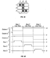
- Figures 4, 5A and 5B illustrate one possible actuation protocol for creating a display frame on the 3x3 array of Figure 2.
- Figure 4 illustrates a possible set of column and row voltage levels that may be used for pixels exhibiting the hysteresis curves of Figure 3.
- actuating a pixel involves setting the appropriate column to -V bias , and the appropriate row to + ⁇ V, which may correspond to -5 volts and +5 volts respectively Releasing the pixel is accomplished by setting the appropriate column to +V bias , and the appropriate row to the same + ⁇ V, producing a zero volt potential difference across the pixel. In those rows where the row voltage is held at zero volts, the pixels are stable in whatever state they were originally in, regardless of whether the column is at +V bias , or -V bias .
- Figure 5B is a timing diagram showing a series of row and column signals applied to the 3x3 array of Figure 2 which will result in the display arrangement illustrated in Figure 5A, where actuated pixels are non-reflective.
- the pixels Prior to writing the frame illustrated in Figure 5A, the pixels can be in any state, and in this example, all the rows are at 0 volts, and all the columns are at +5 volts. With these applied voltages, all pixels are stable in their existing actuated or released states.
- pixels (1,1), (1,2), (2,2), (3,2) and (3,3) are actuated.
- columns 1 and 2 are set to-5 volts, and column 3 is set to +5 volts. This does not change the state of any pixels, because all the pixels remain in the 3-7 volt stability window.
- Row 1 is then strobed with a pulse that goes from 0, up to 5 volts, and back to zero. This actuates the (1,1) and (1,2) pixels and releases the (1,3) pixel. No other pixels in the array are affected.
- column 2 is set to -5 volts
- columns 1 and 3 are set to +5 volts.
- Row 3 is similarly set by setting columns 2 and 3 to -5 volts, and column 1 to +5 volts.
- the row 3 strobe sets the row 3 pixels as shown in Figure 5A.. After writing the frame, the row potentials are zero, and the column potentials can remain at either +5 or -5 volts, and the display is then stable in the arrangement of Figure 5A. It will be appreciated that the same procedure can be employed for arrays of dozens or hundreds of rows and columns. It will also be appreciated that the timing, sequence, and levels of voltages used to perform row and column actuation can be varied widely within the general principles outlined above, and the above example is exemplary only, and any actuation voltage method can be used with the present invention.
- Figures 6A-6C illustrate three different embodiments of the moving mirror structure.
- Figure 6A is a cross section of the embodiment of Figure 1, where a strip of metal material 14 is deposited on orthogonally extending supports 18.
- the moveable reflective material 14 is attached to supports at the corners only, on tethers 32.
- the moveable reflective material 14 is suspended from a deformable layer 34.
- This embodiment has benefits because the structural design and materials used for the reflective material 14 can be optimized with respect to the optical properties, and the structural design and materials used for the deformable layer 34 can be optimized with respect to desired mechanical properties.
- a MEMS device such as an interferometric modulator array
- the moving parts of a MEMS device preferably have a protected space in which to move.
- Packaging techniques for a MEMS device will be described in more detail below.
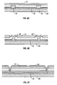
- a schematic of a basic package structure for a MEMS device, such as an interferometric modulator array, is illustrated in Figure 7.
- a basic package structure 70 includes a substrate 72 and a backplane cover or "cap" 74, wherein an interferometric modulator array 76 is formed on the substrate 72.
- This cap 74 is also called a "backplate".
- the substrate 72 and the backplane 74 are joined by a seal 78 to form the package structure 70, such that the interferometric modulator array 76 is encapsulated by the substrate 72, backplane 74, and the seal 78. This forms a cavity 79 between the backplane 74 and the substrate 72.
- the seal 78 may be a non-hermetic seal, such as a conventional epoxy-based adhesive.
- the seal 78 may be a polyisobutylene (sometimes called butyl rubber, and other times PIB), o-rings, polyurethane, thin film metal weld, liquid spin-on glass, solder, polymers, or plastics, among other types of seals that may have a range of permeability of water vapor of about 0.2 ⁇ 4.7 g mm/m 2 kPa day.
- the seal 78 may be a hermetic seal.
- the package structure 70 includes a desiccant 80 configured to reduce moisture within the cavity 79.
- a desiccant may not be necessary for a hermetically sealed package, but may be desirable to control moisture resident within the package.
- the desiccant 80 is positioned between the interferometric modulator array 76 and the backplane 74.
- Desiccants may be used for packages that have either hermetic or non-hermetic seals. In packages having a hermetic seal, desiccants are typically used to control moisture resident within the interior of the package. In packages having a non-hermetic seal, a desiccant may be used to control moisture moving into the package from the environment.
- any substance that can trap moisture while not interfering with the optical properties of the interferometric modulator array may be used as the desiccant 80.
- Suitable desiccant materials include, but are not limited to, zeolites, molecular sieves, surface adsorbents, bulk adsorbents, and chemical reactants.
- the desiccant 80 may be in different forms, shapes, and sizes. In addition to being in solid form, the desiccant 80 may alternatively be in powder form. These powders may be inserted directly into the package or they may be mixed with an adhesive for application. In an alternative embodiment, the desiccant 80 may be formed into different shapes, such as cylinders or sheets, before being applied inside the package.
- the desiccant 80 can be applied in different ways.
- the desiccant 80 is deposited as part of the interferometric modulator array 76.
- the desiccant 80 is applied inside the package 70 as a spray or a dip coat.
- the substrate 72 may be a semi-transparent or transparent substance capable of having thin film, MEMS devices built upon it. Such transparent substances include, but are not limited to, glass, plastic, and transparent polymers.
- the interferometric modulator array 76 may comprise membrane modulators or modulators of the separable type.
- the backplane 74 may be formed of any suitable material, such as glass, metal, foil, polymer, plastic, ceramic, or semiconductor materials (e.g., silicon).
- the packaging process may be accomplished in a vacuum, pressure between a vacuum up to and including ambient pressure, or pressure higher than ambient pressure.
- the packaging process may also be accomplished in an environment of varied and controlled high or low pressure during the sealing process.
- the packaging environment may be of an inert gas at ambient conditions. Packaging at ambient conditions allows for a lower cost process and more potential for versatility in equipment choice because the device may be transported through ambient conditions without affecting the operation of the device.
- a desiccant may be used to control moisture resident within the package structure 70.
- the need for a desiccant can be reduced or eliminated with the implementation of a hermetic seal 78 to prevent moisture from traveling from the atmosphere into the interior of the package structure 70.
- the continued reduction in display device dimensions restricts available methods to manage the environment within the package structure 70 because there is less area to place a desiccant 80 within the package structure 70.
- the elimination of the need for a desiccant also allows the package structure 70 to be thinner, which is desirable in some embodiments.
- the lifetime expectation of the packaged device may depend on the lifetime of the desiccant.
- the interferometric modulator device may fail as sufficient moisture thereafter enters the package structure and damages the interferometric modulator array.
- Embodiments of the invention relate to electronic displays for use in devices such as wireless telephones, personal digital assistants, digital music players, kid phones, and handheld video game players.
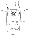
- Figure 8 illustrates a wireless telephone 100 with a display 102 according to one embodiment.
- the display 102 is configured to display images including text and graphics, such as telephone numbers, messages, time, date, video game characters and the like.
- the display 102 can be any type of display including light emitting diode (LED), organic light emitting diode (OLED), or an interferometric modulator (IMOD) direct view electronic display.
- the display 102 is configured to take advantage of an end-of-life phenomenon that occurs when a sufficient amount of water vapor is present in a packaging structure of the display so as to display an end-of-life image.
- the end-of life image can include, for example, a humorous message, a graphic image, a puzzle, or the like to signify that the device is no longer operable.
- the end-of-life phenomenon is preferably different for each device and is not revealed until triggered by one or more pre-determined conditions.
- a MEMS device when the humidity or water vapor within the package exceeds a level beyond which surface tension from the moisture becomes higher than the restoration force of movable elements (or layers, such as the movable layers 14a, 14b illustrated in Figure 1), the movable layers may become permanently adhered to the surface of an opposed fixed surface (fixed layers 16a, 16b of Figure 1) of a MEMS element.
- the presence of excessive water vapor in the MEMS device package enables the activated membranes to remain adhered to the thin film layer, as illustrated in Figure 1 by movable layer 14b and fixed layer 16b, without continued application of a voltage.
- a display pixel comprising a MEMS interferometric modulator will remain activated without application of a voltage in the presence of sufficient water vapor.
- the display device utilizes this aspect of a MEMS element to display a substantially permanent end-of-life image on the display.
- a display device comprises a MEMS interferometric modulator display configured for an end-of-life phenomenon that can be triggered by the presence of water vapor in excess of a predefined amount in the display packaging.
- a user of the display device activates the end-of-life phenomenon at any time during the lifetime of the display. This embodiment may be used, for example, as a novelty, wherein the device is intentionally contacted with water and the user then presses an activator button which permanently displays a humorous end-of-life message.
- the display device is configured to detect a predefined level of water vapor in the display package and display an end-of-life image in response to such detection.
- data representing a predetermined lifetime of the display device is stored in memory, and the device is configured to display an end-of-life image in response to determination of the expiration of the stored lifetime.
- preselected elements of the display comprise cavity heights smaller than unselected elements of the display, wherein an end-of-life image is displayed on the display according to the preselected elements when sufficient water vapor is present within the display device package.
- the packaging structure of the display device comprises a desiccant deposited on a backplane of the package structure, wherein a reduced amount or no desiccant is deposited in predefined areas.
- An end-of-life image is displayed on the device according to the display elements proximate the reduced desiccant areas of the package when sufficient water vapor is present in the device packaging structure.
- an end-of-life phenomenon is activated by the user.
- the user can contact the display with water vapor by, for example, placing it in a high humidity environment, such as adjacent to a pot of boiling water, to introduce water vapor into the display device packaging structure.
- the device reaches its end of life when the water absorption capacity-of the desiccant 80 ( Figure 8) has been exceeded, at which time the relative humidity inside the package increases, moving toward equilibrium with the external environment.
- the water vapor can either enter through the seal 78 of the packaging structure 70 in the case of a semi-hermetic package, or the packaging structure 70 may include an aperture with a plug 108 as shown in Figure 8, wherein the user removes the plug 108 to intentionally contact the display device with water vapor.
- a user can breathe into the packaging structure to contact the display with water vapor.
- the user can then activate the display via an "end-of-life" switch 106, for example, wherein the display device is configured to display a predefined image 104 on the display in response to such user activation.
- the display device may be configured to apply a predefined voltage to the display in response to user activation of the switch 106.
- the movable layers of selected MEMS elements are moved into contact with their respective fixed layer to display the end-of-life image.
- the excessive moisture in the display causes the movable layers to become permanently adhered to the fixed layers, such that the image remains on the display without continued activation of the display.
- the user activates the display for display of the end-of-life image 104 by depressing a predefined combination of keys, buttons, or switches 110 on the device.
- a user can, for example, cause a novelty display to be permanently active.
- the MEMS display device includes a water vapor reservoir within the packaging structure, wherein the reservoir can be activated by the user to release water vapor in the packaging structure and in contact with the MEMS display.
- the MEMS display device includes a desiccant holding water or water vapor, wherein the user can release the water or water vapor from the desiccant by applying heat to the desiccant. Heat can be applied to the desiccant, for example, with a heated or hot-tipped stylus.
- the predefined end-of-life image 104 may be prestored by the display device manufacturer, distributor, or retailer, for example, and/or the device may be configured for selection or programming of the end-of-life image by the user.
- the end-of-life image is customized by the user to include a selected image including at least one of text and graphics.
- the end-of-life image may include text corresponding to the user's name, such as "GOOD-BYE LAUREN".
- the device may include a default end-of-life message which is displayed in the absence of a user selected image or in addition to the image selected by the user.
- a display device in another embodiment, includes a water vapor sensor within the display packaging structure, as illustrated in Figures 9A-B.
- Figure 9A is a block diagram of one embodiment of a display device with a water vapor sensor 904, wherein the water vapor sensor 904 is coupled to a sensor circuit 906, which is coupled to a processor 908.
- the water vapor sensor 904 may be any sensor known in the art. An exemplary water vapor sensor is discussed in more detail in reference to Figure 9B.
- the processor 908 may be any general purpose single- or multi-chip microprocessor such as an ARM, Pentium®, Pentium II® , Pentium III® , Pentium IV® , Pentium® Pro, an 8051, a MIPS® , a Power PC® , an ALPHA® , or any special purpose microprocessor such as a digital signal processor, microcontroller, or a programmable gate array.
- the processor 908 may be configured to execute one or more software modules.
- the processor may be configured to execute one or more software applications, including a web browser, a telephone application, an email program, or any other software application.
- the water vapor sensor 904 is configured to detect the presence of water vapor in the display device package structure in excess of a predefined level in combination with the sensor circuit 906.
- the sensor circuit 906 is configured to transmit a detection signal to the processor 908 in response to detection of water vapor at the water vapor sensor 904 above a predefined level.
- the water vapor sensor 904 is configured to detect a specific amount of water vapor in addition to the presence of water vapor of a predefined level, such that the water vapor sensor 904 and sensor circuit 906 are configured to determine whether water vapor in the display device packaging structure is above a plurality of predefined levels. Accordingly, the sensor circuit 906 is configured to transmit an appropriate detection signal to the processor 908 corresponding to the level of water vapor sensed in the display device packaging structure.
- the processor 908 is also configured to communicate with an array controller 910.
- the array controller 910 includes a row driver circuit 912 and a column driver circuit 914 that provide signals to a pixel array 916 of a MEMS display.
- the processor is configured to activate the pixel array 916 to display an end-of-life image by transmitting an appropriate signal to the array controller 910. Activated pixels of the array 916 will remain in the active state without continued activation via the array controller 910 in the presence of sufficient water vapor as detected by the water vapor sensor 904, and the end-of-life image will remain substantially permanent.
- the processor 908 is further configured to store information input by the user in memory, such as a flash memory or a programmable read only memory (PROM), in response to a detection signal from the sensor circuit 906.
- memory such as a flash memory or a programmable read only memory (PROM)
- the processor may be configured to store the telephone numbers previously input by the user in a flash memory or EEPROM.
- the end-of-life image may include a message indicating that the user's information has been stored.
- the device may be configured to display a different image depending on the predefined level of water vapor that is exceeded.
- the display device may be configured to display a first image when a first predefined level of water vapor is exceeded, such as "THE LIFE OF YOUR DISPLAY WILL END IN 3 DAYS: TIME TO BUY A NEW PHONE", a second image when a second predefined level of water vapor is exceeded, such as "THE LIFE OF YOUR DISPLAY WILL END IN 1 DAY", and a third, end-of-life image when a third predefined level of water vapor is exceeded.
- the processor 908 may be configured to facilitate display of a user prompt to store information in response to receipt of a detection signal from the sensor circuit 906, such as "Your Display is going to die in 3 days: store numbers?"
- the display device may be configured to send and receive messages or images in response to detection of a predefined level of water vapor in the display device package structure.
- the display device may be configured to display advertising messages from a manufacturer with regard to prices of new devices in response to detection of a predefined level of water vapor.
- the device in response to detection of a predefined level of water vapor, the device may be configured to notify a device manufacturer or service provider which sends an advertisement with respect to devices for sale in response to the notification.
- the display device is further configured to display the advertisement received from the manufacturer or service provider to the user.
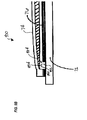
- Figure 9B is a partial cross section view of a display device packaging structure with an exemplary water vapor sensor 904.
- the water vapor sensor 904 illustrated in Figure 9B comprises two conductive members 950, 952 with an air gap 954 between the conductive members 950, 952.
- the resistance between the conductive members 950, 952 is substantially infinite.
- the sensor circuit 906 may be outside the enclosed packaging structure or within the packaging structure.
- the water vapor sensor described is exemplary in nature and other sensors are within the scope of the invention.
- the operational lifetime of the display is predetermined according to properties of the device and packaging.
- the operational lifetime of the display may be determined based on the maximum water vapor presence at which the movable layer of a MEMS element will still be separable from its corresponding fixed layer without continued activation.
- the operational lifetime of the display may be determined based at least in part on the absorption capacity of a desiccant included in the display packaging structure and expected permeation rate of water vapor into the packaging structure.
- data representing the operational lifetime of a display is stored in a memory coupled to a processor, such as the processor 21 of Figure 2, wherein the processor is configured to determine when the predetermined lifetime has expired.
- the processor In response to determining the expiration of the display's lifetime, the processor is configured to coordinate activation of the display such that a predefined image is displayed to the user. In one embodiment, the processor is further configured to determine when the current life of the MEMS display is within a predefined range of the predetermined lifetime, and coordinate activation of the display so as to display a warning image in response to determining that the current life the MEMS display is within the predefined range of the predetermined lifetime.
- individual MEMS elements of the MEMS display have differing cavity heights.
- the depicted portion of the MEMS array in Figure 10 includes five adjacent MEMS elements 1002a-e.
- the MEMS elements 1002a-e comprise a mechanical or movable layer 1004 and an electrically conductive fixed layer 1006, wherein the movable layer 1004 is positioned on top of posts 1008a-f and the conductive fixed layer 1006 is formed on a substrate 1009.
- the movable layer 1004 and fixed layer 1006 form cavities 1010a-e for each respective MEMS element 1002a-e.
- the posts 1008a-f have differing heights, and thereby the respective cavities 1010a-e for each MEMS element 1002a-e have a different height.
- the mechanical or movable layer 1004 will remain adhered to the fixed layer 1006 in the presence of less water vapor than the MEMS elements 1002a, e with a greater cavity height.
- an image will be displayed on the MEMS display according to the MEMS elements with a reduced cavity height in the presence of sufficient water vapor.
- the display device packaging structure includes a desiccant with varied degrees of absorbent capacity across its surface.
- Figure 11 is a cross section view of one exemplary implementation of a display device package structure with a varied desiccant 80. Elements similar to those illustrated in Figure 7 and described in reference thereto are labeled with corresponding reference numerals. As illustrated in Figure 11, the desiccant 80 is applied to the backplane 74 of the packaging structure, wherein the desiccant 80 includes preselected areas 1102 having substantially less desiccant 80 than other unselected areas.
- the MEMS elements of the display device 76 located proximate to the preselected areas 1102 will remain in a permanently active state, wherein the movable layer adheres to the fixed layer, in the presence of sufficient water vapor in the packaging structure due to the reduced desiccant 80, whereas the MEMS elements proximate the unselected areas of the desiccant 80 will remain operational because the desiccant 80 has retained the water vapor in those areas. Accordingly, a predefined image will be displayed on the MEMS display device 76 according to the MEMS elements in the preselected areas 1102.
- the preselected areas of the desiccant may include no desiccant, or desiccant with a reduced absorption capacity in comparison to the desiccant in the unselected areas.
- a user can apply a temperature differential to a surface of the display package, such as extreme cold or heat, thereby causing movement of water vapor molecules in the display device packaging structure proximate areas where the temperature differential is applied.
- the temperature differential can be applied, for example, with a cold or hot tipped stylus to the surface of the display, wherein an image is displayed according to the areas where the stylus is applied.
- the generated effect is similar to that of novelty devices wherein a magnetic stylus is applied to a surface of a screen containing metallic filaments, such that the metallic filaments are attracted to the surface of the screen according to the application of the magnetic stylus to display an image.
- a hot-tipped stylus is used, the MEMS elements that are contacted are released to a reflective or white state, and when a cold-tipped stylus is used, the MEMS elements that are contacted are stuck in an activated or black state.
- FIG. 12A is an exemplary illustration of a MEMS display 1200 comprising a plurality of MEMS elements 1202, wherein a reduced temperature has been applied to selective areas 1204.
- Application of the reduced temperature generates condensation of water vapor molecules present in the MEMS display device package at the selective areas 1204 where the reduced temperature is applied.
- the amount of water vapor present in the MEMS display device package is sufficient to further actuate or maintain MEMS elements in an activated position at the selected areas, such that an image is displayed at the selected areas 1204 as illustrated in Figure 12A.
- the method may further comprise activating the display to actuate the movable layers of a plurality of MEMS elements, and then de-activating the display to move the movable layers of a plurality of MEMS elements to a released state. Due to the condensation of water vapor molecules at the selected areas 1204, the MEMS elements in the selected areas 1204 will remain in an actuated position without continued activation, thereby displaying an image on the MEMS display at the selected areas, as illustrated in Figure 12A for example. In some embodiments, the display may be further activated to clear the display of the image.
- FIG. 12B is an exemplary illustration of a MEMS display 1220 comprising a plurality of MEMS elements 1222, wherein an increased temperature has been applied to selective areas 1224 of the display which has reached the end of its operational lifetime.
- the MEMS display device has already reached the end of its operational lifetime due to the presence of sufficient water vapor in the MEMS display device package, wherein a plurality of the MEMS elements of the display remain in an activated or actuated state without continued activation.
- substantially all of the MEMS elements are in an activated state without continued activation, as illustrated in Figure 12B.
- the MEMS elements at the selected areas 1224 move to a released state as the water vapor retaining the movable membrane in the activated state evaporates in response to the increased temperature application.
- the MEMS elements at the selected areas 1224 are in a released state while MEMS elements in unselected areas remain in an activated state, thereby displaying an image according to the selected areas 1224.
- the method may include detecting a predefined level of water vapor within the MEMS display device package and notifying a user that the display is near the end of its operable lifetime. The user may then apply the reduced temperature to display an image at selected areas of the display as discussed above. Alternatively, in response to notification that the display is near the end of its operable lifetime, the user may activate the display when sufficient water vapor is present in the display package such that a plurality of MEMS elements remain in an activated position without continued activation. The user may then apply an increased temperature to selective areas of the display such that the MEMS elements at the selected areas are "released" to a released state, thereby displaying an image on the display according to the selected areas. In additional embodiments, a user may intentionally contact the MEMS display with water vapor as discussed above with respect to other embodiments of the invention. In addition, the method may further comprise activation of the display to clear the image.
- a MEMS display device has a significant tolerance for water vapor, wherein the display will continue to operate in the presence of a significant level of water vapor as compared to other display devices such as OLED's. It is generally known that OLED displays have significant environmental constraints on the amount of water and oxygen present both during assembly and inside the final package display. In contrast, embodiments of MEMS displays do not mandate an inert, vacuum or dry environment during assembly or operation. Thus, MEMS displays tolerate exposure to significant levels of water vapor before reaching a non-operational state, whereas an OLED display device has substantially zero tolerance for the presence of water vapor and the entirety of an OLED display will be non-operational once exposed to a small level of water vapor. The ability of MEMS display elements to tolerate the presence of water vapor and remain operational allows for the implementation of the above-described embodiments of display devices with end-of-life phenomena.
- FIGS 13A and 13B are system block diagrams illustrating an embodiment of a display device 2040.
- the display device 2040 can be, for example, a cellular or mobile telephone.
- the same components of display device 2040 or slight variations thereof are also illustrative of various types of display devices such as televisions and portable media players.
- the display device 2040 includes a housing 2041, a display 2030, an antenna 2043, a speaker 2045, an input device 2048, and a microphone 2046.
- the housing 2041 is generally formed from any of a variety of manufacturing processes as are well known to those of skill in the art, including injection molding, and vacuum forming.
- the housing 2041 may be made from any of a variety of materials, including but not limited to plastic, metal, glass, rubber, and ceramic, or a combination thereof.
- the housing 2041 includes removable portions (not shown) that may be interchanged with other removable portions of different color, or containing different logos, pictures, or symbols.
- the display 2030 of exemplary display device 2040 may be any of a variety of displays, including a bi-stable display, as described herein.
- the display 2030 includes a flat-panel display, such as plasma, EL, OLED, STN LCD, or TFT LCD as described above, or a non-flat-panel display, such as a CRT or other tube device, as is well known to those of skill in the art.
- the display 2030 includes an interferometric modulator display, as described herein.
- the components of one embodiment of exemplary display device 2040 are schematically illustrated in Figure 13B.
- the illustrated exemplary display device 2040 includes a housing 2041 and can include additional components at least partially enclosed therein.
- the exemplary display device 2040 includes a network interface 2027 that includes an antenna 2043 which is coupled to a transceiver 2047.
- the transceiver 2047 is connected to the processor 2021, which is connected to conditioning hardware 2052.
- the conditioning hardware 2052 may be configured to condition a signal (e.g. filter a signal).
- the conditioning hardware 2052 is connected to a speaker 2045 and a microphone 2046.
- the processor 2021 is also connected to an input device 2048 and a driver controller 2029.
- the driver controller 2029 is coupled to a frame buffer 2028 and to the array driver 2022, which in turn is coupled to a display array 2030.
- a power supply 2050 provides power to all components as required by the particular exemplary display device 2040 design.
- the network interface 2027 includes the antenna 2043 and the transceiver 2047 so that the exemplary display device 2040 can communicate with one or more devices over a network. In one embodiment the network interface 2027 may also have some processing capabilities to relieve requirements of the processor 2021.
- the antenna 2043 is any antenna known to those of skill in the art for transmitting and receiving signals. In one embodiment, the antenna transmits and receives RF signals according to the IEEE 802.11 standard, including IEEE 802.11(a), (b), or (g). In another embodiment, the antenna transmits and receives RF signals according to the BLUETOOTH standard. In the case of a cellular telephone, the antenna is designed to receive CDMA, GSM, AMPS or other known signals that are used to communicate within a wireless cell phone network.
- the transceiver 2047 pre-processes the signals received from the antenna 2043 so that they may be received by and further manipulated by the processor 2021.
- the transceiver 2047 also processes signals received from the processor 2021 so that they may be transmitted from the exemplary display device 2040 via the antenna 2043.
- the transceiver 2047 can be replaced by a receiver.
- network interface 2027 can be replaced by an image source, which can store or generate image data to be sent to the processor 2021.
- the image source can be a digital video disc (DVD) or a hard-disc drive that contains image data, or a software module that generates image data.
- Processor 2021 generally controls the overall operation of the exemplary display device 2040.
- the processor 2021 receives data, such as compressed image data from the network interface 2027 or an image source, and processes the data into raw image data or into a format that is readily processed into raw image data.
- the processor 2021 then sends the processed data to the driver controller 2029 or to frame buffer 2028 for storage.
- Raw data typically refers to the information that identifies the image characteristics at each location within an image. For example, such image characteristics can include color, saturation, and gray-scale level.
- the processor 2021 includes a microcontroller, CPU, or logic unit to control operation of the exemplary display device 2040.
- Conditioning hardware 2052 generally includes amplifiers and filters for transmitting signals to the speaker 2045, and for receiving signals from the microphone 2046.
- Conditioning hardware 2052 may be discrete components within the exemplary display device 2040, or may be incorporated within the processor 2021 or other components.
- the driver controller 2029 takes the raw image data generated by the processor 2021 either directly from the processor 2021 or from the frame buffer 2028 and reformats the raw image data appropriately for high speed transmission to the array driver 2022. Specifically, the driver controller 2029 reformats the raw image data into a data flow having a raster-like format, such that it has a time order suitable for scanning across the display array 2030. Then the driver controller 2029 sends the formatted information to the array driver 2022.
- a driver controller 2029 such as a LCD controller, is often associated with the system processor 2021 as a stand-alone Integrated Circuit (IC), such controllers may be implemented in many ways. They may be embedded in the processor 2021 as hardware, embedded in the processor 2021 as software, or fully integrated in hardware with the array driver 2022.
- IC Integrated Circuit
- the array driver 2022 receives the formatted information from the driver controller 2029 and reformats the video data into a parallel set of waveforms that are applied many times per second to the hundreds and sometimes thousands of leads coming from the display's x-y matrix of pixels.
- driver controller 2029, array driver 2022, and display array 2030 are appropriate for any of the types of displays described herein.
- driver controller 2029 is a conventional display controller or a bi-stable display controller (e.g., an interferometric modulator controller).
- array driver 2022 is a conventional driver or a bi-stable display driver (e.g., an interferometric modulator display).
- a driver controller 2029 is integrated with the array driver 2022.
- display array 2030 is a typical display array or a bi-stable display array (e.g., a display including an array of interferometric modulators).
- the input device 2048 allows a user to control the operation of the exemplary display device 2040.
- input device 2048 includes a keypad, such as a QWERTY keyboard or a telephone keypad, a button, a switch, a touch-sensitive screen, a pressure- or heat-sensitive membrane.
- the microphone 2046 is an input device for the exemplary display device 2040. When the microphone 2046 is used to input data to the device, voice commands may be provided by a user for controlling operations of the exemplary display device 2040.
- Power supply 2050 can include a variety of energy storage devices as are well known in the art.
- power supply 2050 is a rechargeable battery, such as a nickel-cadmium battery or a lithium ion battery.
- power supply 2050 is a renewable energy source, a capacitor, or a solar cell, including a plastic solar cell, and solar-cell paint.
- power supply 2050 is configured to receive power from a wall outlet.
- control programmability resides, as described above, in a driver controller which can be located in several places in the electronic display system. In some cases control programmability resides in the array driver 2022. Those of skill in the art will recognize that the above-described optimization may be implemented in any number of hardware and/or software components and in various configurations.
Applications Claiming Priority (2)
| Application Number | Priority Date | Filing Date | Title |
|---|---|---|---|
| US61348504P | 2004-09-27 | 2004-09-27 | |
| US11/102,543 US7916103B2 (en) | 2004-09-27 | 2005-04-08 | System and method for display device with end-of-life phenomena |
Publications (2)
| Publication Number | Publication Date |
|---|---|
| EP1640332A2 true EP1640332A2 (fr) | 2006-03-29 |
| EP1640332A3 EP1640332A3 (fr) | 2008-09-10 |
Family
ID=35462241
Family Applications (1)
| Application Number | Title | Priority Date | Filing Date |
|---|---|---|---|
| EP05255707A Withdrawn EP1640332A3 (fr) | 2004-09-27 | 2005-09-14 | Système et procédé pour dispositif d'affichage avec effet de fin de vie |
Country Status (10)
| Country | Link |
|---|---|
| US (2) | US7916103B2 (fr) |
| EP (1) | EP1640332A3 (fr) |
| JP (1) | JP2006099107A (fr) |
| KR (2) | KR101174759B1 (fr) |
| AU (1) | AU2005211623A1 (fr) |
| BR (1) | BRPI0503848A (fr) |
| CA (1) | CA2520950A1 (fr) |
| RU (1) | RU2005129846A (fr) |
| SG (1) | SG121163A1 (fr) |
| TW (1) | TW200624370A (fr) |
Cited By (5)
| Publication number | Priority date | Publication date | Assignee | Title |
|---|---|---|---|---|
| WO2009123836A1 (fr) * | 2008-03-31 | 2009-10-08 | Qualcomm Mems Technologies, Inc. | Capteurs environnementaux à deux états, lisibles par l'homme, à base de membranes mécaniques |
| WO2009137162A2 (fr) * | 2008-03-31 | 2009-11-12 | Qualcomm Mems Technologies, Inc. | Capteurs de variables d'environnement à deux états, lisibles par un être humain, à base de membranes mécaniques |
| US7787171B2 (en) | 2008-03-31 | 2010-08-31 | Qualcomm Mems Technologies, Inc. | Human-readable, bi-state environmental sensors based on micro-mechanical membranes |
| US8077326B1 (en) | 2008-03-31 | 2011-12-13 | Qualcomm Mems Technologies, Inc. | Human-readable, bi-state environmental sensors based on micro-mechanical membranes |
| WO2012027340A1 (fr) * | 2010-08-26 | 2012-03-01 | Qualcomm Mems Technologies, Inc. | Système et procédé pour déterminer l'humidité à partir de la détermination d'un écart de tension de décalage |
Families Citing this family (13)
| Publication number | Priority date | Publication date | Assignee | Title |
|---|---|---|---|---|
| US7126569B2 (en) * | 1999-03-23 | 2006-10-24 | Minolta Co., Ltd. | Liquid crystal display device |
| TWI289708B (en) | 2002-12-25 | 2007-11-11 | Qualcomm Mems Technologies Inc | Optical interference type color display |
| US7342705B2 (en) | 2004-02-03 | 2008-03-11 | Idc, Llc | Spatial light modulator with integrated optical compensation structure |
| US7916103B2 (en) * | 2004-09-27 | 2011-03-29 | Qualcomm Mems Technologies, Inc. | System and method for display device with end-of-life phenomena |
| US7405924B2 (en) * | 2004-09-27 | 2008-07-29 | Idc, Llc | System and method for protecting microelectromechanical systems array using structurally reinforced back-plate |
| EP1979268A2 (fr) | 2006-04-13 | 2008-10-15 | Qualcomm Mems Technologies, Inc. | Encapsulation d'un dispositif mems à l'aide d'un cadre |
| US8872085B2 (en) | 2006-10-06 | 2014-10-28 | Qualcomm Mems Technologies, Inc. | Display device having front illuminator with turning features |
| KR20150014978A (ko) | 2006-10-06 | 2015-02-09 | 퀄컴 엠이엠에스 테크놀로지스, 인크. | 디스플레이 장치 및 디스플레이의 형성 방법 |
| US8068710B2 (en) * | 2007-12-07 | 2011-11-29 | Qualcomm Mems Technologies, Inc. | Decoupled holographic film and diffuser |
| US20090323170A1 (en) * | 2008-06-30 | 2009-12-31 | Qualcomm Mems Technologies, Inc. | Groove on cover plate or substrate |
| US8379392B2 (en) * | 2009-10-23 | 2013-02-19 | Qualcomm Mems Technologies, Inc. | Light-based sealing and device packaging |
| US8711361B2 (en) * | 2009-11-05 | 2014-04-29 | Qualcomm, Incorporated | Methods and devices for detecting and measuring environmental conditions in high performance device packages |
| CN113437242B (zh) * | 2021-06-29 | 2023-06-20 | 固安翌光科技有限公司 | 一种封装结构以及光电器件 |
Citations (3)
| Publication number | Priority date | Publication date | Assignee | Title |
|---|---|---|---|---|
| EP0980014A1 (fr) | 1998-06-02 | 2000-02-16 | Texas Instruments Incorporated | Dispositif microméchanique au ressort annulaire |
| US20020015215A1 (en) | 1994-05-05 | 2002-02-07 | Iridigm Display Corporation, A Delaware Corporation | Interferometric modulation of radiation |
| US20020024711A1 (en) | 1994-05-05 | 2002-02-28 | Iridigm Display Corporation, A Delaware Corporation | Interferometric modulation of radiation |
Family Cites Families (231)
| Publication number | Priority date | Publication date | Assignee | Title |
|---|---|---|---|---|
| US2534846A (en) | 1946-06-20 | 1950-12-19 | Emi Ltd | Color filter |
| DE1288651B (de) * | 1963-06-28 | 1969-02-06 | Siemens Ag | Anordnung elektrischer Dipole fuer Wellenlaengen unterhalb 1 mm und Verfahren zur Herstellung einer derartigen Anordnung |
| FR1603131A (fr) * | 1968-07-05 | 1971-03-22 | ||
| US3653741A (en) * | 1970-02-16 | 1972-04-04 | Alvin M Marks | Electro-optical dipolar material |
| US3813265A (en) * | 1970-02-16 | 1974-05-28 | A Marks | Electro-optical dipolar material |
| DE2336930A1 (de) * | 1973-07-20 | 1975-02-06 | Battelle Institut E V | Infrarot-modulator (ii.) |
| US4036360A (en) * | 1975-11-12 | 1977-07-19 | Graham Magnetics Incorporated | Package having dessicant composition |
| US4034609A (en) * | 1976-01-02 | 1977-07-12 | Fuller David L | Digital sensing device |
| US4074480A (en) * | 1976-02-12 | 1978-02-21 | Burton Henry W G | Kit for converting single-glazed window to double-glazed window |
| US4099854A (en) * | 1976-10-12 | 1978-07-11 | The Unites States Of America As Represented By The Secretary Of The Navy | Optical notch filter utilizing electric dipole resonance absorption |
| US4389096A (en) * | 1977-12-27 | 1983-06-21 | Matsushita Electric Industrial Co., Ltd. | Image display apparatus of liquid crystal valve projection type |
| US4445050A (en) * | 1981-12-15 | 1984-04-24 | Marks Alvin M | Device for conversion of light power to electric power |
| US4663083A (en) | 1978-05-26 | 1987-05-05 | Marks Alvin M | Electro-optical dipole suspension with reflective-absorptive-transmissive characteristics |
| US4431691A (en) * | 1979-01-29 | 1984-02-14 | Tremco, Incorporated | Dimensionally stable sealant and spacer strip and composite structures comprising the same |
| US4228437A (en) | 1979-06-26 | 1980-10-14 | The United States Of America As Represented By The Secretary Of The Navy | Wideband polarization-transforming electromagnetic mirror |
| NL8001281A (nl) * | 1980-03-04 | 1981-10-01 | Philips Nv | Weergeefinrichting. |
| US4377324A (en) * | 1980-08-04 | 1983-03-22 | Honeywell Inc. | Graded index Fabry-Perot optical filter device |
| US4441791A (en) * | 1980-09-02 | 1984-04-10 | Texas Instruments Incorporated | Deformable mirror light modulator |
| FR2506026A1 (fr) | 1981-05-18 | 1982-11-19 | Radant Etudes | Procede et dispositif pour l'analyse d'un faisceau de rayonnement d'ondes electromagnetiques hyperfrequence |
| NL8103377A (nl) | 1981-07-16 | 1983-02-16 | Philips Nv | Weergeefinrichting. |
| US4571603A (en) | 1981-11-03 | 1986-02-18 | Texas Instruments Incorporated | Deformable mirror electrostatic printer |
| NL8200354A (nl) * | 1982-02-01 | 1983-09-01 | Philips Nv | Passieve weergeefinrichting. |
| US4500171A (en) * | 1982-06-02 | 1985-02-19 | Texas Instruments Incorporated | Process for plastic LCD fill hole sealing |
| US4482213A (en) | 1982-11-23 | 1984-11-13 | Texas Instruments Incorporated | Perimeter seal reinforcement holes for plastic LCDs |
| US4566935A (en) | 1984-07-31 | 1986-01-28 | Texas Instruments Incorporated | Spatial light modulator and method |
| US4710732A (en) | 1984-07-31 | 1987-12-01 | Texas Instruments Incorporated | Spatial light modulator and method |
| US4596992A (en) | 1984-08-31 | 1986-06-24 | Texas Instruments Incorporated | Linear spatial light modulator and printer |
| US4662746A (en) | 1985-10-30 | 1987-05-05 | Texas Instruments Incorporated | Spatial light modulator and method |
| US5096279A (en) * | 1984-08-31 | 1992-03-17 | Texas Instruments Incorporated | Spatial light modulator and method |
| US5061049A (en) | 1984-08-31 | 1991-10-29 | Texas Instruments Incorporated | Spatial light modulator and method |
| US4615595A (en) | 1984-10-10 | 1986-10-07 | Texas Instruments Incorporated | Frame addressed spatial light modulator |
| US5172262A (en) | 1985-10-30 | 1992-12-15 | Texas Instruments Incorporated | Spatial light modulator and method |
| US5835255A (en) | 1986-04-23 | 1998-11-10 | Etalon, Inc. | Visible spectrum modulator arrays |
| GB8610129D0 (en) | 1986-04-25 | 1986-05-29 | Secr Defence | Electro-optical device |
| US4748366A (en) | 1986-09-02 | 1988-05-31 | Taylor George W | Novel uses of piezoelectric materials for creating optical effects |
| US4786128A (en) | 1986-12-02 | 1988-11-22 | Quantum Diagnostics, Ltd. | Device for modulating and reflecting electromagnetic radiation employing electro-optic layer having a variable index of refraction |
| US4977009A (en) | 1987-12-16 | 1990-12-11 | Ford Motor Company | Composite polymer/desiccant coatings for IC encapsulation |
| US4956619A (en) | 1988-02-19 | 1990-09-11 | Texas Instruments Incorporated | Spatial light modulator |
| US4856863A (en) * | 1988-06-22 | 1989-08-15 | Texas Instruments Incorporated | Optical fiber interconnection network including spatial light modulator |
| US5028939A (en) * | 1988-08-23 | 1991-07-02 | Texas Instruments Incorporated | Spatial light modulator system |
| US4982184A (en) | 1989-01-03 | 1991-01-01 | General Electric Company | Electrocrystallochromic display and element |
| US5287096A (en) | 1989-02-27 | 1994-02-15 | Texas Instruments Incorporated | Variable luminosity display system |
| US5446479A (en) * | 1989-02-27 | 1995-08-29 | Texas Instruments Incorporated | Multi-dimensional array video processor system |
| US5214420A (en) * | 1989-02-27 | 1993-05-25 | Texas Instruments Incorporated | Spatial light modulator projection system with random polarity light |
| US5162787A (en) | 1989-02-27 | 1992-11-10 | Texas Instruments Incorporated | Apparatus and method for digitized video system utilizing a moving display surface |
| KR100202246B1 (ko) | 1989-02-27 | 1999-06-15 | 윌리엄 비. 켐플러 | 디지탈화 비디오 시스템을 위한 장치 및 방법 |
| US5272473A (en) | 1989-02-27 | 1993-12-21 | Texas Instruments Incorporated | Reduced-speckle display system |
| US5206629A (en) * | 1989-02-27 | 1993-04-27 | Texas Instruments Incorporated | Spatial light modulator and memory for digitized video display |
| US5192946A (en) | 1989-02-27 | 1993-03-09 | Texas Instruments Incorporated | Digitized color video display system |
| US5079544A (en) * | 1989-02-27 | 1992-01-07 | Texas Instruments Incorporated | Standard independent digitized video system |
| US5214419A (en) * | 1989-02-27 | 1993-05-25 | Texas Instruments Incorporated | Planarized true three dimensional display |
| US5170156A (en) | 1989-02-27 | 1992-12-08 | Texas Instruments Incorporated | Multi-frequency two dimensional display system |
| US5022745A (en) * | 1989-09-07 | 1991-06-11 | Massachusetts Institute Of Technology | Electrostatically deformable single crystal dielectrically coated mirror |
| US4954789A (en) | 1989-09-28 | 1990-09-04 | Texas Instruments Incorporated | Spatial light modulator |
| US5381253A (en) * | 1991-11-14 | 1995-01-10 | Board Of Regents Of University Of Colorado | Chiral smectic liquid crystal optical modulators having variable retardation |
| US5124834A (en) * | 1989-11-16 | 1992-06-23 | General Electric Company | Transferrable, self-supporting pellicle for elastomer light valve displays and method for making the same |
| US5037173A (en) * | 1989-11-22 | 1991-08-06 | Texas Instruments Incorporated | Optical interconnection network |
| US5500635A (en) | 1990-02-20 | 1996-03-19 | Mott; Jonathan C. | Products incorporating piezoelectric material |
| CH682523A5 (fr) * | 1990-04-20 | 1993-09-30 | Suisse Electronique Microtech | Dispositif de modulation de lumière à adressage matriciel. |
| GB9012099D0 (en) | 1990-05-31 | 1990-07-18 | Kodak Ltd | Optical article for multicolour imaging |
| US5216537A (en) * | 1990-06-29 | 1993-06-01 | Texas Instruments Incorporated | Architecture and process for integrating DMD with control circuit substrates |
| US5083857A (en) * | 1990-06-29 | 1992-01-28 | Texas Instruments Incorporated | Multi-level deformable mirror device |
| US5099353A (en) * | 1990-06-29 | 1992-03-24 | Texas Instruments Incorporated | Architecture and process for integrating DMD with control circuit substrates |
| EP0467048B1 (fr) * | 1990-06-29 | 1995-09-20 | Texas Instruments Incorporated | Dispositif à mirroir déformable avec mise à jour de trame |
| US5142405A (en) | 1990-06-29 | 1992-08-25 | Texas Instruments Incorporated | Bistable dmd addressing circuit and method |
| US5018256A (en) * | 1990-06-29 | 1991-05-28 | Texas Instruments Incorporated | Architecture and process for integrating DMD with control circuit substrates |
| US5304419A (en) | 1990-07-06 | 1994-04-19 | Alpha Fry Ltd | Moisture and particle getter for enclosures |
| US5153771A (en) | 1990-07-18 | 1992-10-06 | Northrop Corporation | Coherent light modulation and detector |
| US5526688A (en) * | 1990-10-12 | 1996-06-18 | Texas Instruments Incorporated | Digital flexure beam accelerometer and method |
| US5192395A (en) | 1990-10-12 | 1993-03-09 | Texas Instruments Incorporated | Method of making a digital flexure beam accelerometer |
| US5044736A (en) | 1990-11-06 | 1991-09-03 | Motorola, Inc. | Configurable optical filter or display |
| US5331454A (en) * | 1990-11-13 | 1994-07-19 | Texas Instruments Incorporated | Low reset voltage process for DMD |
| US5602671A (en) | 1990-11-13 | 1997-02-11 | Texas Instruments Incorporated | Low surface energy passivation layer for micromechanical devices |
| US5233459A (en) * | 1991-03-06 | 1993-08-03 | Massachusetts Institute Of Technology | Electric display device |
| CA2063744C (fr) | 1991-04-01 | 2002-10-08 | Paul M. Urbanus | Architecture et dispositif de synchronisation de systeme d'affichage a modulation d'impulsions en duree |
| US5142414A (en) | 1991-04-22 | 1992-08-25 | Koehler Dale R | Electrically actuatable temporal tristimulus-color device |
| US5226099A (en) | 1991-04-26 | 1993-07-06 | Texas Instruments Incorporated | Digital micromirror shutter device |
| US5179274A (en) | 1991-07-12 | 1993-01-12 | Texas Instruments Incorporated | Method for controlling operation of optical systems and devices |
| US5168406A (en) | 1991-07-31 | 1992-12-01 | Texas Instruments Incorporated | Color deformable mirror device and method for manufacture |
| US5254980A (en) | 1991-09-06 | 1993-10-19 | Texas Instruments Incorporated | DMD display system controller |
| US5563398A (en) | 1991-10-31 | 1996-10-08 | Texas Instruments Incorporated | Spatial light modulator scanning system |
| CA2081753C (fr) | 1991-11-22 | 2002-08-06 | Jeffrey B. Sampsell | Dispositif de balayage a miroir deformable |
| US5233385A (en) | 1991-12-18 | 1993-08-03 | Texas Instruments Incorporated | White light enhanced color field sequential projection |
| US5233456A (en) | 1991-12-20 | 1993-08-03 | Texas Instruments Incorporated | Resonant mirror and method of manufacture |
| US5244707A (en) | 1992-01-10 | 1993-09-14 | Shores A Andrew | Enclosure for electronic devices |
| CA2087625C (fr) * | 1992-01-23 | 2006-12-12 | William E. Nelson | Retard non systolique et impression integree |
| US5296950A (en) | 1992-01-31 | 1994-03-22 | Texas Instruments Incorporated | Optical signal free-space conversion board |
| US5231532A (en) | 1992-02-05 | 1993-07-27 | Texas Instruments Incorporated | Switchable resonant filter for optical radiation |
| DE69310974T2 (de) * | 1992-03-25 | 1997-11-06 | Texas Instruments Inc | Eingebautes optisches Eichsystem |
| US5312513A (en) * | 1992-04-03 | 1994-05-17 | Texas Instruments Incorporated | Methods of forming multiple phase light modulators |
| WO1993021663A1 (fr) * | 1992-04-08 | 1993-10-28 | Georgia Tech Research Corporation | Procede d'arrachement de materiaux en couche mince d'un substrat de croissance |
| US5311360A (en) | 1992-04-28 | 1994-05-10 | The Board Of Trustees Of The Leland Stanford, Junior University | Method and apparatus for modulating a light beam |
| EP0573822B1 (fr) * | 1992-05-19 | 1997-04-16 | Canon Kabushiki Kaisha | Méthode et dispositif de commande d'affichage |
| JPH0651250A (ja) | 1992-05-20 | 1994-02-25 | Texas Instr Inc <Ti> | モノリシックな空間的光変調器およびメモリのパッケージ |
| JPH06214169A (ja) * | 1992-06-08 | 1994-08-05 | Texas Instr Inc <Ti> | 制御可能な光学的周期的表面フィルタ |
| US5818095A (en) | 1992-08-11 | 1998-10-06 | Texas Instruments Incorporated | High-yield spatial light modulator with light blocking layer |
| US5327286A (en) * | 1992-08-31 | 1994-07-05 | Texas Instruments Incorporated | Real time optical correlation system |
| US5325116A (en) * | 1992-09-18 | 1994-06-28 | Texas Instruments Incorporated | Device for writing to and reading from optical storage media |
| US5659374A (en) * | 1992-10-23 | 1997-08-19 | Texas Instruments Incorporated | Method of repairing defective pixels |
| DE69405420T2 (de) * | 1993-01-11 | 1998-03-12 | Texas Instruments Inc | Pixelkontrollschaltung für räumlichen Lichtmodulator |
| US5461411A (en) | 1993-03-29 | 1995-10-24 | Texas Instruments Incorporated | Process and architecture for digital micromirror printer |
| US5489952A (en) | 1993-07-14 | 1996-02-06 | Texas Instruments Incorporated | Method and device for multi-format television |
| US5365283A (en) * | 1993-07-19 | 1994-11-15 | Texas Instruments Incorporated | Color phase control for projection display using spatial light modulator |
| US5526172A (en) * | 1993-07-27 | 1996-06-11 | Texas Instruments Incorporated | Microminiature, monolithic, variable electrical signal processor and apparatus including same |
| US5581272A (en) | 1993-08-25 | 1996-12-03 | Texas Instruments Incorporated | Signal generator for controlling a spatial light modulator |
| FR2710161B1 (fr) | 1993-09-13 | 1995-11-24 | Suisse Electronique Microtech | Réseau miniature d'obturateurs de lumière. |
| US5457493A (en) | 1993-09-15 | 1995-10-10 | Texas Instruments Incorporated | Digital micro-mirror based image simulation system |
| US5526051A (en) * | 1993-10-27 | 1996-06-11 | Texas Instruments Incorporated | Digital television system |
| US5497197A (en) | 1993-11-04 | 1996-03-05 | Texas Instruments Incorporated | System and method for packaging data into video processor |
| US5459602A (en) | 1993-10-29 | 1995-10-17 | Texas Instruments | Micro-mechanical optical shutter |
| US5452024A (en) | 1993-11-01 | 1995-09-19 | Texas Instruments Incorporated | DMD display system |
| US5517347A (en) * | 1993-12-01 | 1996-05-14 | Texas Instruments Incorporated | Direct view deformable mirror device |
| CA2137059C (fr) * | 1993-12-03 | 2004-11-23 | Texas Instruments Incorporated | Architecture servant a accroitre la definition horizontale dans les terminaux de transmission de messages |
| US5583688A (en) | 1993-12-21 | 1996-12-10 | Texas Instruments Incorporated | Multi-level digital micromirror device |
| US5448314A (en) | 1994-01-07 | 1995-09-05 | Texas Instruments | Method and apparatus for sequential color imaging |
| US5500761A (en) | 1994-01-27 | 1996-03-19 | At&T Corp. | Micromechanical modulator |
| US5444566A (en) * | 1994-03-07 | 1995-08-22 | Texas Instruments Incorporated | Optimized electronic operation of digital micromirror devices |
| US5665997A (en) | 1994-03-31 | 1997-09-09 | Texas Instruments Incorporated | Grated landing area to eliminate sticking of micro-mechanical devices |
| US7123216B1 (en) | 1994-05-05 | 2006-10-17 | Idc, Llc | Photonic MEMS and structures |
| US7460291B2 (en) | 1994-05-05 | 2008-12-02 | Idc, Llc | Separable modulator |
| US6040937A (en) * | 1994-05-05 | 2000-03-21 | Etalon, Inc. | Interferometric modulation |
| US7550794B2 (en) | 2002-09-20 | 2009-06-23 | Idc, Llc | Micromechanical systems device comprising a displaceable electrode and a charge-trapping layer |
| US20010003487A1 (en) * | 1996-11-05 | 2001-06-14 | Mark W. Miles | Visible spectrum modulator arrays |
| US6710908B2 (en) * | 1994-05-05 | 2004-03-23 | Iridigm Display Corporation | Controlling micro-electro-mechanical cavities |
| KR950033432A (ko) * | 1994-05-12 | 1995-12-26 | 윌리엄 이. 힐러 | 공간 광 변조기 디스플레이 포인팅 디바이스 |
| US5497172A (en) | 1994-06-13 | 1996-03-05 | Texas Instruments Incorporated | Pulse width modulation for spatial light modulator with split reset addressing |
| US5673106A (en) | 1994-06-17 | 1997-09-30 | Texas Instruments Incorporated | Printing system with self-monitoring and adjustment |
| US5454906A (en) | 1994-06-21 | 1995-10-03 | Texas Instruments Inc. | Method of providing sacrificial spacer for micro-mechanical devices |
| US5499062A (en) | 1994-06-23 | 1996-03-12 | Texas Instruments Incorporated | Multiplexed memory timing with block reset and secondary memory |
| US5636052A (en) * | 1994-07-29 | 1997-06-03 | Lucent Technologies Inc. | Direct view display based on a micromechanical modulation |
| US5485304A (en) * | 1994-07-29 | 1996-01-16 | Texas Instruments, Inc. | Support posts for micro-mechanical devices |
| US5703710A (en) | 1994-09-09 | 1997-12-30 | Deacon Research | Method for manipulating optical energy using poled structure |
| US6053617A (en) | 1994-09-23 | 2000-04-25 | Texas Instruments Incorporated | Manufacture method for micromechanical devices |
| US5619059A (en) | 1994-09-28 | 1997-04-08 | National Research Council Of Canada | Color deformable mirror device having optical thin film interference color coatings |
| US5650881A (en) | 1994-11-02 | 1997-07-22 | Texas Instruments Incorporated | Support post architecture for micromechanical devices |
| US5552924A (en) | 1994-11-14 | 1996-09-03 | Texas Instruments Incorporated | Micromechanical device having an improved beam |
| US5610624A (en) | 1994-11-30 | 1997-03-11 | Texas Instruments Incorporated | Spatial light modulator with reduced possibility of an on state defect |
| US5567334A (en) | 1995-02-27 | 1996-10-22 | Texas Instruments Incorporated | Method for creating a digital micromirror device using an aluminum hard mask |
| US5610438A (en) * | 1995-03-08 | 1997-03-11 | Texas Instruments Incorporated | Micro-mechanical device with non-evaporable getter |
| US5535047A (en) * | 1995-04-18 | 1996-07-09 | Texas Instruments Incorporated | Active yoke hidden hinge digital micromirror device |
| US5784190A (en) * | 1995-04-27 | 1998-07-21 | John M. Baker | Electro-micro-mechanical shutters on transparent substrates |
| US6969635B2 (en) | 2000-12-07 | 2005-11-29 | Reflectivity, Inc. | Methods for depositing, releasing and packaging micro-electromechanical devices on wafer substrates |
| US5739945A (en) | 1995-09-29 | 1998-04-14 | Tayebati; Parviz | Electrically tunable optical filter utilizing a deformable multi-layer mirror |
| US5889568A (en) | 1995-12-12 | 1999-03-30 | Rainbow Displays Inc. | Tiled flat panel displays |
| US5825528A (en) | 1995-12-26 | 1998-10-20 | Lucent Technologies Inc. | Phase-mismatched fabry-perot cavity micromechanical modulator |
| JP3799092B2 (ja) * | 1995-12-29 | 2006-07-19 | アジレント・テクノロジーズ・インク | 光変調装置及びディスプレイ装置 |
| US5939785A (en) | 1996-04-12 | 1999-08-17 | Texas Instruments Incorporated | Micromechanical device including time-release passivant |
| US5936758A (en) | 1996-04-12 | 1999-08-10 | Texas Instruments Incorporated | Method of passivating a micromechanical device within a hermetic package |
| US5815141A (en) | 1996-04-12 | 1998-09-29 | Elo Touch Systems, Inc. | Resistive touchscreen having multiple selectable regions for pressure discrimination |
| US5853662A (en) | 1996-04-17 | 1998-12-29 | Mitsubishi Gas Chemical Company, Inc. | Method for preserving polished inorganic glass and method for preserving article obtained by using the same |
| US5710656A (en) | 1996-07-30 | 1998-01-20 | Lucent Technologies Inc. | Micromechanical optical modulator having a reduced-mass composite membrane |
| US5912758A (en) | 1996-09-11 | 1999-06-15 | Texas Instruments Incorporated | Bipolar reset for spatial light modulators |
| US5771116A (en) * | 1996-10-21 | 1998-06-23 | Texas Instruments Incorporated | Multiple bias level reset waveform for enhanced DMD control |
| US5875011A (en) | 1997-04-10 | 1999-02-23 | International Business Machines Corporation | Liquid crystal display tile interconnected to a tile carrier and method |
| EP0877272B1 (fr) | 1997-05-08 | 2002-07-31 | Texas Instruments Incorporated | Améliorations concernant les modulateurs de lumière spatiaux |
| US5777705A (en) | 1997-05-30 | 1998-07-07 | International Business Machines Corporation | Wire bond attachment of a liquid crystal display tile to a tile carrier |
| US6480177B2 (en) | 1997-06-04 | 2002-11-12 | Texas Instruments Incorporated | Blocked stepped address voltage for micromechanical devices |
| GB9724077D0 (en) * | 1997-11-15 | 1998-01-14 | Dow Corning Sa | Insulating glass units |
| US6028690A (en) | 1997-11-26 | 2000-02-22 | Texas Instruments Incorporated | Reduced micromirror mirror gaps for improved contrast ratio |
| US6180428B1 (en) * | 1997-12-12 | 2001-01-30 | Xerox Corporation | Monolithic scanning light emitting devices using micromachining |
| KR100703140B1 (ko) | 1998-04-08 | 2007-04-05 | 이리다임 디스플레이 코포레이션 | 간섭 변조기 및 그 제조 방법 |
| US6160833A (en) | 1998-05-06 | 2000-12-12 | Xerox Corporation | Blue vertical cavity surface emitting laser |
| US6282010B1 (en) * | 1998-05-14 | 2001-08-28 | Texas Instruments Incorporated | Anti-reflective coatings for spatial light modulators |
| US6323982B1 (en) | 1998-05-22 | 2001-11-27 | Texas Instruments Incorporated | Yield superstructure for digital micromirror device |
| US6430332B1 (en) | 1998-06-05 | 2002-08-06 | Fiber, Llc | Optical switching apparatus |
| US6496122B2 (en) | 1998-06-26 | 2002-12-17 | Sharp Laboratories Of America, Inc. | Image display and remote control system capable of displaying two distinct images |
| US6113239A (en) | 1998-09-04 | 2000-09-05 | Sharp Laboratories Of America, Inc. | Projection display system for reflective light valves |
| US6606175B1 (en) | 1999-03-16 | 2003-08-12 | Sharp Laboratories Of America, Inc. | Multi-segment light-emitting diode |
| US6201633B1 (en) * | 1999-06-07 | 2001-03-13 | Xerox Corporation | Micro-electromechanical based bistable color display sheets |
| US6862029B1 (en) | 1999-07-27 | 2005-03-01 | Hewlett-Packard Development Company, L.P. | Color display system |
| WO2003007049A1 (fr) | 1999-10-05 | 2003-01-23 | Iridigm Display Corporation | Mems et structures photoniques |
| US6549338B1 (en) | 1999-11-12 | 2003-04-15 | Texas Instruments Incorporated | Bandpass filter to reduce thermal impact of dichroic light shift |
| US6552840B2 (en) | 1999-12-03 | 2003-04-22 | Texas Instruments Incorporated | Electrostatic efficiency of micromechanical devices |
| US6548908B2 (en) * | 1999-12-27 | 2003-04-15 | Xerox Corporation | Structure and method for planar lateral oxidation in passive devices |
| US6545335B1 (en) * | 1999-12-27 | 2003-04-08 | Xerox Corporation | Structure and method for electrical isolation of optoelectronic integrated circuits |
| US6466358B2 (en) | 1999-12-30 | 2002-10-15 | Texas Instruments Incorporated | Analog pulse width modulation cell for digital micromechanical device |
| US6473274B1 (en) | 2000-06-28 | 2002-10-29 | Texas Instruments Incorporated | Symmetrical microactuator structure for use in mass data storage devices, or the like |
| EP1173026B1 (fr) * | 2000-07-10 | 2008-07-30 | STMicroelectronics S.r.l. | Procédé de codage d'images numériques |
| US6853129B1 (en) * | 2000-07-28 | 2005-02-08 | Candescent Technologies Corporation | Protected substrate structure for a field emission display device |
| US6778155B2 (en) | 2000-07-31 | 2004-08-17 | Texas Instruments Incorporated | Display operation with inserted block clears |
| US6643069B2 (en) | 2000-08-31 | 2003-11-04 | Texas Instruments Incorporated | SLM-base color projection display having multiple SLM's and multiple projection lenses |
| US6859218B1 (en) * | 2000-11-07 | 2005-02-22 | Hewlett-Packard Development Company, L.P. | Electronic display devices and methods |
| US6664779B2 (en) * | 2000-11-16 | 2003-12-16 | Texas Instruments Incorporated | Package with environmental control material carrier |
| US6775174B2 (en) | 2000-12-28 | 2004-08-10 | Texas Instruments Incorporated | Memory architecture for micromirror cell |
| US6625047B2 (en) | 2000-12-31 | 2003-09-23 | Texas Instruments Incorporated | Micromechanical memory element |
| US6630786B2 (en) | 2001-03-30 | 2003-10-07 | Candescent Technologies Corporation | Light-emitting device having light-reflective layer formed with, or/and adjacent to, material that enhances device performance |
| US6465355B1 (en) | 2001-04-27 | 2002-10-15 | Hewlett-Packard Company | Method of fabricating suspended microstructures |
| US6822628B2 (en) | 2001-06-28 | 2004-11-23 | Candescent Intellectual Property Services, Inc. | Methods and systems for compensating row-to-row brightness variations of a field emission display |
| US6862022B2 (en) | 2001-07-20 | 2005-03-01 | Hewlett-Packard Development Company, L.P. | Method and system for automatically selecting a vertical refresh rate for a video display monitor |
| US6589625B1 (en) | 2001-08-01 | 2003-07-08 | Iridigm Display Corporation | Hermetic seal and method to create the same |
| US6600201B2 (en) | 2001-08-03 | 2003-07-29 | Hewlett-Packard Development Company, L.P. | Systems with high density packing of micromachines |
| US6632698B2 (en) | 2001-08-07 | 2003-10-14 | Hewlett-Packard Development Company, L.P. | Microelectromechanical device having a stiffened support beam, and methods of forming stiffened support beams in MEMS |
| US6590157B2 (en) * | 2001-09-21 | 2003-07-08 | Eastman Kodak Company | Sealing structure for highly moisture-sensitive electronic device element and method for fabrication |
| US6870581B2 (en) * | 2001-10-30 | 2005-03-22 | Sharp Laboratories Of America, Inc. | Single panel color video projection display using reflective banded color falling-raster illumination |
| US6794119B2 (en) | 2002-02-12 | 2004-09-21 | Iridigm Display Corporation | Method for fabricating a structure for a microelectromechanical systems (MEMS) device |
| US6574033B1 (en) | 2002-02-27 | 2003-06-03 | Iridigm Display Corporation | Microelectromechanical systems device and method for fabricating same |
| US20030202264A1 (en) | 2002-04-30 | 2003-10-30 | Weber Timothy L. | Micro-mirror device |
| US6972882B2 (en) | 2002-04-30 | 2005-12-06 | Hewlett-Packard Development Company, L.P. | Micro-mirror device with light angle amplification |
| US6954297B2 (en) | 2002-04-30 | 2005-10-11 | Hewlett-Packard Development Company, L.P. | Micro-mirror device including dielectrophoretic liquid |
| US20040212026A1 (en) | 2002-05-07 | 2004-10-28 | Hewlett-Packard Company | MEMS device having time-varying control |
| WO2003107397A2 (fr) * | 2002-05-15 | 2003-12-24 | Glaxo Group Limited | Systeme et procede microelectromecaniques servant a determiner des profils de temperature et d'humidite a l'interieur d'emballages pharmaceutiques |
| US6741377B2 (en) * | 2002-07-02 | 2004-05-25 | Iridigm Display Corporation | Device having a light-absorbing mask and a method for fabricating same |
| TW544787B (en) * | 2002-09-18 | 2003-08-01 | Promos Technologies Inc | Method of forming self-aligned contact structure with locally etched gate conductive layer |
| US6747785B2 (en) | 2002-10-24 | 2004-06-08 | Hewlett-Packard Development Company, L.P. | MEMS-actuated color light modulator and methods |
| US6666561B1 (en) | 2002-10-28 | 2003-12-23 | Hewlett-Packard Development Company, L.P. | Continuously variable analog micro-mirror device |
| US7370185B2 (en) | 2003-04-30 | 2008-05-06 | Hewlett-Packard Development Company, L.P. | Self-packaged optical interference display device having anti-stiction bumps, integral micro-lens, and reflection-absorbing layers |
| US6741503B1 (en) | 2002-12-04 | 2004-05-25 | Texas Instruments Incorporated | SLM display data address mapping for four bank frame buffer |
| US7205675B2 (en) | 2003-01-29 | 2007-04-17 | Hewlett-Packard Development Company, L.P. | Micro-fabricated device with thermoelectric device and method of making |
| US20040147056A1 (en) | 2003-01-29 | 2004-07-29 | Mckinnell James C. | Micro-fabricated device and method of making |
| US6903487B2 (en) | 2003-02-14 | 2005-06-07 | Hewlett-Packard Development Company, L.P. | Micro-mirror device with increased mirror tilt |
| US6844953B2 (en) | 2003-03-12 | 2005-01-18 | Hewlett-Packard Development Company, L.P. | Micro-mirror device including dielectrophoretic liquid |
| US6829132B2 (en) | 2003-04-30 | 2004-12-07 | Hewlett-Packard Development Company, L.P. | Charge control of micro-electromechanical device |
| US7400489B2 (en) | 2003-04-30 | 2008-07-15 | Hewlett-Packard Development Company, L.P. | System and a method of driving a parallel-plate variable micro-electromechanical capacitor |
| US7358966B2 (en) | 2003-04-30 | 2008-04-15 | Hewlett-Packard Development Company L.P. | Selective update of micro-electromechanical device |
| US6741384B1 (en) | 2003-04-30 | 2004-05-25 | Hewlett-Packard Development Company, L.P. | Control of MEMS and light modulator arrays |
| US7072093B2 (en) | 2003-04-30 | 2006-07-04 | Hewlett-Packard Development Company, L.P. | Optical interference pixel display with charge control |
| US6853476B2 (en) | 2003-04-30 | 2005-02-08 | Hewlett-Packard Development Company, L.P. | Charge control circuit for a micro-electromechanical device |
| US6819469B1 (en) | 2003-05-05 | 2004-11-16 | Igor M. Koba | High-resolution spatial light modulator for 3-dimensional holographic display |
| US7218499B2 (en) | 2003-05-14 | 2007-05-15 | Hewlett-Packard Development Company, L.P. | Charge control circuit |
| US6917459B2 (en) | 2003-06-03 | 2005-07-12 | Hewlett-Packard Development Company, L.P. | MEMS device and method of forming MEMS device |
| US7075160B2 (en) * | 2003-06-04 | 2006-07-11 | Robert Bosch Gmbh | Microelectromechanical systems and devices having thin film encapsulated mechanical structures |
| US6811267B1 (en) | 2003-06-09 | 2004-11-02 | Hewlett-Packard Development Company, L.P. | Display system with nonvisible data projection |
| US7221495B2 (en) | 2003-06-24 | 2007-05-22 | Idc Llc | Thin film precursor stack for MEMS manufacturing |
| US7190380B2 (en) | 2003-09-26 | 2007-03-13 | Hewlett-Packard Development Company, L.P. | Generating and displaying spatially offset sub-frames |
| US7173314B2 (en) | 2003-08-13 | 2007-02-06 | Hewlett-Packard Development Company, L.P. | Storage device having a probe and a storage cell with moveable parts |
| US20050057442A1 (en) | 2003-08-28 | 2005-03-17 | Olan Way | Adjacent display of sequential sub-images |
| US20050068583A1 (en) | 2003-09-30 | 2005-03-31 | Gutkowski Lawrence J. | Organizing a digital image |
| US6861277B1 (en) * | 2003-10-02 | 2005-03-01 | Hewlett-Packard Development Company, L.P. | Method of forming MEMS device |
| US8350345B2 (en) * | 2003-12-29 | 2013-01-08 | Vladimir Vaganov | Three-dimensional input control device |
| US7327510B2 (en) * | 2004-09-27 | 2008-02-05 | Idc, Llc | Process for modifying offset voltage characteristics of an interferometric modulator |
| US7916103B2 (en) * | 2004-09-27 | 2011-03-29 | Qualcomm Mems Technologies, Inc. | System and method for display device with end-of-life phenomena |
-
2005
- 2005-04-08 US US11/102,543 patent/US7916103B2/en not_active Expired - Fee Related
- 2005-09-14 JP JP2005266997A patent/JP2006099107A/ja not_active Withdrawn
- 2005-09-14 EP EP05255707A patent/EP1640332A3/fr not_active Withdrawn
- 2005-09-21 AU AU2005211623A patent/AU2005211623A1/en not_active Abandoned
- 2005-09-22 SG SG200506100A patent/SG121163A1/en unknown
- 2005-09-22 TW TW094132830A patent/TW200624370A/zh unknown
- 2005-09-23 BR BRPI0503848-0A patent/BRPI0503848A/pt not_active Application Discontinuation
- 2005-09-23 CA CA002520950A patent/CA2520950A1/fr not_active Abandoned
- 2005-09-26 RU RU2005129846/28A patent/RU2005129846A/ru not_active Application Discontinuation
- 2005-09-27 KR KR1020050090055A patent/KR101174759B1/ko not_active IP Right Cessation
-
2011
- 2011-03-24 US US13/070,768 patent/US20110210910A1/en not_active Abandoned
-
2012
- 2012-03-13 KR KR1020120025555A patent/KR20120047882A/ko not_active Application Discontinuation
Patent Citations (3)
| Publication number | Priority date | Publication date | Assignee | Title |
|---|---|---|---|---|
| US20020015215A1 (en) | 1994-05-05 | 2002-02-07 | Iridigm Display Corporation, A Delaware Corporation | Interferometric modulation of radiation |
| US20020024711A1 (en) | 1994-05-05 | 2002-02-28 | Iridigm Display Corporation, A Delaware Corporation | Interferometric modulation of radiation |
| EP0980014A1 (fr) | 1998-06-02 | 2000-02-16 | Texas Instruments Incorporated | Dispositif microméchanique au ressort annulaire |
Cited By (8)
| Publication number | Priority date | Publication date | Assignee | Title |
|---|---|---|---|---|
| WO2009123836A1 (fr) * | 2008-03-31 | 2009-10-08 | Qualcomm Mems Technologies, Inc. | Capteurs environnementaux à deux états, lisibles par l'homme, à base de membranes mécaniques |
| WO2009137162A2 (fr) * | 2008-03-31 | 2009-11-12 | Qualcomm Mems Technologies, Inc. | Capteurs de variables d'environnement à deux états, lisibles par un être humain, à base de membranes mécaniques |
| WO2009137162A3 (fr) * | 2008-03-31 | 2010-04-22 | Qualcomm Mems Technologies, Inc. | Capteurs de variables d'environnement à deux états, lisibles par un être humain, à base de membranes mécaniques |
| US7787171B2 (en) | 2008-03-31 | 2010-08-31 | Qualcomm Mems Technologies, Inc. | Human-readable, bi-state environmental sensors based on micro-mechanical membranes |
| US7787130B2 (en) | 2008-03-31 | 2010-08-31 | Qualcomm Mems Technologies, Inc. | Human-readable, bi-state environmental sensors based on micro-mechanical membranes |
| US7852491B2 (en) | 2008-03-31 | 2010-12-14 | Qualcomm Mems Technologies, Inc. | Human-readable, bi-state environmental sensors based on micro-mechanical membranes |
| US8077326B1 (en) | 2008-03-31 | 2011-12-13 | Qualcomm Mems Technologies, Inc. | Human-readable, bi-state environmental sensors based on micro-mechanical membranes |
| WO2012027340A1 (fr) * | 2010-08-26 | 2012-03-01 | Qualcomm Mems Technologies, Inc. | Système et procédé pour déterminer l'humidité à partir de la détermination d'un écart de tension de décalage |
Also Published As
| Publication number | Publication date |
|---|---|
| AU2005211623A1 (en) | 2006-04-13 |
| US20060077524A1 (en) | 2006-04-13 |
| BRPI0503848A (pt) | 2006-06-27 |
| EP1640332A3 (fr) | 2008-09-10 |
| CA2520950A1 (fr) | 2006-03-27 |
| KR20060092932A (ko) | 2006-08-23 |
| TW200624370A (en) | 2006-07-16 |
| SG121163A1 (en) | 2006-04-26 |
| RU2005129846A (ru) | 2007-04-27 |
| US7916103B2 (en) | 2011-03-29 |
| KR20120047882A (ko) | 2012-05-14 |
| JP2006099107A (ja) | 2006-04-13 |
| KR101174759B1 (ko) | 2012-08-20 |
| US20110210910A1 (en) | 2011-09-01 |
Similar Documents
| Publication | Publication Date | Title |
|---|---|---|
| EP1640332A2 (fr) | Système et procédé pour dispositif d'affichage avec effet de fin de vie | |
| EP1640323A2 (fr) | Système et procédé pour un dispositif d'affichage avec agent déshydratant activé | |
| EP1640772A1 (fr) | Système et procédé de production d'un dispositif MEMS avec comprennant un revêtement anti-adhérent | |
| EP1640326A2 (fr) | Méthode et système pour munir le boîtier d'un composant MEMS d'un joint secondaire | |
| EP1640327A2 (fr) | Méthode et système pour la mise en boîtier d'un dispositif MEMS avec getter integré | |
| EP1640324A2 (fr) | Système et méthode pour dispositif d'affichage avec dessiccatif intégré | |
| EP1640330A2 (fr) | Méthode et dispositif de conditionnement d'un substrat | |
| AU2005203700A1 (en) | Method and system for packaging a display | |
| AU2005203429A1 (en) | Method and system for sealing a substrate | |
| WO2009123836A1 (fr) | Capteurs environnementaux à deux états, lisibles par l'homme, à base de membranes mécaniques | |
| US7550912B2 (en) | Method and system for maintaining partial vacuum in display device | |
| CN100570459C (zh) | 用于具有寿命结束现象的显示装置的系统及方法 | |
| MXPA05010099A (en) | System and method for display device with end-of-life phenomena |
Legal Events
| Date | Code | Title | Description |
|---|---|---|---|
| PUAI | Public reference made under article 153(3) epc to a published international application that has entered the european phase |
Free format text: ORIGINAL CODE: 0009012 |
|
| AK | Designated contracting states |
Kind code of ref document: A2 Designated state(s): AT BE BG CH CY CZ DE DK EE ES FI FR GB GR HU IE IS IT LI LT LU LV MC NL PL PT RO SE SI SK TR |
|
| AX | Request for extension of the european patent |
Extension state: AL BA HR MK YU |
|
| RIC1 | Information provided on ipc code assigned before grant |
Ipc: G02B 26/00 20060101ALI20051221BHEP Ipc: G09G 3/34 20060101AFI20080428BHEP |
|
| PUAL | Search report despatched |
Free format text: ORIGINAL CODE: 0009013 |
|
| AK | Designated contracting states |
Kind code of ref document: A3 Designated state(s): AT BE BG CH CY CZ DE DK EE ES FI FR GB GR HU IE IS IT LI LT LU LV MC NL PL PT RO SE SI SK TR |
|
| AX | Request for extension of the european patent |
Extension state: AL BA HR MK YU |
|
| 17P | Request for examination filed |
Effective date: 20090310 |
|
| AKX | Designation fees paid |
Designated state(s): AT BE BG CH CY CZ DE DK EE ES FI FR GB GR HU IE IS IT LI LT LU LV MC NL PL PT RO SE SI SK TR |
|
| RAP1 | Party data changed (applicant data changed or rights of an application transferred) |
Owner name: QUALCOMM MEMS TECHNOLOGIES, INC. |
|
| 17Q | First examination report despatched |
Effective date: 20120720 |
|
| RIC1 | Information provided on ipc code assigned before grant |
Ipc: G09G 3/34 20060101AFI20130705BHEP Ipc: G02B 26/08 20060101ALI20130705BHEP Ipc: G02B 26/00 20060101ALI20130705BHEP |
|
| GRAP | Despatch of communication of intention to grant a patent |
Free format text: ORIGINAL CODE: EPIDOSNIGR1 |
|
| INTG | Intention to grant announced |
Effective date: 20131104 |
|
| STAA | Information on the status of an ep patent application or granted ep patent |
Free format text: STATUS: THE APPLICATION IS DEEMED TO BE WITHDRAWN |
|
| 18D | Application deemed to be withdrawn |
Effective date: 20140315 |