EP1638864B1 - Wafer box with radially pivoting latch elements - Google Patents
Wafer box with radially pivoting latch elements Download PDFInfo
- Publication number
- EP1638864B1 EP1638864B1 EP04751855A EP04751855A EP1638864B1 EP 1638864 B1 EP1638864 B1 EP 1638864B1 EP 04751855 A EP04751855 A EP 04751855A EP 04751855 A EP04751855 A EP 04751855A EP 1638864 B1 EP1638864 B1 EP 1638864B1
- Authority
- EP
- European Patent Office
- Prior art keywords
- lid
- semiconductor wafers
- latch elements
- elements
- cylindrical wall
- Prior art date
- Legal status (The legal status is an assumption and is not a legal conclusion. Google has not performed a legal analysis and makes no representation as to the accuracy of the status listed.)
- Expired - Lifetime
Links
Images





Classifications
-
- H—ELECTRICITY
- H10—SEMICONDUCTOR DEVICES; ELECTRIC SOLID-STATE DEVICES NOT OTHERWISE PROVIDED FOR
- H10P—GENERIC PROCESSES OR APPARATUS FOR THE MANUFACTURE OR TREATMENT OF DEVICES COVERED BY CLASS H10
- H10P95/00—Generic processes or apparatus for manufacture or treatments not covered by the other groups of this subclass
-
- H—ELECTRICITY
- H10—SEMICONDUCTOR DEVICES; ELECTRIC SOLID-STATE DEVICES NOT OTHERWISE PROVIDED FOR
- H10P—GENERIC PROCESSES OR APPARATUS FOR THE MANUFACTURE OR TREATMENT OF DEVICES COVERED BY CLASS H10
- H10P72/00—Handling or holding of wafers, substrates or devices during manufacture or treatment thereof
- H10P72/10—Handling or holding of wafers, substrates or devices during manufacture or treatment thereof using carriers specially adapted therefor, e.g. front opening unified pods [FOUP]
- H10P72/19—Handling or holding of wafers, substrates or devices during manufacture or treatment thereof using carriers specially adapted therefor, e.g. front opening unified pods [FOUP] closed carriers
- H10P72/1911—Handling or holding of wafers, substrates or devices during manufacture or treatment thereof using carriers specially adapted therefor, e.g. front opening unified pods [FOUP] closed carriers characterised by materials, roughness, coatings or the like
- H10P72/1912—Handling or holding of wafers, substrates or devices during manufacture or treatment thereof using carriers specially adapted therefor, e.g. front opening unified pods [FOUP] closed carriers characterised by materials, roughness, coatings or the like characterised by shock absorbing elements, e.g. retainers or cushions
-
- H—ELECTRICITY
- H10—SEMICONDUCTOR DEVICES; ELECTRIC SOLID-STATE DEVICES NOT OTHERWISE PROVIDED FOR
- H10P—GENERIC PROCESSES OR APPARATUS FOR THE MANUFACTURE OR TREATMENT OF DEVICES COVERED BY CLASS H10
- H10P72/00—Handling or holding of wafers, substrates or devices during manufacture or treatment thereof
- H10P72/10—Handling or holding of wafers, substrates or devices during manufacture or treatment thereof using carriers specially adapted therefor, e.g. front opening unified pods [FOUP]
- H10P72/19—Handling or holding of wafers, substrates or devices during manufacture or treatment thereof using carriers specially adapted therefor, e.g. front opening unified pods [FOUP] closed carriers
- H10P72/1914—Handling or holding of wafers, substrates or devices during manufacture or treatment thereof using carriers specially adapted therefor, e.g. front opening unified pods [FOUP] closed carriers characterised by locking systems
-
- H—ELECTRICITY
- H10—SEMICONDUCTOR DEVICES; ELECTRIC SOLID-STATE DEVICES NOT OTHERWISE PROVIDED FOR
- H10P—GENERIC PROCESSES OR APPARATUS FOR THE MANUFACTURE OR TREATMENT OF DEVICES COVERED BY CLASS H10
- H10P72/00—Handling or holding of wafers, substrates or devices during manufacture or treatment thereof
- H10P72/50—Handling or holding of wafers, substrates or devices during manufacture or treatment thereof for positioning, orientation or alignment
Definitions
- the present invention relates to a containment device or wafer box for semiconductor wafers. More particularly, this containment device has latch elements which pivot radially through slots in a cylindrical wall.
- the latch elements include spacer elements on the inside surface to engage semiconductor wafers within the cylindrical wall when the latch elements are in their upright position, detent engaged with the lid element. When the latch elements are not detent engaged with the lid, the latch elements along with the spacer elements are free to pivot radially outwardly to provide free access to the semiconductor wafers.
- the prior art contains a variety of designs for the containment and transport of semiconductor wafers. These designs must provide both electrostatic and mechanical protection for the wafers contained therein. Preferably, such containment devices should be easily adaptable to various automated apparatus which load or unload the semiconductor wafers. Such containment devices should have a simple design which is reliable and economical to mass produce.
- US6550619 discloses a containment device for semiconductor wafers, comprising:
- Such a device is, according to the present invention, characterised by said at least one cylindrical wall including slots through which latch elements pivot radially; and a lid which includes means for capturing said latch elements in an outwardly pivoted position and for urging said latch elements to a radially inward position so as to engage semiconductor wafers within said wafer containment space, said latch elements thereby detent engaging said lid, said lid forming a top of the containment device when said base and said lid are detent engaged together.
- the latch elements include spacer elements on the inward surface thereof. When the latch elements are detent engaged by the lid, the latch elements are in an upright position with the spacer elements extending into the wafer containment space formed within the cylindrical wall. The spacer elements are thereby urged against the semiconductor wafers in the wafer containment space. When the latch elements are free of engagement with the lid, the latch elements are free to pivot radially outwardly to release engagement with the semiconductor wafers to allow the semiconductor wafers to be removed by a manual or automated process for further processing. Typically, the spacer elements on the interior of the latch elements are formed of somewhat soft or spongy material so as to engage the semiconductor wafers without damaging the wafers.
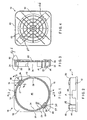
- FIG. 1 is a top plan view of the base 10 of the semiconductor wafer containment device or wafer box of the present invention.
- Base 10 includes a generally planar square floor 12 formed from sides 14, 16, 18, 20.
- Inner and outer concentric cylindrical walls 22, 24 rise from the planar floor 12.
- Male aligning elements 15, 19 are formed at central locations on sides 14, 18 outwardly from outer concentric cylindrical wall 24.
- Inner and outer concentric cylindrical walls 22, 24 include slots 26, 28 at opposed corners and aligned gaps forming openings 34, 36 which are opposed by 180° from each other.
- the portion of inner concentric cylindrical wall 22 immediately adjacent to openings 34, 36 includes partial notch 38.
- a wafer containment space 40 is formed within inner concentric cylindrical wall 22.
- Wafer containment space 40 may be adapted to an eight inch diameter wafer, although a range of other sizes is certainly possible.
- Pivoting latch elements 44, 46 terminating in inverted ledges 48, 50 are journaled from diagonally opposite corners of floor 12 and pivot radially through slots 26, 28.
- Pivoting latch elements 44, 46 have extruded padded spacer elements 52, 53 on the interior surface thereof for the engagement of the semiconductor wafers 100 (see Figures 14 , 16 and 18-21 ).
- pivoting latch elements 44, 46 include T-shaped grooves 54, 55 for receiving complementary T-shaped flanges 56, 58 on the exterior of extruded padded elements 52, 53 (see Fig. 22 ).
- Extruded padded spacer elements 52, 53 need to be soft to cushion the semiconductor wafers 100 but firm enough to prevent movement as extruded padded spacer elements 52, 53 act like a spring gently pushing on the stack of semiconductor wafers 100.
- a typical material for the extruded padded spacer elements 52, 53 would be Kraton but one skilled in the art would recognize a range of equivalent materials after study of this disclosure.
- Figure 4 shows the bottom plan view of base 10, including peripheral foot structure 60 which extends around the periphery of floor 12 in order to provide an offset between floor 12 and the surface (not shown) upon which base 10 is resting. Additionally, lattice work 62 is formed on the bottom of floor 12. Furthermore, Figure 4 shows the underside of the pivot axes 64, 66 of pivoting latch elements 44, 46.
- Figures 23 and 24 show an alternative embodiment of base 10, with four slots 26, 27, 28, 29 with four pivot axes 64, 65, 66, 67 for receiving pivoting latch elements. Such a configuration is typically used for larger wafer sizes.
- FIG. 5 shows cross-sectional detail of the pivot axis 64 (which likewise applies to pivot axis 66) of pivoting latch element 44.
- Pivoting latch element 44 includes major arm 57 which is attached to minor arm 59. Minor arm 59 is seated within pocket 61 of base 10 and terminates at pivot axis 64.
- Major arm 57 is attached to minor arm 59 at an obtuse angle slightly greater than 90°. This obtuse angle, along with other dimensions, determines or limits the outward angle at which major arm 57 of pivoting latch element 44 can extend when minor arm 59 rests on the floor of pocket 61 thereby resulting in pivoting latch element 44 being in its outward position such as shown in Figures 14 , 16 , 18 and 21 .
- the limiting of the outward angle or outward position is necessary to ensure that the structures of the lid 70, as described hereinafter, can capture the pivoting latch elements 44, 46 in the outward position and urge them into the upright detent position.
- Figure 6 shows some detail of inner and outer concentric cylindrical walls 22, 24.
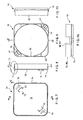
- FIGS 7-10 show the lid 70 of the semiconductor wafer containment device or wafer box of the present invention.
- Lid 70 includes top planar square surface 72 surrounded by peripheral upwardly extending ledge 74 and bounded by generally square outer skirt wall 82.
- Cylindrical wall 80 is formed inwardly of outer skirt wall 82.
- Slots 76, 78 are formed on opposite corners of top planar square surface 72. Slots are formed at each corner for a lid 70 adaptable to the embodiment of the base 10 shown in Figures 23 and 24 .
- Ramps 77, 79 are formed between slots 76, 78 and outer skirt wall 82.
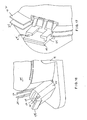
- ramps 77, 79 capture the pivoting latch elements 44, 46 (see Figure 18 ) from a radially outward pivoted position (see Figure 21 ) and urge (see Figure 19 ) pivoting latch elements 44, 46 into an upright configuration so as to be received by slots 76, 78 to form a detent configuration (see Figure 20 ), thereby urging extruded padded spacer elements 52, 53 to impinge against semiconductor wafers 100 in wafer containment space 40.
- Finger gripping elements 81, 83 are formed radially inward from slots 76, 78 to allow a user to manually urge pivoting latch elements 44, 46 inwardly to release from slots 76, 78 when the lid 70 is to be removed.
- Outer cylindrical wall 80 is formed on the lower side of top planar square surface 72.
- Outer cylindrical wall 80 further includes female aligning elements 85, 87 which are oriented 180° apart. In the installed position, outer cylindrical wall 80 is immediately outwardly concentrically adjacent from outer concentric cylindrical wall 24 and female aligning elements 85, 87 are engaged with male aligning elements 15, 19.
- the user would typically start with an empty base 10 (that is, with no semiconductor wafers 100 in wafer containment space 40), with pivoting latch elements 44, 46 in their outward positions.
- the user would then manually or with automated equipment, place semiconductor wafers 100 into wafer containment space 40 and place lid 70 over base 10 so as to capture pivoting latch elements 44, 46 and urge them to an upright detent position with extruded padded spacer elements 52, 53 impinging against semiconductor wafers 100 as shown in the sequence from Figures 18-20 and as described above.
- the wafer containment box is then typically transported.
- Lid 70 may be removed manually by squeezing the pivoting latch elements 44, 46 toward the finger gripping elements 81, 83 to release the pivoting latch elements 44, 46 from lid 70 thereby allowing the pivoting latch elements 44, 46 to pivot to an outward position (such as shown in Figure 21 ) thereby allowing easy access to the semiconductor wafers 100.
Landscapes
- Packaging Frangible Articles (AREA)
- Container, Conveyance, Adherence, Positioning, Of Wafer (AREA)
Abstract
Description
- The present invention relates to a containment device or wafer box for semiconductor wafers. More particularly, this containment device has latch elements which pivot radially through slots in a cylindrical wall. The latch elements include spacer elements on the inside surface to engage semiconductor wafers within the cylindrical wall when the latch elements are in their upright position, detent engaged with the lid element. When the latch elements are not detent engaged with the lid, the latch elements along with the spacer elements are free to pivot radially outwardly to provide free access to the semiconductor wafers.
- The prior art contains a variety of designs for the containment and transport of semiconductor wafers. These designs must provide both electrostatic and mechanical protection for the wafers contained therein. Preferably, such containment devices should be easily adaptable to various automated apparatus which load or unload the semiconductor wafers. Such containment devices should have a simple design which is reliable and economical to mass produce.
- Examples of some prior art are
U.S. Patent No. 6,193,068 entitled "Containment Device for Retaining Semiconductor Wafers" issued on February 27, 2001 to Lewis et al.;U.S. Patent No. 6,286,684 entitled "Protective System for Integrated Circuit (IC) Wafers Retained Within Containers Designed for Storage and Shipment" issued on September 11, 2001 to Brooks et al;U.S. Patent No. 6,003,674 entitled "Method and Apparatus for Packing Contaminant-Sensitive Articles and Resulting Package" issued on December 21, 1999 to Brooks; andU.S. Patent No. 5,724,748 entitled "Apparatus for Packaging Contaminant-Sensitive Articles and Resulting Package" issued on March 10, 1998 to Brook et al. -
US6550619 discloses a containment device for semiconductor wafers, comprising: - a base including at least one cylindrical wall extending therefrom, said at least one cylindrical wall forming a wafer containment space therewithin.
- Such a device is, according to the present invention, characterised by
said at least one cylindrical wall including slots through which latch elements pivot radially; and
a lid which includes means for capturing said latch elements in an outwardly pivoted position and for urging said latch elements to a radially inward position so as to engage semiconductor wafers within said wafer containment space, said latch elements thereby detent engaging said lid, said lid forming a top of the containment device when said base and said lid are detent engaged together. - The latch elements include spacer elements on the inward surface thereof. When the latch elements are detent engaged by the lid, the latch elements are in an upright position with the spacer elements extending into the wafer containment space formed within the cylindrical wall. The spacer elements are thereby urged against the semiconductor wafers in the wafer containment space. When the latch elements are free of engagement with the lid, the latch elements are free to pivot radially outwardly to release engagement with the semiconductor wafers to allow the semiconductor wafers to be removed by a manual or automated process for further processing. Typically, the spacer elements on the interior of the latch elements are formed of somewhat soft or spongy material so as to engage the semiconductor wafers without damaging the wafers.
- Further objects and advantages will become apparent from the following description and from the accompanying drawings, wherein:
-
Figure 1 is a top plan view of the base of the semiconductor wafer containment device of the present invention. -
Figure 2 is a side plan view of the base of the semiconductor wafer containment device of the present invention. -
Figure 3 is a cross-sectional view along plane 3-3 ofFigure 1 . -
Figure 4 is a bottom plan view of the base of the base of the semiconductor wafer containment device of the present invention. -
Figure 5 is a cross-sectional view alone plane 5-5 ofFigure 1 . -
Figure 6 is a cross-sectional view further detailing a portion ofFigure 3 . -
Figure 7 is a top plan view of the lid of the semiconductor wafer containment device of the present invention. -
Figure 8 is a cross-sectional view along plane 8-8 ofFigure 7 . -
Figure 9 is a bottom plan view of the lid ofFigure 7 . -
Figure 10 is a front plan view of the lid ofFigure 7 . -
Figure 11 is a side plan view of the lid ofFigure 7 . -
Figure 12 is a cross-sectional view along plane 12-12 ofFigure 7 . -
Figure 13 is a cross-sectional view further detailing a portion ofFigure 8 . -
Figure 14 is a perspective view of the pivoting latch element of the present invention, in an upright position so that the spacer element engages the semiconductor wafers. -
Figure 15 is a perspective view of a portion of the underside of the base of the present invention, showing the pivoting mechanism of the pivoting latch element. -
Figure 16 is a perspective view of the pivoting latch element of the present invention, in an outwardly pivoted position so that the spacer element is substantially free of engagement with the semiconductor wafers. -
Figure 17 is a perspective view of the pivoting latch element of the present invention, with the spacer element removed thereby showing the pivoting mechanism. -
Figure 18 is a perspective, partially cut-away, view of the lid of the semiconductor wafer containment device being brought into engagement with the base, whereby a ramp in the interior of the lid urges the pivoting latch element from an outwardly pivoted position toward the upright position as the lid is brought into engagement with the base. -
Figure 19 is a perspective, partially cut-away, view of the lid of the semiconductor wafer containment device being brought further into engagement with the base, whereby the pivoting latch element is almost in its upright position, and approaching engagement with the slot in the lid. -
Figure 20 is a perspective, partially cut-away, view of the lid of the semiconductor wafer containment device engaging the pivoting latch element so that the pivoting latch element is in its upright position and the spacer element is urged against the semiconductor wafers. -
Figure 21 is a perspective, partially cut-away, view of the lid of the semiconductor wafer containment device free of engagement with pivoting latch element the base so that the pivoting latch element pivots outwardly thereby moving the spacer element away from the semiconductor wafers. -
Figure 22 is a perspective view of the spacer element -
Figure 23 is a top perspective view of the base of an alternative embodiment of the semiconductor wafer containment device of the present invention, configured for use with four pivoting latch elements. -
Figure 24 is a bottom perspective view of the base of an alternative embodiment of the semiconductor wafer containment device of the present invention, configured for use with four pivoting latch elements. - Referring now to the drawings in detail wherein like numerals refer to like elements throughout the several views, one sees that
Figure 1 is a top plan view of thebase 10 of the semiconductor wafer containment device or wafer box of the present invention.Base 10 includes a generally planarsquare floor 12 formed fromsides cylindrical walls planar floor 12. Male aligningelements sides cylindrical wall 24. Inner and outer concentriccylindrical walls slots gaps forming openings Figure 3 , the portion of inner concentriccylindrical wall 22 immediately adjacent toopenings partial notch 38. Awafer containment space 40 is formed within inner concentriccylindrical wall 22.Wafer containment space 40 may be adapted to an eight inch diameter wafer, although a range of other sizes is certainly possible. Pivotinglatch elements ledges floor 12 and pivot radially throughslots latch elements spacer elements Figures 14 ,16 and18-21 ). As shown inFigures 16 and 17 , pivotinglatch elements shaped grooves shaped flanges padded elements 52, 53 (seeFig. 22 ). - Extruded
padded spacer elements semiconductor wafers 100 but firm enough to prevent movement as extruded paddedspacer elements semiconductor wafers 100. A typical material for the extruded paddedspacer elements -
Figure 4 shows the bottom plan view ofbase 10, includingperipheral foot structure 60 which extends around the periphery offloor 12 in order to provide an offset betweenfloor 12 and the surface (not shown) upon whichbase 10 is resting. Additionally,lattice work 62 is formed on the bottom offloor 12. Furthermore,Figure 4 shows the underside of thepivot axes latch elements -
Figures 23 and 24 show an alternative embodiment ofbase 10, with fourslots pivot axes -
Figure 5 shows cross-sectional detail of the pivot axis 64 (which likewise applies to pivot axis 66) of pivotinglatch element 44. Pivotinglatch element 44 includes major arm 57 which is attached tominor arm 59.Minor arm 59 is seated within pocket 61 ofbase 10 and terminates atpivot axis 64. Major arm 57 is attached tominor arm 59 at an obtuse angle slightly greater than 90°. This obtuse angle, along with other dimensions, determines or limits the outward angle at which major arm 57 of pivotinglatch element 44 can extend whenminor arm 59 rests on the floor of pocket 61 thereby resulting in pivotinglatch element 44 being in its outward position such as shown inFigures 14 ,16 ,18 and21 . The limiting of the outward angle or outward position is necessary to ensure that the structures of thelid 70, as described hereinafter, can capture the pivotinglatch elements -
Figure 6 shows some detail of inner and outer concentriccylindrical walls -
Figures 7-10 show thelid 70 of the semiconductor wafer containment device or wafer box of the present invention.Lid 70 includes top planarsquare surface 72 surrounded by peripheral upwardly extendingledge 74 and bounded by generally squareouter skirt wall 82.Cylindrical wall 80 is formed inwardly ofouter skirt wall 82.Slots square surface 72. Slots are formed at each corner for alid 70 adaptable to the embodiment of the base 10 shown inFigures 23 and 24 .Ramps slots outer skirt wall 82. In reaching the installed position ofFigure 20 , ramps 77, 79 capture the pivotinglatch elements 44, 46 (seeFigure 18 ) from a radially outward pivoted position (seeFigure 21 ) and urge (seeFigure 19 ) pivotinglatch elements slots Figure 20 ), thereby urging extruded paddedspacer elements semiconductor wafers 100 inwafer containment space 40. - Finger
gripping elements slots latch elements slots lid 70 is to be removed. Outercylindrical wall 80 is formed on the lower side of top planarsquare surface 72. Outercylindrical wall 80 further includes female aligningelements 85, 87 which are oriented 180° apart. In the installed position, outercylindrical wall 80 is immediately outwardly concentrically adjacent from outer concentriccylindrical wall 24 and female aligningelements 85, 87 are engaged withmale aligning elements - To use the wafer containment box of the present invention, the user would typically start with an empty base 10 (that is, with no
semiconductor wafers 100 in wafer containment space 40), with pivotinglatch elements place semiconductor wafers 100 intowafer containment space 40 andplace lid 70 overbase 10 so as to capture pivotinglatch elements spacer elements semiconductor wafers 100 as shown in the sequence fromFigures 18-20 and as described above. The wafer containment box is then typically transported.Lid 70 may be removed manually by squeezing the pivotinglatch elements finger gripping elements latch elements lid 70 thereby allowing the pivotinglatch elements Figure 21 ) thereby allowing easy access to thesemiconductor wafers 100. - Thus the several aforementioned objects and advantages are most effectively attained. Although a single preferred embodiment of the invention has been disclosed and described in detail herein, it should be understood that this invention is in no sense limited thereby and its scope is to be determined by that of the appended claims.
Claims (10)
- A containment device for semiconductor wafers, comprising:a base (10) including at least one cylindrical wall (22, 24) extending therefrom, said at least one cylindrical wall forming a wafer containment space (40) therewithin, characterised bysaid at least one cylindrical wall (22, 24) including slots (26, 28) through which latch elements (44, 46) pivot radially; anda lid (70) which includes means (77, 79) for capturing said latch elements (44, 46) in an outwardly pivoted position and for urging said latch elements to a radially inward position so as to engage semiconductor wafers (100) within said wafer containment space (40), said latch elements thereby detent engaging said lid, said lid forming a top of the containment device when said base (10) and said lid are detent engaged together.
- The containment device for semiconductor wafers of Claim 1 wherein said at least one cylindrical wall (22,24) extends perpendicularly from said base (10).
- The containment device for semiconductor wafers of Claim 2 wherein said latch elements (44, 46) pivot between an outward position which is substantially away from said wafer containment space (40) and an inward upright position which impinges said wafer containment space (40).
- The containment device for semiconductor wafers of Claim 3 wherein said means for capturing and urging includes ramps (77, 79) formed from an exterior portion of said lid to slots (76, 78) formed inwardly adjacent from said exterior portion, wherein said ramps capture said latch elements in said outward position and said slots detent engage said latch elements in said upright position.
- The containment device for semiconductor wafers of Claim 4 wherein said latch elements (44, 46) include an exterior relatively rigid portion and an interior spacer element (52, 53), said interior spacer element for impinging into said wafer containment space.
- The containment device for semiconductor wafers of Claim 5 wherein said relatively rigid portion includes a groove (54, 55) and said interior spacer element includes a flange (56, 58) for engaging said groove.
- The containment device for semiconductor wafers of Claim 6 wherein said pivoting latch elements (44, 46) include a first arm (57) and a second arm (59) at an obtuse angle to each other, wherein said first arm (57) includes an element (50) for detent engaging said lid (70) and said second arm (59) includes a pivot axis (64).
- The containment device for semiconductor wafers of Claim 7 wherein said second arm (59) travels within a pocket (61) in said base (10).
- The containment device for semiconductor wafers of Claim 1 wherein said lid (70) includes a lid cylindrical wall (82) which, when said base (10) and said lid (70) are detent engaged together, fits immediately outwardly adjacent from said at least one cylindrical wall of said base.
- The containment device for semiconductor wafers of Claim 9 wherein male aligning elements (15, 19) are formed outward of said at least one cylindrical wall (22, 24) and female aligning elements (85, 87) are formed on said lid cylindrical wall, whereby said male aligning elements and said female aligning elements engage when said base (10) and said lid (70) are detent engaged together.
Applications Claiming Priority (3)
| Application Number | Priority Date | Filing Date | Title |
|---|---|---|---|
| US47908603P | 2003-06-17 | 2003-06-17 | |
| US10/787,489 US6988621B2 (en) | 2003-06-17 | 2004-02-25 | Reduced movement wafer box |
| PCT/US2004/014659 WO2005001890A2 (en) | 2003-06-17 | 2004-05-11 | Wafer box with radially pivoting latch elements |
Publications (3)
| Publication Number | Publication Date |
|---|---|
| EP1638864A2 EP1638864A2 (en) | 2006-03-29 |
| EP1638864A4 EP1638864A4 (en) | 2008-07-30 |
| EP1638864B1 true EP1638864B1 (en) | 2011-11-30 |
Family
ID=33519329
Family Applications (1)
| Application Number | Title | Priority Date | Filing Date |
|---|---|---|---|
| EP04751855A Expired - Lifetime EP1638864B1 (en) | 2003-06-17 | 2004-05-11 | Wafer box with radially pivoting latch elements |
Country Status (6)
| Country | Link |
|---|---|
| US (2) | US6988621B2 (en) |
| EP (1) | EP1638864B1 (en) |
| JP (1) | JP4564004B2 (en) |
| KR (1) | KR20060026423A (en) |
| AT (1) | ATE535936T1 (en) |
| WO (1) | WO2005001890A2 (en) |
Families Citing this family (17)
| Publication number | Priority date | Publication date | Assignee | Title |
|---|---|---|---|---|
| US7578392B2 (en) * | 2003-06-06 | 2009-08-25 | Convey Incorporated | Integrated circuit wafer packaging system and method |
| US6988621B2 (en) * | 2003-06-17 | 2006-01-24 | Illinois Tool Works Inc. | Reduced movement wafer box |
| US7431162B2 (en) * | 2005-07-15 | 2008-10-07 | Illinois Tool Works Inc. | Shock absorbing horizontal transport wafer box |
| FR2896912B1 (en) * | 2005-12-09 | 2008-11-28 | Alcatel Sa | SEALED ENCLOSURE FOR TRANSPORTING AND STORING SEMICONDUCTOR SUBSTRATES |
| WO2009048456A1 (en) * | 2007-10-12 | 2009-04-16 | Peak Plastic & Metal Products (International) Limited | Wafer container with staggered wall structure |
| US8109390B2 (en) * | 2009-08-26 | 2012-02-07 | Texchem Advanced Products Incorporated Sdn Bhd | Wafer container with overlapping wall structure |
| US8556079B2 (en) * | 2009-08-26 | 2013-10-15 | Texchem Advanced Products Incorporated Sdn Bhd | Wafer container with adjustable inside diameter |
| US8813964B2 (en) * | 2009-08-26 | 2014-08-26 | Texchem Advanced Products Incorporated Sdn. Bhd. | Wafer container with recessed latch |
| WO2012135863A2 (en) * | 2011-04-01 | 2012-10-04 | Entegris, Inc. | Substrate shipper with locking device |
| CN103074610A (en) * | 2012-08-28 | 2013-05-01 | 光达光电设备科技(嘉兴)有限公司 | Substrate supporting structure and reaction chamber containing the same |
| WO2014062956A1 (en) * | 2012-10-19 | 2014-04-24 | Entegris, Inc. | Reticle pod with cover to baseplate alignment system |
| JP6258069B2 (en) * | 2014-02-26 | 2018-01-10 | 信越ポリマー株式会社 | Substrate storage container |
| US10153187B2 (en) * | 2014-11-11 | 2018-12-11 | Applied Materials, Inc. | Methods and apparatus for transferring a substrate |
| JP6767297B2 (en) * | 2017-03-31 | 2020-10-14 | アキレス株式会社 | Wafer storage container |
| KR102595523B1 (en) * | 2021-09-07 | 2023-10-30 | 주식회사 삼에스코리아 | Waper shipping box |
| KR102595526B1 (en) * | 2021-09-07 | 2023-10-30 | 주식회사 삼에스코리아 | Waper shipping box |
| EP4503107A1 (en) * | 2022-03-30 | 2025-02-05 | Achilles Corporation | Semiconductor wafer transfer container |
Family Cites Families (22)
| Publication number | Priority date | Publication date | Assignee | Title |
|---|---|---|---|---|
| US3691294A (en) * | 1970-10-05 | 1972-09-12 | Coil Sales Inc | Package for encapsulated electrical components |
| US3997072A (en) * | 1975-02-24 | 1976-12-14 | General Electric Company | Compactor container with removable bottom |
| JP2941125B2 (en) * | 1992-08-15 | 1999-08-25 | アキレス株式会社 | Semiconductor wafer storage container |
| US5366079A (en) * | 1993-08-19 | 1994-11-22 | Taiwan Semiconductor Manufacturing Company | Integrated circuit wafer and retainer element combination |
| JPH08236605A (en) * | 1995-02-28 | 1996-09-13 | Komatsu Electron Metals Co Ltd | Semiconductor wafer storage case |
| US5553711A (en) * | 1995-07-03 | 1996-09-10 | Taiwan Semiconductor Manufacturing Company | Storage container for integrated circuit semiconductor wafers |
| JPH0986588A (en) * | 1995-09-21 | 1997-03-31 | Komatsu Kasei Kk | Lamination type packaging container |
| US5611448A (en) * | 1995-09-25 | 1997-03-18 | United Microelectronics Corporation | Wafer container |
| US6003674A (en) | 1996-05-13 | 1999-12-21 | Brooks; Ray Gene | Method and apparatus for packing contaminant-sensitive articles and resulting package |
| US5724748A (en) * | 1996-07-24 | 1998-03-10 | Brooks; Ray G. | Apparatus for packaging contaminant-sensitive articles and resulting package |
| US6193068B1 (en) * | 1998-05-07 | 2001-02-27 | Texas Instruments Incorporated | Containment device for retaining semiconductor wafers |
| US6341695B1 (en) * | 1998-05-07 | 2002-01-29 | Texas Instruments Incorporated | Containment device for retaining semiconductor wafers |
| US6193090B1 (en) * | 1999-04-06 | 2001-02-27 | 3M Innovative Properties Company | Reusable container |
| DE60044028D1 (en) * | 1999-07-23 | 2010-04-29 | Ray G Brooks | SECURING SYSTEM FOR WAFER WITH INTEGRATED CIRCUIT (IC) |
| US6550619B2 (en) * | 2000-05-09 | 2003-04-22 | Entergris, Inc. | Shock resistant variable load tolerant wafer shipper |
| JP4480296B2 (en) * | 2001-05-09 | 2010-06-16 | アキレス株式会社 | Electronic material storage container |
| US6988620B2 (en) * | 2002-09-06 | 2006-01-24 | E.Pak International, Inc. | Container with an adjustable inside dimension that restricts movement of items within the container |
| JP2004266181A (en) * | 2003-03-04 | 2004-09-24 | Nec Electronics Corp | Semiconductor substrate storage container |
| US6988621B2 (en) * | 2003-06-17 | 2006-01-24 | Illinois Tool Works Inc. | Reduced movement wafer box |
| CN100363243C (en) * | 2003-06-17 | 2008-01-23 | 伊利诺斯器械工程公司 | Wafer cassette with reduced movement |
| US6915906B2 (en) * | 2003-07-14 | 2005-07-12 | Peak Plastic & Metal Products (International) Limited | Wafer storage container with wafer positioning posts |
| US7225929B2 (en) * | 2004-12-30 | 2007-06-05 | Illinois Tool Works Inc. | Adjustable height wafer box |
-
2004
- 2004-02-25 US US10/787,489 patent/US6988621B2/en not_active Expired - Fee Related
- 2004-05-11 AT AT04751855T patent/ATE535936T1/en active
- 2004-05-11 EP EP04751855A patent/EP1638864B1/en not_active Expired - Lifetime
- 2004-05-11 JP JP2006517114A patent/JP4564004B2/en not_active Expired - Fee Related
- 2004-05-11 WO PCT/US2004/014659 patent/WO2005001890A2/en not_active Ceased
- 2004-05-11 US US10/507,471 patent/US7565980B2/en not_active Expired - Lifetime
- 2004-05-11 KR KR1020057024172A patent/KR20060026423A/en not_active Withdrawn
Also Published As
| Publication number | Publication date |
|---|---|
| WO2005001890A2 (en) | 2005-01-06 |
| JP2006527921A (en) | 2006-12-07 |
| KR20060026423A (en) | 2006-03-23 |
| US7565980B2 (en) | 2009-07-28 |
| US6988621B2 (en) | 2006-01-24 |
| JP4564004B2 (en) | 2010-10-20 |
| EP1638864A2 (en) | 2006-03-29 |
| US20040256285A1 (en) | 2004-12-23 |
| US20060180499A1 (en) | 2006-08-17 |
| ATE535936T1 (en) | 2011-12-15 |
| EP1638864A4 (en) | 2008-07-30 |
| WO2005001890A3 (en) | 2005-03-24 |
Similar Documents
| Publication | Publication Date | Title |
|---|---|---|
| US7565980B2 (en) | Wafer box with radially pivoting latch elements | |
| US6216873B1 (en) | SMIF container including a reticle support structure | |
| JP3202991B2 (en) | Closed, sealable and scavengable semiconductor wafer holding device | |
| EP3231009B1 (en) | Horizontal substrate container with integral corner spring for substrate containment | |
| US6644477B2 (en) | Wafer container cushion system | |
| US7040487B2 (en) | Protective shipper | |
| JP4741180B2 (en) | Apparatus and method for protecting and transporting a reticle | |
| US4859137A (en) | Apparatus for transporting a holder between a port opening of a standardized mechanical interface system and a loading and unloading station | |
| TW502369B (en) | System for preventing improper insertion of FOUP door into FOUP | |
| WO1997008746A1 (en) | Container for housing semiconductor wafers, structure for housing semiconductor wafers, and method of putting in and taking out semiconductor wafers | |
| US20030012628A1 (en) | 300MM single stackable film frame carrier | |
| US7066708B1 (en) | Methods and apparatus for retaining a tray stack having a plurality of trays for carrying microelectric devices | |
| CN104787502A (en) | Wafer container with adjustable inside diameter | |
| US20140076774A1 (en) | Automated Wafer Container with Equipment Interface | |
| KR20040019264A (en) | Wafer carrier with stacking adaptor plate | |
| US6237771B1 (en) | Wafer shipping container | |
| CN100361879C (en) | Wafer Cassettes with Radial Rotation Latching Elements | |
| WO1992021145A1 (en) | Single wafer robotic package | |
| CN1845860B (en) | Low cost wafer box improvements | |
| EP4575635A1 (en) | Stocker system with a stack of reticle storage pods with prevention of storage pod horizontal movement | |
| US6886696B2 (en) | Wafer container with removable sidewalls | |
| US12106988B2 (en) | Separators for handling, transporting, or storing semiconductor wafers | |
| KR100335815B1 (en) | Sealable, washable semiconductor wafer holder | |
| CN121171943A (en) | Wafer container enclosure and wafer container transfer method |
Legal Events
| Date | Code | Title | Description |
|---|---|---|---|
| PUAI | Public reference made under article 153(3) epc to a published international application that has entered the european phase |
Free format text: ORIGINAL CODE: 0009012 |
|
| 17P | Request for examination filed |
Effective date: 20051227 |
|
| AK | Designated contracting states |
Kind code of ref document: A2 Designated state(s): AT BE BG CH CY CZ DE DK EE ES FI FR GB GR HU IE IT LI LU MC NL PL PT RO SE SI SK TR |
|
| DAX | Request for extension of the european patent (deleted) | ||
| A4 | Supplementary search report drawn up and despatched |
Effective date: 20080626 |
|
| RIC1 | Information provided on ipc code assigned before grant |
Ipc: B65D 85/90 20060101ALI20080620BHEP Ipc: H01L 21/68 20060101AFI20080620BHEP |
|
| 17Q | First examination report despatched |
Effective date: 20101008 |
|
| GRAP | Despatch of communication of intention to grant a patent |
Free format text: ORIGINAL CODE: EPIDOSNIGR1 |
|
| GRAS | Grant fee paid |
Free format text: ORIGINAL CODE: EPIDOSNIGR3 |
|
| GRAA | (expected) grant |
Free format text: ORIGINAL CODE: 0009210 |
|
| AK | Designated contracting states |
Kind code of ref document: B1 Designated state(s): AT BE BG CH CY CZ DE DK EE ES FI FR GB GR HU IE IT LI LU MC NL PL PT RO SE SI SK TR |
|
| REG | Reference to a national code |
Ref country code: CH Ref legal event code: EP Ref country code: GB Ref legal event code: FG4D |
|
| REG | Reference to a national code |
Ref country code: IE Ref legal event code: FG4D |
|
| REG | Reference to a national code |
Ref country code: DE Ref legal event code: R096 Ref document number: 602004035527 Country of ref document: DE Effective date: 20120202 |
|
| REG | Reference to a national code |
Ref country code: NL Ref legal event code: VDEP Effective date: 20111130 |
|
| PG25 | Lapsed in a contracting state [announced via postgrant information from national office to epo] |
Ref country code: NL Free format text: LAPSE BECAUSE OF FAILURE TO SUBMIT A TRANSLATION OF THE DESCRIPTION OR TO PAY THE FEE WITHIN THE PRESCRIBED TIME-LIMIT Effective date: 20111130 Ref country code: BE Free format text: LAPSE BECAUSE OF FAILURE TO SUBMIT A TRANSLATION OF THE DESCRIPTION OR TO PAY THE FEE WITHIN THE PRESCRIBED TIME-LIMIT Effective date: 20111130 Ref country code: GR Free format text: LAPSE BECAUSE OF FAILURE TO SUBMIT A TRANSLATION OF THE DESCRIPTION OR TO PAY THE FEE WITHIN THE PRESCRIBED TIME-LIMIT Effective date: 20120301 Ref country code: SI Free format text: LAPSE BECAUSE OF FAILURE TO SUBMIT A TRANSLATION OF THE DESCRIPTION OR TO PAY THE FEE WITHIN THE PRESCRIBED TIME-LIMIT Effective date: 20111130 Ref country code: PT Free format text: LAPSE BECAUSE OF FAILURE TO SUBMIT A TRANSLATION OF THE DESCRIPTION OR TO PAY THE FEE WITHIN THE PRESCRIBED TIME-LIMIT Effective date: 20120330 Ref country code: SE Free format text: LAPSE BECAUSE OF FAILURE TO SUBMIT A TRANSLATION OF THE DESCRIPTION OR TO PAY THE FEE WITHIN THE PRESCRIBED TIME-LIMIT Effective date: 20111130 |
|
| PG25 | Lapsed in a contracting state [announced via postgrant information from national office to epo] |
Ref country code: CY Free format text: LAPSE BECAUSE OF FAILURE TO SUBMIT A TRANSLATION OF THE DESCRIPTION OR TO PAY THE FEE WITHIN THE PRESCRIBED TIME-LIMIT Effective date: 20111130 |
|
| PG25 | Lapsed in a contracting state [announced via postgrant information from national office to epo] |
Ref country code: EE Free format text: LAPSE BECAUSE OF FAILURE TO SUBMIT A TRANSLATION OF THE DESCRIPTION OR TO PAY THE FEE WITHIN THE PRESCRIBED TIME-LIMIT Effective date: 20111130 Ref country code: BG Free format text: LAPSE BECAUSE OF FAILURE TO SUBMIT A TRANSLATION OF THE DESCRIPTION OR TO PAY THE FEE WITHIN THE PRESCRIBED TIME-LIMIT Effective date: 20120229 Ref country code: SK Free format text: LAPSE BECAUSE OF FAILURE TO SUBMIT A TRANSLATION OF THE DESCRIPTION OR TO PAY THE FEE WITHIN THE PRESCRIBED TIME-LIMIT Effective date: 20111130 Ref country code: DK Free format text: LAPSE BECAUSE OF FAILURE TO SUBMIT A TRANSLATION OF THE DESCRIPTION OR TO PAY THE FEE WITHIN THE PRESCRIBED TIME-LIMIT Effective date: 20111130 Ref country code: CZ Free format text: LAPSE BECAUSE OF FAILURE TO SUBMIT A TRANSLATION OF THE DESCRIPTION OR TO PAY THE FEE WITHIN THE PRESCRIBED TIME-LIMIT Effective date: 20111130 |
|
| PG25 | Lapsed in a contracting state [announced via postgrant information from national office to epo] |
Ref country code: PL Free format text: LAPSE BECAUSE OF FAILURE TO SUBMIT A TRANSLATION OF THE DESCRIPTION OR TO PAY THE FEE WITHIN THE PRESCRIBED TIME-LIMIT Effective date: 20111130 Ref country code: IT Free format text: LAPSE BECAUSE OF FAILURE TO SUBMIT A TRANSLATION OF THE DESCRIPTION OR TO PAY THE FEE WITHIN THE PRESCRIBED TIME-LIMIT Effective date: 20111130 Ref country code: RO Free format text: LAPSE BECAUSE OF FAILURE TO SUBMIT A TRANSLATION OF THE DESCRIPTION OR TO PAY THE FEE WITHIN THE PRESCRIBED TIME-LIMIT Effective date: 20111130 |
|
| REG | Reference to a national code |
Ref country code: AT Ref legal event code: MK05 Ref document number: 535936 Country of ref document: AT Kind code of ref document: T Effective date: 20111130 |
|
| PLBE | No opposition filed within time limit |
Free format text: ORIGINAL CODE: 0009261 |
|
| STAA | Information on the status of an ep patent application or granted ep patent |
Free format text: STATUS: NO OPPOSITION FILED WITHIN TIME LIMIT |
|
| 26N | No opposition filed |
Effective date: 20120831 |
|
| REG | Reference to a national code |
Ref country code: DE Ref legal event code: R097 Ref document number: 602004035527 Country of ref document: DE Effective date: 20120831 |
|
| PG25 | Lapsed in a contracting state [announced via postgrant information from national office to epo] |
Ref country code: MC Free format text: LAPSE BECAUSE OF NON-PAYMENT OF DUE FEES Effective date: 20120531 |
|
| REG | Reference to a national code |
Ref country code: CH Ref legal event code: PL |
|
| GBPC | Gb: european patent ceased through non-payment of renewal fee |
Effective date: 20120511 |
|
| PG25 | Lapsed in a contracting state [announced via postgrant information from national office to epo] |
Ref country code: AT Free format text: LAPSE BECAUSE OF FAILURE TO SUBMIT A TRANSLATION OF THE DESCRIPTION OR TO PAY THE FEE WITHIN THE PRESCRIBED TIME-LIMIT Effective date: 20111130 Ref country code: CH Free format text: LAPSE BECAUSE OF NON-PAYMENT OF DUE FEES Effective date: 20120531 Ref country code: LI Free format text: LAPSE BECAUSE OF NON-PAYMENT OF DUE FEES Effective date: 20120531 |
|
| REG | Reference to a national code |
Ref country code: IE Ref legal event code: MM4A |
|
| REG | Reference to a national code |
Ref country code: FR Ref legal event code: ST Effective date: 20130131 |
|
| REG | Reference to a national code |
Ref country code: DE Ref legal event code: R119 Ref document number: 602004035527 Country of ref document: DE Effective date: 20121201 |
|
| PG25 | Lapsed in a contracting state [announced via postgrant information from national office to epo] |
Ref country code: GB Free format text: LAPSE BECAUSE OF NON-PAYMENT OF DUE FEES Effective date: 20120511 Ref country code: IE Free format text: LAPSE BECAUSE OF NON-PAYMENT OF DUE FEES Effective date: 20120511 Ref country code: FR Free format text: LAPSE BECAUSE OF NON-PAYMENT OF DUE FEES Effective date: 20120531 Ref country code: ES Free format text: LAPSE BECAUSE OF FAILURE TO SUBMIT A TRANSLATION OF THE DESCRIPTION OR TO PAY THE FEE WITHIN THE PRESCRIBED TIME-LIMIT Effective date: 20120311 |
|
| PG25 | Lapsed in a contracting state [announced via postgrant information from national office to epo] |
Ref country code: FI Free format text: LAPSE BECAUSE OF FAILURE TO SUBMIT A TRANSLATION OF THE DESCRIPTION OR TO PAY THE FEE WITHIN THE PRESCRIBED TIME-LIMIT Effective date: 20111130 Ref country code: DE Free format text: LAPSE BECAUSE OF NON-PAYMENT OF DUE FEES Effective date: 20121201 |
|
| PG25 | Lapsed in a contracting state [announced via postgrant information from national office to epo] |
Ref country code: TR Free format text: LAPSE BECAUSE OF FAILURE TO SUBMIT A TRANSLATION OF THE DESCRIPTION OR TO PAY THE FEE WITHIN THE PRESCRIBED TIME-LIMIT Effective date: 20111130 |
|
| PG25 | Lapsed in a contracting state [announced via postgrant information from national office to epo] |
Ref country code: LU Free format text: LAPSE BECAUSE OF NON-PAYMENT OF DUE FEES Effective date: 20120511 |
|
| PG25 | Lapsed in a contracting state [announced via postgrant information from national office to epo] |
Ref country code: HU Free format text: LAPSE BECAUSE OF FAILURE TO SUBMIT A TRANSLATION OF THE DESCRIPTION OR TO PAY THE FEE WITHIN THE PRESCRIBED TIME-LIMIT Effective date: 20040511 |