EP1635404A2 - Semiconductor composite device, method for manufacturing the semiconductor composite device, LED head that employs the semiconductor composite device, and image forming apparatus that employs the LED head - Google Patents
Semiconductor composite device, method for manufacturing the semiconductor composite device, LED head that employs the semiconductor composite device, and image forming apparatus that employs the LED head Download PDFInfo
- Publication number
- EP1635404A2 EP1635404A2 EP05108378A EP05108378A EP1635404A2 EP 1635404 A2 EP1635404 A2 EP 1635404A2 EP 05108378 A EP05108378 A EP 05108378A EP 05108378 A EP05108378 A EP 05108378A EP 1635404 A2 EP1635404 A2 EP 1635404A2
- Authority
- EP
- European Patent Office
- Prior art keywords
- metal
- substrate
- thin film
- layer
- metal layer
- Prior art date
- Legal status (The legal status is an assumption and is not a legal conclusion. Google has not performed a legal analysis and makes no representation as to the accuracy of the status listed.)
- Granted
Links
Images








Classifications
-
- B—PERFORMING OPERATIONS; TRANSPORTING
- B41—PRINTING; LINING MACHINES; TYPEWRITERS; STAMPS
- B41J—TYPEWRITERS; SELECTIVE PRINTING MECHANISMS, i.e. MECHANISMS PRINTING OTHERWISE THAN FROM A FORME; CORRECTION OF TYPOGRAPHICAL ERRORS
- B41J2/00—Typewriters or selective printing mechanisms characterised by the printing or marking process for which they are designed
- B41J2/435—Typewriters or selective printing mechanisms characterised by the printing or marking process for which they are designed characterised by selective application of radiation to a printing material or impression-transfer material
- B41J2/447—Typewriters or selective printing mechanisms characterised by the printing or marking process for which they are designed characterised by selective application of radiation to a printing material or impression-transfer material using arrays of radiation sources
- B41J2/45—Typewriters or selective printing mechanisms characterised by the printing or marking process for which they are designed characterised by selective application of radiation to a printing material or impression-transfer material using arrays of radiation sources using light-emitting diode [LED] or laser arrays
-
- H—ELECTRICITY
- H10—SEMICONDUCTOR DEVICES; ELECTRIC SOLID-STATE DEVICES NOT OTHERWISE PROVIDED FOR
- H10H—INORGANIC LIGHT-EMITTING SEMICONDUCTOR DEVICES HAVING POTENTIAL BARRIERS
- H10H20/00—Individual inorganic light-emitting semiconductor devices having potential barriers, e.g. light-emitting diodes [LED]
- H10H20/01—Manufacture or treatment
- H10H20/011—Manufacture or treatment of bodies, e.g. forming semiconductor layers
- H10H20/018—Bonding of wafers
-
- H—ELECTRICITY
- H10—SEMICONDUCTOR DEVICES; ELECTRIC SOLID-STATE DEVICES NOT OTHERWISE PROVIDED FOR
- H10H—INORGANIC LIGHT-EMITTING SEMICONDUCTOR DEVICES HAVING POTENTIAL BARRIERS
- H10H20/00—Individual inorganic light-emitting semiconductor devices having potential barriers, e.g. light-emitting diodes [LED]
- H10H20/80—Constructional details
- H10H20/85—Packages
- H10H20/857—Interconnections, e.g. lead-frames, bond wires or solder balls
-
- H—ELECTRICITY
- H10—SEMICONDUCTOR DEVICES; ELECTRIC SOLID-STATE DEVICES NOT OTHERWISE PROVIDED FOR
- H10H—INORGANIC LIGHT-EMITTING SEMICONDUCTOR DEVICES HAVING POTENTIAL BARRIERS
- H10H20/00—Individual inorganic light-emitting semiconductor devices having potential barriers, e.g. light-emitting diodes [LED]
- H10H20/80—Constructional details
- H10H20/83—Electrodes
- H10H20/832—Electrodes characterised by their material
-
- H—ELECTRICITY
- H10—SEMICONDUCTOR DEVICES; ELECTRIC SOLID-STATE DEVICES NOT OTHERWISE PROVIDED FOR
- H10W—GENERIC PACKAGES, INTERCONNECTIONS, CONNECTORS OR OTHER CONSTRUCTIONAL DETAILS OF DEVICES COVERED BY CLASS H10
- H10W72/00—Interconnections or connectors in packages
- H10W72/071—Connecting or disconnecting
- H10W72/073—Connecting or disconnecting of die-attach connectors
- H10W72/07331—Connecting techniques
- H10W72/07336—Soldering or alloying
-
- H—ELECTRICITY
- H10—SEMICONDUCTOR DEVICES; ELECTRIC SOLID-STATE DEVICES NOT OTHERWISE PROVIDED FOR
- H10W—GENERIC PACKAGES, INTERCONNECTIONS, CONNECTORS OR OTHER CONSTRUCTIONAL DETAILS OF DEVICES COVERED BY CLASS H10
- H10W72/00—Interconnections or connectors in packages
- H10W72/50—Bond wires
- H10W72/541—Dispositions of bond wires
- H10W72/5445—Dispositions of bond wires being orthogonal to a side surface of the chip, e.g. parallel arrangements
-
- H—ELECTRICITY
- H10—SEMICONDUCTOR DEVICES; ELECTRIC SOLID-STATE DEVICES NOT OTHERWISE PROVIDED FOR
- H10W—GENERIC PACKAGES, INTERCONNECTIONS, CONNECTORS OR OTHER CONSTRUCTIONAL DETAILS OF DEVICES COVERED BY CLASS H10
- H10W72/00—Interconnections or connectors in packages
- H10W72/50—Bond wires
- H10W72/551—Materials of bond wires
- H10W72/552—Materials of bond wires comprising metals or metalloids, e.g. silver
- H10W72/5522—Materials of bond wires comprising metals or metalloids, e.g. silver comprising gold [Au]
-
- H—ELECTRICITY
- H10—SEMICONDUCTOR DEVICES; ELECTRIC SOLID-STATE DEVICES NOT OTHERWISE PROVIDED FOR
- H10W—GENERIC PACKAGES, INTERCONNECTIONS, CONNECTORS OR OTHER CONSTRUCTIONAL DETAILS OF DEVICES COVERED BY CLASS H10
- H10W90/00—Package configurations
-
- H—ELECTRICITY
- H10—SEMICONDUCTOR DEVICES; ELECTRIC SOLID-STATE DEVICES NOT OTHERWISE PROVIDED FOR
- H10W—GENERIC PACKAGES, INTERCONNECTIONS, CONNECTORS OR OTHER CONSTRUCTIONAL DETAILS OF DEVICES COVERED BY CLASS H10
- H10W90/00—Package configurations
- H10W90/701—Package configurations characterised by the relative positions of pads or connectors relative to package parts
- H10W90/751—Package configurations characterised by the relative positions of pads or connectors relative to package parts of bond wires
- H10W90/753—Package configurations characterised by the relative positions of pads or connectors relative to package parts of bond wires between laterally-adjacent chips
-
- H—ELECTRICITY
- H10—SEMICONDUCTOR DEVICES; ELECTRIC SOLID-STATE DEVICES NOT OTHERWISE PROVIDED FOR
- H10W—GENERIC PACKAGES, INTERCONNECTIONS, CONNECTORS OR OTHER CONSTRUCTIONAL DETAILS OF DEVICES COVERED BY CLASS H10
- H10W90/00—Package configurations
- H10W90/701—Package configurations characterised by the relative positions of pads or connectors relative to package parts
- H10W90/751—Package configurations characterised by the relative positions of pads or connectors relative to package parts of bond wires
- H10W90/754—Package configurations characterised by the relative positions of pads or connectors relative to package parts of bond wires between a chip and a stacked insulating package substrate, interposer or RDL
Definitions
- the present invention relates to a semiconductor composite device, a method for manufacturing the semiconductor composite device, an LED head that employs the semiconductor composite device, and an image forming apparatus that employs the LED head.
- the LED unit 2000 includes primarily a plurality of LED chips 2001, a plurality of driver IC chips 2002, wires 2003 that connect between the LED chips 2001 and driver IC chips 2002, and a unit substrate 2005.
- the LED chip 2001 includes light emitting elements 2101, electrodes2102 for light-emitting elements 2101, and electrode pads 2103 for wiring.
- the electrode pads 2103 should have a sufficient area for reliable gold-wire bonding. Therefore, the pad size is selected to be about 100 ⁇ 100 ⁇ m.
- the cost of a chip is determined by the number of chips produced from a sheet of semiconductor wafer. Thus, a small chip width is a key factor. There exists a need for a semiconductor device such as an LED chip and an IC chip where pads take up only a small area and wire bonding is not required.
- One way of solving the aforementioned problems is that a semiconductor thin film is bonded onto an Si-substrate in which driver ICs are formed for controllably driving light-emitting elements and the semiconductor thin film is electrically connected to the driver ICs by means of metal wires.
- a critical point is the way in which the semiconductor thin film is bonded onto a substrate which is a different type from the semiconductor thin film.
- a semiconductor thin film may be conveniently bonded to a metal layer formed on the Si-substrate.
- a bonding method may be conveniently employed which utilizes Van der Waals forces that act between atoms or molecules of the semiconductor thin film and the substrate of the different type from the thin film semiconductor.
- surfaces of the semiconductor thin film and substrate are made hydrophilic and are then placed together so that the surfaces are bonded to each other due to hydrogen bonding.
- metal surfaces are often hydrophobic and therefore it has not been known what type of surface type is the most appropriate.
- An object of the present invention is to provide a bonding that provides good, reliable bonding properties by using the Van der Waals forces between the semiconductor surface and metal surface.
- a semiconductor composite apparatus includes a semiconductor thin film (104), a substrate (101), and a region (102, 103) .
- the substrate (101) includes a metal surface (102) to which the semiconductor thin film (104) is bonded.
- the region (102, 103) contains an oxide (103) of a metal that forms the metal surface (102).
- the region (102, 103) lies between the semiconductor thin film (104) and the metal surface (101).
- the metal surface (102) is a surface of a metal layer (102) provided on the substrate (101).
- the metal surface (501) contains an element selected from the group consisting of Pd, Ni, Ge, Pt, Ti, Cr, and Au.
- the metal layer is either a surface of a Pd layer or a surface of an Ni layer.
- a semiconductor composite apparatus includes a substrate and a semiconductor thin film bonded to the substrate.
- a first metal layer (501) is formed on a surface of the semiconductor thin film (104), the surface of the semiconductor thin film (104) facing the substrate (101) .
- a metal surface (102) is formed on a surface of the substrate (101), surface of the substrate (101) facing the semiconductor thin film (104) .
- a region lying (610) is formed between the first metal layer (501) and the metal surface (102) .
- the region contains an oxide (502) of a metal element that forms the first metal layer (501) and an oxide (103) of a metal element that forms the metal surface (102).
- the metal surface (102) is either a Pd layer or an Ni layer.
- the metal surface (102) contains an element selected from the group consisting of Pd, Ni, Ge, Pt, Ti, Cr, and Au.
- the metal surface (102) is either surface of a Pd layer or a surface of an Ni layer.
- a semiconductor composite apparatus includes a semiconductor thin film (104) separated from a first substrate and then bonded to a second substrate (101) .
- the apparatus includes a first metal layer (501) and a region (710).
- the first metal layer (501) is formed on a surface of the semiconductor thin film (104), the first metal layer (501) facing the second substrate (101).
- the region (710) contains an oxide of a metal that forms the first metal layer (501), the region (710) lying between the first metal layer (501) and a surface of the second substrate (101).
- the first metal layer (501) contains an element selected from the group consisting of Pd, Ni, Ge, Pt, Ti, Cr, and Au.
- the first metal layer (501) is coated with either a Pd layer or an Ni layer.
- the semiconductor thin film (104) includes at least one of a light-emitting element, a light-receiving element, a transistor, a circuit element, and an integrated circuit.
- the light-emitting element may be a light emitting diode (LED) .
- the light-emitting diode may be a laser diode (LD).
- LD laser diode
- An LED head incorporates the aforementioned semiconductor composite apparatus.
- An LED head incorporates the semiconductor composite apparatus.
- An image forming apparatus incorporates the LED head.
- a photoconductive body (201a-204a) is illuminated by the LED head (100) .
- the method includes the steps of:
- a method is used for manufacturing a semiconductor composite apparatus in which a semiconductor thin film is separated from a first substrate and is bonded to a second substrate.
- the method includes the steps of:
- a method is used for manufacturing a semiconductor composite apparatus in which a semiconductor thin film is separated from a first substrate and is bonded to a second substrate.
- the method includes the steps of:
- a method for manufacturing a semiconductor composite apparatus includes the steps of:
- Fig. 1 is a model representation illustrating a first embodiment of the invention.
- a substrate 101 is, for example, an Si substrate.
- a metal layer 102 is formed on the substrate 101.
- the metal layer 102 is of a single metal layer structure or a multi-metal layer structure.
- An oxide layer 103 includes an oxide layer that contains the element of the metal layer 102 and the element of a semiconductor thin film 104.
- the semiconductor thin film 104 is a thin layer of compound semiconductor that is formed of III-V groups of periodic table and is a single layer of semiconductor epitaxial layer or multi-layers of semiconductor epitaxial layer.
- the oxide layer 103 contains a metal oxide layer that contains the metal element of the metal layer 102, the metal oxide layer facing the metal layer 102.
- the oxide layer 103 contains an oxide layer that contains elements that form the semiconductor thin film 104, the oxide layer 103 facing the semiconductor thin film 104.
- Fig. 2 illustrates an example of another semiconductor thin film 104 transferred from another substrate.
- a first contact layer 201 is for example, an n-type layer of GaAs.
- a first clad layer 202 is, for example, an n-type layer of Al x Ga 1-x As.
- An active layer 203 is, for example, an n-type layer of Al y GA 1-y As.
- a second clad layer 204 is, for example, a p-type layer of Al z Ga 1-z As.
- a second contact layer 205 is, for example, a p-type layer of GaAs.
- the variables x, y, and z are related such that 1 ⁇ x and z>y ⁇ 0.
- Figs. 3A-3E illustrate the steps of forming still another semiconductor thin film that includes the layers 304 to 308.
- a substrate 301 is, for example, a GaAs substrate.
- a buffer layer 302 is, for example, a GaAs buffer layer.
- a release layer 303 is, for example, an AlAs layer.
- the release layer 303 can be etched selectively independently from the semiconductor thin film 104 while the semiconductor thin film 104 can be etched selectively independently from the release layer 303.
- the semiconductor thin film 104 includes at least one of a light-emitting element, a light-receiving element, a transistor, circuit element, and an integrated circuit.
- the etching mask 311 is formed on the semiconductor epitaxial substrate and a mesa-etch groove 312 is formed to divide the semiconductor thin film into a plurality of individual regions.
- the mesa-etch groove 312 has a depth such that at least the release layer 303 is exposed.
- the release layer 303 is etched to separate the individual regions (i.e. , individual layers of semiconductor thin films 104) from the rest as shown in Fig. 3C.
- An etchant for this process may be, for example, 10%-hydrogen fluoride (HF) .
- acids may be used that can etch a layer of semiconductor thin film and the release layer independently.
- an individual region is bonded to another substrate, e.g. , an Si-substrate on which the metal layer 102 and the metal oxide layer 103 are formed (Fig. 3D).
- the metal layer 102 may be a single layer of Pd, a single layer of Ni, or a metal layer such as a single layer, a multi-layer, or an alloy layer that contains at least one of Au, Ge, Pt, Ti, and Cr.
- the metal layer 102 may also be an Au-containing metal layer coated with a Pd layer or an Au-containing metal layer coated with an Ni layer.
- Au is highly resistant to oxidation.
- the metal layer 102 is made of Au, a very thin oxide film (e.g., 3 to 5 nm thick), a very thin Au film (e.g., 3 to 5 nm thick) that has attracted oxygen, or a composite layer of these films is formed.
- the surface of the metal layer 102 is exposed to oxygen plasma to form a very thin metal oxide layer on the surface of the metal layer.
- the surface of a metal layer is covered with a metal, the surface is hydrophobic, i.e., the surface repels water.
- the surface is hydrophilic. This allows preparing of the semiconductor thin film that can be intimately attached to the bonding region. It is considered that oxygen atoms are highly hydrophilic and therefore oxygen atoms on the surface of the metal oxide attract water molecules.
- aluminum may be used to form the metal layer. However, the surface of aluminum is difficult to be flat, and therefore conditions for making films may be preferably altered so that the resultant aluminum surface can be flat or the metal layer 102 is subjected to a surface-flattening treatment after the film is formed.
- the metal oxide layer 103 may have any thickness.
- the thickness is preferably in the range of 1 to 10 nm.
- sintering is performed after bonding the semiconductor thin film so that the atoms in the vicinity of the interface between the semiconductor thin film and the metal layer are interdiffused and/or intermixed, and alloyed. Sintering is performed at a temperature in the range of 100 to 400°C for a time length in the range of 0.5 to 5 hours. If the oxide layer 103 is thick, atoms of the semiconductor thin film and the metal layer will not pass through the oxide layer. In other words, the semiconductor thin film and the metal layer will not react with each other, failing to form a low resistance contact.
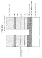
- the semiconductor thin film is brought into an intimate contact with the metal layer/metal-oxide layer by means of moisture for Van der Waals Bonding (VDWB). Then, the etching mask 311 on the semiconductor thin film is removed (Fig. 3E).
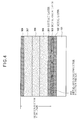
- Fig. 4 is a model representation of the semiconductor thin film illustrating the vicinity of the bonded interface between the metal layer and metal oxide layer after the device in Fig. 3E is further sintered at a temperature of 200°C for 1 hour.
- Sintering is performed at a temperature lower than the melting point of the metal oxide layer 103.
- the sintering for Au is performed at a temperature lower than 1064°C.
- the sintering is performed for a time length and at a temperature such that oxide molecules or oxygen atoms in chemical combination with the metal can diffuse into the metal. Referring to Fig.
- a surface oxide portion of a metal layer 102 diffuses into the metal oxide layer 103 formed between the contact layer 304 of the semiconductor thin film and the metal layer 102, and into an oxide layer on the surface oxide portion of the contact layer 304, thereby forming a metal/semiconductor reaction region 410.
- This not only provides reliable bonding between the semiconductor thin film and the metal layer but also establishes good electrical contact of a low resistance between the semiconductor thin film and the metal layer.
- an oxide layer is formed on the surface of the metal layer. This allows using of moisture between the semiconductor thin film and the metal layer for improving intimate contact of the semiconductor thin film with the metal layer. This offers excellent bonding strength.
- the provision of a metal oxide layer is effective in easing the reaction between the metal and the contact layer (i.e., bonding layer) of the semiconductor thin film so that voids produced during the reaction can be minimized for reliable bonding interface.
- the first embodiment has been described with respect to an Si substrate as a semiconductor substrate.
- the semiconductor substrate may also be a semiconductor substrate such as a GaAs substrate, an insulating substrate such as a ceramic substrate and a glass substrate, or an electrically conductive substrate made of metals such as copper, stainless steel, or aluminum.
- a metal substrate is to be employed, this can eliminate the need for forming a metal layer on the metal substrate and oxidizing the metal layer. That is, a roughness on the order of nano meters can be formed on the surface of the substrate and the rough surface can then be oxidized
- Fig. 5 illustrates a second embodiment.
- a substrate 101 is, for example, an Si substrate.
- a metal layer 102 is formed on the Si substrate 101.
- an oxide layer 103 of the metal layer 102 is formed on the metal layer 102.
- a metal layer 501 is formed under a contact layer of a semiconductor thin film 104.
- a metal oxide layer 502 is formed under the metal layer 501.
- the second embodiment differs from the first embodiment in that a metal layer/metal-oxide layer is formed on the semiconductor thin film 104 side as well.
- the metal layer 501 may be a metal layer that contains Pd, Au, Ge, Ni, Pt, or Ti, an Ni layer, or a metal layer that contains Au and is covered with a Pd layer or a Ni layer.
- the metal oxide layer 502 may be formed, for example, by means of oxygen plasma.
- the thickness of the metal oxide layer 502 is preferably in the range of 1 to 10 nm if electrical contact is to be formed in the vicinity of the bonded interface between the semiconductor thin film and the metal layer.
- Fig. 6 illustrates the reaction that takes place in the vicinity of the bonded interface after sintering the structure in Fig. 5 at a temperature of 200°C for 1 hour.
- a metal diffuses into a metal oxide layer 103 and a metal oxide layer 502 to form a metal-and-metal reaction region 610, i.e., a metal-and-metal oxide layer.
- a metal/metal-oxide layer is formed on the semiconductor thin film side as well. This offers a highly intimate junction interface so that a further lower contact resistance can be implemented between the semiconductor thin film and the metal layer. Because both substrate and the semiconductor thin film supply metal materials, the metal can diffuse into the metal oxide layer sufficiently, thereby resulting in a highly strong bonding without voids.
- Fig. 7 illustrates a third embodiment.
- the third embodiment differs from the first embodiment in that a metal layer 501 and a metal oxide layer 502 are formed on a semiconductor thin film 104 side.
- a substrate 101 in Fig. 7 is an Si substrate.
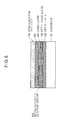
- Fig. 8 is a model representation illustrating the vicinity of the bonded interface after sintering the structure in Fig. 7 at a temperature of 500°C for 10 minutes. It is to be noted that a metal layer 501 has diffused into an oxide layer 502 to form a metal compound 710 between the Si substrate 101 and the metal layer 501.
- the metal layer 501 and the metal oxide layer 502 are formed on the semiconductor thin film 104 side.
- This structure allows the device to be sintered at a higher temperature, resulting in a lower contact resistance between the semiconductor thin film 104 and the metal layer 501 as well as forming a silicide between the metal layer 501 and the Si substrate 101 for good bonding effect.
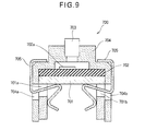
- Fig. 9 is a side cross-sectional view of an LED head on which a semiconductor device according to the present invention is mounted.
- an LED head 700 includes a base member 701 and an LED unit 702 that is fixedly mounted on the base member 701.
- the LED unit 702 employs any one of various LED/driver composite chips according to the first to third embodiments.
- a light-emitting section 702a is formed on the previously mentioned semiconductor epitaxial layer, and includes a number of light-emitting elements aligned in line.
- a rod lens array 703 extends over the light-emitting section 702a and focuses the light emitted from the light-emitting section 702a on a surface of an appropriate external member.
- the rod lens array 703 includes a plurality of rod-like optical lenses aligned along the line of light-emitting elements.
- a lens holder 104 holds the rod lens array 103 in position.
- the lens holder 704 is formed to enclose the base member 701 and LED unit 702.
- Clampers 705 extend through openings 701a, 701b, 704a, and 704b, and hold the base member 701, LED unit 702, and lens holder 704 firmly in a stacked relation.
- the light emitted from the light-emitting section 702a passes the rod lens array 703 and illuminates the surface of the appropriate external member.
- the LED head 700 is used as a photolithography machine in electrophotographic image forming apparatuses and electrophotographic copying machines.
- the aforementioned LED head 700 uses one of the LED/driver IC composite chips described in the previous embodiments and therefore provides a compact, high-quality, and cost-saving LED head.
- Fig. 10 illustrates an image forming apparatus 200 incorporating an LED head that employs a semiconductor composite device according to the present invention.
- the image forming apparatus 200 includes process units 201-204 that form yellow, magenta, cyan, and black images.
- the process units 201-204 are aligned in this order from an upstream side of a transport path for a recording medium to a downstream side.
- Each of the process units 201-204 may be substantially identical; for simplicity only the operation of the process unit 203 will be described, it being understood that the other process units may work in a similar fashion.
- the process unit 203 includes a photoconductive drum 203a that rotates in a direction shown by arrow C.
- a charging unit 203b, exposing unit 203c, developing unit 203d, and cleaning unit 203e are disposed to surround the photoconductive drum 203a, being aligned from an upstream side to a downstream side with respect to a direction of rotation of the photoconductive drum 203a.
- the charging unit 203b charges the surface of the photoconductive drum 203a.
- the exposing unit 203c illuminates the charged surface of the photoconductive drum 203a to form an electrostatic latent image.
- the developing unit 203d supplies toner to the electrostatic latent image to develop the electrostatic latent image into a toner image.
- the cleaning unit 203e removes the toner remaining on the photoconductive drum 203a after transferring the toner image onto a recording medium 205.
- Drums or rollers used in these units are driven in rotation by a drive source, not shown, via a gear train.
- a paper cassette 206 is provided at a lower portion of the image forming apparatus 200, and holds a stack of the recording medium 205 such as paper therein.
- a hopping roller 207 is disposed over the paper cassette 206 and feeds the recording medium 205 on a page-by-page basis to the transport path.
- the pinch rollers 208 and 209 and the transporting roller 210 hold the recording medium 205 in a sandwiched relation and transport the recording medium 205.
- the registry roller 211 minimizes skew between the recording medium 205 and the transport path and then transports the recording medium 205 to the process unit 201.
- the hopping roller 207, transporting roller 210, and registry roller 211 are driven in rotation by a drive source, not shown, via, for example, a gear train.
- Transfer rollers 212 are formed of a semi conductive rubber and are provided to oppose the photoconductive drums of the process units 201-204.
- the transfer roller 212 receives a high voltage for transferring a toner image from the surface of the photoconductive drum 203a to the recording medium 205.
- a fixing unit 213 includes a heat roller and a back-up roller so that the toner image on the recording medium 205 is fused into a permanent image under heat and pressure.
- Discharging rollers 214 and 215 cooperate with the pinch rollers 216 and 217 to hold the recording medium 205 in a sandwiched relation and transport the recording medium 205 to a stacker.
- the fixing units 213 and discharging roller 214 are driven in rotation by a drive source, not shown, via, for example, a gear train.
- the exposing unit 203c takes the form of the aforementioned LED head.
- the operation of the aforementioned image forming apparatus 200 will be described.
- the hopping roller 207 feeds the recording medium 205 on a page-by-page basis. Then, the recording medium 205 is held between the transporting roller 210, registry roller 211 and pinch rollers 208 and 209 in a sandwiched relation, and is transported to the process unit 201.
- the recording medium 205 is pulled in between the photoconductive drum 201a and the transfer roller 212 so that the toner image is transferred onto the recording medium 205 as the recording medium 205 is advanced between the photoconductive drum 201a and the transfer roller 212.
- the recording medium 205 passes through the process units 201-204.
- the exposing units 201c-204c form electrostatic latent images of corresponding colors and the developing units 201d-204d develop the corresponding electrostatic latent images to form toner images of the corresponding colors.
- the toner images of corresponding colors are transferred onto the recording medium in registration.
- the recording medium 205 then enters the fixing unit 213 where the toner images are fixed into a full color permanent image. Then, the recording medium 205 is held between the discharging rollers 214 and 215 and the pinch rollers 216 and 217 in a sandwiched relation so that the recording medium 205 is discharged to the stacker 218.
Landscapes
- Physics & Mathematics (AREA)
- Optics & Photonics (AREA)
- Health & Medical Sciences (AREA)
- General Health & Medical Sciences (AREA)
- Toxicology (AREA)
- Printers Or Recording Devices Using Electromagnetic And Radiation Means (AREA)
- Led Device Packages (AREA)
- Led Devices (AREA)
Abstract
Description
- The present invention relates to a semiconductor composite device, a method for manufacturing the semiconductor composite device, an LED head that employs the semiconductor composite device, and an image forming apparatus that employs the LED head.
-
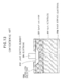
- Fig. 11 is a perspective view of a conventional light-emitting diode (LED)
unit 2000 on which LED chips are mounted. - Fig. 12 is a top view illustrating a part of an
LED chip 2001. - Fig. 13 is a cross-sectional view taken along a line A-A of Fig. 12.
- Referring to Fig. 11, the
LED unit 2000 includes primarily a plurality ofLED chips 2001, a plurality ofdriver IC chips 2002,wires 2003 that connect between theLED chips 2001 anddriver IC chips 2002, and aunit substrate 2005. Referring to Fig. 12, theLED chip 2001 includeslight emitting elements 2101, electrodes2102 for light-emittingelements 2101, andelectrode pads 2103 for wiring. Theelectrode pads 2103 should have a sufficient area for reliable gold-wire bonding. Therefore, the pad size is selected to be about 100×100 µm. The cost of a chip is determined by the number of chips produced from a sheet of semiconductor wafer. Thus, a small chip width is a key factor. There exists a need for a semiconductor device such as an LED chip and an IC chip where pads take up only a small area and wire bonding is not required. - One way of solving the aforementioned problems is that a semiconductor thin film is bonded onto an Si-substrate in which driver ICs are formed for controllably driving light-emitting elements and the semiconductor thin film is electrically connected to the driver ICs by means of metal wires. In this case, a critical point is the way in which the semiconductor thin film is bonded onto a substrate which is a different type from the semiconductor thin film.
- For a type in which the light-emitting chips are bonded to an Si-substrate on which driver ICs are fabricated, a semiconductor thin film may be conveniently bonded to a metal layer formed on the Si-substrate. For a type where a semiconductor thin film is bonded to a substrate of a different type from the thin film semiconductor, a bonding method may be conveniently employed which utilizes Van der Waals forces that act between atoms or molecules of the semiconductor thin film and the substrate of the different type from the thin film semiconductor. However, for bonding based on the Van der Waals forces, surfaces of the semiconductor thin film and substrate are made hydrophilic and are then placed together so that the surfaces are bonded to each other due to hydrogen bonding. However, metal surfaces are often hydrophobic and therefore it has not been known what type of surface type is the most appropriate.
- An object of the present invention is to provide a bonding that provides good, reliable bonding properties by using the Van der Waals forces between the semiconductor surface and metal surface.
- A semiconductor composite apparatus includes a semiconductor thin film (104), a substrate (101), and a region (102, 103) . The substrate (101) includes a metal surface (102) to which the semiconductor thin film (104) is bonded. The region (102, 103) contains an oxide (103) of a metal that forms the metal surface (102). The region (102, 103) lies between the semiconductor thin film (104) and the metal surface (101).
- The metal surface (102) is a surface of a metal layer (102) provided on the substrate (101).
- The metal surface (501) contains an element selected from the group consisting of Pd, Ni, Ge, Pt, Ti, Cr, and Au.
- The metal layer is either a surface of a Pd layer or a surface of an Ni layer. A semiconductor composite apparatus includes a substrate and a semiconductor thin film bonded to the substrate. A first metal layer (501) is formed on a surface of the semiconductor thin film (104), the surface of the semiconductor thin film (104) facing the substrate (101) . A metal surface (102) is formed on a surface of the substrate (101), surface of the substrate (101) facing the semiconductor thin film (104) . A region lying (610) is formed between the first metal layer (501) and the metal surface (102) . The region contains an oxide (502) of a metal element that forms the first metal layer (501) and an oxide (103) of a metal element that forms the metal surface (102).
- The metal surface (102) is either a Pd layer or an Ni layer. The metal surface (102) contains an element selected from the group consisting of Pd, Ni, Ge, Pt, Ti, Cr, and Au.
- The metal surface (102) is either surface of a Pd layer or a surface of an Ni layer.
- A semiconductor composite apparatus includes a semiconductor thin film (104) separated from a first substrate and then bonded to a second substrate (101) . The apparatus includes a first metal layer (501) and a region (710). The first metal layer (501) is formed on a surface of the semiconductor thin film (104), the first metal layer (501) facing the second substrate (101). The region (710) contains an oxide of a metal that forms the first metal layer (501), the region (710) lying between the first metal layer (501) and a surface of the second substrate (101).
- The first metal layer (501) contains an element selected from the group consisting of Pd, Ni, Ge, Pt, Ti, Cr, and Au.
- The first metal layer (501) is coated with either a Pd layer or an Ni layer.
- The semiconductor thin film (104) includes at least one of a light-emitting element, a light-receiving element, a transistor, a circuit element, and an integrated circuit.
- The light-emitting element may be a light emitting diode (LED) .
- The light-emitting diode may be a laser diode (LD).
- An LED head incorporates the aforementioned semiconductor composite apparatus.
- An LED head incorporates the semiconductor composite apparatus. An optical device (103) that adjusts light emitted from the semiconductor composite apparatus.
- An image forming apparatus incorporates the LED head. A photoconductive body (201a-204a) is illuminated by the LED head (100) .
- A method is used for manufacturing a semiconductor composite apparatus in which a semiconductor thin film is separated from a first substrate and is bonded to a second substrate including a metal layer formed thereon. The method includes the steps of:
- bringing the semiconductor thin film (104) into contact with the metal layer formed on the second substrate (101); and
- forming a region that contains an oxide of a metal element of the metal layer, the region lying between the semiconductor thin film and the metal layer.
- A method is used for manufacturing a semiconductor composite apparatus in which a semiconductor thin film is separated from a first substrate and is bonded to a second substrate. The method includes the steps of:
- forming a first metal layer (501) on a surface of the semiconductor thin film (104), the surface facing the second substrate (101);
- forming a second metal layer on the second substrate (101), the second metal layer facing the semiconductor thin film (104) ; and
- forming a region (610) that contains an oxide (502) of a metal element of the first metal layer (501) and an oxide (103) of a metal element of a second metal layer (102), the region (610) lying between the first metal layer (501) and the second metal layer (102).
- A method is used for manufacturing a semiconductor composite apparatus in which a semiconductor thin film is separated from a first substrate and is bonded to a second substrate. The method includes the steps of:
- forming a first metal layer (501) on a surface of the semiconductor thin film (104), the surface facing the second substrate (101); and
- forming a region (710) that contains an oxide of a metal element of the first metal layer (501), the region (710) lying between the first metal layer (501) and a surface of the second substrate (101).
- A method is used for manufacturing a semiconductor composite apparatus. The method includes the steps of:
- forming a metal layer (501 or 102) on at least one of a semiconductor thin film (104) and a substrate (101);
- forming a metal oxide (502 or 103) of an element of the metal layer (501 or 102); and
- forming a layer of water on the metal oxide (502 or 103) and bringing the semiconductor thin film (104) into intimate contact with the substrate (101) with the layer of water lying between the semiconductor thin film (104) and the substrate (101).
- Further scope of applicability of the present invention will become apparent from the detailed description given hereinafter. However, it should be understood that the detailed description and specific examples, while indicating preferred embodiments of the invention, are given by way of illustration only, since various changes and modifications within the spirit and scope of the invention will become apparent to those skilled in the art from this detailed description.
- The present invention will become more fully understood from the detailed description given hereinbelow and the accompanying drawings which are given by way of illustration only, and thus are not limiting the present invention, and wherein:
- Fig. 1 is a model representation illustrating a first embodiment of the invention;
- Fig. 2 illustrates an example of a semiconductor thin film detached from a second substrate;
- Figs. 3A-3E illustrate the steps of forming a semiconductor thin film;
- Fig. 4 is a model representation of the semiconductor thin film and the vicinity of a bonded interface between a metal layer and a metal oxide layer after the device in Fig. 3E is sintered;
- Fig. 5 illustrates a second embodiment;
- Fig. 6 illustrates a reaction in the vicinity of the bonded interface after sintering the structure in Fig. 5;
- Fig. 7 illustrates a third embodiment;
- Fig. 8 is a model representation of the vicinity of a bonded interface after sintering the structure in Fig. 7;
- Fig. 9 is a side cross-sectional view of an LED head on which a semiconductor device according to the present invention is mounted;
- Fig. 10 illustrates an image forming apparatus incorporating an LED head that employs a semiconductor composite device according to the present invention;
- Fig. 11 is a perspective view of a conventional light-emitting diode (LED) unit on which LED chips are mounted;
- Fig. 12 is a top view illustrating a part of an LED chip of Fig. 11; and
- Fig. 13 is a cross-sectional view taken along a line A-A of Fig. 12.
- Fig. 1 is a model representation illustrating a first embodiment of the invention. Referring to Fig. 1, a
substrate 101 is, for example, an Si substrate. Ametal layer 102 is formed on thesubstrate 101. Themetal layer 102 is of a single metal layer structure or a multi-metal layer structure. Anoxide layer 103 includes an oxide layer that contains the element of themetal layer 102 and the element of a semiconductorthin film 104. The semiconductorthin film 104 is a thin layer of compound semiconductor that is formed of III-V groups of periodic table and is a single layer of semiconductor epitaxial layer or multi-layers of semiconductor epitaxial layer. Theoxide layer 103 contains a metal oxide layer that contains the metal element of themetal layer 102, the metal oxide layer facing themetal layer 102. Theoxide layer 103 contains an oxide layer that contains elements that form the semiconductorthin film 104, theoxide layer 103 facing the semiconductorthin film 104. - Fig. 2 illustrates an example of another semiconductor
thin film 104 transferred from another substrate. Afirst contact layer 201 is for example, an n-type layer of GaAs. A first cladlayer 202 is, for example, an n-type layer of AlxGa1-xAs. Anactive layer 203 is, for example, an n-type layer of AlyGA1-yAs. A second cladlayer 204 is, for example, a p-type layer of AlzGa1-zAs. Asecond contact layer 205 is, for example, a p-type layer of GaAs. The variables x, y, and z are related such that 1≧x and z>y≧0. - Figs. 3A-3E illustrate the steps of forming still another semiconductor thin film that includes the
layers 304 to 308. Referring to Fig. 3A, asubstrate 301 is, for example, a GaAs substrate. Abuffer layer 302 is, for example, a GaAs buffer layer. Arelease layer 303 is, for example, an AlAs layer. Therelease layer 303 can be etched selectively independently from the semiconductorthin film 104 while the semiconductorthin film 104 can be etched selectively independently from therelease layer 303. The semiconductorthin film 104 includes at least one of a light-emitting element, a light-receiving element, a transistor, circuit element, and an integrated circuit. - Referring to Fig. 3B, the
etching mask 311 is formed on the semiconductor epitaxial substrate and a mesa-etch groove 312 is formed to divide the semiconductor thin film into a plurality of individual regions. The mesa-etch groove 312 has a depth such that at least therelease layer 303 is exposed. Subsequently, therelease layer 303 is etched to separate the individual regions (i.e. , individual layers of semiconductor thin films 104) from the rest as shown in Fig. 3C. An etchant for this process may be, for example, 10%-hydrogen fluoride (HF) . Alternatively, acids may be used that can etch a layer of semiconductor thin film and the release layer independently. After etching, an individual region is bonded to another substrate, e.g. , an Si-substrate on which themetal layer 102 and themetal oxide layer 103 are formed (Fig. 3D). - The
metal layer 102 may be a single layer of Pd, a single layer of Ni, or a metal layer such as a single layer, a multi-layer, or an alloy layer that contains at least one of Au, Ge, Pt, Ti, and Cr. Themetal layer 102 may also be an Au-containing metal layer coated with a Pd layer or an Au-containing metal layer coated with an Ni layer. Au is highly resistant to oxidation. Thus, if themetal layer 102 is made of Au, a very thin oxide film (e.g., 3 to 5 nm thick), a very thin Au film (e.g., 3 to 5 nm thick) that has attracted oxygen, or a composite layer of these films is formed. The surface of themetal layer 102 is exposed to oxygen plasma to form a very thin metal oxide layer on the surface of the metal layer. When the surface of a metal layer is covered with a metal, the surface is hydrophobic, i.e., the surface repels water. However, because a thin oxide layer is formed on the outermost surface of the metal, the surface is hydrophilic. This allows preparing of the semiconductor thin film that can be intimately attached to the bonding region. It is considered that oxygen atoms are highly hydrophilic and therefore oxygen atoms on the surface of the metal oxide attract water molecules. In addition to the aforementioned metals, aluminum may be used to form the metal layer. However, the surface of aluminum is difficult to be flat, and therefore conditions for making films may be preferably altered so that the resultant aluminum surface can be flat or themetal layer 102 is subjected to a surface-flattening treatment after the film is formed. - The
metal oxide layer 103 may have any thickness. For example, in order to provide good electrical contact between the semiconductor thin film and the metal layer, the thickness is preferably in the range of 1 to 10 nm. Following are the reasons. For establishing a good electrical contact between the back side of the semiconductor thin film and the metal layer, sintering is performed after bonding the semiconductor thin film so that the atoms in the vicinity of the interface between the semiconductor thin film and the metal layer are interdiffused and/or intermixed, and alloyed. Sintering is performed at a temperature in the range of 100 to 400°C for a time length in the range of 0.5 to 5 hours. If theoxide layer 103 is thick, atoms of the semiconductor thin film and the metal layer will not pass through the oxide layer. In other words, the semiconductor thin film and the metal layer will not react with each other, failing to form a low resistance contact. - Subsequently, the semiconductor thin film is brought into an intimate contact with the metal layer/metal-oxide layer by means of moisture for Van der Waals Bonding (VDWB). Then, the
etching mask 311 on the semiconductor thin film is removed (Fig. 3E). - Fig. 4 is a model representation of the semiconductor thin film illustrating the vicinity of the bonded interface between the metal layer and metal oxide layer after the device in Fig. 3E is further sintered at a temperature of 200°C for 1 hour. Sintering is performed at a temperature lower than the melting point of the
metal oxide layer 103. For example, the sintering for Au is performed at a temperature lower than 1064°C. In other words, the sintering is performed for a time length and at a temperature such that oxide molecules or oxygen atoms in chemical combination with the metal can diffuse into the metal. Referring to Fig. 4, a surface oxide portion of ametal layer 102 diffuses into themetal oxide layer 103 formed between thecontact layer 304 of the semiconductor thin film and themetal layer 102, and into an oxide layer on the surface oxide portion of thecontact layer 304, thereby forming a metal/semiconductor reaction region 410. This not only provides reliable bonding between the semiconductor thin film and the metal layer but also establishes good electrical contact of a low resistance between the semiconductor thin film and the metal layer. - According to the first embodiment, when a semiconductor thin film is to be bonded on a substrate of different material with a metal layer positioned between the semiconductor thin film and the substrate, an oxide layer is formed on the surface of the metal layer. This allows using of moisture between the semiconductor thin film and the metal layer for improving intimate contact of the semiconductor thin film with the metal layer. This offers excellent bonding strength. The provision of a metal oxide layer is effective in easing the reaction between the metal and the contact layer (i.e., bonding layer) of the semiconductor thin film so that voids produced during the reaction can be minimized for reliable bonding interface. The first embodiment has been described with respect to an Si substrate as a semiconductor substrate. The semiconductor substrate may also be a semiconductor substrate such as a GaAs substrate, an insulating substrate such as a ceramic substrate and a glass substrate, or an electrically conductive substrate made of metals such as copper, stainless steel, or aluminum. When a metal substrate is to be employed, this can eliminate the need for forming a metal layer on the metal substrate and oxidizing the metal layer. That is, a roughness on the order of nano meters can be formed on the surface of the substrate and the rough surface can then be oxidized
- Fig. 5 illustrates a second embodiment. A
substrate 101 is, for example, an Si substrate. Ametal layer 102 is formed on theSi substrate 101. Then, anoxide layer 103 of themetal layer 102 is formed on themetal layer 102. Ametal layer 501 is formed under a contact layer of a semiconductorthin film 104. Ametal oxide layer 502 is formed under themetal layer 501. The second embodiment differs from the first embodiment in that a metal layer/metal-oxide layer is formed on the semiconductorthin film 104 side as well. - The
metal layer 501 may be a metal layer that contains Pd, Au, Ge, Ni, Pt, or Ti, an Ni layer, or a metal layer that contains Au and is covered with a Pd layer or a Ni layer. Just as in the first embodiment, themetal oxide layer 502 may be formed, for example, by means of oxygen plasma. The thickness of themetal oxide layer 502 is preferably in the range of 1 to 10 nm if electrical contact is to be formed in the vicinity of the bonded interface between the semiconductor thin film and the metal layer. - Fig. 6 illustrates the reaction that takes place in the vicinity of the bonded interface after sintering the structure in Fig. 5 at a temperature of 200°C for 1 hour. Referring to Fig. 6, a metal diffuses into a
metal oxide layer 103 and ametal oxide layer 502 to form a metal-and-metal reaction region 610, i.e., a metal-and-metal oxide layer. - According to the second embodiment, in addition to the structure according to the first embodiment, a metal/metal-oxide layer is formed on the semiconductor thin film side as well. This offers a highly intimate junction interface so that a further lower contact resistance can be implemented between the semiconductor thin film and the metal layer. Because both substrate and the semiconductor thin film supply metal materials, the metal can diffuse into the metal oxide layer sufficiently, thereby resulting in a highly strong bonding without voids.
- Fig. 7 illustrates a third embodiment. The third embodiment differs from the first embodiment in that a
metal layer 501 and ametal oxide layer 502 are formed on a semiconductorthin film 104 side. Asubstrate 101 in Fig. 7 is an Si substrate. Fig. 8 is a model representation illustrating the vicinity of the bonded interface after sintering the structure in Fig. 7 at a temperature of 500°C for 10 minutes. It is to be noted that ametal layer 501 has diffused into anoxide layer 502 to form ametal compound 710 between theSi substrate 101 and themetal layer 501. - According to the third embodiment, the
metal layer 501 and themetal oxide layer 502 are formed on the semiconductorthin film 104 side. This structure allows the device to be sintered at a higher temperature, resulting in a lower contact resistance between the semiconductorthin film 104 and themetal layer 501 as well as forming a silicide between themetal layer 501 and theSi substrate 101 for good bonding effect. - Fig. 9 is a side cross-sectional view of an LED head on which a semiconductor device according to the present invention is mounted. Referring to Fig. 9, an
LED head 700 includes abase member 701 and anLED unit 702 that is fixedly mounted on thebase member 701. TheLED unit 702 employs any one of various LED/driver composite chips according to the first to third embodiments. A light-emittingsection 702a is formed on the previously mentioned semiconductor epitaxial layer, and includes a number of light-emitting elements aligned in line. Arod lens array 703 extends over the light-emittingsection 702a and focuses the light emitted from the light-emittingsection 702a on a surface of an appropriate external member. Therod lens array 703 includes a plurality of rod-like optical lenses aligned along the line of light-emitting elements. Alens holder 104 holds therod lens array 103 in position. - The
lens holder 704 is formed to enclose thebase member 701 andLED unit 702.Clampers 705 extend throughopenings base member 701,LED unit 702, andlens holder 704 firmly in a stacked relation. - The light emitted from the light-emitting
section 702a passes therod lens array 703 and illuminates the surface of the appropriate external member. TheLED head 700 is used as a photolithography machine in electrophotographic image forming apparatuses and electrophotographic copying machines. - The
aforementioned LED head 700 uses one of the LED/driver IC composite chips described in the previous embodiments and therefore provides a compact, high-quality, and cost-saving LED head. - Fig. 10 illustrates an
image forming apparatus 200 incorporating an LED head that employs a semiconductor composite device according to the present invention. Referring to Fig. 10, theimage forming apparatus 200 includes process units 201-204 that form yellow, magenta, cyan, and black images. The process units 201-204 are aligned in this order from an upstream side of a transport path for a recording medium to a downstream side. Each of the process units 201-204 may be substantially identical; for simplicity only the operation of theprocess unit 203 will be described, it being understood that the other process units may work in a similar fashion. - The
process unit 203 includes aphotoconductive drum 203a that rotates in a direction shown by arrow C. A chargingunit 203b, exposingunit 203c, developingunit 203d, andcleaning unit 203e are disposed to surround thephotoconductive drum 203a, being aligned from an upstream side to a downstream side with respect to a direction of rotation of thephotoconductive drum 203a. The chargingunit 203b charges the surface of thephotoconductive drum 203a. The exposingunit 203c illuminates the charged surface of thephotoconductive drum 203a to form an electrostatic latent image. The developingunit 203d supplies toner to the electrostatic latent image to develop the electrostatic latent image into a toner image. Thecleaning unit 203e removes the toner remaining on thephotoconductive drum 203a after transferring the toner image onto arecording medium 205. Drums or rollers used in these units are driven in rotation by a drive source, not shown, via a gear train. - A
paper cassette 206 is provided at a lower portion of theimage forming apparatus 200, and holds a stack of therecording medium 205 such as paper therein. A hoppingroller 207 is disposed over thepaper cassette 206 and feeds therecording medium 205 on a page-by-page basis to the transport path. There are providedpinch rollers roller 210, and aregistry roller 211 in the transport path downstream of the hoppingroller 207. Thepinch rollers roller 210 hold therecording medium 205 in a sandwiched relation and transport therecording medium 205. Theregistry roller 211 minimizes skew between therecording medium 205 and the transport path and then transports therecording medium 205 to theprocess unit 201. The hoppingroller 207, transportingroller 210, andregistry roller 211 are driven in rotation by a drive source, not shown, via, for example, a gear train. -
Transfer rollers 212 are formed of a semi conductive rubber and are provided to oppose the photoconductive drums of the process units 201-204. Thetransfer roller 212 receives a high voltage for transferring a toner image from the surface of thephotoconductive drum 203a to therecording medium 205. - A fixing
unit 213 includes a heat roller and a back-up roller so that the toner image on therecording medium 205 is fused into a permanent image under heat and pressure. Dischargingrollers pinch rollers recording medium 205 in a sandwiched relation and transport therecording medium 205 to a stacker. The fixingunits 213 and dischargingroller 214 are driven in rotation by a drive source, not shown, via, for example, a gear train. The exposingunit 203c takes the form of the aforementioned LED head. - The operation of the aforementioned
image forming apparatus 200 will be described. The hoppingroller 207 feeds therecording medium 205 on a page-by-page basis. Then, therecording medium 205 is held between the transportingroller 210,registry roller 211 andpinch rollers process unit 201. Therecording medium 205 is pulled in between the photoconductive drum 201a and thetransfer roller 212 so that the toner image is transferred onto therecording medium 205 as therecording medium 205 is advanced between the photoconductive drum 201a and thetransfer roller 212. - The
recording medium 205 passes through the process units 201-204. The exposing units 201c-204c form electrostatic latent images of corresponding colors and the developing units 201d-204d develop the corresponding electrostatic latent images to form toner images of the corresponding colors. As therecording medium 205 passes through the process units 201d-204d, the toner images of corresponding colors are transferred onto the recording medium in registration. Therecording medium 205 then enters the fixingunit 213 where the toner images are fixed into a full color permanent image. Then, therecording medium 205 is held between the dischargingrollers pinch rollers recording medium 205 is discharged to thestacker 218. - The invention being thus described, it will be obvious that the same may be varied in many ways. Such variations are not to be regarded as a departure from the spirit and scope of the invention, and all such modifications as would be obvious to one skilled in the art intended to be included within the scope of the following claims.
Claims (21)
- A semiconductor composite apparatus, comprising:a semiconductor thin film (104);a substrate (101) including a metal surface (102) to which said semiconductor thin film (104) is bonded; anda region (102, 103) that contains an oxide (103) of a metal that forms the metal surface (102), said region (102, 103) lying between said semiconductor thin film 104) and said metal surface (101) .
- The semiconductor composite apparatus according to Claim 1, wherein the metal surface (102) is a surface of a metal layer (102) provided on said substrate (101).
- The semiconductor composite apparatus according to Claim 1 or 2 , wherein the metal surface (501) contains an element selected from the group consisting of Pd, Ni, Ge, Pt, Ti, Cr, and Au.
- The semiconductor composite apparatus according to Claim 2 Or 3, wherein the metal layer (102) is either a surface of a Pd layer or a surface of an Ni layer.
- A semiconductor composite apparatus in which a semiconductor thin film (104) is bonded to a substrate (101), the apparatus comprising:a first metal layer(501) formed on a surface of the semiconductor thin film (104), the surface of the semiconductor thin film (104) facing the substrate (101);a metal surface (102) formed on a surface of the substrate (101), the surface of the substrate (101) facing the semiconductor thin film (104);a region lying (610) between said first metal layer (501) and said metal surface (102), said region (610) containing an oxide (502) of a metal element that forms said first metal layer (501) and an oxide (103) of a metal element that forms said metal surface (102) .
- The semiconductor composite apparatus according to Claim 5, wherein said metal surface (102) is either a Pd layer or an Ni layer.
- The semiconductor composite apparatus according to Claim 5 or 6, wherein the metal surface (102) contains an element selected from the group consisting of Pd, Ni, Ge, Pt, Ti, Cr, and Au.
- The semiconductor composite apparatus according to any of Claims 5 to 7, wherein the metal surface (102) is either a surface of a Pd layer or a surface of an Ni layer.
- A semiconductor composite apparatus in which a semiconductor thin film (104) is separated from a first substrate and is then bonded to a second substrate (101), the apparatus comprising:a first metal layer (501) formed on a surface of the semiconductor thin film (104), said first metal layer (501) facing the second substrate (101);a region (710) that contains an oxide (710) of a metal that forms the first metal layer (501), said region (710) lying between said first metal layer (501) and a surface of the second substrate (101) .
- The semiconductor according to Claim 9, wherein the first metal layer (501) contains an element selected from the group consisting of Pd, Ni, Ge, Pt, Ti, Cr, and Au.
- The semiconductor composite apparatus according to Claim 9 or 10, wherein the first metal layer (501) is coated with either a Pd layer or an Ni layer.
- The semiconductor composite apparatus according to Claim 1 wherein the semiconductor thin film (104) includes at least one of a light-emitting element, a light-receiving element, a transistor, a circuit element, and an integrated circuit.
- The semiconductor composite apparatus according to Claim 12, wherein the light-emitting element is a light emitting diode (LED) .
- The semiconductor composite apparatus according to Claim 12, wherein the light-emitting diode is a laser diode (LD).
- An LED head incorporating said semiconductor composite apparatus according to Claim 1.
- An LED head incorporating said semiconductor composite apparatus according to Claim 13, comprising:an optical device (103) that adjusts light emitted from said semiconductor composite apparatus.
- An image forming apparatus incorporating said LED head according to Claim 12, comprising:a photoconductive body (201a-204a) that is illuminated by said LED head (100).
- A method for manufacturing a semiconductor composite apparatus in which a semiconductor thin film is separated from a first substrate and is bonded to a second substrate including a metal layer formed thereon, the method comprising the steps of:bringing the semiconductor thin film (104) into contact with the metal layer formed on the second substrate (101); andforming a region that contains an oxide of a metal element of the metal layer, the region lying between the semiconductor thin film and the metal layer.
- A method for manufacturing a semiconductor composite apparatus in which a semiconductor thin film is separated from a first substrate and is bonded to a second substrate (101), the method comprising the steps of:forming a first metal layer (501) on a surface of the semiconductor thin film (104), the surface facing the second substrate (101);forming a second metal layer on the second substrate (101), the second metal layer facing the semiconductor thin film (104) ; andforming a region (610) that contains an oxide (502) of a metal element of the first metal layer (501) and an oxide (103) of a metal element of a second metal layer (102), the region (610) lying between the first metal layer (501) and the second metal layer (102).
- A method for manufacturing a semiconductor composite apparatus in which a semiconductor thin film is separated from a first substrate and is bonded to a second substrate, the method comprising the steps of:forming a first metal layer (501) on a surface of the semiconductor thin film (104), the surface facing the second substrate (101); andforming a region (710) that contains an oxide of a metal element of the first metal layer (501), the region (710) lying between the first metal layer (501) and a surface of the second substrate (101).
- A method for manufacturing a semiconductor composite apparatus, the method comprising the steps of:forming a metal layer (501 or 102) on at least one of a semiconductor thin film (104) and a substrate (101);forming a metal oxide (502 or 103) of an element of the metal layer (501 or 102); andforming a layer of water on a surface of the metal oxide (502 or 103) and bringing the semiconductor thin film (104) into intimate contact with the substrate (101) with the layer of water lying between the semiconductor thin film (104) and the substrate (101) .
Applications Claiming Priority (1)
| Application Number | Priority Date | Filing Date | Title |
|---|---|---|---|
| JP2004266834A JP2006082260A (en) | 2004-09-14 | 2004-09-14 | Semiconductor composite device, method for manufacturing semiconductor composite device, LED head using semiconductor composite device, and image forming apparatus using this LED head |
Publications (3)
| Publication Number | Publication Date |
|---|---|
| EP1635404A2 true EP1635404A2 (en) | 2006-03-15 |
| EP1635404A3 EP1635404A3 (en) | 2011-03-09 |
| EP1635404B1 EP1635404B1 (en) | 2014-01-08 |
Family
ID=35457561
Family Applications (1)
| Application Number | Title | Priority Date | Filing Date |
|---|---|---|---|
| EP05108378.0A Ceased EP1635404B1 (en) | 2004-09-14 | 2005-09-13 | Semiconductor composite device, method for manufacturing the semiconductor composite device, LED head that employs the semiconductor composite device, and image forming apparatus that employs the LED head |
Country Status (4)
| Country | Link |
|---|---|
| US (2) | US7432523B2 (en) |
| EP (1) | EP1635404B1 (en) |
| JP (1) | JP2006082260A (en) |
| CN (1) | CN1750255B (en) |
Cited By (1)
| Publication number | Priority date | Publication date | Assignee | Title |
|---|---|---|---|---|
| WO2021078480A1 (en) * | 2019-10-23 | 2021-04-29 | Osram Opto Semiconductors Gmbh | Method for mounting a radiation-emitting semiconductor chip, and radiation-emitting semiconductor chip |
Families Citing this family (10)
| Publication number | Priority date | Publication date | Assignee | Title |
|---|---|---|---|---|
| JP5271541B2 (en) * | 2006-01-16 | 2013-08-21 | パナソニック株式会社 | Semiconductor chip manufacturing method, field effect transistor and manufacturing method thereof |
| JP2010205838A (en) * | 2009-03-02 | 2010-09-16 | Stanley Electric Co Ltd | Method of manufacturing semiconductor light-emitting device and semiconductor light-emitting device |
| CN102253585A (en) * | 2010-05-20 | 2011-11-23 | 鸿富锦精密工业(深圳)有限公司 | Projection screen and system and manufacture method of projection screen |
| JP5467579B2 (en) * | 2010-06-01 | 2014-04-09 | 株式会社沖データ | Manufacturing method of semiconductor composite device |
| KR101873220B1 (en) * | 2012-03-14 | 2018-07-05 | 삼성전자주식회사 | Method of manufacturing light emitting diode for light emitting diode module |
| US9360623B2 (en) * | 2013-12-20 | 2016-06-07 | The Regents Of The University Of California | Bonding of heterogeneous material grown on silicon to a silicon photonic circuit |
| CN114080677B (en) | 2019-10-15 | 2026-01-16 | 三星电子株式会社 | Display module and manufacturing method thereof |
| CN115336014B (en) * | 2020-03-26 | 2025-08-26 | 波主有限公司 | Method for manufacturing semiconductor light-emitting device |
| CN113889559B (en) * | 2020-07-02 | 2024-08-13 | 山东浪潮华光光电子股份有限公司 | High-brightness near-infrared light-emitting diode and preparation method thereof |
| CN116313905B (en) * | 2023-02-16 | 2026-02-03 | 中芯越州集成电路制造(绍兴)有限公司 | Method for avoiding de-bonding imprinting and preparation method of power device |
Family Cites Families (12)
| Publication number | Priority date | Publication date | Assignee | Title |
|---|---|---|---|---|
| JPS61182217A (en) | 1985-02-08 | 1986-08-14 | Toshiba Corp | Bonding method of wafer |
| US5473192A (en) | 1993-05-04 | 1995-12-05 | Motorola, Inc. | Unitary silicon die module |
| US5798537A (en) * | 1995-08-31 | 1998-08-25 | Kabushiki Kaisha Toshiba | Blue light-emitting device |
| JP4118370B2 (en) | 1997-12-15 | 2008-07-16 | フィリップス ルミレッズ ライティング カンパニー リミテッド ライアビリティ カンパニー | Nitride semiconductor light-emitting device having reflective p-electrode, method for manufacturing the same, and semiconductor optoelectronic device |
| TW548860B (en) * | 2001-06-20 | 2003-08-21 | Semiconductor Energy Lab | Light emitting device and method of manufacturing the same |
| US8415208B2 (en) | 2001-07-16 | 2013-04-09 | Semiconductor Energy Laboratory Co., Ltd. | Semiconductor device and peeling off method and method of manufacturing semiconductor device |
| US6816355B2 (en) * | 2001-09-13 | 2004-11-09 | Seiko Epson Corporation | Capacitor, semiconductor device, electro-optic device, method of manufacturing capacitor, method of manufacturing semiconductor device, and electronic apparatus |
| CN1198339C (en) | 2002-04-04 | 2005-04-20 | 国联光电科技股份有限公司 | Structure of light emitting diode and its manufacturing method |
| TWI272641B (en) * | 2002-07-16 | 2007-02-01 | Semiconductor Energy Lab | Method of manufacturing a semiconductor device |
| JP4179866B2 (en) * | 2002-12-24 | 2008-11-12 | 株式会社沖データ | Semiconductor composite device and LED head |
| JP4326889B2 (en) * | 2003-09-11 | 2009-09-09 | 株式会社沖データ | Semiconductor device, LED print head, image forming apparatus, and manufacturing method of semiconductor device |
| US7241666B2 (en) * | 2003-10-28 | 2007-07-10 | Semiconductor Energy Laboratory Co., Ltd. | Method for manufacturing semiconductor device |
-
2004
- 2004-09-14 JP JP2004266834A patent/JP2006082260A/en active Pending
-
2005
- 2005-09-09 US US11/221,754 patent/US7432523B2/en active Active
- 2005-09-13 EP EP05108378.0A patent/EP1635404B1/en not_active Ceased
- 2005-09-14 CN CN200510104051XA patent/CN1750255B/en not_active Expired - Fee Related
-
2008
- 2008-08-29 US US12/230,518 patent/US7811841B2/en not_active Expired - Lifetime
Non-Patent Citations (2)
| Title |
|---|
| ERSEN A ET AL.: "SOLID STATE ELECTRONICS", vol. 36, 1 December 1993, ELSEVIER SCIENCE PUBLISHERS, article "Direct bonding of GaAs films on silicon circuits by epitaxial liftoff", pages: 1731 - 1739 |
| YABLONOVITCH E: "APPLIED PHYSICS LETTERS", vol. 59, 9 December 1991, AMERICAN INSTITUTE OF PHYSICS, article "VAN DER WAALS BONDING OF GAAS ON PD LEADS TO A PERMANENT, SOLID- PHASE-TOPOTAXIAL, METALLURGICAL BOND", pages: 3159 - 3161 |
Cited By (1)
| Publication number | Priority date | Publication date | Assignee | Title |
|---|---|---|---|---|
| WO2021078480A1 (en) * | 2019-10-23 | 2021-04-29 | Osram Opto Semiconductors Gmbh | Method for mounting a radiation-emitting semiconductor chip, and radiation-emitting semiconductor chip |
Also Published As
| Publication number | Publication date |
|---|---|
| EP1635404A3 (en) | 2011-03-09 |
| JP2006082260A (en) | 2006-03-30 |
| US7432523B2 (en) | 2008-10-07 |
| US20090004811A1 (en) | 2009-01-01 |
| US20060054920A1 (en) | 2006-03-16 |
| US7811841B2 (en) | 2010-10-12 |
| EP1635404B1 (en) | 2014-01-08 |
| CN1750255B (en) | 2010-05-05 |
| CN1750255A (en) | 2006-03-22 |
Similar Documents
| Publication | Publication Date | Title |
|---|---|---|
| US7811841B2 (en) | Semiconductor composite device, method for manufacturing the semiconductor composite device, LED head that employs the semiconductor composite device, and image forming apparatus that employs the LED head | |
| US9093562B2 (en) | Semiconductor composite apparatus, method for manufacturing the semiconductor composite apparatus, LED head that employs the semiconductor composite apparatus, and image forming apparatus that employs the LED head | |
| US8384221B2 (en) | Semiconductor device, LED head and method of manufacturing the same | |
| EP1418624B1 (en) | Light emitting diode array and print head | |
| CN101286487B (en) | Semiconductor device, led head and image forming apparatus | |
| US8664668B2 (en) | Combined semiconductor apparatus with semiconductor thin film | |
| EP1699091A2 (en) | Semiconductor composite LED apparatus | |
| CN1941440B (en) | Composite semiconductor device | |
| US20080023716A1 (en) | Semiconductor combined device, light emitting diode head, and image forming apparatus | |
| EP1526574B1 (en) | Semiconductor device, light emitting diode print head and image-forming apparatus using the same | |
| US8035116B2 (en) | Semiconductor device, light emitting diode head, and image forming apparatus | |
| JP4326884B2 (en) | Semiconductor device, LED head, and image forming apparatus | |
| JP4731949B2 (en) | Semiconductor device, LED head, and image forming apparatus using the same | |
| JP2004179646A (en) | Semiconductor composite device, optical print head, and image forming apparatus | |
| JP5467579B2 (en) | Manufacturing method of semiconductor composite device | |
| JP2006269769A (en) | Semiconductor composite device, print head, and image forming apparatus | |
| JP7395983B2 (en) | Light emitting thyristor, light emitting element chip, optical print head, and image forming device | |
| JP4206727B2 (en) | Self-scanning light emitting device array | |
| JP5008264B2 (en) | Semiconductor device, LED head, and image forming apparatus using the same | |
| JP2019046886A (en) | Semiconductor light-emitting element, semiconductor composite device, optical print head, and image formation device | |
| JP2011044578A (en) | Wiring structure of semiconductor device, light-emitting element, light-emitting element array, and image forming apparatus |
Legal Events
| Date | Code | Title | Description |
|---|---|---|---|
| PUAI | Public reference made under article 153(3) epc to a published international application that has entered the european phase |
Free format text: ORIGINAL CODE: 0009012 |
|
| AK | Designated contracting states |
Kind code of ref document: A2 Designated state(s): AT BE BG CH CY CZ DE DK EE ES FI FR GB GR HU IE IS IT LI LT LU LV MC NL PL PT RO SE SI SK TR |
|
| AX | Request for extension of the european patent |
Extension state: AL BA HR MK YU |
|
| PUAL | Search report despatched |
Free format text: ORIGINAL CODE: 0009013 |
|
| AK | Designated contracting states |
Kind code of ref document: A3 Designated state(s): AT BE BG CH CY CZ DE DK EE ES FI FR GB GR HU IE IS IT LI LT LU LV MC NL PL PT RO SE SI SK TR |
|
| AX | Request for extension of the european patent |
Extension state: AL BA HR MK YU |
|
| RIC1 | Information provided on ipc code assigned before grant |
Ipc: H01L 21/60 20060101ALI20110201BHEP Ipc: H01L 25/16 20060101ALI20110201BHEP Ipc: H01L 33/00 20100101AFI20051220BHEP |
|
| 17P | Request for examination filed |
Effective date: 20110909 |
|
| AKX | Designation fees paid |
Designated state(s): DE FR GB NL |
|
| 17Q | First examination report despatched |
Effective date: 20130204 |
|
| GRAP | Despatch of communication of intention to grant a patent |
Free format text: ORIGINAL CODE: EPIDOSNIGR1 |
|
| RIC1 | Information provided on ipc code assigned before grant |
Ipc: H01L 33/62 20100101ALN20130703BHEP Ipc: H01L 33/00 20100101AFI20130703BHEP Ipc: H01L 25/16 20060101ALN20130703BHEP Ipc: H01L 33/40 20100101ALN20130703BHEP Ipc: H01L 25/075 20060101ALN20130703BHEP |
|
| RIC1 | Information provided on ipc code assigned before grant |
Ipc: H01L 25/075 20060101ALN20130709BHEP Ipc: H01L 33/00 20100101AFI20130709BHEP Ipc: H01L 33/40 20100101ALN20130709BHEP Ipc: H01L 25/16 20060101ALN20130709BHEP Ipc: H01L 33/62 20100101ALN20130709BHEP |
|
| INTG | Intention to grant announced |
Effective date: 20130730 |
|
| GRAS | Grant fee paid |
Free format text: ORIGINAL CODE: EPIDOSNIGR3 |
|
| GRAA | (expected) grant |
Free format text: ORIGINAL CODE: 0009210 |
|
| AK | Designated contracting states |
Kind code of ref document: B1 Designated state(s): DE FR GB NL |
|
| REG | Reference to a national code |
Ref country code: GB Ref legal event code: FG4D |
|
| REG | Reference to a national code |
Ref country code: NL Ref legal event code: T3 |
|
| REG | Reference to a national code |
Ref country code: NL Ref legal event code: T3 |
|
| REG | Reference to a national code |
Ref country code: DE Ref legal event code: R096 Ref document number: 602005042403 Country of ref document: DE Effective date: 20140220 |
|
| REG | Reference to a national code |
Ref country code: DE Ref legal event code: R097 Ref document number: 602005042403 Country of ref document: DE |
|
| PLBE | No opposition filed within time limit |
Free format text: ORIGINAL CODE: 0009261 |
|
| STAA | Information on the status of an ep patent application or granted ep patent |
Free format text: STATUS: NO OPPOSITION FILED WITHIN TIME LIMIT |
|
| 26N | No opposition filed |
Effective date: 20141009 |
|
| REG | Reference to a national code |
Ref country code: DE Ref legal event code: R097 Ref document number: 602005042403 Country of ref document: DE Effective date: 20141009 |
|
| REG | Reference to a national code |
Ref country code: FR Ref legal event code: PLFP Year of fee payment: 12 |
|
| REG | Reference to a national code |
Ref country code: FR Ref legal event code: PLFP Year of fee payment: 13 |
|
| REG | Reference to a national code |
Ref country code: FR Ref legal event code: PLFP Year of fee payment: 14 |
|
| REG | Reference to a national code |
Ref country code: DE Ref legal event code: R081 Ref document number: 602005042403 Country of ref document: DE Owner name: OKI ELECTRIC INDUSTRY CO., LTD., JP Free format text: FORMER OWNER: OKI DATA CORP., TOKIO/TOKYO, JP |
|
| REG | Reference to a national code |
Ref country code: GB Ref legal event code: 732E Free format text: REGISTERED BETWEEN 20220317 AND 20220323 |
|
| REG | Reference to a national code |
Ref country code: NL Ref legal event code: PD Owner name: OKI ELECTRIC INDUSTRY CO., LTD.; JP Free format text: DETAILS ASSIGNMENT: CHANGE OF OWNER(S), MERGE; FORMER OWNER NAME: OKI DATA CORPORATION Effective date: 20220308 |
|
| PGFP | Annual fee paid to national office [announced via postgrant information from national office to epo] |
Ref country code: NL Payment date: 20230816 Year of fee payment: 19 |
|
| PGFP | Annual fee paid to national office [announced via postgrant information from national office to epo] |
Ref country code: GB Payment date: 20230727 Year of fee payment: 19 |
|
| PGFP | Annual fee paid to national office [announced via postgrant information from national office to epo] |
Ref country code: FR Payment date: 20230808 Year of fee payment: 19 Ref country code: DE Payment date: 20230802 Year of fee payment: 19 |
|
| REG | Reference to a national code |
Ref country code: DE Ref legal event code: R079 Ref document number: 602005042403 Country of ref document: DE Free format text: PREVIOUS MAIN CLASS: H01L0033000000 Ipc: H10H0020000000 |
|
| REG | Reference to a national code |
Ref country code: DE Ref legal event code: R119 Ref document number: 602005042403 Country of ref document: DE |
|
| REG | Reference to a national code |
Ref country code: NL Ref legal event code: MM Effective date: 20241001 |
|
| GBPC | Gb: european patent ceased through non-payment of renewal fee |
Effective date: 20240913 |
|
| PG25 | Lapsed in a contracting state [announced via postgrant information from national office to epo] |
Ref country code: NL Free format text: LAPSE BECAUSE OF NON-PAYMENT OF DUE FEES Effective date: 20241001 |
|
| PG25 | Lapsed in a contracting state [announced via postgrant information from national office to epo] |
Ref country code: DE Free format text: LAPSE BECAUSE OF NON-PAYMENT OF DUE FEES Effective date: 20250401 |
|
| PG25 | Lapsed in a contracting state [announced via postgrant information from national office to epo] |
Ref country code: GB Free format text: LAPSE BECAUSE OF NON-PAYMENT OF DUE FEES Effective date: 20240913 |
|
| PG25 | Lapsed in a contracting state [announced via postgrant information from national office to epo] |
Ref country code: FR Free format text: LAPSE BECAUSE OF NON-PAYMENT OF DUE FEES Effective date: 20240930 |