EP1633023B1 - Gefilterter Steckverbinder der Hochfrequenzgeräusche blockt. - Google Patents
Gefilterter Steckverbinder der Hochfrequenzgeräusche blockt. Download PDFInfo
- Publication number
- EP1633023B1 EP1633023B1 EP05107243.7A EP05107243A EP1633023B1 EP 1633023 B1 EP1633023 B1 EP 1633023B1 EP 05107243 A EP05107243 A EP 05107243A EP 1633023 B1 EP1633023 B1 EP 1633023B1
- Authority
- EP
- European Patent Office
- Prior art keywords
- capacitors
- boards
- contact
- connector
- contacts
- Prior art date
- Legal status (The legal status is an assumption and is not a legal conclusion. Google has not performed a legal analysis and makes no representation as to the accuracy of the status listed.)
- Expired - Lifetime
Links
Images


Classifications
-
- H—ELECTRICITY
- H01—ELECTRIC ELEMENTS
- H01R—ELECTRICALLY-CONDUCTIVE CONNECTIONS; STRUCTURAL ASSOCIATIONS OF A PLURALITY OF MUTUALLY-INSULATED ELECTRICAL CONNECTING ELEMENTS; COUPLING DEVICES; CURRENT COLLECTORS
- H01R13/00—Details of coupling devices of the kinds covered by groups H01R12/70 or H01R24/00 - H01R33/00
- H01R13/66—Structural association with built-in electrical component
- H01R13/719—Structural association with built-in electrical component specially adapted for high frequency, e.g. with filters
Definitions
- One type of filtered connector includes a plurality of pin-like contacts that project through holes in an insulator and though inductors in the form of ferrite beads.
- a pair of capacitors which may be mounted on boards lying beyond opposite ends of the ferrite beads, are connected to corresponding contact locations.
- This arrangement commonly referred to as a pi filter, is useful to block high frequency noise, such as noise of a frequency above one MHz.
- the attenuation of noise can be increased at lower frequencies by the use of a larger inductor and larger capacitors, but there are restrictions in the space available in filter connectors.
- the filtered connector illustrated in the drawings has 128 contacts arranged in multiple rows, in a connector shell having a length of about 38,1 mm (1.5 inch) and an outer shell diameter of about 41 mm (1.6 inch).
- the contacts in the shell are spaced apart (center-to-center) by 2,54 mm (0.100 inch) along each row.
- using a pi filter with two capacitors each of 5000 picofarads and a ferrite bead having a bead diameter of 1,65 mm (0.065 inch) and length of 3,18 mm (0.125 inch) applicant achieved an attenuation of 42 dB at a frequency of 1 GHz.
- a filtered connector which includes filter components that fit into a small space and that provide increased attenuation of high frequency noise.
- the connector is of the type that includes a prior art pi filter for each connector contact, the pi filter including ferrite bead inductor threaded onto the contact and first and second capacitors.
- the capacitors are connected to the contact at first and second locations that lie beyond opposite ends of the bead.
- the third and fourth capacitors are connected to the contact at locations that are spaced from the first and second locations where the first and second capacitors are connected to the contact, to provide an extended pi filter.
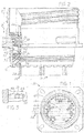
- Fig. 1 shows a connector 10 of the invention which includes a metal shell 12 having an axis 14, an insulator 16 within the shell, and a plurality of elongated contacts 20 that extend through holes in the insulator.
- the particular connector includes 128 contacts arranged in multiple rows 22 and lying within a shell having an outside diameter of about 41 mm (1.6 inches).
- the particular contacts are designed to carry low frequencies (e.g. DC to about one MHz), and the connector includes a filter for each contact that blocks high frequency noise, which is here generally defined as noise having a frequency above one MHz.
- Fig. 2 shows that the connector has a construction similar to that described in US 6,896,552 B (ITT MANUFACTURING ENTERPRISES, INC.) 24.05.2005 That is, the connector includes multiple elongated contacts 20 with opposite ends 26, 28 spaced in front F and rear R directions and that are accessible from opposite ends of the connector.
- a plurality of flexible circuit boards 31, 32, 33, and 34 extend across a cavity 36 formed in the shell 12, in planes that are normal to the connector axis.
- a rigidizing board 38 lies below portions of each circuit board.
- An inductor in the form of a ferrite bead 40 with front and rear ends 42, 44, is threaded around each contact.
- the boards carry capacitors 51, 52, 53 and 54 that are connected to the contact.
- the ferrite beads and capacitors provide filtering that blocks high frequency noise from passing along the contact.
- Many of the contacts of the connector are similarly filtered, with all of the contacts of the particular connector 10 being similarly filtered by providing a separate ferrite bead and set of capacitors for each contact.
- each board has a hole 60 through which the contact 20 extends.
- Each capacitor such as 51, has a pair of terminals, with one terminal 62 connected to a signal trace 64 on the circuit board that extends to, and preferably completely around the hole in the board.
- the signal trace is connected by a solder joint 66 to a location 71 on the contact.
- the other capacitor terminal 80 connects to a ground trace 82 that is electrically grounded.
- Fig. 4 shows that the ground trace extends to a periphery 84 of the board where the board is bent and soldered by a solder joint 86 to the metal shell.
- first and second capacitors 51, 52 were connected to the contact, at locations 71, 72, with one location 71 lying forward of the ferrite bead 40 and the other 72 lying rearward of the bead, to create a pi filter.
- applicant provides third and fourth capacitors 53, 54 that connect to contact connect locations 73, 74.
- One of the additional locations 73 where the third capacitor 53 connects to the contact lies forward of the ferrite bead 40 and is spaced a distance A from the first location 71.
- the other additional location 74, where the fourth capacitor 54 connects to the contact lies rearward of the ferrite bead and is spaced a distance B from the second location 72.
- Applicant calls the combination of a pi filter and at least two additional capacitors 53, 54, with an additional capacitor connected to a contact location lying beyond each end of the ferrite bead, an extended pi filter.
- Fig. 5 is a schematic diagram of the contact 20 and of the ferrite bead and capacitors.
- Fig 6 is a graph that qualitatively shows the advantage of applicant's extended pi filter over a prior pi filter. Below a frequency of about 100MHz, the filter characteristics are similar. However, considerably above 100 MHz, such as above 500 MHz, applicant's extended pi filter, whose performance is given by graph line 102, is better at attenuating very high frequency noise. Tests conducted by applicant show that at 1 GHz, the prior pi filter (with two 5000 picofarad capacitors), whose performance is given by graph line 104, produces an attenuation of -42dB, while applicant's extended pi filter (with four 2500 picofarad capacitors) produces an attenuation of -67dB. Also, applicant's extended pi filter has an attenuation that does not significantly decrease with increasing frequency near 1 GHz.
- Fig. 7 shows the effects of increasing the capacitance (to a plurality of times 5000 picofarads) of the two capacitors of a prior art pi filter, as compared to applicant's extended pi filter (with 4 capacitors of 2500 picofarads each and with an inductor having an inductance of 100 microhenries).
- Graph line 112 shows the performance of applicant's extended pi filter
- graph line 114 shows the performance of a prior pi filter with increased capacitance (two capacitors, each with a capacitance of a plurality of times 5000 picofarads). It can be seen that the effect of the high capacitance in a prior pi filter is to obtain greater attenuation of noise at lower frequencies such as below about 500 MHz, while reducing attenuation of noise with increasing frequency more rapidly than in applicant's extended pi filter.
- Fig. 4 shows that the contact pin portion 20A that extends through the ferrite bead 40 has a diameter D of 0,51 mm (0.020 inch).
- the first and second locations 71, 72 where the first and second capacitors connect to the contact arc spaced apart by a distance E of about 5,08 mm (0.200 inch).
- the distance A between the first contact connect location 71 and the third location 73, is 1,5 mm (0.060 inch).
- the distance B between the second and fourth contact connect locations is 1,5 mm (0.060 inch).
- Applicant tested the attenuation characteristics at both 1,0 mm (0.040 inch) and 1,5 mm (0.060 inch) separations and found that better attenuation was achieved at (1,5 mm (0.060 inch) separations. The separation should not exceed about 12,7 mm (0.5 inch).
- the connector of Fig. 4 can be assembled by positioning, in a fixture, a pair of insulator plates 130, 132 of the insulator 16, the four flexible circuit boards 31-34 with capacitors thereon, and the ferrite beads, all with their contact-receiving holes aligned.
- the contacts 20 are then inserted rearwardly though the holes, and the shell 12 is slid over the peripheries of the boards 31-34.
- the assembly is soldered to form the solder joints, and other parts such as elastomeric seals 140, 142 arc put in place.
- the center-to-center spacings A and B between capacitors that both lie beyond the same end of the ferrite bead should be a plurality of 0,025 mm thousandths inch (at least 0,1 mm) in any case, and preferably on the order of magnitude of 1,5 mm (0.060 inch). Applicant achieves an improvement in attenuation when the spacing A, B is at least equal to one half the diameter D of the contact portion that passes though the bead and capacitors, and especially when the spacing is at least equal to the contact diameter. Such spacing is preferably at least 1,5 mm (0.020 inch). As mentioned above, applicant has used spacings A, B of about 1,5 mm (1 to 2 mm) for best results while providing a filter arrangement that still fits into the connector of predetermined size.
Landscapes
- Details Of Connecting Devices For Male And Female Coupling (AREA)
- Filters And Equalizers (AREA)
Claims (9)
- Filter-Steckverbinder, der folgendes aufweist: eine Vielzahl von länglichen Kontakten (20), eine Vielzahl von Ferritkernen (40), die sich jeweils um einen der Kontakte erstrecken, wobei jeder Kern vordere und hintere Enden (42, 44) aufweist, und eine erste und eine zweite Vielzahl von Kondensatoren (51-54), die jeweils einen Signalanschluss (62) und einen geerdeten Erdanschluss (80) aufweisen, wobei der Signalanschluss von jedem der ersten Kondensatoren mit einem der Kontakte an einer ersten Stelle (71) verbunden ist, die vor dem vorderen Ende des entsprechenden Kerns liegt, und der Signalanschluss von jedem der zweiten Kondensatoren mit einem der Kontakte an einer zweiten Stelle (72) verbunden ist, die sich hinter dem hinteren Ende des entsprechenden Kerns befindet, dadurch gekennzeichnet, dass der Filter-Steckverbinder folgendes umfasst:eine dritte und eine vierte Vielzahl von Kondensatoren (53, 54), die jeweils geerdete Anschlüsse (80) aufweisen,wobei die dritten Kondensatoren jeweils einen Signalanschluss (62) aufweisen, der mit einem der Kontakte an einer dritten Stelle (73) verbunden ist, die vor dem vorderen Ende des entsprechenden Kerns liegt und die um einen Abstand A von der entsprechenden ersten Stelle (71) beabstandet ist;wobei die vierten Kondensatoren jeweils einen Signalanschluss (62) aufweisen, der mit einem der Kontakte an der vierten Stelle (74) verbunden ist, die hinter dem hinteren Ende des entsprechenden Kerns liegt, der um einen Abstand B von der entsprechenden zweiten Stelle (72) beabstandet ist.
- Steckverbinder nach Anspruch 1, wobei
die länglichen Kontakte (20) einen Durchmesser D aufweisen und
die Abstände A und B mindestens gleich einer Hälfte des Durchmessers D des länglichen Kontakts (20) sind. - Steckverbinder nach Anspruch 1, wobei:die ersten und dritten Stellen (71, 73) entlang eines Kontakts, wo sich entsprechende der ersten und dritten Kondensatoren mit dem entsprechenden Kontakt verbinden, um einen Abstand A von mindestens 0,1 mm beabstandet sind;die zweiten und vierten Stellen entlang eines Kontakts, wo sich entsprechende der zweiten und vierten Kondensatoren mit dem entsprechenden Kontakt verbinden, um einen Abstand B von mindestens 0,1 rnm beabstandet sind.
- Steckverbinder nach Anspruch 1, wobei:die Kondensatoren jeweils einen kapazitiven Widerstand in der Größenordnung von 2500 Picofarad aufweisen, wobei die ersten und dritten Stellen um einen Abstand A in der Größenordnung von 1,5 mm beabstandet sind, und die zweiten und vierten Stellen um einen Abstand B in der Größenordnung von 1,5 mm beabstandet sind.
- Steckverbinder nach Anspruch 1, wobei:der Steckverbinder ein Metallgehäuse (12) mit einer Achse (14) und mindestens vier Leiterplatten (31-34) aufweist, die sich senkrecht zu der Achse und beabstandet entlang der Achse erstrecken;wobei jede Leiterplatte eine Vielzahl von Löchern (60) aufweist, durch die sich die Kontakte erstrecken, und jede Leiterplatte eine Vielzahl von Signalspuren (64) aufweist, die sich um eines der Löcher und zum Kontakt daran angelötet erstrecken, wobei jeder Kondensator-Signalanschluss mit einer der Signalspuren verbunden ist;wobei die Leiterplatten mit ersten und dritten Platten (71, 73), die voneinander um einen Abstand A von mindestens 0,51 mm (0,02 inch) beabstandet sind, angeordnet sind, und wobei die ersten und dritten Platten beide vor den Kernen liegen, und die Leiterplatten mit zweiten und vierten Platten, die voneinander um einen Abstand B von mindestens 0,51 mm (0,02 inch) beabstandet sind, angeordnet sind, und wobei die zweiten und vierten Platten beide hinter den Kernen liegen.
- Steckverbinder nach Anspruch 1 oder 5, wobei:der Abstand zwischen der ersten und zweiten Platte größer ist als der Abstand zwischen der ersten und dritten Platte und größer ist als der Abstand zwischen der zweiten und vierten Platte.
- Steckverbinder nach Anspruch 1, wobei:der Abstand zwischen der ersten und dritten Platte, und der Abstand zwischen der zweiten und vierten Platte, jeweils in der Größenordnung von 1,5 mm liegt.
- Steckverbinder nach Anspruch 1 oder 7, wobei:und vierten Platten etwa 1,5 mm beträgt. die Kondensatoren des ersten, zweiten, dritten und vierten Satzes jeweils einen kapazitiven Widerstand in der Größenordnung von 2500 Picofarad aufweisen, der Abstand der ersten und dritten Platten etwa 1,5 mm, und der Abstand der zweiten
- Verfahren zum Blockieren von Hochfrequenzgeräuschen in der Größenordnung von einem MHz und höher in Strömen, die durch den länglichen Kontakt mit einem Durchmesser D fließen, dadurch gekennzeichnet, dass das Verfahren folgendes umfasst:Koppeln einer Spule mit einem vorderen und einem hinteren Ende mit dem Kontakt, der Signalanschlüsse von mindestens vier diskreten Kondensatoren mit vier verschiedenen Stellen auf dem Kontakt verbindet, und Verbinden von Erdanschlüssen der Kondensatoren mit der Erde;wobei der Schritt des Verbindens der Signalanschlüsse das Verbinden von ersten und dritten der Signalanschlüsse mit ersten und dritten der Stellen umfasst, die beide entlang der Länge des Leiters liegen und die vor dem vorderen Ende der Spule liegen und die um einen Abstand entsprechend mindestens der Hälfte des Durchmessers D des länglichen Kontakts beabstandet sind und zweite und vierte der Stellen verbinden, die beide hinter dem hinteren Ende der Spule liegen und die entlang der Länge des Leiters um einen Abstand entsprechend mindestens der Hälfte des Durchmessers D des länglichen Kontakts beabstandet sind.
Applications Claiming Priority (1)
| Application Number | Priority Date | Filing Date | Title |
|---|---|---|---|
| US10/932,951 US7014507B1 (en) | 2004-09-01 | 2004-09-01 | Filtered connector that blocks high frequency noise |
Publications (3)
| Publication Number | Publication Date |
|---|---|
| EP1633023A2 EP1633023A2 (de) | 2006-03-08 |
| EP1633023A3 EP1633023A3 (de) | 2012-05-16 |
| EP1633023B1 true EP1633023B1 (de) | 2016-10-26 |
Family
ID=35385544
Family Applications (1)
| Application Number | Title | Priority Date | Filing Date |
|---|---|---|---|
| EP05107243.7A Expired - Lifetime EP1633023B1 (de) | 2004-09-01 | 2005-08-05 | Gefilterter Steckverbinder der Hochfrequenzgeräusche blockt. |
Country Status (2)
| Country | Link |
|---|---|
| US (1) | US7014507B1 (de) |
| EP (1) | EP1633023B1 (de) |
Families Citing this family (7)
| Publication number | Priority date | Publication date | Assignee | Title |
|---|---|---|---|---|
| JP4381258B2 (ja) * | 2004-08-30 | 2009-12-09 | 株式会社オーディオテクニカ | マイクロホンコネクタ |
| IL187101A0 (en) * | 2006-11-20 | 2008-02-09 | Itt Mfg Enterprises Inc | Filter connector with high frequency shield |
| US7396256B2 (en) * | 2006-11-20 | 2008-07-08 | Itt Manufacturing Enterprises, Inc. | Filter connector with high frequency shield |
| CN104704682B (zh) * | 2012-08-22 | 2017-03-22 | 安费诺有限公司 | 高频电连接器 |
| JP6286765B2 (ja) * | 2012-09-28 | 2018-03-07 | 北川工業株式会社 | ノイズフィルタ付バスバー装置 |
| US8858262B2 (en) * | 2012-12-04 | 2014-10-14 | Genesis Technology Usa, Inc. | F-connector with integrated surge protection |
| DE112022005003T5 (de) * | 2021-10-20 | 2024-08-01 | Microchip Technology Incorporated | Vorrichtungen einschliesslich kondensator, der einen leistungspfad mit einem erdungspfad koppelt, und zugehörige komponenten und systeme |
Family Cites Families (20)
| Publication number | Priority date | Publication date | Assignee | Title |
|---|---|---|---|---|
| US3588758A (en) * | 1969-04-28 | 1971-06-28 | Itt | Electrical connector filter having dielectric and ferromagnetic tubes bonded together with conductive electrode layers and having nonintegral connecting spring |
| JPS6028447B2 (ja) * | 1978-06-22 | 1985-07-04 | 太陽誘電株式会社 | 複合lcフイルタ及びその製造方法 |
| US4458220A (en) * | 1981-07-17 | 1984-07-03 | Automation Industries, Inc. | Electrical connector and filter circuit |
| US4494092A (en) * | 1982-07-12 | 1985-01-15 | The Deutsch Company Electronic Components Division | Filter pin electrical connector |
| US4729743A (en) * | 1985-07-26 | 1988-03-08 | Amp Incorporated | Filtered electrical connector |
| US4729752A (en) * | 1985-07-26 | 1988-03-08 | Amp Incorporated | Transient suppression device |
| GB8703048D0 (en) * | 1987-02-11 | 1987-03-18 | Smiths Industries Plc | Filter arrangements |
| US4867706A (en) * | 1987-04-13 | 1989-09-19 | G & H Technology, Inc. | Filtered electrical connector |
| GB2205201B (en) * | 1987-05-21 | 1991-01-02 | Oxley Dev Co Ltd | Stress free integral filter array for multi-way connectors |
| US4853659A (en) * | 1988-03-17 | 1989-08-01 | Amp Incorporated | Planar pi-network filter assembly having capacitors formed on opposing surfaces of an inductive member |
| GB8915060D0 (en) * | 1989-06-30 | 1989-08-23 | Smiths Industries Plc | Electrical assemblies |
| IL97425A (en) * | 1991-03-04 | 1995-01-24 | Cohen Amir | author |
| US5580279A (en) * | 1994-10-31 | 1996-12-03 | Berg Technology, Inc. | Low cost filtered and shielded electronic connector and method of use |
| US5605477A (en) * | 1995-01-13 | 1997-02-25 | The Whitaker Corporation | Flexible etched circuit assembly |
| US5823827A (en) * | 1996-02-29 | 1998-10-20 | Berg Technology, Inc. | Low cost filtered and shielded electronic connector |
| US5838216A (en) * | 1996-09-06 | 1998-11-17 | Sunstrand Corporation | Common-mode EMI filter |
| US6218913B1 (en) * | 1998-02-18 | 2001-04-17 | Curtis Industries, A Division Of Powers Holatings, Inc. | Coaxial toroid EMI filter with discrete capacitors surrounding conductors |
| DE10064969B4 (de) * | 2000-01-20 | 2007-11-15 | Heidelberger Druckmaschinen Ag | Filtervorrichtung für mindestens eine von außen an ein Gehäuse anzuschließende elektrische Leitung |
| US6508672B1 (en) * | 2001-12-19 | 2003-01-21 | Itt Manufacturing Enterprises, Inc. | Joints for filter connector |
| US6896552B2 (en) * | 2003-05-06 | 2005-05-24 | Itt Manufacturing Enterprises, Inc. | Filtered connector |
-
2004
- 2004-09-01 US US10/932,951 patent/US7014507B1/en not_active Expired - Lifetime
-
2005
- 2005-08-05 EP EP05107243.7A patent/EP1633023B1/de not_active Expired - Lifetime
Also Published As
| Publication number | Publication date |
|---|---|
| EP1633023A3 (de) | 2012-05-16 |
| US7014507B1 (en) | 2006-03-21 |
| EP1633023A2 (de) | 2006-03-08 |
| US20060046571A1 (en) | 2006-03-02 |
Similar Documents
| Publication | Publication Date | Title |
|---|---|---|
| US5769667A (en) | Low cost filtered and shielded electronic connector | |
| US5736910A (en) | Modular jack connector with a flexible laminate capacitor mounted on a circuit board | |
| US4784618A (en) | Filter connector device | |
| US4401355A (en) | Filtered connector | |
| EP1052739B1 (de) | Abgeschirmte Verbindungsleiste | |
| US7540781B2 (en) | Electrical connector incorporating passive circuit elements | |
| US4144509A (en) | Filter connector | |
| US11721922B2 (en) | Multipole connector set | |
| US4781624A (en) | Filter arrangements and connectors | |
| US6794957B2 (en) | CATV filter assembly with improved electrical grounding | |
| US6737935B1 (en) | Diplex circuit forming bandstop filter | |
| IL97425A (en) | author | |
| CN112913085A (zh) | 印刷电路板连接器 | |
| JP4241732B2 (ja) | ノイズフィルタの実装構造 | |
| US5823827A (en) | Low cost filtered and shielded electronic connector | |
| EP1633023B1 (de) | Gefilterter Steckverbinder der Hochfrequenzgeräusche blockt. | |
| US9653847B2 (en) | High speed communication jack | |
| US6837747B1 (en) | Filtered connector | |
| US5379012A (en) | Dielectric filter device | |
| JP2002289309A (ja) | 電気コネクタ | |
| US20030090340A1 (en) | Signal filter | |
| EP0569917A1 (de) | Steckverbinder mit eingebautem Filter | |
| JP3275123B2 (ja) | 回路基板用フィルタコネクタ | |
| JP2006025144A (ja) | ノイズ除去方法およびノイズ除去回路 | |
| JPH05299140A (ja) | コネクタ |
Legal Events
| Date | Code | Title | Description |
|---|---|---|---|
| PUAI | Public reference made under article 153(3) epc to a published international application that has entered the european phase |
Free format text: ORIGINAL CODE: 0009012 |
|
| AK | Designated contracting states |
Kind code of ref document: A2 Designated state(s): AT BE BG CH CY CZ DE DK EE ES FI FR GB GR HU IE IS IT LI LT LU LV MC NL PL PT RO SE SI SK TR |
|
| AX | Request for extension of the european patent |
Extension state: AL BA HR MK YU |
|
| PUAL | Search report despatched |
Free format text: ORIGINAL CODE: 0009013 |
|
| AK | Designated contracting states |
Kind code of ref document: A3 Designated state(s): AT BE BG CH CY CZ DE DK EE ES FI FR GB GR HU IE IS IT LI LT LU LV MC NL PL PT RO SE SI SK TR |
|
| AX | Request for extension of the european patent |
Extension state: AL BA HR MK YU |
|
| RIC1 | Information provided on ipc code assigned before grant |
Ipc: H01R 13/719 20110101AFI20120410BHEP |
|
| RAP1 | Party data changed (applicant data changed or rights of an application transferred) |
Owner name: ITT MANUFACTURING ENTERPRISES LLC |
|
| 17P | Request for examination filed |
Effective date: 20121116 |
|
| AKX | Designation fees paid |
Designated state(s): DE FR GB IT SE |
|
| GRAP | Despatch of communication of intention to grant a patent |
Free format text: ORIGINAL CODE: EPIDOSNIGR1 |
|
| INTG | Intention to grant announced |
Effective date: 20160520 |
|
| GRAS | Grant fee paid |
Free format text: ORIGINAL CODE: EPIDOSNIGR3 |
|
| GRAA | (expected) grant |
Free format text: ORIGINAL CODE: 0009210 |
|
| AK | Designated contracting states |
Kind code of ref document: B1 Designated state(s): DE FR GB IT SE |
|
| REG | Reference to a national code |
Ref country code: GB Ref legal event code: FG4D |
|
| REG | Reference to a national code |
Ref country code: DE Ref legal event code: R096 Ref document number: 602005050511 Country of ref document: DE |
|
| PG25 | Lapsed in a contracting state [announced via postgrant information from national office to epo] |
Ref country code: SE Free format text: LAPSE BECAUSE OF FAILURE TO SUBMIT A TRANSLATION OF THE DESCRIPTION OR TO PAY THE FEE WITHIN THE PRESCRIBED TIME-LIMIT Effective date: 20161026 |
|
| REG | Reference to a national code |
Ref country code: DE Ref legal event code: R097 Ref document number: 602005050511 Country of ref document: DE |
|
| PG25 | Lapsed in a contracting state [announced via postgrant information from national office to epo] |
Ref country code: IT Free format text: LAPSE BECAUSE OF FAILURE TO SUBMIT A TRANSLATION OF THE DESCRIPTION OR TO PAY THE FEE WITHIN THE PRESCRIBED TIME-LIMIT Effective date: 20161026 |
|
| PLBE | No opposition filed within time limit |
Free format text: ORIGINAL CODE: 0009261 |
|
| STAA | Information on the status of an ep patent application or granted ep patent |
Free format text: STATUS: NO OPPOSITION FILED WITHIN TIME LIMIT |
|
| 26N | No opposition filed |
Effective date: 20170727 |
|
| PGFP | Annual fee paid to national office [announced via postgrant information from national office to epo] |
Ref country code: DE Payment date: 20170829 Year of fee payment: 13 |
|
| GBPC | Gb: european patent ceased through non-payment of renewal fee |
Effective date: 20170805 |
|
| REG | Reference to a national code |
Ref country code: FR Ref legal event code: ST Effective date: 20180430 |
|
| PG25 | Lapsed in a contracting state [announced via postgrant information from national office to epo] |
Ref country code: GB Free format text: LAPSE BECAUSE OF NON-PAYMENT OF DUE FEES Effective date: 20170805 |
|
| PG25 | Lapsed in a contracting state [announced via postgrant information from national office to epo] |
Ref country code: FR Free format text: LAPSE BECAUSE OF NON-PAYMENT OF DUE FEES Effective date: 20170831 |
|
| REG | Reference to a national code |
Ref country code: DE Ref legal event code: R119 Ref document number: 602005050511 Country of ref document: DE |
|
| PG25 | Lapsed in a contracting state [announced via postgrant information from national office to epo] |
Ref country code: DE Free format text: LAPSE BECAUSE OF NON-PAYMENT OF DUE FEES Effective date: 20190301 |