EP1632973A2 - Galette de microcanaux ayant des segments servant de patte de montage - Google Patents
Galette de microcanaux ayant des segments servant de patte de montage Download PDFInfo
- Publication number
- EP1632973A2 EP1632973A2 EP05255398A EP05255398A EP1632973A2 EP 1632973 A2 EP1632973 A2 EP 1632973A2 EP 05255398 A EP05255398 A EP 05255398A EP 05255398 A EP05255398 A EP 05255398A EP 1632973 A2 EP1632973 A2 EP 1632973A2
- Authority
- EP
- European Patent Office
- Prior art keywords
- microchannel plate
- array
- fibers
- set forth
- active area
- Prior art date
- Legal status (The legal status is an assumption and is not a legal conclusion. Google has not performed a legal analysis and makes no representation as to the accuracy of the status listed.)
- Granted
Links
- 239000011521 glass Substances 0.000 claims abstract description 30
- 239000007787 solid Substances 0.000 claims abstract description 27
- 238000004519 manufacturing process Methods 0.000 claims abstract description 14
- 230000036571 hydration Effects 0.000 claims abstract description 8
- 238000006703 hydration reaction Methods 0.000 claims abstract description 8
- 238000005336 cracking Methods 0.000 claims abstract description 6
- 230000008961 swelling Effects 0.000 claims abstract description 3
- 230000002093 peripheral effect Effects 0.000 claims abstract 4
- 239000000835 fiber Substances 0.000 claims description 37
- 238000000034 method Methods 0.000 claims description 10
- 238000003491 array Methods 0.000 claims description 5
- 238000007872 degassing Methods 0.000 claims 1
- 239000007789 gas Substances 0.000 description 5
- 239000011148 porous material Substances 0.000 description 5
- 235000012431 wafers Nutrition 0.000 description 5
- UFHFLCQGNIYNRP-UHFFFAOYSA-N Hydrogen Chemical compound [H][H] UFHFLCQGNIYNRP-UHFFFAOYSA-N 0.000 description 3
- VYPSYNLAJGMNEJ-UHFFFAOYSA-N Silicium dioxide Chemical compound O=[Si]=O VYPSYNLAJGMNEJ-UHFFFAOYSA-N 0.000 description 3
- 239000001257 hydrogen Substances 0.000 description 3
- 229910052739 hydrogen Inorganic materials 0.000 description 3
- 239000002184 metal Substances 0.000 description 3
- 239000002245 particle Substances 0.000 description 3
- 238000011282 treatment Methods 0.000 description 3
- XLYOFNOQVPJJNP-UHFFFAOYSA-N water Chemical compound O XLYOFNOQVPJJNP-UHFFFAOYSA-N 0.000 description 3
- 239000003513 alkali Substances 0.000 description 2
- 238000010586 diagram Methods 0.000 description 2
- 230000000694 effects Effects 0.000 description 2
- 230000005670 electromagnetic radiation Effects 0.000 description 2
- 238000012986 modification Methods 0.000 description 2
- 230000004048 modification Effects 0.000 description 2
- 230000004297 night vision Effects 0.000 description 2
- 238000005498 polishing Methods 0.000 description 2
- 239000000126 substance Substances 0.000 description 2
- 235000002595 Solanum tuberosum Nutrition 0.000 description 1
- 244000061456 Solanum tuberosum Species 0.000 description 1
- 238000010521 absorption reaction Methods 0.000 description 1
- 238000004458 analytical method Methods 0.000 description 1
- 238000013459 approach Methods 0.000 description 1
- 239000008280 blood Substances 0.000 description 1
- 210000004369 blood Anatomy 0.000 description 1
- 230000001351 cycling effect Effects 0.000 description 1
- 238000009792 diffusion process Methods 0.000 description 1
- 238000007876 drug discovery Methods 0.000 description 1
- 230000005684 electric field Effects 0.000 description 1
- 238000013100 final test Methods 0.000 description 1
- 239000003365 glass fiber Substances 0.000 description 1
- 238000007689 inspection Methods 0.000 description 1
- 150000002500 ions Chemical class 0.000 description 1
- 239000005355 lead glass Substances 0.000 description 1
- 239000000463 material Substances 0.000 description 1
- 239000000203 mixture Substances 0.000 description 1
- 230000003287 optical effect Effects 0.000 description 1
- 238000012545 processing Methods 0.000 description 1
- 238000009877 rendering Methods 0.000 description 1
- 238000011160 research Methods 0.000 description 1
- 239000004065 semiconductor Substances 0.000 description 1
- 230000035945 sensitivity Effects 0.000 description 1
- 230000035939 shock Effects 0.000 description 1
- 239000000741 silica gel Substances 0.000 description 1
- 229910002027 silica gel Inorganic materials 0.000 description 1
- 239000005368 silicate glass Substances 0.000 description 1
- 239000000377 silicon dioxide Substances 0.000 description 1
- 230000002269 spontaneous effect Effects 0.000 description 1
- 238000004381 surface treatment Methods 0.000 description 1
- 238000012360 testing method Methods 0.000 description 1
- 238000002207 thermal evaporation Methods 0.000 description 1
- 238000009489 vacuum treatment Methods 0.000 description 1
Images


Classifications
-
- H—ELECTRICITY
- H01—ELECTRIC ELEMENTS
- H01J—ELECTRIC DISCHARGE TUBES OR DISCHARGE LAMPS
- H01J43/00—Secondary-emission tubes; Electron-multiplier tubes
- H01J43/04—Electron multipliers
- H01J43/06—Electrode arrangements
- H01J43/18—Electrode arrangements using essentially more than one dynode
- H01J43/24—Dynodes having potential gradient along their surfaces
- H01J43/246—Microchannel plates [MCP]
-
- H—ELECTRICITY
- H01—ELECTRIC ELEMENTS
- H01J—ELECTRIC DISCHARGE TUBES OR DISCHARGE LAMPS
- H01J2237/00—Discharge tubes exposing object to beam, e.g. for analysis treatment, etching, imaging
- H01J2237/244—Detection characterized by the detecting means
- H01J2237/24435—Microchannel plates
Definitions
- Microchannel plates are high gain, low noise, solid-state electron multipliers consisting of millions of tiny, alkali doped lead glass channels all fused together into a solid array.
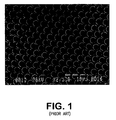
- Figure 1 is a photomicrograph illustrating the microchannel structure. These devices are sensitive to a wide range of charged particles and electro-magnetic radiation and are fabricated in sizes ranging from 3 to 150 millimeters in diameter.
- charged particles ions, electrons
- electromagnetic radiation UV Photon, Soft X-Rays
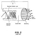
- the secondary electrons accelerate through the channel toward the output side of the channel, driven by the ever increasing positive electric potential created by current flowing within the resistive layer of the channel structure.
- Subsequent collisions of the secondary electrons with the channel wall create further secondary electrons in a cascade until the charge exits the channel and is recorded on a readout device. Varying the voltage applied across the array will vary the gain by influencing the number of collisions and the number of secondary electrons generated upon each successive collision with the channel wall.
- Typical microchannel plates can produce approximately 10,000 electrons for every single charged particle impinging on the input surface. Microchannel plates can be stacked together in order to obtain improved performance. When two MCP's are stacked, the resultant device has a typical gain of about 10,000,000 (10 7 ). Stacking three MCP's together provides a gain of up to about 100,000,000 (10 8 ).
- Microchannel plates were originally developed for image intensifiers used in night vision scopes.
- Today, microchannel plates are used in a wide variety of commercial and scientific applications ranging from space exploration (the Hubble Space Telescope contains several instruments employing microchannel plates) to semiconductor processing, to drug discovery, cancer research, and anti-terrorist activities.
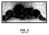
- Microchannel plates are no longer limited to the small formats developed for night vision and are produced in sizes ranging from 3 to 150 mm in diameter or other major dimension. Shown in Figure 3 are some known product forms of microchannel plates.
- microchannel plate detectors in medical instruments enable blood analyzers to function. Mass spectrometers with parts per billion analysis capabilities only function when equipped with MCP detectors. Many pharmaceutical and medical breakthroughs of the last 10 years would not have occurred if it were not for microchannel plates. Unlike MCP's used in image intensifier tubes, MCP's for analytical instruments frequently need to be cycled from high vacuum to atmospheric pressure.
- microchannel plates In order to operate a microchannel plate it must be mounted in a conductive fixture which makes electrical contact to the electrodes which are formed on each side of the plate.
- the electrodes are used to apply the high voltage needed to create an electric field within the channels that sustains the secondary electron emission.
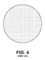
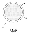
- microchannel plates When microchannel plates were first invented, they had very large pores (i.e., about 50 microns in diameter) and thick channel walls (i.e., about 12 microns thick). They had active channels extending all the way out to the very edge of the MCP as shown in Figure 4. Making electrical connection to such a structure was accommodated by simply sandwiching the MCP disk between two metal washers.
- That structure provided very good support for the MCP and was successfully optimized for high shock and vibration environments.
- the relatively wide channel walls easily supported the structure with enough surface area to make good electrical contact without causing mechanical damage to the array.
- Microchannel plates are manufactured from alkali doped lead silicate glass.
- the active surfaces of a microchannel plate, within the channels are essentially a fired silica gel. This surface is known to be very hygroscopic, that is, it absorbs water vapor readily from the ambient environment.
- the composition of the channel walls of a microchannel plate, regardless of glass type or manufacturer, are chemically almost identical to that material used in silica desiccating packs used to absorb water and keep clothing, electronics, and other products dry.
- the porous nature of the microchannel plate structure means that the active area can have several hundred times the surface area of the nonporous solid glass rim.
- microchannel plates When microchannel plates are manufactured they are machined parallel and flat to within 20 microns.
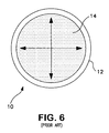
- the active area 14 swells as illustrated in Figure 6 and begins to expand in the directions illustrated by the arrows. As the active area 14 expands it begins to push against the solid glass border 12 which expands at a much slower rate, based on the difference in the surface area.
- Continued expansion of the active area 14 causes the microchannel plate 10 to become distorted, i.e., concave on one side and convex on the other. Further expansion of the active area 14 will eventually cause the solid glass border 12 to fail in tension by cracking.
- the classic hydration failure is characterized by a crack originating at the edge of the MCP 10 and extending toward the center of the MCP.
- the crack is wider at the perimeter of the solid glass rim 12 than in the center of the active area 14. This behavior can be modeled using hoop stress equations.
- microchannel plate structure which will tolerate an expansion of the active area and provide a mounting structure which will provide good electrical contact, without damaging the active channels.
- the desired structure should not trap gas within unused channels.
- a microchannel plate which has an active area and at least one solid glass pad.
- the active area has a plurality of microchannels formed therein.
- the solid glass pad or pads are formed within the active area for mounting the microchannel plate in an operative device.
- a method of making a microchannel plate includes the step of assembling an array of elongated multi-fibers in a vessel. At least one segment array of elongated cane fibers is inserted at a location within the array of elongated multi-fibers in the vessel to form a fiber assembly. The fibers in the fiber assembly are then fused together to form a billet. In a preferred embodiment of the method according to this invention, two or more segment arrays of the elongated cane fibers are inserted in the multi-fiber array at spaced locations around the periphery of the multi-fiber array.
- FIG. 7 illustrates an experimental embodiment of a microchannel plate 710 according to the present invention.
- first and second solid glass pads 712a and 712b are formed on either side of the active channel area 714. Hydration testing confirmed that the configuration shown in Figure 7 did not spontaneously crack from exposure to moisture.
- FIG 8 illustrates a preferred arrangement for a microchannel plate according to this invention.
- strategically placed mounting pads 812a, 812b, 812c, and 812d composed of solid glass, are disposed about the periphery of the MCP 810.
- An area 814 of active channels is disposed between and around the mounting pads 812a, 812b, 812c, and 812d.
- microchannel plate structure shown in Figures 7 and 8 solves the problems caused by expansion of the active areas from the absorption of water vapor.
- the relatively large spaces between the solid mounting pads allow the active area to swell and expand substantially unimpeded.
- Microchannel plates according to the present invention were stored in ambient room air for over 12 months and did not show any signs of warping or cracking.
- FIG. 9 illustrates the major manufacturing steps in the microchannel plate fabrication process according to this invention.
- Microchannel plates according to the present invention are fabricated through a series of fiber draws and redraws as in steps 910 and 920. The fibers are assembled and then fused together to form a billet as in step 930.
- the fabricator follows a fabrication drawing to assemble a plurality of multi-fibers in an array, which will become the active channels. Segment arrays of cane fibers, which will become the mounting pads, are inserted into the multi-fiber array in specific areas.
- Figure 10 illustrates an example of an assembly of the multi- and cane fibers for fabricating a microchannel plate billet according to this invention.
- the cane fibers 1012 and the multi-fibers 1014 are placed in a bottle 1016.
- the cane fibers are arranged within the multi-fibers in quantities and at locations to provide solid glass mounting pads of desired size and at desired locations about the periphery of the multi-fiber array.
- the fibers are fused together.
- the fused billet is then wafered (sliced), ground, and then polished in step 940.
- the grinding and polishing operations produce,a very smooth surface and subsurface finish on the input and output sides of the wafers that become the microchannel plates.
- the MCP wafers are subjected to a combination of mechanical and chemical treatments to their surfaces in step 950.
- the treatments not only produce an optical finish on the MCP, but also cause the solid glass areas (the mounting pads) to become slightly elevated (about 2-10 microns) relative to the active area.
- the elevated mounting pad areas prevent the trapping of gasses within the channels that lie underneath the mounting hardware when the MCP is mounted in an operative device. Eliminating trapped gas under the mounting hardware permits faster pump down to the desired vacuum, eliminates the generation of plasma, and thereby reduces noise in the array during operation.
- the MCP wafers are subjected to a hydrogen reduction treatment in step 960.
- the microchannel plate wafer undergoes significant shrinkage during the cool down process following the hydrogen reduction step.
- the difference in the shrinkage between the continuous glass rim and the active area frequently caused the MCP to warp in a "potato chip" fashion.
- the use of the non-continuous (segmented) solid glass mounting pads in accordance with this invention also effectively eliminates the warping effect and thereby increases MCP production yields.
- the surfaces of the MCP wafers are metallized by evaporative deposition, step 970, to form conductive electrodes on the surfaces.
- the finished microchannel plates are then given a final test and inspection in step 980.
Applications Claiming Priority (1)
| Application Number | Priority Date | Filing Date | Title |
|---|---|---|---|
| US60706004P | 2004-09-03 | 2004-09-03 |
Publications (3)
| Publication Number | Publication Date |
|---|---|
| EP1632973A2 true EP1632973A2 (fr) | 2006-03-08 |
| EP1632973A3 EP1632973A3 (fr) | 2010-05-26 |
| EP1632973B1 EP1632973B1 (fr) | 2016-08-31 |
Family
ID=35448035
Family Applications (1)
| Application Number | Title | Priority Date | Filing Date |
|---|---|---|---|
| EP05255398.9A Active EP1632973B1 (fr) | 2004-09-03 | 2005-09-02 | Galette de microcanaux ayant des segments servant de patte de montage |
Country Status (2)
| Country | Link |
|---|---|
| US (1) | US7555185B2 (fr) |
| EP (1) | EP1632973B1 (fr) |
Cited By (1)
| Publication number | Priority date | Publication date | Assignee | Title |
|---|---|---|---|---|
| WO2022229917A1 (fr) * | 2021-04-29 | 2022-11-03 | Dh Technologies Development Pte. Ltd. | Cartouche de micro-canal pour spectromètre de masse |
Families Citing this family (8)
| Publication number | Priority date | Publication date | Assignee | Title |
|---|---|---|---|---|
| US7555185B2 (en) * | 2004-09-03 | 2009-06-30 | Burle Technologies, Inc. | Microchannel plate with segmented mounting pads |
| JP5388735B2 (ja) * | 2009-07-21 | 2014-01-15 | 浜松ホトニクス株式会社 | マイクロチャンネルプレート |
| US8101913B2 (en) * | 2009-09-11 | 2012-01-24 | Ut-Battelle, Llc | Method of making large area conformable shape structures for detector/sensor applications using glass drawing technique and postprocessing |
| US8410442B2 (en) | 2010-10-05 | 2013-04-02 | Nathaniel S. Hankel | Detector tube stack with integrated electron scrub system and method of manufacturing the same |
| JP6434361B2 (ja) * | 2015-04-27 | 2018-12-05 | 浜松ホトニクス株式会社 | マイクロチャンネルプレート |
| GB201618023D0 (en) | 2016-10-25 | 2016-12-07 | Micromass Uk Limited | Ion detection system |
| WO2023057933A1 (fr) * | 2021-10-06 | 2023-04-13 | Dh Technologies Development Pte. Ltd. | Ensemble de montage de plaque à microcanaux pour détecteur d'ions en spectrométrie de masse |
| CN114988692B (zh) * | 2022-05-17 | 2024-01-23 | 北方夜视科技(南京)研究院有限公司 | 改善微通道板制备过程中复丝顶角错位的方法 |
Family Cites Families (9)
| Publication number | Priority date | Publication date | Assignee | Title |
|---|---|---|---|---|
| FR2086673A5 (fr) * | 1970-04-06 | 1971-12-31 | Labo Electronique Physique | |
| US4005323A (en) * | 1971-11-15 | 1977-01-25 | American Optical Corporation | Microchannel plates in glass mountings |
| US4737013A (en) * | 1986-11-03 | 1988-04-12 | Litton Systems, Inc. | Microchannel plate having an etch limiting barrier |
| US4849000A (en) * | 1986-11-26 | 1989-07-18 | The United States Of America As Represented By The Secretary Of The Army | Method of making fiber optic plates for wide angle and graded acuity intensifier tubes |
| US4886537A (en) * | 1988-04-21 | 1989-12-12 | The United States Of America As Represented By The Secretary Of The Army | Method of making wide angle and graded acuity intensifier tubes |
| US6311001B1 (en) * | 1998-10-16 | 2001-10-30 | Ltt Manufacturing Enterprises | Microchannel plate having microchannels with funneled openings and method for manufacturing same |
| US6876802B2 (en) * | 2002-11-26 | 2005-04-05 | Itt Manufacturing Enterprises, Inc. | Microchannel plate having microchannels with deep funneled and/or step funneled openings and method of manufacturing same |
| US7555185B2 (en) * | 2004-09-03 | 2009-06-30 | Burle Technologies, Inc. | Microchannel plate with segmented mounting pads |
| US7251400B1 (en) * | 2005-06-13 | 2007-07-31 | Itt Manufacturing Enterprises, Inc. | Absorptive clad fiber optic faceplate tube |
-
2005
- 2005-09-01 US US11/217,873 patent/US7555185B2/en active Active
- 2005-09-02 EP EP05255398.9A patent/EP1632973B1/fr active Active
Non-Patent Citations (1)
| Title |
|---|
| None |
Cited By (1)
| Publication number | Priority date | Publication date | Assignee | Title |
|---|---|---|---|---|
| WO2022229917A1 (fr) * | 2021-04-29 | 2022-11-03 | Dh Technologies Development Pte. Ltd. | Cartouche de micro-canal pour spectromètre de masse |
Also Published As
| Publication number | Publication date |
|---|---|
| US7555185B2 (en) | 2009-06-30 |
| EP1632973B1 (fr) | 2016-08-31 |
| US20070236118A1 (en) | 2007-10-11 |
| EP1632973A3 (fr) | 2010-05-26 |
Similar Documents
| Publication | Publication Date | Title |
|---|---|---|
| EP1632973B1 (fr) | Galette de microcanaux ayant des segments servant de patte de montage | |
| US6127777A (en) | Field emission display with non-evaporable getter material | |
| EP2811510B1 (fr) | Suppression électrostatique de rétroaction d'ions dans un photomultiplicateur à galette de microcanaux | |
| JP2010103110A (ja) | 画像センサーを位置合わせする装置及び方法 | |
| US8022606B2 (en) | Electron multipler and electron detector | |
| Grzebyk et al. | Glow-discharge ion-sorption micropump for vacuum MEMS | |
| US9214326B2 (en) | Atmospheric pressure chemical ionization ion source | |
| US4978885A (en) | Electron multipliers with reduced ion feedback | |
| US3783299A (en) | X-ray image intensifier input phosphor screen and method of manufacture thereof | |
| JP2000048743A (ja) | 平面形撮像装置及びその製造方法 | |
| KR20170031179A (ko) | 양극, 및 이를 이용한 x선 발생관, x선 발생 장치, 및 방사선촬영 시스템 | |
| WO2013172417A1 (fr) | Galette de microcanaux | |
| US4355229A (en) | Intensified charge coupled image sensor having universal header assembly | |
| US20040135493A1 (en) | Field emission display and method of manufacturing the same | |
| US3852131A (en) | Method of manufacturing x-ray image intensifier input phosphor screen | |
| US4406973A (en) | Black glass shield and method for absorbing stray light for image intensifiers | |
| US4604519A (en) | Intensified charge coupled image sensor having an improved CCD support | |
| US3262002A (en) | Convertible x-ray detector | |
| US9911584B2 (en) | Batch production of microchannel plate photo-multipliers | |
| US7982172B2 (en) | Micro channel plate assembly | |
| Laprade | Advancement in microchannel-plate technology | |
| US20040245925A1 (en) | Electron tube and method of manufacturing the electron tube | |
| JPH0347032B2 (fr) | ||
| Timothy | Performance characteristics of the imaging MAMA detector systems for SOHO, STIS, and FUSE/Lyman | |
| Malina et al. | Comparative lifetesting results for microchannel plates in windowless EUV photon detectors |
Legal Events
| Date | Code | Title | Description |
|---|---|---|---|
| PUAI | Public reference made under article 153(3) epc to a published international application that has entered the european phase |
Free format text: ORIGINAL CODE: 0009012 |
|
| AK | Designated contracting states |
Kind code of ref document: A2 Designated state(s): AT BE BG CH CY CZ DE DK EE ES FI FR GB GR HU IE IS IT LI LT LU LV MC NL PL PT RO SE SI SK TR |
|
| AX | Request for extension of the european patent |
Extension state: AL BA HR MK YU |
|
| PUAL | Search report despatched |
Free format text: ORIGINAL CODE: 0009013 |
|
| AK | Designated contracting states |
Kind code of ref document: A3 Designated state(s): AT BE BG CH CY CZ DE DK EE ES FI FR GB GR HU IE IS IT LI LT LU LV MC NL PL PT RO SE SI SK TR |
|
| AX | Request for extension of the european patent |
Extension state: AL BA HR MK YU |
|
| 17P | Request for examination filed |
Effective date: 20101123 |
|
| AKX | Designation fees paid |
Designated state(s): DE FR GB NL |
|
| 17Q | First examination report despatched |
Effective date: 20120124 |
|
| GRAP | Despatch of communication of intention to grant a patent |
Free format text: ORIGINAL CODE: EPIDOSNIGR1 |
|
| INTG | Intention to grant announced |
Effective date: 20160330 |
|
| GRAS | Grant fee paid |
Free format text: ORIGINAL CODE: EPIDOSNIGR3 |
|
| GRAA | (expected) grant |
Free format text: ORIGINAL CODE: 0009210 |
|
| AK | Designated contracting states |
Kind code of ref document: B1 Designated state(s): DE FR GB NL |
|
| REG | Reference to a national code |
Ref country code: GB Ref legal event code: FG4D |
|
| REG | Reference to a national code |
Ref country code: FR Ref legal event code: PLFP Year of fee payment: 12 |
|
| REG | Reference to a national code |
Ref country code: DE Ref legal event code: R096 Ref document number: 602005050109 Country of ref document: DE |
|
| REG | Reference to a national code |
Ref country code: NL Ref legal event code: FP |
|
| REG | Reference to a national code |
Ref country code: DE Ref legal event code: R097 Ref document number: 602005050109 Country of ref document: DE |
|
| PLBE | No opposition filed within time limit |
Free format text: ORIGINAL CODE: 0009261 |
|
| STAA | Information on the status of an ep patent application or granted ep patent |
Free format text: STATUS: NO OPPOSITION FILED WITHIN TIME LIMIT |
|
| 26N | No opposition filed |
Effective date: 20170601 |
|
| REG | Reference to a national code |
Ref country code: FR Ref legal event code: PLFP Year of fee payment: 13 |
|
| REG | Reference to a national code |
Ref country code: FR Ref legal event code: PLFP Year of fee payment: 14 |
|
| P01 | Opt-out of the competence of the unified patent court (upc) registered |
Effective date: 20230521 |
|
| PGFP | Annual fee paid to national office [announced via postgrant information from national office to epo] |
Ref country code: NL Payment date: 20230926 Year of fee payment: 19 Ref country code: GB Payment date: 20230927 Year of fee payment: 19 |
|
| PGFP | Annual fee paid to national office [announced via postgrant information from national office to epo] |
Ref country code: FR Payment date: 20230925 Year of fee payment: 19 Ref country code: DE Payment date: 20230927 Year of fee payment: 19 |