EP1632865B1 - Interface de bus de données pour un appareil de commande et un appareil de commande avec une interface de bus de données - Google Patents
Interface de bus de données pour un appareil de commande et un appareil de commande avec une interface de bus de données Download PDFInfo
- Publication number
- EP1632865B1 EP1632865B1 EP05106497A EP05106497A EP1632865B1 EP 1632865 B1 EP1632865 B1 EP 1632865B1 EP 05106497 A EP05106497 A EP 05106497A EP 05106497 A EP05106497 A EP 05106497A EP 1632865 B1 EP1632865 B1 EP 1632865B1
- Authority
- EP
- European Patent Office
- Prior art keywords
- data bus
- transmission
- controller
- bus interface
- transceiver
- Prior art date
- Legal status (The legal status is an assumption and is not a legal conclusion. Google has not performed a legal analysis and makes no representation as to the accuracy of the status listed.)
- Not-in-force
Links
- 230000005540 biological transmission Effects 0.000 claims description 30
- 238000004891 communication Methods 0.000 claims description 16
- 230000008901 benefit Effects 0.000 description 8
- 238000012544 monitoring process Methods 0.000 description 5
- 238000012546 transfer Methods 0.000 description 4
- 238000011161 development Methods 0.000 description 3
- 230000002457 bidirectional effect Effects 0.000 description 2
- 230000006855 networking Effects 0.000 description 2
- 238000002485 combustion reaction Methods 0.000 description 1
- 238000004590 computer program Methods 0.000 description 1
- 230000003750 conditioning effect Effects 0.000 description 1
- 238000010276 construction Methods 0.000 description 1
- 230000008878 coupling Effects 0.000 description 1
- 238000010168 coupling process Methods 0.000 description 1
- 238000005859 coupling reaction Methods 0.000 description 1
- 238000013461 design Methods 0.000 description 1
- 230000000694 effects Effects 0.000 description 1
- 238000009472 formulation Methods 0.000 description 1
- 238000004519 manufacturing process Methods 0.000 description 1
- 239000000203 mixture Substances 0.000 description 1
- 230000008520 organization Effects 0.000 description 1
- 230000003071 parasitic effect Effects 0.000 description 1
- 230000001105 regulatory effect Effects 0.000 description 1
- 238000012360 testing method Methods 0.000 description 1
- 230000001960 triggered effect Effects 0.000 description 1
Images

Classifications
-
- G—PHYSICS
- G06—COMPUTING; CALCULATING OR COUNTING
- G06F—ELECTRIC DIGITAL DATA PROCESSING
- G06F13/00—Interconnection of, or transfer of information or other signals between, memories, input/output devices or central processing units
- G06F13/38—Information transfer, e.g. on bus
- G06F13/382—Information transfer, e.g. on bus using universal interface adapter
- G06F13/385—Information transfer, e.g. on bus using universal interface adapter for adaptation of a particular data processing system to different peripheral devices
Definitions
- the present invention relates to a data bus interface for a control unit, in particular for a motor vehicle control unit.
- the invention also relates to a control device, in particular a motor vehicle control device, having a data bus interface for accessing a data bus for communication with at least one other control device via the data bus.
- the interface here is an interface between one or more microprocessors on the one hand and a data bus on the other hand.
- the interface prepares signals from a microprocessor to be transferred via a data bus to another microprocessor according to a selected transmission protocol (eg CAN (Controller Area Network), TTCAN (Time Triggered CAN), MOST (Media Oriented Systems Transport), FlexRay, etc.) before they are injected onto the data bus.
- a transmission protocol eg CAN (Controller Area Network), TTCAN (Time Triggered CAN), MOST (Media Oriented Systems Transport), FlexRay, etc.
- the interface may be part of a control unit, in particular part of a motor vehicle control unit. Then on the Control programs are executed to fulfill a proper control and / or regulation function and they can serve to control and coordinate the communication over the data buses.
- the microcontrollers of the interface merely serve to control and coordinate the communication via the data buses and receive the data to be transmitted from other microcontrollers and only forward the received data.
- at least one control unit can be connected to a data bus. The control units connected to the same data bus can then exchange information with one another via the data bus.
- WO 98/44399 discloses a data bus interface with two microprocessors communicating with each other via a data bus.
- the present invention is based on the object to design a data bus interface of the type mentioned in such a way and further, that it can be used very flexible and is inexpensive to manufacture.
- microprocessors and the transceivers of the data bus interfaces according to the invention are integrated on a common printed circuit board.
- the microprocessors in the form of microcontrollers each have two data bus controllers to increase the communication capability of the interface.
- One of the data bus controllers is used for external communication of the microcontroller with corresponding microcontrollers in other data bus interfaces and the other data bus controller is used for internal communication between the microcontrollers.
- At least one external data bus is provided.
- the at least one data bus is arranged outside the data bus interface.
- Each of the microcontrollers is connected to the at least one external data bus via a common or in each case a separate transceiver unit (transceiver).
- the microcontroller of the data bus interfaces according to the invention are connected to other data bus interfaces or to their microcontrollers and can exchange information with them via the at least one external data bus.
- the microcontrollers are each connected to the transceivers via one of their data bus controllers (the so-called first data bus controller).
- the two transceivers are connected to one and the same external data bus. More specifically, the first data bus controllers of both transceivers are connected to the same data bus. Due to the fact that each data bus controller can manage only a certain number of message objects (so-called message objects), this embodiment of the invention has the advantage that the data bus interface according to the invention for a particular data bus significantly more, in the present case with two Microcontrollers namely exactly twice as many, can manage message objects.
- message objects message objects
- the two transceivers are connected to different external data buses.
- the different data buses can operate at the same or different transmission rates.
- signals are transmitted via the two data buses according to different or the same transmission speeds.
- the data bus interface according to the invention could work, for example, as a so-called gateway.
- the data bus interface can communicate via two data buses, wherein the bidirectional information exchange over the control unit or the data bus interface across both data buses is possible.
- an internal data bus is used which is embodied within the data bus interface and connects the two microcontrollers via their second data bus controllers.
- the microcontrollers can be connected directly to the internal data bus without a transceiver unit, since the distance to be bridged via the internal data bus is relatively low and hardly any disturbances (so-called potential and / or level offset) to those via the internal data bus Interact with data bus transmitted signals.
- the number of different signals transmitted over the internal data bus is relatively small, so that mutual interference of the signals can also be almost eliminated. Overall, therefore, the internal data bus comes out due to its simple and clear topology and the reduced signal traffic in normal operation without transceiver.
- the data exchange via the internal data bus is simple and cost-effective, but still works fast, safe and reliable.
- the internal data bus can be designed, for example, as a CAN data bus.
- the data bus interface can be configured for almost all types of data bus networking of the two computing devices. Due to the flexible capabilities of the data bus interfaces is due to the associated high volumes assume that the interface compared to known interfaces even cost advantages, if not all the functions of the data bus interfaces according to the invention are used, for example, if both microcontroller via a common transceiver are connected to the external data bus and the microcontroller not connected to the external data bus sends and receives data via the internal data bus and the other microcontroller connected to the external data bus. The second transceiver would remain unused.
- the internal data bus comprises two lines which are connected to the two computing devices without transceiver units. More specifically, the two lines are connected directly to one of the data bus controllers (the so-called second data bus controller) of the two computing devices.
- the lines of the internal data bus are connected via open collector outputs (so-called open-collector connections) to the two computing devices.
- the second data bus controller the two microcontrollers of the data bus interface via open collector terminals, to which the internal data bus is connected.
- the two computing devices are connected via push-pull outputs (so-called push-pull connections) to the transceiver units.
- the first data bus controller of the two microcontrollers is connected to the external data bus via the push-pull terminals and a transceiver because a push-pull circuit has fewer asymmetries than an open-collector circuit, allowing signal transfer between the microcontrollers and the International Organization for Standardization (ISO) and CARB (California Air Resources Board) compliant and CARB (with only relatively minor asymmetries) external data bus.
- ISO International Organization for Standardization
- CARB California Air Resources Board
- a first terminal of the two computing devices is connected via an AND gate to a first terminal of one of the two transceiver units.
- the transmitting terminals (TxD1) of the first data bus controller are connected to the AND gate by both microcontrollers.
- the output of the AND gate is routed to a first terminal of the common transceiver.
- the second transceiver of the data bus interface which is not used in this case, can be used for other purposes.
- a second connection of the two computing devices is connected directly to a second connection of the one transceiver unit.
- the receive ports (RxD1) of the first data bus controller of both microcontrollers are directly connected to the second port of the common transceiver. Signals received by the transceiver are thus forwarded to both microcontrollers.
- a first bridge element is arranged parallel to the AND gate between the first terminal of the first computing device and the first terminal of the one transmitting-receiving unit.
- the AND gate By opening and closing the bridge element, the AND gate can be bridged and thus virtually inactivated.
- the transmission terminal of the first data bus controller of the second microcontroller and thus the entire transmission path can be decoupled from the AND gate or from the first transceiver.
- About the first transceiver are only signals of the first Transfer microcontroller to the external data bus.
- the AND gate is preferably not populated.
- the first bridge element and any other switching element and / or at any other point of the circuit of the data bus interfaces are used, provided that the same effect (disconnecting the second computing device of the first transceiver) can be achieved.
- the second connection of the second computing device is connected via a second bridge element to a connection line between the second connection of the first computing device and the second connection of the first transmission-reception unit.
- This bridge element of the receiving path can be interrupted to the second microcontroller and thus the receiving terminal of the first data bus controller of the second microcontroller from the first transceiver or from the external data bus are disconnected.
- the second microcontroller can now access the external data bus either via the internal data bus and the first microcontroller or via the second transceiver.
- closing the first bridge element and opening the second bridge element the second microcontroller is completely decoupled from the first transceiver.
- the position of the bridge elements is configured before the actual series use of the data bus interface. Instead of the second bridge element, any other equally acting switching element can also be used at another location in the circuit.
- the internal data bus is connected via a switching element to one of the two transceiver units, wherein a connection between the internal data bus and the second transceiver unit can be manufactured and interrupted by means of the switching element.
- the switching element is preferably designed as a third bridge element arranged between the two lines of the internal data bus.
- the internal data bus can, for example, be led outwards onto the external data bus during an application phase.
- the internal data bus operate according to the Controller Area Network (CAN) standard. It is also proposed that at least one of the external data buses operate according to the Controller Area Network (CAN) standard. If more than one external data bus is provided, both external data buses preferably operate according to the same standard, for example according to the CAN standard, but if necessary with different data rates. By standardizing the standards for data transmission over the data buses, there is better compatibility, so that, for example, signals from the internal data bus can be routed to the external data bus without much additional effort.
- CAN Controller Area Network
- control unit has an inventive data bus interface.
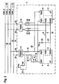
- the control unit 1 comprises a first computing device 2, which is designed as a microprocessor, and a second computing device 3, which is likewise designed as a microprocessor. On the computing devices 2, 3 computer programs are processed, so that the computing devices 2, 3 can fulfill certain control and / or locking functions.
- a preferred application of the control unit 1 is, for example, the automotive sector.
- the first computing device 2, for example, the control and / or regulation of an internal combustion engine and the second computing device 3 take over the control and / or regulation of a transmission.
- Each of the two computing devices 2, 3 has two separate data bus controllers 4, 5 and 6, 7.
- the first data bus controller 4 of the first computing device 2 comprises a first transmission terminal TxD1 and a first Reception RxD1 on.
- the second data bus controller 5 of the first computing device 2 comprises a second transmission port TxD2 and a second reception port RxD2.
- the connections TxD1 of the first data bus controllers 4, 6 of the two computing devices 2, 3 are designed as push-pull outputs, so-called push-pull connections.
- the two connections TxD2 and RxD2 of the second data bus controllers 5, 7 of the two computing devices 2, 3 are designed as open collector connections, so-called open collector connections.
- the two computing devices 2, 3 communicate with each other via an internal data bus 8.
- the internal data bus 8 comprises a first line 9, which interconnects the transmission connections TxD2 of the second data bus controllers 5, 7 of the two computing devices 2, 3, and a second line 10, which receives the reception connections RxD2 of the second data bus controllers 5, 7 both computing devices 2, 3 interconnects. Due to the relatively short length of the lines 9, 10, the lower transmission speed between the two computing devices 2, 3 via the internal data bus 8 and the almost nonexistent interferers (potential and / or level shifter) can on the use of separate transceiver units (so-called transceiver), via which the computing devices 2, 3 can be connected to the lines 9, 10, are dispensed with.
- the data transmission via the internal data bus 8 takes place according to a specific transmission protocol, for example according to the CAN (Controller Area Network) standard.
- the control unit 1 also comprises two transceiver units (transceivers) 11, 12.
- the transceivers 11, 12 are connected to an external data bus 13, which is designed as a CAN bus with two lines 14, 15 (CAN_H, CAN_L).
- the transceivers 11, 12 are for conditioning signals received from or to be sent over the external data bus 13.
- the two computing devices 2, 3 are connected to the first transceiver 11 such that both computing devices 2, 3 are connected to the external data bus 13 via this one transceiver 11.
- the first transmission connections TxD1 of the first data bus controllers 4, 6 of the two computing devices 2, 3 are routed to the inputs of an AND gate 16.
- the output of the AND gate 16 is fed via a first resistor 17 to a first terminal of the transceiver 11.
- a bridge element 18 is arranged from the first transmission terminal TxD1 of the first data bus controller 4 of the first computing device 2 to the output of the AND gate 16.
- the second terminal of the transceiver 11 is connected via a second resistor 19 to the first receiving terminal RxD1 of the first data bus controller 4 of the first computing device 2 and a second bridge element 20 to the first receiving terminal RxD1 of the first data bus controller 6 of the second computing device 3.
- At the output of the AND gate 16 is a dominant signal level when the first computing device 2 or the second computing device 3 emits a dominant signal level, or when both computing devices 2, 3 emit a dominant signal level. There is no dominant signal level only if both computing devices 2, 3 are inactive. In this respect, therefore, the signals to be transmitted from both computing devices 2, 3 are forwarded via the transceiver 11 to the external data bus 13. Signals received from the data bus 13 are routed via the transceiver 11 to both computing devices 2, 3.
- the first bridge element 18 must be open and the second bridge element 20 must be closed. Since each data bus controller 4 to 7 can only manage a limited number of message objects, so-called message objects, the first embodiment of the inventive control device 1 described has the advantage that the control device 1 has twice the number of message objects on the external data bus 13, since the two data bus controllers 4, 6 can each manage the usual number of messages, that is to say twice as many messages, on the external data bus 13.
- the second computing device 3 it is also conceivable for the second computing device 3 to transmit information to be transmitted via the external data bus 13 first to the first computing device 2 via the internal data bus 8, which then forwards the information to the external data bus 13 via the first transceiver 11 , In this case, the computing device 2 would thus effectively work as a pass-through station.
- a third bridge element 21 arranged between the two lines 9, 10 of the internal data bus 8 must be closed. Both lines 9, 10 of the internal data bus 8 are connected via a pull-up resistor 22 to a supply voltage Vcc, which may be, for example, 1.8 volts, 3.3 volts or 5.0 volts connected.
- signals on lines 9, 10 connected to open collector terminals TxD2 and RxD2 can be set to a high (1.8 volts, 3.3 volts, 5.0 volts or other Tension).
- This purpose is also served by the two pull-up resistors 23 and 24, via which the computing device side terminals of the transceiver 11 are connected to the supply voltage Vcc.
- the second computing device 3 is connected according to a third embodiment via its own transceiver to the external data bus 13.
- the terminals TxD1 and RxD1 of the first data bus controller 6 of the second computing device 3 via a third resistor 25 and a fourth resistor 26, which serve as bridges, connected to the computing device side terminals of the second transceiver 12.
- the internal data bus 8 may be placed on the external data bus 13.
- the two lines 9, 10 of the internal data bus 8 are connected via a fifth resistor 27 and a sixth resistor 28 to the computer-side connections of the second transceiver 12 according to a fourth embodiment.
- the information transfer made via the internal data bus 8 can be monitored and analyzed from outside the control unit 1 via the external data bus 13.
- the third bridge element 21 must be opened.
- An essential part of the control device 1 according to the invention is a data bus interface, which is provided by the two transceivers 11, 12 and those parts of the computing devices 2, 3, which are responsible for the communication with the internal data bus 8 and the external data bus 13.
- the computing devices 2, 3 Apart from these parts for the communication, which together with the required interconnection form the data bus interface, the computing devices 2, 3 also have parts to fulfill their intended control and / or regulating function. For example, these parts operate the control program on the computing devices 2, 3.
- FIG. 2 an inventive control device 1 according to a second preferred embodiment is shown.
- the actual circuit of the data bus interface is identical to the one in FIG. 1 illustrated circuit.
- the control unit 1 in FIG. 2 connected to two different external data buses.
- the first transceiver 11 is connected to a first data bus 13 with the lines 14, 15 (CAN_H, CAN_L).
- the second transceiver 12 is connected to a second external data bus 29 with the lines 30, 31 (CAN_H, CAN_L).
- information is transmitted via both external data buses 13, 29 according to the same transmission protocol, namely the CAN standard.
- the information can be transmitted via the two external data buses 13, 29 with the same or different data transmission rates. All above from the first embodiment of FIG. 1 described embodiments can also in the in FIG. 2 illustrated embodiment can be realized.
- the first computing device 2 transmits and receives data via the first external data bus 13, and the second computing device 3 transmits and receives data via the second external data bus 29.
- the information transmission between the two computing devices 2, 3 can be guided via the internal data bus 8 via the second transceiver 12 to the outside to the second external data bus 29 and monitored via this.
- control unit 1 With the aid of the multifunctional data bus interface according to the invention, a multiplicity of tasks and functionalities can be achieved in the control unit 1:
- the electronic circuit for the internal data bus 8 is a communication of the two computing devices 2, 3 (micro-controller) in the control unit 1 via the internal data bus 8 with transfer rates of up to 500 kBaud possible.
- the data bus 8 is also referred to as an in-house CAN bus or as an ECU-internal CAN bus. If desired, and no connection to ECU terminals 32 of the control unit 1 is created, the data exchange of the two computing devices 2, 3 is completely discrete and outside the control unit 1 is not detected.
- the internal data bus 8 is fully monitorable with appropriate component assembly with external, freely available data bus diagnostic tools. Software developers can thus efficiently verify their software, in particular the exchange of information on the internal data bus 8 perform.
- the internal data bus 8 can be connected to an external control data bus 13 or 29 via the control unit terminals 32. This eliminates the construction of other adapter boards for application purposes.
- the internal data bus 8 is connected to an external data bus 13, 29, for example, with the aim to operate monitoring and communication with other microprocessors in other control devices.
- control unit 1 according to the invention has been described for two computing devices 2, 3 and for two transceivers 11, 12. Of course, it is possible to implement the control device according to the invention with more than two computing devices and with more than two transceivers.
Landscapes
- Engineering & Computer Science (AREA)
- Theoretical Computer Science (AREA)
- Physics & Mathematics (AREA)
- General Engineering & Computer Science (AREA)
- General Physics & Mathematics (AREA)
- Small-Scale Networks (AREA)
- Bus Control (AREA)
- Multi Processors (AREA)
- Control Of Electric Motors In General (AREA)
Claims (12)
- Interface de bus de données pour appareil de commande (1), l'interface comprenant :- deux appareils de calcul (2, 3), en particulier deux microprocesseurs, qui communiquent l'un avec l'autre par un bus interne de données (8) et- deux unités d'émission-réception (11, 12) ("transceivers") raccordées à un même bus externe de données (13) ou à deux bus externes de données (13, 29) différents et raccordées aux deux appareils de calcul (2, 3) de telle sorte que les appareils de calcul (2, 3) soient raccordés au même bus externe de données (13) ou aux deux bus de données (13, 29) différents,caractérisée en ce que
une borne de réception (RxD1) du deuxième appareil de calcul (3) est raccordée par un deuxième élément de pont (20) à un conducteur qui raccorde une borne de réception (RxD1) du premier appareil de calcul (2) à la deuxième borne de l'unité (11) d'émission et de réception et
en ce que si les deux appareils de calcul (2, 3) sont raccordés au même bus externe de données (13), le deuxième élément de pont est fermé et si les deux appareils de calcul sont raccordés aux deux bus de données (13, 29) différents, le deuxième élément de pont est ouvert. - Interface de bus de données selon la revendication 1, caractérisée en ce que le bus interne de données (8) comprend deux conducteurs (9, 10) qui sont raccordés sans unités d'émission et de réception ("transceivers") aux deux appareils de calcul (2, 3).
- Interface de bus de données selon la revendication 2, caractérisée en ce que les conducteurs (9, 10) du bus interne de données (8) sont raccordés par des bornes de collecteur ouvert aux deux appareils de calcul (2, 3).
- Interface de bus de données selon l'une des revendications 1 à 3, caractérisée en ce que les deux appareils de calcul (2, 3) sont raccordés aux unités d'émission et de réception (11, 12) par des bornes dites "push-pull".
- Interface de bus de données selon l'une des revendications 1 à 4, caractérisée en ce qu'une première borne (TxD1) de chacun des deux appareils de calcul (2, 3) est raccordée par une grille ET (16) à une première borne de l'une des deux unités d'émission et de réception (11).
- Interface de bus de données selon l'une des revendications 1 à 5, caractérisée en ce qu'une deuxième borne (RxD1) de chacun des deux appareils de calcul (2, 3) est raccordée directement à une deuxième borne de l'unité d'émission et de réception (11).
- Interface de bus de données selon les revendications 5 ou 6, caractérisée en ce qu'un premier élément de pont (18) est disposé parallèlement à la grille ET (16) entre la première borne (TxD1) du premier appareil de calcul (2) et la première borne de l'unité d'émission et de réception (11).
- Interface de bus de données selon l'une des revendications 1 à 7, caractérisée en ce que le bus interne de données (8) est raccordé par l'intermédiaire d'un élément de commutation (21) à l'une des deux unités d'émission et de réception (12) et en ce qu'une liaison entre le bus interne de données (8) et l'une (12) des unités d'émission et de réception peut être établie ou interrompue au moyen de l'élément de commutation (21).
- Interface de bus de données selon la revendication 8, caractérisée en ce que l'élément de commutation (21) est configuré comme troisième élément de pont formé entre les deux conducteurs (9, 10) du bus interne de données (8).
- Interface de bus de données selon l'une des revendications 1 à 9, caractérisée en ce que le bus interne de données travaille selon la norme dite "Controller-Area-Network" (CAN).
- Interface de bus de données selon l'une des revendications 1 à 10, caractérisée en ce qu'au moins l'un des bus externes de données (13, 29) travaille selon la norme Controller-Area-Network (CAN).
- Appareil de commande (1) doté d'une interface de bus de données qui donne l'accès à un bus de données (13, 29) en vue d'établir la communication avec un autre appareil de commande par le bus de données (13, 29),
caractérisé en ce que
l'appareil de commande (1) présente une interface de bus de données selon l'une des revendications précédentes.
Applications Claiming Priority (1)
| Application Number | Priority Date | Filing Date | Title |
|---|---|---|---|
| DE102004042380A DE102004042380A1 (de) | 2004-09-02 | 2004-09-02 | Datenbus-Interface für ein Steuergerät und Steuergerät mit einem Datenbus-Interface |
Publications (3)
| Publication Number | Publication Date |
|---|---|
| EP1632865A2 EP1632865A2 (fr) | 2006-03-08 |
| EP1632865A3 EP1632865A3 (fr) | 2008-02-20 |
| EP1632865B1 true EP1632865B1 (fr) | 2010-05-19 |
Family
ID=35501021
Family Applications (1)
| Application Number | Title | Priority Date | Filing Date |
|---|---|---|---|
| EP05106497A Not-in-force EP1632865B1 (fr) | 2004-09-02 | 2005-07-14 | Interface de bus de données pour un appareil de commande et un appareil de commande avec une interface de bus de données |
Country Status (5)
| Country | Link |
|---|---|
| US (1) | US7594054B2 (fr) |
| EP (1) | EP1632865B1 (fr) |
| CN (1) | CN100538677C (fr) |
| AT (1) | ATE468563T1 (fr) |
| DE (2) | DE102004042380A1 (fr) |
Cited By (1)
| Publication number | Priority date | Publication date | Assignee | Title |
|---|---|---|---|---|
| US10291281B2 (en) | 2015-07-09 | 2019-05-14 | Continental Automotive France | Transmitter-receiver device connectable to a communications network by a CAN-type or FlexRay-type bus |
Families Citing this family (15)
| Publication number | Priority date | Publication date | Assignee | Title |
|---|---|---|---|---|
| DE102005018837A1 (de) * | 2005-04-22 | 2006-10-26 | Robert Bosch Gmbh | Verfahren und Vorrichtung zur Synchronisation zweier Bussysteme sowie Anordnung aus zwei Bussystemen |
| DE102005048585A1 (de) * | 2005-10-06 | 2007-04-12 | Robert Bosch Gmbh | Teilnehmer und Kommunikationscontroller eines Kommunikationssystems und Verfahren zur Realisierung einer Gateway-Funktionalität in einem Teilnehmer eines Kommunikationssystems |
| CN100562003C (zh) * | 2006-09-01 | 2009-11-18 | 杭州中导科技开发有限公司 | 汽车行驶记录仪can总线适配器 |
| US20110022766A1 (en) * | 2007-01-17 | 2011-01-27 | Continental Teves Ag & Co. Ohg | Circuit Arrangement For A Motor Vehicle Data Bus |
| DE102009000585B4 (de) * | 2009-02-03 | 2023-04-27 | Robert Bosch Gmbh | Synchronisierung zweier Kommunikationsnetzwerke eines elektronischen Datenverarbeitungssystems |
| JP2012235427A (ja) * | 2011-05-09 | 2012-11-29 | Denso Corp | バスコントローラの接続方法および通信システム |
| CN104301191A (zh) * | 2013-06-05 | 2015-01-21 | 上海联影医疗科技有限公司 | 总线系统 |
| WO2015045338A1 (fr) * | 2013-09-30 | 2015-04-02 | パナソニックIpマネジメント株式会社 | Appareil de communication, et appareil de commande de moteur |
| JP6421920B2 (ja) * | 2014-09-03 | 2018-11-14 | カシオ計算機株式会社 | 表示装置及びその表示制御方法、制御プログラム |
| JP6895101B2 (ja) * | 2015-12-22 | 2021-06-30 | カシオ計算機株式会社 | 表示モジュール、表示装置及びその制御方法、制御プログラム |
| JP7136893B2 (ja) * | 2018-06-14 | 2022-09-13 | 日立Astemo株式会社 | ゲートウェイ装置 |
| CN108920398B (zh) * | 2018-07-05 | 2021-01-19 | 苏州浪潮智能科技有限公司 | 一种跳帽电路及其设计方法 |
| CN209351354U (zh) * | 2018-09-28 | 2019-09-06 | 深圳市道通科技股份有限公司 | Can电路结构及其车辆诊断设备 |
| CN110221536A (zh) * | 2019-05-30 | 2019-09-10 | 中车青岛四方机车车辆股份有限公司 | 一种车门控制器 |
| DE102020200803A1 (de) * | 2020-01-23 | 2021-07-29 | Robert Bosch Gesellschaft mit beschränkter Haftung | Sende-/Empfangseinrichtung und Kommunikationssteuereinrichtung für eine Teilnehmerstation eines seriellen Bussystems und Verfahren zur Kommunikation in einem seriellen Bussystem |
Family Cites Families (19)
| Publication number | Priority date | Publication date | Assignee | Title |
|---|---|---|---|---|
| US3569847A (en) * | 1969-06-23 | 1971-03-09 | Lockheed Aircraft Corp | Amplifier system for driving shaker motors |
| US4253179A (en) * | 1977-08-17 | 1981-02-24 | Nippon Electric Co., Ltd. | Time division digital switching system with code converting and inverse-converting circuits |
| US4542502A (en) * | 1983-12-30 | 1985-09-17 | At&T Bell Laboratories | Reconfigurable collision avoiding system, station and protocol for a two path multiple access digital communications system |
| NL8700736A (nl) * | 1987-03-30 | 1988-10-17 | Philips Nv | Een-kanaalsbussysteem voor meermeester gebruik, met bitcelsynchronisatie, en meesterstation voorzien van een bitcelsynchronisatie-element daarvoor. |
| DE3730468A1 (de) * | 1987-09-08 | 1989-03-16 | Bergmann Kabelwerke Ag | Bordnetz fuer kraftfahrzeuge und verfahren zum betrieb des bordnetzes |
| IT1232089B (it) * | 1989-05-04 | 1992-01-23 | Sgs Thomson Microelectronics | Sistema di comunicazione tra un unita di elaborazione principale e delle unita periferiche |
| JP2851124B2 (ja) * | 1990-04-27 | 1999-01-27 | 古河電気工業株式会社 | 多重伝送方式 |
| US5187709A (en) * | 1990-05-08 | 1993-02-16 | Caterpillar Inc. | Fault tolerant serial communications network |
| DE69231452T2 (de) * | 1991-01-25 | 2001-05-03 | Hitachi Ltd | Fehlertolerantes Rechnersystem mit Verarbeitungseinheiten die je mindestens drei Rechnereinheiten haben |
| US5214582C1 (en) * | 1991-01-30 | 2001-06-26 | Edge Diagnostic Systems | Interactive diagnostic system for an automobile vehicle and method |
| US5274636A (en) * | 1992-04-20 | 1993-12-28 | Chrysler Corporation | Automatic multiplex data link system, symbol encoder decoder therefor |
| DE19509558A1 (de) * | 1995-03-16 | 1996-09-19 | Abb Patent Gmbh | Verfahren zur fehlertoleranten Kommunikation unter hohen Echtzeitbedingungen |
| WO1998044469A2 (fr) * | 1997-03-27 | 1998-10-08 | Elan Schaltelemente Gmbh | Systeme de commande de securite et procede pour la mise en oeuvre d'un tel systeme |
| US5900017A (en) * | 1997-05-14 | 1999-05-04 | International Business Machines Corporation | Snooping a variable number of cache addresses in a multiple processor system by a single snoop request |
| US5995376A (en) * | 1997-05-20 | 1999-11-30 | National Instruments Corporation | Chassis which includes configurable slot 0 locations |
| EP0881572B1 (fr) * | 1997-05-28 | 2001-10-10 | Agilent Technologies, Inc. (a Delaware corporation) | Surveillance permanente de pannes dans des systèmes complexes |
| GB2345153A (en) * | 1998-12-23 | 2000-06-28 | Motorola Ltd | Fault-tolerant microcontroller arrangement, eg for a vehicle braking system |
| DE20217059U1 (de) * | 2002-11-04 | 2003-01-16 | Raytheon Marine Gmbh | Kompass mit elektromagnetischer Halbschalentransformator-Energieübertragung und optoelektronischer Datensignalübertragung |
| CN2638141Y (zh) * | 2003-08-29 | 2004-09-01 | 清华大学 | 基于cf卡的便携式can总线分析记录仪 |
-
2004
- 2004-09-02 DE DE102004042380A patent/DE102004042380A1/de not_active Ceased
-
2005
- 2005-07-14 AT AT05106497T patent/ATE468563T1/de not_active IP Right Cessation
- 2005-07-14 DE DE502005009586T patent/DE502005009586D1/de active Active
- 2005-07-14 EP EP05106497A patent/EP1632865B1/fr not_active Not-in-force
- 2005-08-29 US US11/215,706 patent/US7594054B2/en active Active
- 2005-09-02 CN CNB2005100996827A patent/CN100538677C/zh not_active Expired - Fee Related
Cited By (1)
| Publication number | Priority date | Publication date | Assignee | Title |
|---|---|---|---|---|
| US10291281B2 (en) | 2015-07-09 | 2019-05-14 | Continental Automotive France | Transmitter-receiver device connectable to a communications network by a CAN-type or FlexRay-type bus |
Also Published As
| Publication number | Publication date |
|---|---|
| US7594054B2 (en) | 2009-09-22 |
| DE502005009586D1 (de) | 2010-07-01 |
| DE102004042380A1 (de) | 2006-03-09 |
| EP1632865A3 (fr) | 2008-02-20 |
| CN100538677C (zh) | 2009-09-09 |
| EP1632865A2 (fr) | 2006-03-08 |
| ATE468563T1 (de) | 2010-06-15 |
| CN1744066A (zh) | 2006-03-08 |
| US20060106966A1 (en) | 2006-05-18 |
Similar Documents
| Publication | Publication Date | Title |
|---|---|---|
| EP1632865B1 (fr) | Interface de bus de données pour un appareil de commande et un appareil de commande avec une interface de bus de données | |
| EP1566029B1 (fr) | Unite de passerelle permettant de connecter des sous-reseaux, notamment dans des vehicules | |
| EP3523930B1 (fr) | Véhicule à moteur muni d'un réseau de données interne au véhicule ainsi que procédé de fonctionnement du véhicule à moteur | |
| DE10211939A1 (de) | Kopplungsvorrichtung zum Ankoppeln von Geräten an ein Bussystem | |
| DE102011114077A1 (de) | PLC System | |
| DE10153085A1 (de) | Verfahren und Vorrichtung zur Programmierung einer Steuereinheit | |
| EP3575899B1 (fr) | Système d'automatisation, procédé de fonctionnement pour système d'automatisation et produit de programme informatique | |
| EP2093941A1 (fr) | Système de bus de terrain | |
| EP2491492A1 (fr) | Système d'automatisation et procédé pour faire fonctionner un système d'automatisation | |
| EP2165474A2 (fr) | Redondance cyclique rapide d'un réseau | |
| EP3381159B1 (fr) | Accès direct aux signaux de bus dans un véhicule à moteur | |
| WO2012110541A1 (fr) | Procédé de transmission de données par le biais d'un bus de données série synchrone | |
| DE102011107322A1 (de) | Kommunikationsschnittstellenmodul für ein Automatisierungssystem | |
| DE112012003005T5 (de) | Netzwerk für die Übertragung von Informationen und entsprechender Netzwerkknoten | |
| EP3772206A1 (fr) | Adaptateur de réseau destiné au transfert unidirectionnel de données | |
| DE60319175T2 (de) | Datenübertragungssystem im Fahrzeug mit redundanten Verbindungen | |
| DE102004054016A1 (de) | Steuergerät zum Steuern und/oder regeln mindestens einer Fahrzeugfunktion | |
| DE102004002330A1 (de) | System zur Datenübertragung in Schaltanlagen | |
| EP3632054B1 (fr) | Determination de noeuds d'un bus de données local | |
| DE10239846B4 (de) | Fail-Silent-Steuergerät | |
| DE102019200907A1 (de) | Teilnehmerstation für ein Bussystem und Verfahren zur Datenübertragung in einem Bussystem | |
| DE102011005239A1 (de) | Sicherheitssystem sowie Verfahren zum Austauschen von sicherheitsgerichteten Daten in einem Sicherheitssystem | |
| EP1629637B1 (fr) | Transmission de messages dans un systeme temps reel temporise distribue | |
| DE102012201669B4 (de) | Verfahren und Kommunikationscontroller zur Datenübertragung zwischen zwei mittels Übertragungsstrecken verbundenen Datenverarbeitungseinheiten | |
| EP3236637B1 (fr) | Communication par l'intermediaire d'un réseau de trafic à grande distance à l'aide d'un protocole d'application spécifique |
Legal Events
| Date | Code | Title | Description |
|---|---|---|---|
| PUAI | Public reference made under article 153(3) epc to a published international application that has entered the european phase |
Free format text: ORIGINAL CODE: 0009012 |
|
| AK | Designated contracting states |
Kind code of ref document: A2 Designated state(s): AT BE BG CH CY CZ DE DK EE ES FI FR GB GR HU IE IS IT LI LT LU LV MC NL PL PT RO SE SI SK TR |
|
| AX | Request for extension of the european patent |
Extension state: AL BA HR MK YU |
|
| PUAL | Search report despatched |
Free format text: ORIGINAL CODE: 0009013 |
|
| AK | Designated contracting states |
Kind code of ref document: A3 Designated state(s): AT BE BG CH CY CZ DE DK EE ES FI FR GB GR HU IE IS IT LI LT LU LV MC NL PL PT RO SE SI SK TR |
|
| AX | Request for extension of the european patent |
Extension state: AL BA HR MK YU |
|
| 17P | Request for examination filed |
Effective date: 20080820 |
|
| AKX | Designation fees paid |
Designated state(s): AT BE BG CH CY CZ DE DK EE ES FI FR GB GR HU IE IS IT LI LT LU LV MC NL PL PT RO SE SI SK TR |
|
| GRAP | Despatch of communication of intention to grant a patent |
Free format text: ORIGINAL CODE: EPIDOSNIGR1 |
|
| GRAS | Grant fee paid |
Free format text: ORIGINAL CODE: EPIDOSNIGR3 |
|
| GRAA | (expected) grant |
Free format text: ORIGINAL CODE: 0009210 |
|
| AK | Designated contracting states |
Kind code of ref document: B1 Designated state(s): AT BE BG CH CY CZ DE DK EE ES FI FR GB GR HU IE IS IT LI LT LU LV MC NL PL PT RO SE SI SK TR |
|
| REG | Reference to a national code |
Ref country code: GB Ref legal event code: FG4D Free format text: NOT ENGLISH |
|
| REG | Reference to a national code |
Ref country code: CH Ref legal event code: EP |
|
| REG | Reference to a national code |
Ref country code: IE Ref legal event code: FG4D Free format text: LANGUAGE OF EP DOCUMENT: GERMAN |
|
| REF | Corresponds to: |
Ref document number: 502005009586 Country of ref document: DE Date of ref document: 20100701 Kind code of ref document: P |
|
| REG | Reference to a national code |
Ref country code: NL Ref legal event code: VDEP Effective date: 20100519 |
|
| LTIE | Lt: invalidation of european patent or patent extension |
Effective date: 20100519 |
|
| PG25 | Lapsed in a contracting state [announced via postgrant information from national office to epo] |
Ref country code: ES Free format text: LAPSE BECAUSE OF FAILURE TO SUBMIT A TRANSLATION OF THE DESCRIPTION OR TO PAY THE FEE WITHIN THE PRESCRIBED TIME-LIMIT Effective date: 20100830 Ref country code: SE Free format text: LAPSE BECAUSE OF FAILURE TO SUBMIT A TRANSLATION OF THE DESCRIPTION OR TO PAY THE FEE WITHIN THE PRESCRIBED TIME-LIMIT Effective date: 20100519 Ref country code: LT Free format text: LAPSE BECAUSE OF FAILURE TO SUBMIT A TRANSLATION OF THE DESCRIPTION OR TO PAY THE FEE WITHIN THE PRESCRIBED TIME-LIMIT Effective date: 20100519 |
|
| PG25 | Lapsed in a contracting state [announced via postgrant information from national office to epo] |
Ref country code: SI Free format text: LAPSE BECAUSE OF FAILURE TO SUBMIT A TRANSLATION OF THE DESCRIPTION OR TO PAY THE FEE WITHIN THE PRESCRIBED TIME-LIMIT Effective date: 20100519 Ref country code: LV Free format text: LAPSE BECAUSE OF FAILURE TO SUBMIT A TRANSLATION OF THE DESCRIPTION OR TO PAY THE FEE WITHIN THE PRESCRIBED TIME-LIMIT Effective date: 20100519 Ref country code: IS Free format text: LAPSE BECAUSE OF FAILURE TO SUBMIT A TRANSLATION OF THE DESCRIPTION OR TO PAY THE FEE WITHIN THE PRESCRIBED TIME-LIMIT Effective date: 20100919 Ref country code: FI Free format text: LAPSE BECAUSE OF FAILURE TO SUBMIT A TRANSLATION OF THE DESCRIPTION OR TO PAY THE FEE WITHIN THE PRESCRIBED TIME-LIMIT Effective date: 20100519 |
|
| PG25 | Lapsed in a contracting state [announced via postgrant information from national office to epo] |
Ref country code: CY Free format text: LAPSE BECAUSE OF FAILURE TO SUBMIT A TRANSLATION OF THE DESCRIPTION OR TO PAY THE FEE WITHIN THE PRESCRIBED TIME-LIMIT Effective date: 20100519 Ref country code: PL Free format text: LAPSE BECAUSE OF FAILURE TO SUBMIT A TRANSLATION OF THE DESCRIPTION OR TO PAY THE FEE WITHIN THE PRESCRIBED TIME-LIMIT Effective date: 20100519 Ref country code: GR Free format text: LAPSE BECAUSE OF FAILURE TO SUBMIT A TRANSLATION OF THE DESCRIPTION OR TO PAY THE FEE WITHIN THE PRESCRIBED TIME-LIMIT Effective date: 20100820 |
|
| REG | Reference to a national code |
Ref country code: IE Ref legal event code: FD4D |
|
| BERE | Be: lapsed |
Owner name: ROBERT BOSCH G.M.B.H. Effective date: 20100731 |
|
| PG25 | Lapsed in a contracting state [announced via postgrant information from national office to epo] |
Ref country code: PT Free format text: LAPSE BECAUSE OF FAILURE TO SUBMIT A TRANSLATION OF THE DESCRIPTION OR TO PAY THE FEE WITHIN THE PRESCRIBED TIME-LIMIT Effective date: 20100920 Ref country code: NL Free format text: LAPSE BECAUSE OF FAILURE TO SUBMIT A TRANSLATION OF THE DESCRIPTION OR TO PAY THE FEE WITHIN THE PRESCRIBED TIME-LIMIT Effective date: 20100519 Ref country code: IE Free format text: LAPSE BECAUSE OF FAILURE TO SUBMIT A TRANSLATION OF THE DESCRIPTION OR TO PAY THE FEE WITHIN THE PRESCRIBED TIME-LIMIT Effective date: 20100519 Ref country code: DK Free format text: LAPSE BECAUSE OF FAILURE TO SUBMIT A TRANSLATION OF THE DESCRIPTION OR TO PAY THE FEE WITHIN THE PRESCRIBED TIME-LIMIT Effective date: 20100519 Ref country code: EE Free format text: LAPSE BECAUSE OF FAILURE TO SUBMIT A TRANSLATION OF THE DESCRIPTION OR TO PAY THE FEE WITHIN THE PRESCRIBED TIME-LIMIT Effective date: 20100519 |
|
| PG25 | Lapsed in a contracting state [announced via postgrant information from national office to epo] |
Ref country code: RO Free format text: LAPSE BECAUSE OF FAILURE TO SUBMIT A TRANSLATION OF THE DESCRIPTION OR TO PAY THE FEE WITHIN THE PRESCRIBED TIME-LIMIT Effective date: 20100519 Ref country code: MC Free format text: LAPSE BECAUSE OF NON-PAYMENT OF DUE FEES Effective date: 20100731 Ref country code: CZ Free format text: LAPSE BECAUSE OF FAILURE TO SUBMIT A TRANSLATION OF THE DESCRIPTION OR TO PAY THE FEE WITHIN THE PRESCRIBED TIME-LIMIT Effective date: 20100519 Ref country code: SK Free format text: LAPSE BECAUSE OF FAILURE TO SUBMIT A TRANSLATION OF THE DESCRIPTION OR TO PAY THE FEE WITHIN THE PRESCRIBED TIME-LIMIT Effective date: 20100519 |
|
| REG | Reference to a national code |
Ref country code: CH Ref legal event code: PL |
|
| PLBE | No opposition filed within time limit |
Free format text: ORIGINAL CODE: 0009261 |
|
| STAA | Information on the status of an ep patent application or granted ep patent |
Free format text: STATUS: NO OPPOSITION FILED WITHIN TIME LIMIT |
|
| PG25 | Lapsed in a contracting state [announced via postgrant information from national office to epo] |
Ref country code: IT Free format text: LAPSE BECAUSE OF FAILURE TO SUBMIT A TRANSLATION OF THE DESCRIPTION OR TO PAY THE FEE WITHIN THE PRESCRIBED TIME-LIMIT Effective date: 20100519 |
|
| 26N | No opposition filed |
Effective date: 20110222 |
|
| PG25 | Lapsed in a contracting state [announced via postgrant information from national office to epo] |
Ref country code: CH Free format text: LAPSE BECAUSE OF NON-PAYMENT OF DUE FEES Effective date: 20100731 Ref country code: LI Free format text: LAPSE BECAUSE OF NON-PAYMENT OF DUE FEES Effective date: 20100731 |
|
| REG | Reference to a national code |
Ref country code: DE Ref legal event code: R097 Ref document number: 502005009586 Country of ref document: DE Effective date: 20110221 |
|
| PG25 | Lapsed in a contracting state [announced via postgrant information from national office to epo] |
Ref country code: BE Free format text: LAPSE BECAUSE OF NON-PAYMENT OF DUE FEES Effective date: 20100731 |
|
| PG25 | Lapsed in a contracting state [announced via postgrant information from national office to epo] |
Ref country code: AT Free format text: LAPSE BECAUSE OF NON-PAYMENT OF DUE FEES Effective date: 20100714 |
|
| PG25 | Lapsed in a contracting state [announced via postgrant information from national office to epo] |
Ref country code: HU Free format text: LAPSE BECAUSE OF FAILURE TO SUBMIT A TRANSLATION OF THE DESCRIPTION OR TO PAY THE FEE WITHIN THE PRESCRIBED TIME-LIMIT Effective date: 20101120 Ref country code: LU Free format text: LAPSE BECAUSE OF NON-PAYMENT OF DUE FEES Effective date: 20100714 Ref country code: BG Free format text: LAPSE BECAUSE OF FAILURE TO SUBMIT A TRANSLATION OF THE DESCRIPTION OR TO PAY THE FEE WITHIN THE PRESCRIBED TIME-LIMIT Effective date: 20100519 |
|
| PG25 | Lapsed in a contracting state [announced via postgrant information from national office to epo] |
Ref country code: TR Free format text: LAPSE BECAUSE OF FAILURE TO SUBMIT A TRANSLATION OF THE DESCRIPTION OR TO PAY THE FEE WITHIN THE PRESCRIBED TIME-LIMIT Effective date: 20100519 |
|
| PG25 | Lapsed in a contracting state [announced via postgrant information from national office to epo] |
Ref country code: BG Free format text: LAPSE BECAUSE OF FAILURE TO SUBMIT A TRANSLATION OF THE DESCRIPTION OR TO PAY THE FEE WITHIN THE PRESCRIBED TIME-LIMIT Effective date: 20100819 |
|
| REG | Reference to a national code |
Ref country code: FR Ref legal event code: PLFP Year of fee payment: 12 |
|
| REG | Reference to a national code |
Ref country code: FR Ref legal event code: PLFP Year of fee payment: 13 |
|
| REG | Reference to a national code |
Ref country code: FR Ref legal event code: PLFP Year of fee payment: 14 |
|
| PGFP | Annual fee paid to national office [announced via postgrant information from national office to epo] |
Ref country code: DE Payment date: 20200924 Year of fee payment: 16 Ref country code: GB Payment date: 20200724 Year of fee payment: 16 Ref country code: FR Payment date: 20200727 Year of fee payment: 16 |
|
| REG | Reference to a national code |
Ref country code: DE Ref legal event code: R119 Ref document number: 502005009586 Country of ref document: DE |
|
| GBPC | Gb: european patent ceased through non-payment of renewal fee |
Effective date: 20210714 |
|
| PG25 | Lapsed in a contracting state [announced via postgrant information from national office to epo] |
Ref country code: GB Free format text: LAPSE BECAUSE OF NON-PAYMENT OF DUE FEES Effective date: 20210714 Ref country code: DE Free format text: LAPSE BECAUSE OF NON-PAYMENT OF DUE FEES Effective date: 20220201 |
|
| PG25 | Lapsed in a contracting state [announced via postgrant information from national office to epo] |
Ref country code: FR Free format text: LAPSE BECAUSE OF NON-PAYMENT OF DUE FEES Effective date: 20210731 |