EP1632858B1 - Semiconductor memory device and access method and memory control system for same - Google Patents
Semiconductor memory device and access method and memory control system for same Download PDFInfo
- Publication number
- EP1632858B1 EP1632858B1 EP05291757.2A EP05291757A EP1632858B1 EP 1632858 B1 EP1632858 B1 EP 1632858B1 EP 05291757 A EP05291757 A EP 05291757A EP 1632858 B1 EP1632858 B1 EP 1632858B1
- Authority
- EP
- European Patent Office
- Prior art keywords
- semiconductor memory
- region
- memory
- cache
- address
- Prior art date
- Legal status (The legal status is an assumption and is not a legal conclusion. Google has not performed a legal analysis and makes no representation as to the accuracy of the status listed.)
- Expired - Lifetime
Links
Images




Classifications
-
- G—PHYSICS
- G11—INFORMATION STORAGE
- G11C—STATIC STORES
- G11C16/00—Erasable programmable read-only memories
-
- G—PHYSICS
- G06—COMPUTING OR CALCULATING; COUNTING
- G06F—ELECTRIC DIGITAL DATA PROCESSING
- G06F12/00—Accessing, addressing or allocating within memory systems or architectures
- G06F12/02—Addressing or allocation; Relocation
- G06F12/08—Addressing or allocation; Relocation in hierarchically structured memory systems, e.g. virtual memory systems
- G06F12/0802—Addressing of a memory level in which the access to the desired data or data block requires associative addressing means, e.g. caches
-
- G—PHYSICS
- G06—COMPUTING OR CALCULATING; COUNTING
- G06F—ELECTRIC DIGITAL DATA PROCESSING
- G06F12/00—Accessing, addressing or allocating within memory systems or architectures
- G06F12/02—Addressing or allocation; Relocation
- G06F12/0223—User address space allocation, e.g. contiguous or non contiguous base addressing
- G06F12/023—Free address space management
- G06F12/0238—Memory management in non-volatile memory, e.g. resistive RAM or ferroelectric memory
- G06F12/0246—Memory management in non-volatile memory, e.g. resistive RAM or ferroelectric memory in block erasable memory, e.g. flash memory
Definitions
- the present invention relates to a semiconductor memory device, more particularly relates to a semiconductor memory device having a built-in cache memory and an access method and a memory control system for the same.
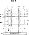
- FIG. 1 is a view of an example of the internal configuration of an example of a block access type memory, that is, a NAND type flash memory.
- the NAND type flash memory of FIG. 1 has a plurality of memory units 1-1 to 1-n connected to bit lines BL1 to BLn and arrayed in an array (vertically and laterally).
- the memory units 1 (-1 to -n) are sandwiched between selection transistors 2 and 3 and include for example 16 memory cells N0 to N15 connected in series.
- gates of the selection transistors 2 and 3 in odd number columns are connected to selection gate lines SL1 and SL2, while gates of the selection transistors 2 and 3 in even number columns are connected to selection gate lines SL3 and SL4.
- the gates of the memory cells N0 to N15 are connected to word lines WL0 to WL15.
- the memory cells N0 to N15 have multilayer gate structures and store data according to the charges built up in the floating gates. Namely, when many electrons build up in a floating gate, the threshold value of the transistor rises, therefore any current penetration through the memory units 1 (-1 to -n) from the charged bit lines BL1 to BLn is detected at an access circuit 4 including a sense amplifier etc. and the data judged.
- the data of the large number of cells connected to a selected word line in the array is simultaneously read out by the sense amplifier in parallel. Therefore, an increase in speed is possible in block units of several kB. Namely, once header data is read, continuous data can be read at a high speed.
- the speed of write operations can be similarly increased by the same parallel processing.
- a NAND type flash memory a low current write operation by Fowler-Nordheim (F-N) injection is possible. Therefore, the speed of transfer in block units is faster than the speed of NOR type flash memories by close to 2 orders.
- F-N Fowler-Nordheim
- Such a memory is mainly used as a user file storage for portable phones, digital cameras, etc. at present.
- FIG. 2 is a block diagram conceptually showing the system configuration when using flash memories for user file storage.
- This system 10 is comprised of a central processing unit (CPU) 11, a NOR type flash memory 13, and a dynamic random access memory (DRAM) 14 connected via a system bus 12. Both memories are mapped as regions in the system memory.
- the NOR type flash memory 13 stores the boot code, operating system (OS), and applications. Further, the DRAM 14 is loaded with part of the applications for execution and forms a work area of the OS.
- the system bus 12 is further connected to an interface circuit (IF) 15 for accessing an external memory device and the interface circuit 15 is connected to a control circuit 16 for controlling a NAND type flash memory 17.
- the control circuit 16 inputs/outputs and transfers data of the NAND type flash memory 17 matched with the specifications of the interface circuit 15 determined by ATA standard etc. and further has a function of converting a logical address designated from the outside to a physical address of the memory 17, a function of encoding and correcting errors of the data read out from the memory 17 at an ECC circuit, and other functions.
- FIG. 3 is a view of an example of a memory map of the system of FIG. 2 .
- 21 indicates the memory region of the NOR type flash memory 13
- 22 indicates the memory region of the DRAM 14.
- the CPU 11 accesses the NOR type flash memory region 21 first and executes the boot code 23 thereof.
- various types of programs are loaded into the DRAM region 22 from the NOR type flash memory region 21 for execution.
- driver software 24 for operating the interface circuit 15 is loaded and executed.
- Access to the NAND type flash memory 17 becomes possible at that point of time.
- the flash memory 17 is not mapped to the system memory.
- An IO map space is separately provided, and data is transferred using a specific protocol prescribed by the interface circuit 15 and the driver software 24 via a register mapped there.
- block device management software 25 is loaded and executed and a block data cache region 26 is secured and managed.
- the NAND type flash memory 17 When the NAND type flash memory 17 becomes usable in this way, it is mainly used for storing user data as files. Further, parts of the applications are stored as files. These are sometimes loaded, opened up, and executed in empty regions in the DRAM 14.
- a NAND type flash memory is an inexpensive non-volatile memory, it is not suitable for random access. Further, a long time is required for acquiring the initial data. Accordingly, it cannot be accessed like a usual system memory and ends up being treated like a block access external memory device in the same way as a hard disk. As a result, the interface circuit 15 for the external memory device becomes necessary, so the mounting of the memory device and the circuit configuration of the system become more complex. Further, the driver software 24 is necessary for operation of the interface circuit 15 as explained above, and the transfer performance of the memory is restricted by its protocol.
- the host controller cannot efficiently transfer data unless a cache memory region 26 is separately provided in the system memory and managed by management software 25.
- the management software needs to perform a variety of processing such as monitoring of updating of data and further, in certain cases, providing a backup mechanism to deal with instantaneous interruptions in power. Accordingly, the host controller has to handle much additional work when handling block data, so good processing performance is hard to achieve.
- NOR type flash memory 13 can perform random read operations in units of words and can be treated as the system memory, but is expensive. Further, usually it can only be accessed as a read only memory (ROM) and cannot be treated as a random access memory (RAM). Overwriting requires exceptional operations different from ordinary access and in addition takes a very long time.
- a semiconductor memory device as set out in claim 1.
- the semiconductor device includes a first semiconductor memory and a second semiconductor memory, wherein the second semiconductor memory is a cache of the first semiconductor memory, the first semiconductor memory is accessed via the second semiconductor memory, there are a first address region and a second address region on logical memory addresses accessed from the outside, at least part of the second semiconductor memory is mapped to the first address region, and a function of controlling data transfer between the first semiconductor memory and the second semiconductor memory by accessing the second address region is provided.
- the device has a function of transferring a desired block region data in the first semiconductor memory to the second semiconductor memory in accordance with predetermined information being written to the second address region from the outside.
- the device has a function of judging whether or not the desired block region data in the first semiconductor memory is being transferred to the second semiconductor memory by predetermined data being read from the second address region.
- the first semiconductor memory is a block access type large size memory
- the second semiconductor memory is a random access type small size memory
- the data transfer between the first semiconductor memory and the second semiconductor memory is carried out in units of blocks.
- the device has a function of transferring a desired block region in the first semiconductor memory to the cache region of the second semiconductor memory in accordance with predetermined information being written into the second address region from the outside and notifying completion of the transfer to the outside when the transfer is completed.
- the first semiconductor memory is a non-volatile memory and has a function of detecting the power being turned on or a reset being input and automatically transfers and stores a predetermined region data of the first semiconductor memory to the second semiconductor memory.
- the first address region is set in one-to-once correspondence with the logical address region of the first semiconductor memory and when the first address region is accessed, the corresponding region in the first semiconductor memory is accessed via the second semiconductor memory.
- correspondence information indicating which region of the first semiconductor memory is stored in which region of the second semiconductor memory is stored, and when the first address region is accessed from the outside, the second semiconductor memory is accessed according to an internal address converted and generated from the input address and the correspondence information.
- a memory control system as set out in claim 7.
- the memory control system has a semiconductor memory device and a host device executing at least a management program to access the semiconductor memory device, wherein the semiconductor memory device includes a first semiconductor memory and a second semiconductor memory, the second semiconductor memory is the cache of the first semiconductor memory, the first semiconductor memory is accessed via the second semiconductor memory, there is a first address region and a second address region at logical memory addresses accessed from the host device, at least part of the second semiconductor memory is mapped to the first address region, functions of controlling the data transfer between the first semiconductor memory and the second semiconductor memory by accessing the second address region and transferring a desired block region data in the first semiconductor memory to the second semiconductor memory in accordance with predetermined information being written into the second address region from the host device are provided, and the host device executes a management program making the host controller write predetermined information into the second address region of the semiconductor memory device according to need when accessing the semiconductor memory device and making the semiconductor memory device transfer the desired
- the acces method of a semiconductor memory device including a first semiconductor memory and a second semiconductor memory comprising steps of accessing the first semiconductor memory via the second semiconductor memory using the second semiconductor memory as the cache of the first semiconductor memory, forming a first address region and a second address region at logical memory addresses accessed from the outside, mapping at least part of the second semiconductor memory in the first address region, and transferring data between the first semiconductor memory and the second semiconductor memory by accessing the second address region.
- the semiconductor memory device is configured by a first semiconductor memory and a second semiconductor memory, the second semiconductor memory is the cache of the first semiconductor memory, and the first semiconductor memory is accessed via the second semiconductor memory.
- the device has a randomly accessible cache region and a cache control region at logical memory addresses. At least part of the second semiconductor memory is mapped to this cache region.
- the cache control region By accessing the cache control region from the outside, data transfer between the first semiconductor memory and the second semiconductor memory is controlled.
- the desired block region in the first semiconductor memory is transferred to the cache region in accordance with predetermined information being written into the cache control region from the outside.
- the host device executes the following management program according to need when accessing the semiconductor memory device. Namely, the management program writes the address information of the desired region to the cache control region of the semiconductor memory device, makes the memory device transfer the corresponding region to the cache region, and notifies completion to the host controller when the transfer is completed.
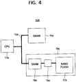
- FIG. 4 is a block diagram of a memory control system employing a semiconductor memory device according to an embodiment of the present invention.
- the system 10 has, as shown FIG. 4 , for example a host device constituted by a CPU (also referred to as a "host CPU”) 11a, a system bus 12a, a DRAM 14a, and a semiconductor memory device (hereinafter, also referred to as a "memory device”) 19a including a first semiconductor memory and a second semiconductor memory as principal components.
- a host CPU also referred to as a "host CPU”
- system bus 12a also referred to as a "DRAM 14a
- DRAM 14a DRAM
- semiconductor memory device hereinafter, also referred to as a "memory device”
- the DRAM 14a and the memory device 19a are connected to the CPU 11a via the system bus 12a.
- the memory device 19a is compatible in pins with a NOR type flash memory, and can be mounted on a general board as it is.
- the memory device 19a is configured by the second semiconductor memory constituted by a static random access memory (SRAM) 18a having a capacity of 2 Mb, a control circuit 16a, and the first semiconductor memory constituted by a NAND type flash memory 17a having a capacity of 1 Gb in the same package.
- the SRAM 18a is used as the cache of the NAND type flash memory 17a. Accordingly, in the following description, the SRAM is sometimes referred to as an "SRAM cache".
- the inside of the NAND type flash memory 17a is divided into a plurality of banks. By operating them parallel, high speed transfer of block data is possible.
- the control circuit 16a executes and controls the transfer between the SRAM 18a and the NAND type flash memory 17a as will be explained later and, in the present embodiment, is mounted on the same chip as the SRAM 18a.
- the control circuit 16a has a function of converting a logical address of the NAND type flash memory 17a to a physical address and prohibiting access to an error block, a function of encoding and correcting error of data read out from the NAND type flash memory 17a by an ECC circuit, and other functions.
- the bus width between the NAND type flash memory 17a as the main memory and the SRAM 18a as the cache memory and the transfer frequency can be uniquely set in the memory device 19a.
- packaging technology has been remarkably improved in recent years. Therefore, it is possible to arrange the two memories 17a and 18a close so as to reduce the load on the buses between the two and to make them wider than the system bus 12a or raise the frequency so as to achieve a great improvement of the transfer performance.
- FIG. 5 is a diagram showing a first example of mapping of logical addresses of the memory device 19a and logical addresses of the SRAM cache 18a and the NAND type flash memory 17a configuring the inside thereof in the present embodiment.
- 31 indicates the logical addresses of the memory device 19a
- 32 indicates the logical addresses of the SRAM cache 18a
- 33 indicates the logical addresses of the NAND type flash memory 17a.
- 34 to 36 indicate address regions of the memory device 19a
- 37 and 38 indicate address regions of the SRAM cache 18a.
- the logical addresses 31 and 32 of the memory device 19a and the SRAM cache 18a are assigned in units of words each consisting of 32 bits matching with the input/output width of the memory device, and the addresses 33 of the NAND type flash memory 17a are assigned in units of 1M bit erasure blocks.
- the address region 34 of the memory device 19a is directly mapped to the address region 37 of the SRAM 18a. When this address region is accessed from the outside, the SRAM 18a is therefore immediately accessed. On the other hand, the address region 35 of the memory device 19a is prohibited from use here and is not mapped anywhere. Further, the register 39 in the control circuit 16a is mapped to the address region 36 of the memory device 19a. By accessing this portion, it is possible to judge the internal state of the SRAM 18a and control the data transfer between the SRAM 18a and the NAND type flash memory 17a.
- the address region 37 of the SRAM 18a serves as a cache for all of the logical addresses 33 of the NAND type flash memory 17a. Namely, 1 block is selected from the region of the logical addresses 33. That group of data is transferred inside the memory device 19a at a high speed and stored in the address region 37 in the SRAM 18a. For example, when a block address "001" is written into a TAG portion 42 in the register 39 from the outside, the control circuit 16a detects that and transfers the block (40_001) to the address region 37 for storage.
- the remaining half of the address region 38 of the SRAM 18a is usually not mapped to any address region of the memory device 19a and not seen by the user, but is used as a buffer at the time of writing data or as a standby region for coping with the following case.
- the updated block data of the address region 37 of the SRAM 18a is transferred to the address region 38 as the buffer at a high speed.
- the data of the new read out block is immediately loaded in the address region 37 of the SRAM 18a from the block (40_002) of the NAND type flash memory 17a.
- the data of the old block (40_001) in the logical address 33 of the NAND type flash memory 17a is erased, and the updated data is transferred from the buffer 38 of the SRAM 18a. Due to this, even if not waiting for the erasing and writing, a user can freely access the data of the new read out block of the cache region 37.
- the region mapped to the cache region (address region) 34 of the memory device 19a from the region 37 to the region 38 of the SRAM 18a and to load the data of the new read out block (40_002) of the NAND type flash memory 17a to the region 38.
- the data of the old block (40_001) at the logical address 33 of the NAND type flash memory 17a is erased, and the updated data is transferred from the address region 37 of the SRAM 18a. Thereafter, the address region 37 of the SRAM 18a becomes a standby region.
- the memory device 19a memory accesses the address region 36 from the outside and therefore can perform various types of control such as confirmation of hits to the cache and internal transfer of desired blocks.
- various types of control such as confirmation of hits to the cache and internal transfer of desired blocks.
- the TAG portion 42 is rewritten to the desired block address.
- the control circuit 16a in the memory device 19a detects this and transfers the group of data of the desired block from the region 33 in the NAND type flash memory 17a to the region 37 in the SRAM 18a for storage.
- the transfer is completed, the fact that access from the outside is possible is notified to a status display 43 provided a part of the internal register 39.
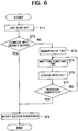
- the CPU as the host controller (hereinafter referred to as the "host CPU") 11a executes a management program as in for example FIG. 6 according to need when accessing the memory.
- This program first reads out the TAG portion 42 (ST1). When it coincides with the desired block address (ST2), it notifies access permission to the host CPU 11a (ST3). When it conversely does not coincide (ST2), the block address is written into the TAG portion 42 (ST4). The status display 43 is periodically checked after that (ST5 to ST7). When the status display 43 displays completion of the internal transfer, access permission is notified to the host controller (ST3). In this way, all of the control from the management program to the memory device 19a is executed by usual memory access to the address region 36 of the memory device 19a. No special interface for the external memory device is necessary.
- the host CPU 11a waits for notification of access permission from the management program and starts the access to the cache region 34 of the memory device 19a. This portion can be randomly accessed at a high speed in the same way as a usual general purpose memory. Note that when the host side knows the blocks which have been already transferred to the cache, the management program may execute only parts of transfer and notification of completion in response to a request of the host controller.
- FIG. 7 is a diagram showing a second example of mapping of logical addresses of the memory device 19a and logical addresses of the SRAM cache 18a and the NAND type flash memory 17a configuring the inside thereof in the present embodiment.
- a region 37b of the SRAM 18a is multiply mapped to the logical address regions (34b_000) to (34b_3FF) of the memory device 19a. Namely, when the above region of the memory device 19a is accessed, the same region 37b of the SRAM 18a will be accessed.
- the register 39b in the control circuit 16a is mapped to the address region 36b of the memory device 19a. By accessing this portion, the internal state of the SRAM 18a can be judged and data transfer between the SRAM 18a and the NAND type flash memory 17a can be controlled.
- the logical address regions of the memory device 19a are set in one-to-one correspondence to the block regions of the NAND type flash memory 17a as they are via the region 37b of the SRAM 18a.
- the data in the flash memory can be handled as if it were mapped to the system memory.
- the programs and data stored in the block (40b_001) of the NAND type flash memory 17a can be accessed using an inherent logical address corresponding to the region (34b_001) of the memory device 19a.
- the host CPU 11a can transfer a logical address on the system memory map to be accessed to the management program of FIG. 6 as it is and acquire the access permission. For example, when the logical address on the system memory map corresponds to an inherent logical address "07FFF" on the memory device 19a, a corresponding block address "1" is extracted from an upper significant bit thereof, and coincidence with the value stored in the TAG portion 42b is checked. When they are different, the TAG is rewritten, and the desired block is loaded on the SRAM 18a.
- the host CPU 112 accesses the logical address "07FFF" of the memory device as it is and can freely read and write the desired data.
- the host CPU 11a can use that as a usual general purpose memory which can be entirely random accessed. Note, in that case, hit detection of the cache becomes overhead every time. Therefore, desirably, the host side knows or predicts the already transferred blocks in the cache to a certain extent and keeps execution of the management program to the required lowest limit.
- the hit rate to the cache memory should be as high as possible.
- the above-explained example of the memory configuration is the simplest, but there are many variations in the units of transfer of blocks corresponding to a line of the cache, the mapping method between the internal cache and the memory, and the method of configuration of the TAG in the same way as a usual cache memory. Further, the optimum method thereof may change in accordance with a purpose.
- FIG. 8 is a diagram showing a third example of mapping of logical addresses of the memory device 19a and logical addresses of the SRAM cache 18a and the NAND type flash memory 17a configuring the inside thereof in the present embodiment.
- the third example of the mapping an example where the size of the transfer block is reduced to 1/4, four SRAM cache regions are provided, and the regions are linked with regions in the flash memory by direct mapping is shown.
- each erasure block formed by 1M bits (64 pages) was divided into four sections, and 256 bits (16 pages) were defined as the internal transfer block units.
- the erasure block at an address 0 is divided to four internal transfer blocks (40c_000) to (40c_003).
- the entire address region 32c of the SRAM 18a is divided to five areas, and four transfer blocks transferred from the flash memory 17a are stored in (37c_0) to (37c_3). These four cache areas uniquely correspond to the four divided sections of the erasure block region of the flash memory 17a. Namely, in this example, for example what is linked with the area (37c_0) of the SRAM 18a is a header area obtained by dividing each erasure block. One block is selected from a group of blocks (40c_000), (40c_004), ⁇ and (40c_FFC) and transferred for storage.
- the address region 38c of the SRAM 18a is used as the buffer or standby area at the time of writing.
- transfer block address here need only be one enabling judgment from which erasure block each is transferred and may be the address of the erasure block.
- FIG. 9 is a diagram showing a fourth example of mapping of logical addresses of the memory device 19a and logical addresses of the SRAM cache 18a and the NAND type flash memory 17a configuring the inside thereof in the present embodiment.
- each of the four cache areas (37d_0) to (37d_3) in the SRAM 18a stores one region data freely selected from the transfer block areas (40d_000) to (40d_FFF) in the flash memory 17a.
- the link of the mapping between the logical address 31d of the memory device 19a and the logical address 32d of the SRAM 18a dynamically changes according to the addresses of the blocks stored in the cache areas (37d_0) to (37d_3).
- the address areas (37d_0), (37d_1), (37d_2), and (37d_3) of the logical address 32d of the SRAM are transferred the data of the blocks (40d_000), (40d_005), (40d_003), and (40d_FFD) of the logical address 33d of the NAND type flash memory 17a.
- the regions of the SRAM 18a are mapped to the address areas (31d_000), (31d_005), (31d_003), and (31d_FFD) of the memory device 19a.
- Such dynamic mapping change may be carried out as follows. For example, assume that an address "0030FF" in the area (34d_003) is accessed from the outside. A corresponding transfer block address is generated from the upper significant bits "003" of the address input to the memory device 19a. This is compared with the transfer block address in each cache area in the TAG region 42d. When there is a matching cache area, the input address is converted inside so as to access the corresponding area in the SRAM 18a.
- the block “003” is stored in the cache area (37d_2) of the SRAM 18a, and the logical address of the header word at the logical address 32d of the SRAM 18a is 2000. Accordingly, the input "0030FF” is converted to "0020FF” in the inside, and the access to the SRAM 18a is carried out thereafter.
- the probability of existence of the desired data in the cache is generally highest in the sequence of the fourth example of mapping > third example of mapping > second example of mapping.
- dynamic mapping update etc. are necessary as explained above, and the configuration is slightly complex.
- the semiconductor memory device of the present embodiment can be easily treated as a system memory and randomly accessed in the same way as a general purpose SRAM, DRAM, and NOR type flash memory, therefore is not limited in application to file storage as in a NAND type flash memory in related art and is also suited for execution of applications. Further, if the system can be booted from the memory, it is possible to combine NOR type flash memories and construct an inexpensive, easy to handle memory system.
- FIG. 10 is a diagram showing a fifth example of mapping of logical addresses of the memory device 19a and logical addresses of the SRAM cache 18a and the NAND type flash memory 17a configuring the inside thereof in the present embodiment.
- This fifth example of mapping is an example of the configuration of the second example of mapping provided with a function corresponding to a system boot.
- the logical address 31e of the memory device 19a is mapped with the address areas of the SRAM 18a in the following way. Namely, the areas (34e_000) and (34e_001) are mapped to regions (37e) and (38e). This portion is used for the system boot. In the following blocks (34e_002) to (34e_3FF), the region (37e) is mapped overlappingly.
- the address region 36e of the memory device 19a is mapped to the register 39e in the control circuit 16a.
- the internal state of the SRAM 18a can be judged, and data transfer between the SRAM 18a and the NAND type flash memory 17a can be controlled.
- the memory device 19a When detecting the power being turned on or receiving a reset signal from the outside, the memory device 19a automatically transfers the logical address areas (40e_000) and (40e_001) on the flash memory 17a in which the boot codes are stored to the cache regions 37e and 38e of the SRAM 18a corresponding to the system boot.
- the boot areas (34e_000) and (34e_001) By this, when accessing the boot areas (34e_000) and (34e_001), a hit to the cache is guaranteed to the host CPU 11a, and those areas can be accessed without a management program.
- the management program shown in the above FIG. 6 and the code for transferring this management program to the system memory such as a DRAM are stored in the boot use area (40e_000) or (40e_001) of the flash memory 17a, by executing the previous transfer code, the management program can be opened up and stationed on the DRAM. Due to this, it becomes possible to freely access the areas (34e_002) to (34e_3FF) of the memory device 19a from then on.
- the management program accesses the address region 36e for the cache control, transfers the desired blocks from the flash memory areas (40e_002) to (40e_3FF) to the SRAM cache region 37e, and enables access to the data.
- the memory device of the present embodiment can be used for the boot of the system and can be used for storage of the operating system, applications, and user data.
- a large size program which is not suited to execution in the cache may be transferred to the DRAM of the system memory according to need and executed therefrom.
- the management program as in FIG. 6 is very simple and is extremely small in size. Accordingly, when providing a specific small section in the logical address 32e of the SRAM 18a, stationing the management program read out at the time of the boot in that region, and always mapping it to a specific logical address of the logical address 31e on the memory device 19a, even a DRAM becomes unnecessary for the system so far as it is for low performance, low end applications.
- NAND type flash memories as examples of memory media, but the present embodiment is not limited to this application.
- the driver circuit is made smaller by sacrificing the access time at the cell level and the decoder, control circuit, etc. are eliminated by limiting the functions to block access so as to reduce costs.
- the present embodiment is effectively applied to all such memories.
- an SRAM was used as the cache memory, but the embodiment is not limited to an SRAM.
- a variety of semiconductor memories can be used according to the application so far as they are randomly accessible memories.
- the embodiment can be applied to use of for example a ferroelectric memory in order to prevent data loss at the time of the instantaneous interruptions in power and to use of a DRAM in order to provide a large capacity cache cheaply.
- the present invention it is possible to use inexpensive, large capacity media such as NAND type flash memories originally designed for external memory devices and enabling only block access, treat them equivalently as with a DRAM, SRAM, NOR type flash memory, or other general purpose semiconductor memory, and make the pin configurations compatible. Accordingly, not only does the system configuration become simple and inexpensive, but also it can be directly connected to a high performance system bus. Therefore, there is almost no restriction as with an interface circuit. It becomes possible to make good use of the transfer performance of the memory with the smallest overhead. Further, from the host controller side, a block device driver requiring troublesome and sophisticated management becomes unnecessary, and the memory device can be almost directly accessed.
- NAND type flash memories originally designed for external memory devices and enabling only block access
- the application can treat the memory as part of the randomly accessible system memory. By this, the load on the application side can be reduced. Further, the memory can also be employed in a system boot, and the generally required two types of flash memory portions can be reduced to one type. Further, it is possible to configure the system by only a CPU and the semiconductor memory device.
Landscapes
- Engineering & Computer Science (AREA)
- Theoretical Computer Science (AREA)
- Physics & Mathematics (AREA)
- General Engineering & Computer Science (AREA)
- General Physics & Mathematics (AREA)
- Memory System Of A Hierarchy Structure (AREA)
- Read Only Memory (AREA)
Description
- The present invention relates to a semiconductor memory device, more particularly relates to a semiconductor memory device having a built-in cache memory and an access method and a memory control system for the same.
- In recent years, demand for NAND type flash memories and other block access type semiconductor memories has been rapidly growing.
-
FIG. 1 is a view of an example of the internal configuration of an example of a block access type memory, that is, a NAND type flash memory. The NAND type flash memory ofFIG. 1 has a plurality of memory units 1-1 to 1-n connected to bit lines BL1 to BLn and arrayed in an array (vertically and laterally). The memory units 1 (-1 to -n) are sandwiched betweenselection transistors selection transistors selection transistors - The memory cells N0 to N15 have multilayer gate structures and store data according to the charges built up in the floating gates. Namely, when many electrons build up in a floating gate, the threshold value of the transistor rises, therefore any current penetration through the memory units 1 (-1 to -n) from the charged bit lines BL1 to BLn is detected at an access circuit 4 including a sense amplifier etc. and the data judged.
- In such a NAND type flash memory, no contact to the bit line for each memory cell is necessary, therefore the effective cell size can be reduced. This is also advantageous for reducing costs. However, a large number of cell transistors are connected in series, therefore the read current of each unit is very small. Further, in order to reduce peripheral circuits, the array becomes very large. The load capacitances of the word lines and the bit lines are large, and a long time is required for driving them. Accordingly, this is not suitable for random access in units of bytes or words. Either such specifications are not provided, or an access time of tens of µs is required. Namely, in order to produce such a memory cheaply, the access performance at the cell level is sacrificed.
- However, the data of the large number of cells connected to a selected word line in the array is simultaneously read out by the sense amplifier in parallel. Therefore, an increase in speed is possible in block units of several kB. Namely, once header data is read, continuous data can be read at a high speed.
- Further, the speed of write operations can be similarly increased by the same parallel processing. In, for example, a NAND type flash memory, a low current write operation by Fowler-Nordheim (F-N) injection is possible. Therefore, the speed of transfer in block units is faster than the speed of NOR type flash memories by close to 2 orders.
- Such a memory is mainly used as a user file storage for portable phones, digital cameras, etc. at present.
-
FIG. 2 is a block diagram conceptually showing the system configuration when using flash memories for user file storage. - This
system 10 is comprised of a central processing unit (CPU) 11, a NORtype flash memory 13, and a dynamic random access memory (DRAM) 14 connected via asystem bus 12. Both memories are mapped as regions in the system memory. The NORtype flash memory 13 stores the boot code, operating system (OS), and applications. Further, theDRAM 14 is loaded with part of the applications for execution and forms a work area of the OS. - The
system bus 12 is further connected to an interface circuit (IF) 15 for accessing an external memory device and theinterface circuit 15 is connected to acontrol circuit 16 for controlling a NANDtype flash memory 17. Thecontrol circuit 16 inputs/outputs and transfers data of the NANDtype flash memory 17 matched with the specifications of theinterface circuit 15 determined by ATA standard etc. and further has a function of converting a logical address designated from the outside to a physical address of thememory 17, a function of encoding and correcting errors of the data read out from thememory 17 at an ECC circuit, and other functions. -
FIG. 3 is a view of an example of a memory map of the system ofFIG. 2 . InFIG. 3 , 21 indicates the memory region of the NORtype flash memory DRAM 14. - When the system is started up, the
CPU 11 accesses the NOR typeflash memory region 21 first and executes theboot code 23 thereof. In that process, various types of programs are loaded into theDRAM region 22 from the NOR typeflash memory region 21 for execution. For example,driver software 24 for operating theinterface circuit 15 is loaded and executed. Access to the NANDtype flash memory 17 becomes possible at that point of time. Theflash memory 17 is not mapped to the system memory. An IO map space is separately provided, and data is transferred using a specific protocol prescribed by theinterface circuit 15 and thedriver software 24 via a register mapped there. - A long time is taken for extracting the desired portion of the block type data, therefore block device management software 25 is loaded and executed and a block data cache region 26 is secured and managed.
- When the NAND
type flash memory 17 becomes usable in this way, it is mainly used for storing user data as files. Further, parts of the applications are stored as files. These are sometimes loaded, opened up, and executed in empty regions in theDRAM 14. - Other examples of memory systems are given by the document
US2006041711, published on 23.02.2006 and whose subject matter is assumed to correspond to the subject-matter of its priority documentWO2004049168 , and by documentUS5973964 , which discloses a flash memory being used as a main memory. - As explained above, the related system configuration assigns different roles to and selectively uses two types of flash memories. However, there are the following disadvantages in such memories.
- First, as explained above, while a NAND type flash memory is an inexpensive non-volatile memory, it is not suitable for random access. Further, a long time is required for acquiring the initial data. Accordingly, it cannot be accessed like a usual system memory and ends up being treated like a block access external memory device in the same way as a hard disk. As a result, the
interface circuit 15 for the external memory device becomes necessary, so the mounting of the memory device and the circuit configuration of the system become more complex. Further, thedriver software 24 is necessary for operation of theinterface circuit 15 as explained above, and the transfer performance of the memory is restricted by its protocol. - Further, the host controller cannot efficiently transfer data unless a cache memory region 26 is separately provided in the system memory and managed by management software 25. At that time, the management software needs to perform a variety of processing such as monitoring of updating of data and further, in certain cases, providing a backup mechanism to deal with instantaneous interruptions in power. Accordingly, the host controller has to handle much additional work when handling block data, so good processing performance is hard to achieve.
- On the other hand, a NOR
type flash memory 13 can perform random read operations in units of words and can be treated as the system memory, but is expensive. Further, usually it can only be accessed as a read only memory (ROM) and cannot be treated as a random access memory (RAM). Overwriting requires exceptional operations different from ordinary access and in addition takes a very long time. - In recent years, home appliances have been given multiple functions and given communication abilities. In increasing cases, their programs are frequently updated on line. The disadvantages of the above NOR type flash memories are particularly serious in such instances.
- It is therefore desirable to provide a semiconductor memory device using inexpensive block access semiconductor memories like NAND type flash memories for storage media and able to be treated like a usual randomly accessible system memory and to provide an access method and a memory control system for the same according to the appended set of claims.
- According to a first aspect of an embodiment of the present invention, there is provided a semiconductor memory device as set out in
claim 1. The semiconductor device includes a first semiconductor memory and a second semiconductor memory, wherein the second semiconductor memory is a cache of the first semiconductor memory, the first semiconductor memory is accessed via the second semiconductor memory, there are a first address region and a second address region on logical memory addresses accessed from the outside, at least part of the second semiconductor memory is mapped to the first address region, and a function of controlling data transfer between the first semiconductor memory and the second semiconductor memory by accessing the second address region is provided. - Preferably, the device has a function of transferring a desired block region data in the first semiconductor memory to the second semiconductor memory in accordance with predetermined information being written to the second address region from the outside.
- Preferably, the device has a function of judging whether or not the desired block region data in the first semiconductor memory is being transferred to the second semiconductor memory by predetermined data being read from the second address region.
- Preferably, the first semiconductor memory is a block access type large size memory, the second semiconductor memory is a random access type small size memory, and the data transfer between the first semiconductor memory and the second semiconductor memory is carried out in units of blocks.
- Preferably, the device has a function of transferring a desired block region in the first semiconductor memory to the cache region of the second semiconductor memory in accordance with predetermined information being written into the second address region from the outside and notifying completion of the transfer to the outside when the transfer is completed.
- Preferably, the first semiconductor memory is a non-volatile memory and has a function of detecting the power being turned on or a reset being input and automatically transfers and stores a predetermined region data of the first semiconductor memory to the second semiconductor memory.
- Preferably, the first address region is set in one-to-once correspondence with the logical address region of the first semiconductor memory and when the first address region is accessed, the corresponding region in the first semiconductor memory is accessed via the second semiconductor memory.
- Preferably, correspondence information indicating which region of the first semiconductor memory is stored in which region of the second semiconductor memory is stored, and when the first address region is accessed from the outside, the second semiconductor memory is accessed according to an internal address converted and generated from the input address and the correspondence information.
- According to a second aspect of an embodiment of the present invention, there is provided a memory control system as set out in claim 7. The memory control system has a semiconductor memory device and a host device executing at least a management program to access the semiconductor memory device, wherein the semiconductor memory device includes a first semiconductor memory and a second semiconductor memory, the second semiconductor memory is the cache of the first semiconductor memory, the first semiconductor memory is accessed via the second semiconductor memory, there is a first address region and a second address region at logical memory addresses accessed from the host device, at least part of the second semiconductor memory is mapped to the first address region, functions of controlling the data transfer between the first semiconductor memory and the second semiconductor memory by accessing the second address region and transferring a desired block region data in the first semiconductor memory to the second semiconductor memory in accordance with predetermined information being written into the second address region from the host device are provided, and the host device executes a management program making the host controller write predetermined information into the second address region of the semiconductor memory device according to need when accessing the semiconductor memory device and making the semiconductor memory device transfer the desired block region to the cache region and, when the transfer is completed, notify the completion of the transfer to the host controller.
- According to a third aspect of an embodiment of the present invention, there is provided an access method as set out in claim 8. The acces method of a semiconductor memory device including a first semiconductor memory and a second semiconductor memory comprising steps of accessing the first semiconductor memory via the second semiconductor memory using the second semiconductor memory as the cache of the first semiconductor memory, forming a first address region and a second address region at logical memory addresses accessed from the outside, mapping at least part of the second semiconductor memory in the first address region, and transferring data between the first semiconductor memory and the second semiconductor memory by accessing the second address region.
- That is, the semiconductor memory device according to an embodiment of the present invention is configured by a first semiconductor memory and a second semiconductor memory, the second semiconductor memory is the cache of the first semiconductor memory, and the first semiconductor memory is accessed via the second semiconductor memory. The device has a randomly accessible cache region and a cache control region at logical memory addresses. At least part of the second semiconductor memory is mapped to this cache region. By accessing the cache control region from the outside, data transfer between the first semiconductor memory and the second semiconductor memory is controlled. Further, desirably, as the processing at the time of a miss hit, the desired block region in the first semiconductor memory is transferred to the cache region in accordance with predetermined information being written into the cache control region from the outside.
- Further, in the memory control system, the host device executes the following management program according to need when accessing the semiconductor memory device. Namely, the management program writes the address information of the desired region to the cache control region of the semiconductor memory device, makes the memory device transfer the corresponding region to the cache region, and notifies completion to the host controller when the transfer is completed.
- These and other objects and features of the present invention will become clearer from the following description of the preferred embodiments given with reference to the attached drawings, wherein:
-
FIG. 1 is a view of an example of an internal configuration of a NAND type flash memory as an example of a block access type memory; -
FIG. 2 is a block diagram conceptually showing the system configuration in a case using flash memories for user file storage; -
FIG. 3 is a diagram showing an example of a memory map of the system ofFIG. 2 ; -
FIG. 4 is a block diagram of a memory control system employing a semiconductor memory device according to an embodiment of the present invention; -
FIG. 5 is a diagram showing a first example of mapping of logical addresses of a memory device and logical addresses of a SRAM cache and a NAND type flash memory forming the inside thereof in the present embodiment; -
FIG. 6 is a flow chart showing an example of a management program executed when a host controller accesses the memory; -
FIG. 7 is a diagram showing a second example of mapping of logical addresses of the memory device and logical addresses of the SRAM cache and a NAND type flash memory forming the inside thereof in the present embodiment; -
FIG. 8 is a diagram showing a third example of mapping of logical addresses of the memory device and logical addresses of the SRAM cache and a NAND type flash memory forming the inside thereof in the present embodiment; -
FIG. 9 is a diagram showing a fourth example of mapping of logical addresses of the memory device and logical addresses of the SRAM cache and a NAND type flash memory forming the inside thereof in the present embodiment; and -
FIG. 10 is a diagram showing a fifth example of mapping of logical addresses of the memory device and logical addresses of the SRAM cache and a NAND type flash memory forming the inside thereof in the present embodiment. - Below, an embodiment of the present invention will be explained with reference to the drawings.
-
FIG. 4 is a block diagram of a memory control system employing a semiconductor memory device according to an embodiment of the present invention. - The
system 10 has, as shownFIG. 4 , for example a host device constituted by a CPU (also referred to as a "host CPU") 11a, asystem bus 12a, aDRAM 14a, and a semiconductor memory device (hereinafter, also referred to as a "memory device") 19a including a first semiconductor memory and a second semiconductor memory as principal components. - In the
system 10A, theDRAM 14a and thememory device 19a are connected to theCPU 11a via thesystem bus 12a. Thememory device 19a is compatible in pins with a NOR type flash memory, and can be mounted on a general board as it is. - The
memory device 19a is configured by the second semiconductor memory constituted by a static random access memory (SRAM) 18a having a capacity of 2 Mb, acontrol circuit 16a, and the first semiconductor memory constituted by a NANDtype flash memory 17a having a capacity of 1 Gb in the same package. TheSRAM 18a is used as the cache of the NANDtype flash memory 17a. Accordingly, in the following description, the SRAM is sometimes referred to as an "SRAM cache". The inside of the NANDtype flash memory 17a is divided into a plurality of banks. By operating them parallel, high speed transfer of block data is possible. - The
control circuit 16a executes and controls the transfer between theSRAM 18a and the NANDtype flash memory 17a as will be explained later and, in the present embodiment, is mounted on the same chip as theSRAM 18a. Thecontrol circuit 16a has a function of converting a logical address of the NANDtype flash memory 17a to a physical address and prohibiting access to an error block, a function of encoding and correcting error of data read out from the NANDtype flash memory 17a by an ECC circuit, and other functions. - Note that, when employing a configuration providing the cache memory (SRAM cache) 18a at the
memory device 19a side in this way, the bus width between the NANDtype flash memory 17a as the main memory and theSRAM 18a as the cache memory and the transfer frequency can be uniquely set in thememory device 19a. Especially, packaging technology has been remarkably improved in recent years. Therefore, it is possible to arrange the twomemories system bus 12a or raise the frequency so as to achieve a great improvement of the transfer performance. -
FIG. 5 is a diagram showing a first example of mapping of logical addresses of thememory device 19a and logical addresses of theSRAM cache 18a and the NANDtype flash memory 17a configuring the inside thereof in the present embodiment. - In
FIG. 5 , 31 indicates the logical addresses of thememory device SRAM cache type flash memory 17a. Further, 34 to 36 indicate address regions of thememory device SRAM cache 18a. - In the present embodiment, the
logical addresses memory device 19a and theSRAM cache 18a are assigned in units of words each consisting of 32 bits matching with the input/output width of the memory device, and theaddresses 33 of the NANDtype flash memory 17a are assigned in units of 1M bit erasure blocks. - The
address region 34 of thememory device 19a is directly mapped to theaddress region 37 of theSRAM 18a. When this address region is accessed from the outside, theSRAM 18a is therefore immediately accessed. On the other hand, theaddress region 35 of thememory device 19a is prohibited from use here and is not mapped anywhere. Further, theregister 39 in thecontrol circuit 16a is mapped to theaddress region 36 of thememory device 19a. By accessing this portion, it is possible to judge the internal state of theSRAM 18a and control the data transfer between theSRAM 18a and the NANDtype flash memory 17a. - Further, the
address region 37 of theSRAM 18a serves as a cache for all of thelogical addresses 33 of the NANDtype flash memory 17a. Namely, 1 block is selected from the region of the logical addresses 33. That group of data is transferred inside thememory device 19a at a high speed and stored in theaddress region 37 in theSRAM 18a. For example, when a block address "001" is written into aTAG portion 42 in theregister 39 from the outside, thecontrol circuit 16a detects that and transfers the block (40_001) to theaddress region 37 for storage. - The remaining half of the
address region 38 of theSRAM 18a is usually not mapped to any address region of thememory device 19a and not seen by the user, but is used as a buffer at the time of writing data or as a standby region for coping with the following case. - Namely, when a block stored in the
address region 37 of theSRAM 18a is updated from the outside, it must be written back to the original block of thelogical address region 33 in the NANDtype flash memory 17a. The data writing time of the NANDtype flash memory 17a is slower than the reading time by close to two orders, therefore when trying to read a new block from the outside and an old block is updated, if waiting until the old block finishes being written and theaddress region 37 is released, a very long time would be taken. The operation of the host controller would be suspended during that time. - Accordingly, when for example reading of the block (40_002) of the NAND
type flash memory 17a is newly requested and the data of an old block (40_001) stored in theaddress region 37 of theSRAM 18a is updated, the following processing is carried out. - First, the updated block data of the
address region 37 of theSRAM 18a is transferred to theaddress region 38 as the buffer at a high speed. Next, the data of the new read out block is immediately loaded in theaddress region 37 of theSRAM 18a from the block (40_002) of the NANDtype flash memory 17a. Thereafter, the data of the old block (40_001) in thelogical address 33 of the NANDtype flash memory 17a is erased, and the updated data is transferred from thebuffer 38 of theSRAM 18a. Due to this, even if not waiting for the erasing and writing, a user can freely access the data of the new read out block of thecache region 37. - Alternatively, it is possible to change the region mapped to the cache region (address region) 34 of the
memory device 19a from theregion 37 to theregion 38 of theSRAM 18a and to load the data of the new read out block (40_002) of the NANDtype flash memory 17a to theregion 38. After a while, the data of the old block (40_001) at thelogical address 33 of the NANDtype flash memory 17a is erased, and the updated data is transferred from theaddress region 37 of theSRAM 18a. Thereafter, theaddress region 37 of theSRAM 18a becomes a standby region. - The
memory device 19a memory accesses theaddress region 36 from the outside and therefore can perform various types of control such as confirmation of hits to the cache and internal transfer of desired blocks. By combining that and the access to thecache region 34, it is possible to freely access thelogical addresses 33 of the NANDtype flash memory 17a while having a general purpose memory interface. - For example, by referring to the data of the
TAG portion 42 in theinternal register 39 mapped to theaddress region 36 of thememory device 19a, it can be confirmed whether or not a desired block is stored in the cache. - When it is not there, for example the
TAG portion 42 is rewritten to the desired block address. Thecontrol circuit 16a in thememory device 19a detects this and transfers the group of data of the desired block from theregion 33 in the NANDtype flash memory 17a to theregion 37 in theSRAM 18a for storage. When the transfer is completed, the fact that access from the outside is possible is notified to astatus display 43 provided a part of theinternal register 39. - The CPU as the host controller (hereinafter referred to as the "host CPU") 11a executes a management program as in for example
FIG. 6 according to need when accessing the memory. - This program first reads out the TAG portion 42 (ST1). When it coincides with the desired block address (ST2), it notifies access permission to the
host CPU 11a (ST3). When it conversely does not coincide (ST2), the block address is written into the TAG portion 42 (ST4). Thestatus display 43 is periodically checked after that (ST5 to ST7). When thestatus display 43 displays completion of the internal transfer, access permission is notified to the host controller (ST3). In this way, all of the control from the management program to thememory device 19a is executed by usual memory access to theaddress region 36 of thememory device 19a. No special interface for the external memory device is necessary. - The
host CPU 11a waits for notification of access permission from the management program and starts the access to thecache region 34 of thememory device 19a. This portion can be randomly accessed at a high speed in the same way as a usual general purpose memory. Note that when the host side knows the blocks which have been already transferred to the cache, the management program may execute only parts of transfer and notification of completion in response to a request of the host controller. -
FIG. 7 is a diagram showing a second example of mapping of logical addresses of thememory device 19a and logical addresses of theSRAM cache 18a and the NANDtype flash memory 17a configuring the inside thereof in the present embodiment. - In the second example of mapping, a
region 37b of theSRAM 18a is multiply mapped to the logical address regions (34b_000) to (34b_3FF) of thememory device 19a. Namely, when the above region of thememory device 19a is accessed, thesame region 37b of theSRAM 18a will be accessed. - On the other hand, the
register 39b in thecontrol circuit 16a is mapped to theaddress region 36b of thememory device 19a. By accessing this portion, the internal state of theSRAM 18a can be judged and data transfer between theSRAM 18a and the NANDtype flash memory 17a can be controlled. - In this configuration, the logical address regions of the
memory device 19a are set in one-to-one correspondence to the block regions of the NANDtype flash memory 17a as they are via theregion 37b of theSRAM 18a. The data in the flash memory can be handled as if it were mapped to the system memory. For example, the programs and data stored in the block (40b_001) of the NANDtype flash memory 17a can be accessed using an inherent logical address corresponding to the region (34b_001) of thememory device 19a. - When accessing such a
memory device 19a, thehost CPU 11a can transfer a logical address on the system memory map to be accessed to the management program ofFIG. 6 as it is and acquire the access permission. For example, when the logical address on the system memory map corresponds to an inherent logical address "07FFF" on thememory device 19a, a corresponding block address "1" is extracted from an upper significant bit thereof, and coincidence with the value stored in theTAG portion 42b is checked. When they are different, the TAG is rewritten, and the desired block is loaded on theSRAM 18a. - When the access permission is confirmed, the host CPU 112 accesses the logical address "07FFF" of the memory device as it is and can freely read and write the desired data.
- In an extreme example, if the management program is executed whenever the
memory device 19a is accessed, thehost CPU 11a can use that as a usual general purpose memory which can be entirely random accessed. Note, in that case, hit detection of the cache becomes overhead every time. Therefore, desirably, the host side knows or predicts the already transferred blocks in the cache to a certain extent and keeps execution of the management program to the required lowest limit. - Naturally, the hit rate to the cache memory should be as high as possible. The above-explained example of the memory configuration is the simplest, but there are many variations in the units of transfer of blocks corresponding to a line of the cache, the mapping method between the internal cache and the memory, and the method of configuration of the TAG in the same way as a usual cache memory. Further, the optimum method thereof may change in accordance with a purpose.
-
FIG. 8 is a diagram showing a third example of mapping of logical addresses of thememory device 19a and logical addresses of theSRAM cache 18a and the NANDtype flash memory 17a configuring the inside thereof in the present embodiment. InFIG. 8 , as the third example of the mapping, an example where the size of the transfer block is reduced to 1/4, four SRAM cache regions are provided, and the regions are linked with regions in the flash memory by direct mapping is shown. - In the example of
FIG. 8 , for alogical address 33c of the NANDtype flash memory 17a, each erasure block formed by 1M bits (64 pages) was divided into four sections, and 256 bits (16 pages) were defined as the internal transfer block units. For example, the erasure block at an address 0 is divided to four internal transfer blocks (40c_000) to (40c_003). - The
entire address region 32c of theSRAM 18a is divided to five areas, and four transfer blocks transferred from theflash memory 17a are stored in (37c_0) to (37c_3). These four cache areas uniquely correspond to the four divided sections of the erasure block region of theflash memory 17a. Namely, in this example, for example what is linked with the area (37c_0) of theSRAM 18a is a header area obtained by dividing each erasure block. One block is selected from a group of blocks (40c_000), (40c_004), ··· and (40c_FFC) and transferred for storage. - Further, the
address region 38c of theSRAM 18a is used as the buffer or standby area at the time of writing. - For the
register 39c in thecontrol circuit 16a, four transfer block addresses corresponding to four areas in the SRAM are stored in theTAG region 42c. Further, a transfer completion flag for each block is displayed in thestatus register region 43c. - Note that the transfer block address here need only be one enabling judgment from which erasure block each is transferred and may be the address of the erasure block.
- At the
logical address 31c of thememory device 19a, for each four memory regions (34c_000) to (34c_003), (34c_004) to (34c_007), ···, and (34c_FFC) to (34c_FFF), areas (37c_0) to (37c_3) of theSRAM 18a are mapped overlappingly. Theregister 39c in thecontrol circuit 16a is mapped to thecache control region 36c. - Further, it is also possible to employ a configuration linking four cache regions with any regions in the flash memory at random.
-
FIG. 9 is a diagram showing a fourth example of mapping of logical addresses of thememory device 19a and logical addresses of theSRAM cache 18a and the NANDtype flash memory 17a configuring the inside thereof in the present embodiment. - In this example, each of the four cache areas (37d_0) to (37d_3) in the
SRAM 18a stores one region data freely selected from the transfer block areas (40d_000) to (40d_FFF) in theflash memory 17a. - In this case, the link of the mapping between the
logical address 31d of thememory device 19a and thelogical address 32d of theSRAM 18a dynamically changes according to the addresses of the blocks stored in the cache areas (37d_0) to (37d_3). For example, here, the address areas (37d_0), (37d_1), (37d_2), and (37d_3) of thelogical address 32d of the SRAM are transferred the data of the blocks (40d_000), (40d_005), (40d_003), and (40d_FFD) of thelogical address 33d of the NANDtype flash memory 17a. Along with this, the regions of theSRAM 18a are mapped to the address areas (31d_000), (31d_005), (31d_003), and (31d_FFD) of thememory device 19a. - Such dynamic mapping change may be carried out as follows. For example, assume that an address "0030FF" in the area (34d_003) is accessed from the outside. A corresponding transfer block address is generated from the upper significant bits "003" of the address input to the
memory device 19a. This is compared with the transfer block address in each cache area in theTAG region 42d. When there is a matching cache area, the input address is converted inside so as to access the corresponding area in theSRAM 18a. - Here, the block "003" is stored in the cache area (37d_2) of the
SRAM 18a, and the logical address of the header word at thelogical address 32d of theSRAM 18a is 2000. Accordingly, the input "0030FF" is converted to "0020FF" in the inside, and the access to theSRAM 18a is carried out thereafter. - Note that the probability of existence of the desired data in the cache is generally highest in the sequence of the fourth example of mapping > third example of mapping > second example of mapping. However, in the fourth example of mapping, dynamic mapping update etc. are necessary as explained above, and the configuration is slightly complex.
- As described above, the semiconductor memory device of the present embodiment can be easily treated as a system memory and randomly accessed in the same way as a general purpose SRAM, DRAM, and NOR type flash memory, therefore is not limited in application to file storage as in a NAND type flash memory in related art and is also suited for execution of applications. Further, if the system can be booted from the memory, it is possible to combine NOR type flash memories and construct an inexpensive, easy to handle memory system.
- However, when using the memory device as in the present embodiment for the system boot, the biggest problem is that only simple memory access is possible in the initial period of the system boot. In general, a boot code is sequentially executed from the address 0 on the system memory. Accordingly, not even the management program shown
FIG. 6 can be executed. When using a memory device having a built-in cache, cache hits cannot be judged and transfer instructions etc. cannot be managed. -
FIG. 10 is a diagram showing a fifth example of mapping of logical addresses of thememory device 19a and logical addresses of theSRAM cache 18a and the NANDtype flash memory 17a configuring the inside thereof in the present embodiment. - This fifth example of mapping is an example of the configuration of the second example of mapping provided with a function corresponding to a system boot.
- The
logical address 31e of thememory device 19a is mapped with the address areas of theSRAM 18a in the following way. Namely, the areas (34e_000) and (34e_001) are mapped to regions (37e) and (38e). This portion is used for the system boot. In the following blocks (34e_002) to (34e_3FF), the region (37e) is mapped overlappingly. - On the other hand, the
address region 36e of thememory device 19a is mapped to theregister 39e in thecontrol circuit 16a. By accessing this portion, the internal state of theSRAM 18a can be judged, and data transfer between theSRAM 18a and the NANDtype flash memory 17a can be controlled. - When detecting the power being turned on or receiving a reset signal from the outside, the
memory device 19a automatically transfers the logical address areas (40e_000) and (40e_001) on theflash memory 17a in which the boot codes are stored to thecache regions SRAM 18a corresponding to the system boot. By this, when accessing the boot areas (34e_000) and (34e_001), a hit to the cache is guaranteed to thehost CPU 11a, and those areas can be accessed without a management program. - Further, at this time, when the management program shown in the above
FIG. 6 and the code for transferring this management program to the system memory such as a DRAM are stored in the boot use area (40e_000) or (40e_001) of theflash memory 17a, by executing the previous transfer code, the management program can be opened up and stationed on the DRAM. Due to this, it becomes possible to freely access the areas (34e_002) to (34e_3FF) of thememory device 19a from then on. - Namely, by executing the management program according to need, the management program accesses the
address region 36e for the cache control, transfers the desired blocks from the flash memory areas (40e_002) to (40e_3FF) to theSRAM cache region 37e, and enables access to the data. - By doing this, the memory device of the present embodiment can be used for the boot of the system and can be used for storage of the operating system, applications, and user data. A large size program which is not suited to execution in the cache may be transferred to the DRAM of the system memory according to need and executed therefrom.
- Further, the management program as in
FIG. 6 is very simple and is extremely small in size. Accordingly, when providing a specific small section in thelogical address 32e of theSRAM 18a, stationing the management program read out at the time of the boot in that region, and always mapping it to a specific logical address of thelogical address 31e on thememory device 19a, even a DRAM becomes unnecessary for the system so far as it is for low performance, low end applications. - In the case of a flash memory, the rewriting is slow and also a number of rewrites is limited to about 100,000 times, therefore this becomes a bottleneck in performance in the above case, but various non-volatile memories able to write data at a higher speed than a flash memory and having a strong rewrite tolerance such as ferroelectric memories and OUM have appeared in recent years. If using one of these as the medium in place of the NAND
type flash memory 17a inFIG. 4 , data transfer with theSRAM 18a becomes high speed in bi-directions. Such a memory is particularly suitable when deleting theDRAM 14a from the system and using only one memory device to construct an inexpensive system. - Note that, in the present embodiment, use was made of NAND type flash memories as examples of memory media, but the present embodiment is not limited to this application. In addition to NAND type flash memories, there are many other examples in which the driver circuit is made smaller by sacrificing the access time at the cell level and the decoder, control circuit, etc. are eliminated by limiting the functions to block access so as to reduce costs. The present embodiment is effectively applied to all such memories.
- Further, in the embodiment, an SRAM was used as the cache memory, but the embodiment is not limited to an SRAM. A variety of semiconductor memories can be used according to the application so far as they are randomly accessible memories. For example, the embodiment can be applied to use of for example a ferroelectric memory in order to prevent data loss at the time of the instantaneous interruptions in power and to use of a DRAM in order to provide a large capacity cache cheaply.
- Summarizing the effects of the embodiment of the present invention, according to the present invention, it is possible to use inexpensive, large capacity media such as NAND type flash memories originally designed for external memory devices and enabling only block access, treat them equivalently as with a DRAM, SRAM, NOR type flash memory, or other general purpose semiconductor memory, and make the pin configurations compatible. Accordingly, not only does the system configuration become simple and inexpensive, but also it can be directly connected to a high performance system bus. Therefore, there is almost no restriction as with an interface circuit. It becomes possible to make good use of the transfer performance of the memory with the smallest overhead. Further, from the host controller side, a block device driver requiring troublesome and sophisticated management becomes unnecessary, and the memory device can be almost directly accessed. Further, by just appropriately executing a simple management program, the application can treat the memory as part of the randomly accessible system memory. By this, the load on the application side can be reduced. Further, the memory can also be employed in a system boot, and the generally required two types of flash memory portions can be reduced to one type. Further, it is possible to configure the system by only a CPU and the semiconductor memory device.
- It should be understood by those skilled in the art that various modifications, combinations, sub-combinations, and alterations may occur depending on design requirements and other factors insofar as they are within the scope of the appended claims or the equivalents thereof.
Claims (8)
- A semiconductor memory device (19a) including:a first semiconductor memory (17a) anda second semiconductor memory (18a),the second semiconductor memory (18a) is a cache of the first semiconductor memory (17a),wherein said semiconductor memory device is accessible from outside by a host device (11 a) executing at least a management program to access the semiconductor memory device on logical memory addresses comprising at least a first address region (34) and a second address region (36), the first address region being set in one-to-one correspondence with a logical address region (40_000-40_3FF) of the first semiconductor memory,at least part of the second semiconductor memory (18a), which corresponds to a cache region (37), being mapped to the first address region (34), and wherein the semiconductor memory device (19a) further comprisesa control circuit (16a) for judging internal state of the second semiconductor memory (18a) and for controlling data transfer between the first semiconductor memory and the second semiconductor memory by accessing the second address region (36), correspondence information stored in said control circuit being accessible on the second address region, said correspondence information indicating which region of the first semiconductor memory (17a) is stored in which region of the second semiconductor memory (18a),said control circuit (16a) being responsive to predetermined information being written to the second address region (36) from the host device, to transfer corresponding desired block region data (000-3FF) in the first semiconductor memory (17a) to the cache region (37) and to notify completion of the transfer to the host device when the transfer is completed, and when the first address region (34) is accessed from the host device, the corresponding region of the first semiconductor memory is accessed via the cache region (37), said cache region being determined based on the correspondence information.
- A semiconductor memory device as set forth in claim 1, further comprising a function of judging whether or not the desired block region data in the first semiconductor memory (17a) is being transferred to the second semiconductor memory (18a) by predetermined data being read from the second address region (36).
- A semiconductor memory device as set forth in claim 1, wherein the first semiconductor memory (17a) is a block access type large size memory, the second semiconductor memory (18a) is a random access type small size memory, and the data transfer between the first semiconductor memory and the second semiconductor memory is carried out in units of blocks.
- A semiconductor memory device as set forth in claim 1, wherein the first semiconductor memory (17a) is a non-volatile memory and comprises a function of detecting the power being turned on or a reset being input and automatically transferring and storing a predetermined region data of the first semiconductor memory (17a) to the second semiconductor memory (18a).
- A semiconductor memory device as set forth in claim 1, wherein said second semiconductor memory (18a) comprises at least a first and a second cache region which can be mapped to said first address region.
- A semiconductor memory device as set forth in claim 5, said control circuit being configured to determine, based on said correspondence information, which from first and second cache region is to serve as cache region to access said corresponding region.
- A memory control system comprising:a semiconductor memory device (19a) according to any one of claims 1 to 6, anda host device (11 a) executing at least a management program to access the semiconductor memory device.
- An access method of a semiconductor memory device including a first semiconductor memory (17a) and a second semiconductor memory (18a), comprising the steps of:accessing the first semiconductor memory (17a) via the second semiconductor memory (18a) using the second semiconductor memory as a cache of the first semiconductor memory,forming a first address region (34) and a second address region (36) at logical memory addresses accessible from outside by a host device (11 a) executing at least a management program to access said semiconductor memory device, the first address region being set in one-to-one correspondence with a logical address region (40_000-40_3FF) of the first semiconductor memory,mapping at least part of the second semiconductor memory (18a), which corresponds to a cache region (37) to the first address region (34) such that, when the first address region (34) is accessed from the host device, the corresponding region of the first semiconductor memory is accessed via the cache region, said mapping comprising determining the cache region based on correspondence information stored in said control circuit being accessible on the second address region, said correspondence information indicating which region of the first semiconductor memory (17a) is stored in which region of the second semiconductor memory (18a), andresponsive to predetermined information being written to the second address region (36) from the host device, transferring corresponding desired block region data (000-3FF) in the first semiconductor memory (17a) to the cache region (37) and notifying completion of the transfer to the host device when the transfer is completed.
Applications Claiming Priority (1)
| Application Number | Priority Date | Filing Date | Title |
|---|---|---|---|
| JP2004246249A JP5007485B2 (en) | 2004-08-26 | 2004-08-26 | Semiconductor memory device, its access method, and memory control system |
Publications (3)
| Publication Number | Publication Date |
|---|---|
| EP1632858A2 EP1632858A2 (en) | 2006-03-08 |
| EP1632858A3 EP1632858A3 (en) | 2007-08-01 |
| EP1632858B1 true EP1632858B1 (en) | 2017-03-01 |
Family
ID=35427767
Family Applications (1)
| Application Number | Title | Priority Date | Filing Date |
|---|---|---|---|
| EP05291757.2A Expired - Lifetime EP1632858B1 (en) | 2004-08-26 | 2005-08-19 | Semiconductor memory device and access method and memory control system for same |
Country Status (4)
| Country | Link |
|---|---|
| US (1) | US7193923B2 (en) |
| EP (1) | EP1632858B1 (en) |
| JP (1) | JP5007485B2 (en) |
| KR (1) | KR101165429B1 (en) |
Families Citing this family (22)
| Publication number | Priority date | Publication date | Assignee | Title |
|---|---|---|---|---|
| JP2006338370A (en) * | 2005-06-02 | 2006-12-14 | Toshiba Corp | Memory system |
| JP2007080325A (en) * | 2005-09-12 | 2007-03-29 | Matsushita Electric Ind Co Ltd | Semiconductor memory device |
| JP2007220168A (en) * | 2006-02-14 | 2007-08-30 | Matsushita Electric Ind Co Ltd | Semiconductor memory device |
| CN101288055B (en) * | 2006-11-07 | 2010-10-13 | 日立软件工程株式会社 | Data processing control method, information processing device and data processing control system |
| KR100816761B1 (en) | 2006-12-04 | 2008-03-25 | 삼성전자주식회사 | Memory card including NAND flash memory and SRAM / NOR flash memory and its data storage method |
| KR100833512B1 (en) * | 2006-12-08 | 2008-05-29 | 한국전자통신연구원 | Sensing data storage device and its method of tag |
| KR100875293B1 (en) | 2007-02-08 | 2008-12-23 | 삼성전자주식회사 | Flash memory system can improve system performance |
| JP4561782B2 (en) | 2007-06-21 | 2010-10-13 | ソニー株式会社 | Semiconductor memory device and method of operating semiconductor memory device |
| JP4561783B2 (en) | 2007-06-21 | 2010-10-13 | ソニー株式会社 | Semiconductor memory device and method of operating semiconductor memory device |
| JP4922860B2 (en) * | 2007-08-01 | 2012-04-25 | 株式会社日立製作所 | Semiconductor device |
| US7966456B2 (en) * | 2007-09-28 | 2011-06-21 | Intel Corporation | Method for reducing number of writes in a cache memory |
| JP2009181666A (en) * | 2008-01-31 | 2009-08-13 | Sony Corp | Semiconductor memory device and operation method thereof |
| JP2009181669A (en) * | 2008-01-31 | 2009-08-13 | Sony Corp | Semiconductor memory device and operation method thereof |
| US8194492B2 (en) * | 2008-04-08 | 2012-06-05 | Samsung Electronics Co., Ltd. | Variable resistance memory device and system |
| US8271737B2 (en) * | 2009-05-27 | 2012-09-18 | Spansion Llc | Cache auto-flush in a solid state memory device |
| JP2012033001A (en) | 2010-07-30 | 2012-02-16 | Toshiba Corp | Information processing apparatus and information processing method |
| GB2493340A (en) * | 2011-07-28 | 2013-02-06 | St Microelectronics Res & Dev | Address mapping of boot transactions between dies in a system in package |
| JP5714681B2 (en) | 2013-10-25 | 2015-05-07 | ウィンボンド エレクトロニクス コーポレーション | Semiconductor memory device |
| US9558124B2 (en) * | 2013-11-08 | 2017-01-31 | Seagate Technology Llc | Data storage system with passive partitioning in a secondary memory |
| KR102218712B1 (en) | 2014-02-11 | 2021-02-22 | 삼성전자주식회사 | Method of mapping address in storage device and method of reading data from storage device |
| US20150262696A1 (en) * | 2014-03-12 | 2015-09-17 | Kabushiki Kaisha Toshiba | Memory system and control method of memory system |
| KR102730162B1 (en) | 2018-08-27 | 2024-11-15 | 에스케이하이닉스 주식회사 | Memory system and operating method thereof |
Family Cites Families (17)
| Publication number | Priority date | Publication date | Assignee | Title |
|---|---|---|---|---|
| US4710868A (en) * | 1984-06-29 | 1987-12-01 | International Business Machines Corporation | Interconnect scheme for shared memory local networks |
| JPH04268296A (en) * | 1991-02-25 | 1992-09-24 | Nec Corp | Erasable type read out dedicated memory |
| JPH04324194A (en) * | 1991-04-25 | 1992-11-13 | Nec Corp | Rom circuit |
| JP2549034B2 (en) * | 1991-07-22 | 1996-10-30 | 株式会社メルコ | Storage device |
| US5359569A (en) * | 1991-10-29 | 1994-10-25 | Hitachi Ltd. | Semiconductor memory |
| JPH07146820A (en) * | 1993-04-08 | 1995-06-06 | Hitachi Ltd | Flash memory control method and information processing apparatus using the same |
| KR970008188B1 (en) * | 1993-04-08 | 1997-05-21 | 가부시끼가이샤 히다찌세이사꾸쇼 | Flash memory control method and information processing device using the same |
| JPH07114499A (en) * | 1993-10-19 | 1995-05-02 | Hitachi Ltd | Flash memory virtual memory system |
| JPH07153257A (en) * | 1993-11-29 | 1995-06-16 | Sony Corp | Semiconductor memory |
| JPH08129509A (en) * | 1994-11-01 | 1996-05-21 | Canon Inc | Memory control device and method |
| JPH1185609A (en) * | 1997-09-09 | 1999-03-30 | Mitsubishi Electric Corp | Semiconductor storage device and data management method thereof |
| JP2000137983A (en) * | 1998-08-26 | 2000-05-16 | Toshiba Corp | Semiconductor storage device |
| JP2002222120A (en) * | 2001-01-26 | 2002-08-09 | Sony Corp | Memory access management device and management method |
| US20020138702A1 (en) * | 2001-03-26 | 2002-09-26 | Moshe Gefen | Using non-executable memory as executable memory |
| JP2002358495A (en) * | 2001-06-04 | 2002-12-13 | Mitsubishi Electric Corp | CF / ATA card |
| JP4049297B2 (en) * | 2001-06-11 | 2008-02-20 | 株式会社ルネサステクノロジ | Semiconductor memory device |
| US7613880B2 (en) * | 2002-11-28 | 2009-11-03 | Renesas Technology Corp. | Memory module, memory system, and information device |
-
2004
- 2004-08-26 JP JP2004246249A patent/JP5007485B2/en not_active Expired - Lifetime
-
2005
- 2005-08-11 US US11/201,309 patent/US7193923B2/en not_active Expired - Lifetime
- 2005-08-19 EP EP05291757.2A patent/EP1632858B1/en not_active Expired - Lifetime
- 2005-08-23 KR KR1020050077501A patent/KR101165429B1/en not_active Expired - Fee Related
Non-Patent Citations (1)
| Title |
|---|
| None * |
Also Published As
| Publication number | Publication date |
|---|---|
| US20060047888A1 (en) | 2006-03-02 |
| JP2006065533A (en) | 2006-03-09 |
| EP1632858A2 (en) | 2006-03-08 |
| KR101165429B1 (en) | 2012-07-12 |
| US7193923B2 (en) | 2007-03-20 |
| JP5007485B2 (en) | 2012-08-22 |
| EP1632858A3 (en) | 2007-08-01 |
| KR20060050585A (en) | 2006-05-19 |
Similar Documents
| Publication | Publication Date | Title |
|---|---|---|
| US7193923B2 (en) | Semiconductor memory device and access method and memory control system for same | |
| US10725835B2 (en) | System and method for speculative execution of commands using a controller memory buffer | |
| US11237742B2 (en) | Apparatus and method for controlling data stored in memory system | |
| KR102533072B1 (en) | Memory system and operation method for determining availability based on block status | |
| CN101097543B (en) | Memory system with nonvolatile semiconductor memory | |
| US12572468B2 (en) | Storage device including nonvolatile memory device and operating method using multiple map tables | |
| TWI821151B (en) | Control method of flash memory controller, flash memory controller, and storage device | |
| EP2389631B1 (en) | Solid state memory formatting | |
| KR101730991B1 (en) | Storage device and operating method of storage device | |
| US8055873B2 (en) | Data writing method for flash memory, and controller and system using the same | |
| US9448946B2 (en) | Data storage system with stale data mechanism and method of operation thereof | |
| US20170123972A1 (en) | Garbage collection based on queued and/or selected write commands | |
| WO2018175059A1 (en) | System and method for speculative execution of commands using the controller memory buffer | |
| TW202334820A (en) | Control method for flash memory controller, flash memory controller, and storage device | |
| KR20150112075A (en) | Storage device and operating method of storage device | |
| KR20200113990A (en) | Apparatus and method for checking operation status of memory device in memory system | |
| CN112783428A (en) | Data storage device including swap memory and method of operating the same | |
| US20250217286A1 (en) | Storage device including nonvolatile memory device and operating method of storage device | |
| US20250190344A1 (en) | Storage device including nonvolatile memory device and operating method of storage device | |
| TWI823649B (en) | Control method of flash memory controller, flash memory controller, and electronic device | |
| KR102513913B1 (en) | Nonvolatile memory module and memory system |
Legal Events
| Date | Code | Title | Description |
|---|---|---|---|
| PUAI | Public reference made under article 153(3) epc to a published international application that has entered the european phase |
Free format text: ORIGINAL CODE: 0009012 |
|
| AK | Designated contracting states |
Kind code of ref document: A2 Designated state(s): AT BE BG CH CY CZ DE DK EE ES FI FR GB GR HU IE IS IT LI LT LU LV MC NL PL PT RO SE SI SK TR |
|
| AX | Request for extension of the european patent |
Extension state: AL BA HR MK YU |
|
| PUAL | Search report despatched |
Free format text: ORIGINAL CODE: 0009013 |
|
| AK | Designated contracting states |
Kind code of ref document: A3 Designated state(s): AT BE BG CH CY CZ DE DK EE ES FI FR GB GR HU IE IS IT LI LT LU LV MC NL PL PT RO SE SI SK TR |
|
| AX | Request for extension of the european patent |
Extension state: AL BA HR MK YU |
|
| 17P | Request for examination filed |
Effective date: 20080130 |
|
| AKX | Designation fees paid |
Designated state(s): DE FR GB |
|
| 17Q | First examination report despatched |
Effective date: 20080402 |
|
| RAP1 | Party data changed (applicant data changed or rights of an application transferred) |
Owner name: TESSERA ADVANCED TECHNOLOGIES, INC. |
|
| REG | Reference to a national code |
Ref country code: DE Ref legal event code: R079 Ref document number: 602005051401 Country of ref document: DE Free format text: PREVIOUS MAIN CLASS: G06F0012080000 Ipc: G06F0012020000 |
|
| GRAP | Despatch of communication of intention to grant a patent |
Free format text: ORIGINAL CODE: EPIDOSNIGR1 |
|
| RIC1 | Information provided on ipc code assigned before grant |
Ipc: G06F 12/0802 20160101ALI20161028BHEP Ipc: G06F 12/02 20060101AFI20161028BHEP |
|
| INTG | Intention to grant announced |
Effective date: 20161129 |
|
| GRAS | Grant fee paid |
Free format text: ORIGINAL CODE: EPIDOSNIGR3 |
|
| GRAA | (expected) grant |
Free format text: ORIGINAL CODE: 0009210 |
|
| AK | Designated contracting states |
Kind code of ref document: B1 Designated state(s): DE FR GB |
|
| REG | Reference to a national code |
Ref country code: GB Ref legal event code: FG4D |
|
| REG | Reference to a national code |
Ref country code: DE Ref legal event code: R096 Ref document number: 602005051401 Country of ref document: DE |
|
| REG | Reference to a national code |
Ref country code: DE Ref legal event code: R097 Ref document number: 602005051401 Country of ref document: DE |
|
| PLBE | No opposition filed within time limit |
Free format text: ORIGINAL CODE: 0009261 |
|
| STAA | Information on the status of an ep patent application or granted ep patent |
Free format text: STATUS: NO OPPOSITION FILED WITHIN TIME LIMIT |
|
| 26N | No opposition filed |
Effective date: 20171204 |
|
| GBPC | Gb: european patent ceased through non-payment of renewal fee |
Effective date: 20170819 |
|
| REG | Reference to a national code |
Ref country code: FR Ref legal event code: ST Effective date: 20180430 |
|
| PG25 | Lapsed in a contracting state [announced via postgrant information from national office to epo] |
Ref country code: GB Free format text: LAPSE BECAUSE OF NON-PAYMENT OF DUE FEES Effective date: 20170819 |
|
| PG25 | Lapsed in a contracting state [announced via postgrant information from national office to epo] |
Ref country code: FR Free format text: LAPSE BECAUSE OF NON-PAYMENT OF DUE FEES Effective date: 20170831 |
|
| PGFP | Annual fee paid to national office [announced via postgrant information from national office to epo] |
Ref country code: DE Payment date: 20201029 Year of fee payment: 16 |
|
| REG | Reference to a national code |
Ref country code: DE Ref legal event code: R119 Ref document number: 602005051401 Country of ref document: DE |
|
| PG25 | Lapsed in a contracting state [announced via postgrant information from national office to epo] |
Ref country code: DE Free format text: LAPSE BECAUSE OF NON-PAYMENT OF DUE FEES Effective date: 20220301 |