EP1630729A1 - A method for manufacturing a moulded MMC multi media card package obtained with laser cutting - Google Patents
A method for manufacturing a moulded MMC multi media card package obtained with laser cutting Download PDFInfo
- Publication number
- EP1630729A1 EP1630729A1 EP04425646A EP04425646A EP1630729A1 EP 1630729 A1 EP1630729 A1 EP 1630729A1 EP 04425646 A EP04425646 A EP 04425646A EP 04425646 A EP04425646 A EP 04425646A EP 1630729 A1 EP1630729 A1 EP 1630729A1
- Authority
- EP
- European Patent Office
- Prior art keywords
- package
- mmc
- groove
- laser cutting
- substrate
- Prior art date
- Legal status (The legal status is an assumption and is not a legal conclusion. Google has not performed a legal analysis and makes no representation as to the accuracy of the status listed.)
- Granted
Links
Images
Classifications
-
- G—PHYSICS
- G06—COMPUTING OR CALCULATING; COUNTING
- G06K—GRAPHICAL DATA READING; PRESENTATION OF DATA; RECORD CARRIERS; HANDLING RECORD CARRIERS
- G06K19/00—Record carriers for use with machines and with at least a part designed to carry digital markings
- G06K19/06—Record carriers for use with machines and with at least a part designed to carry digital markings characterised by the kind of the digital marking, e.g. shape, nature, code
- G06K19/067—Record carriers with conductive marks, printed circuits or semiconductor circuit elements, e.g. credit or identity cards also with resonating or responding marks without active components
- G06K19/07—Record carriers with conductive marks, printed circuits or semiconductor circuit elements, e.g. credit or identity cards also with resonating or responding marks without active components with integrated circuit chips
- G06K19/077—Constructional details, e.g. mounting of circuits in the carrier
-
- G—PHYSICS
- G06—COMPUTING OR CALCULATING; COUNTING
- G06K—GRAPHICAL DATA READING; PRESENTATION OF DATA; RECORD CARRIERS; HANDLING RECORD CARRIERS
- G06K19/00—Record carriers for use with machines and with at least a part designed to carry digital markings
- G06K19/04—Record carriers for use with machines and with at least a part designed to carry digital markings characterised by the shape
- G06K19/041—Constructional details
Definitions
- the present invention relates to a method for manufacturing a fully moulded Multi Media Card package obtained by laser cutting.
- the invention described hereafter refers to a new technique for manufacturing of the Multi Media Card (MMC).
- MMC Multi Media Card
- This invention is a new method for MMC singulation including at least a cutting phase with laser cutting.
- a Multi Media Card is a product born as memory extension in applications such as: Digital Cameras, Pocket PCs, Hand phones etc... This product includes a certain number of components assembled in a package defined by a MMC Organization.
- the MMC may not be considered a Surface Mounted Device (SMD), even if it's realised on a semiconductor substrate and includes a certain number of electronic components, on the contrary it is a card that the final user can handle and can insert and remove from a dedicated slot in cellular phones, digital cameras, pocket PCs and similar portable devices.
- SMD Surface Mounted Device
- the moulding thickness that is 0.75 mm, is critical because the Sensor Die minimum thickness is 0.70 mm.
- PCB Printed Circuit Board
- the laser cutting can be a very interesting solution for singulation of MMC especially as the profile is not square or rectangular.
- the aim of the present invention is that of providing a new manufacturing technique for obtaining Multi Media Cards by at least a laser cutting phase and with a final MMC package including rounded edges or corners.
- the invention here disclosed suggests to adopt a special substrate design and a new singulation process that allow to obtain the particular shape of the MMC.
- the new substrate design foresees a rounded groove on the substrate back side, all around the MMC profile, obtained by partial laser incision or mechanical milling cutter.
- This groove permits the use of standard laser cutting process for MMC singulation, obtaining the required MMC profile, and in particular the rounded corner on the bottom side of the MMC.
- this new technique permits to use all the 24.0 mm width of MMC for the substrate increasing the surface available for electronic components.
- the MMC obtained with this new scenario are called Full Moulded MMC.
- the invention related to a method defined in the annexed claim 1.
- the invention relates to a fully moulded Multi Media Card package obtained with the above method.
- laser process has the advantage that MMC can be singulated sawing only the substrate and following the package profile with big accuracy, position by position.
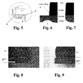
- the MMC Package Outline is a not regular polygon as it presents a 45° chamfer, as shown in Figure 3.
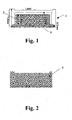
- Figure 1 shows a schematic view of a MMC package 1 according to the prior art with its main dimensions. Note that the dimensions of the substrate 2 does not make good use of the 24.0 mm width of the PCB 3, thus reducing the surface available for the electronic components.
- the moulding thickness that is 0.75 mm, is critical because the Sensor Die minimum thickness is 0.70 mm.
- the required rounded corners on the bottom of the MMC 1 are obtained according to the prior art with a proper shaping of the plastic lid.
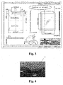
- FIG. 2 shows a schematic view of a fully moulded MMC package 5 obtained with the new technique of the present invention.
- This new technique permits to use all the 24.0 mm width of the MMC package for the substrate 2, thus increasing the surface available for electronic components.
- Figure 3 shows the MMC card dimensions specification defined by the MMC Organization. Note the 45° chamfer and the rounded corner on the MMC bottom side required by the MMC Organization, as the MMC package is not an SMD package, but people must handle safely these devices.
- the new substrate design provides for defining a rounded groove 4 on the substrate back side 8 all around the MMC profile, as shown in Figure 4.
- This groove has been obtained by partial laser incision or by mechanical milling cutter, using standard process already in use.
- the groove has a partial circular shape and, more specifically looks like a half period of a sinusoidal wave.
- Figure 4 shows a picture obtained with a microscope of said rounded groove on the back side of the substrate 2.
- the size of the groove 4 in comparison with the substrate thickness is shown in the schematic enlarged scale view of figure 5.
- Figure 6 shows the execution of the laser cutting technique for the fully moulded MMC package of the present invention.
- Figures 8 and 9 show a comparison between the edges of the fully moulded MMC package obtained with the laser-cutting technique of the invention (left) and the edges of a standard MMC package obtained with a standard technique.
- a laser cutting line 9 passes at one side of the peak recess 7 formed by the groove 4.
- the laser cutting line 9 is provided very close to the point in which the curved profile of the groove 4 tends to reach a 45° slope.
- the cutting point may vary according to the physical shape of the groove, but in a range of value wherein the slope of a line tangent to the grove profile is between 35° and 55°, if compared to a 0° line passing from the point of the peak recess 7.
Landscapes
- Engineering & Computer Science (AREA)
- Physics & Mathematics (AREA)
- General Physics & Mathematics (AREA)
- Theoretical Computer Science (AREA)
- Computer Hardware Design (AREA)
- Microelectronics & Electronic Packaging (AREA)
- Encapsulation Of And Coatings For Semiconductor Or Solid State Devices (AREA)
- Laser Beam Processing (AREA)
- Structures Or Materials For Encapsulating Or Coating Semiconductor Devices Or Solid State Devices (AREA)
Abstract
- providing a rounded groove (4) on a substrate (2) back side (8) of the package, all around the package profile;
- cutting the edges of said package (5) by a laser cutting line (9) passing through said groove (4).
Description
- The present invention relates to a method for manufacturing a fully moulded Multi Media Card package obtained by laser cutting.
- The invention described hereafter refers to a new technique for manufacturing of the Multi Media Card (MMC). This invention is a new method for MMC singulation including at least a cutting phase with laser cutting.
- A Multi Media Card (MMC) is a product born as memory extension in applications such as: Digital Cameras, Pocket PCs, Hand phones etc... This product includes a certain number of components assembled in a package defined by a MMC Organization.
- The MMC may not be considered a Surface Mounted Device (SMD), even if it's realised on a semiconductor substrate and includes a certain number of electronic components, on the contrary it is a card that the final user can handle and can insert and remove from a dedicated slot in cellular phones, digital cameras, pocket PCs and similar portable devices.
- For this reason a particular outline of the product has been defined by the MMC Organization and this outline does not allow the use of the standard assembly process used for SMD.
- The most advanced packaging technology for MMC production foresees that after a moulding process, similar to the one used for obtaining a SMD and in which the separation (or singulation) of each single package is done by mechanical punching before lid attachment, the final packaging will be done using an extra plastic lid that is bonded with glue on the substrate and on the mould.
- In this way a package that has a specific MMC profile, as required by MMC Media Card, has been obtained. In particular the required rounded corners on the bottom of the MMC are obtained with a proper shaping of the plastic lid.
- Even though this advanced packaging technology allows the use of a SMD production line for the MMC production, there are some difficulties in the singulation and finishing operations.
- Moreover the moulding thickness, that is 0.75 mm, is critical because the Sensor Die minimum thickness is 0.70 mm.
- In order to increase the moulding thickness and the surface usable for components on the Printed Circuit Board (PCB), it could be useful to increase the PCB width up to 24.0 mm, making good use of all the width of the MMC.
- Nevertheless, as the MMC package outline is not a regular polygon (see the chamfer at 45 degree at one side) the standard blade process, used for singulation of SMD, cannot be applied to the MMC substrate with sufficient efficiency.
- In the last years a lot of improvement has been obtained in the laser cut process for organic materials, such as the material used for PCB as substrate for MMC. The laser cutting can be a very interesting solution for singulation of MMC especially as the profile is not square or rectangular.
- However, new PCB design requires that the substrate presents rounded corners on its bottom, but the standard laser cutting technique does not guarantee this particular shape of the substrate.
- The aim of the present invention is that of providing a new manufacturing technique for obtaining Multi Media Cards by at least a laser cutting phase and with a final MMC package including rounded edges or corners.
- The invention here disclosed suggests to adopt a special substrate design and a new singulation process that allow to obtain the particular shape of the MMC.
- In particular, the new substrate design foresees a rounded groove on the substrate back side, all around the MMC profile, obtained by partial laser incision or mechanical milling cutter. This groove permits the use of standard laser cutting process for MMC singulation, obtaining the required MMC profile, and in particular the rounded corner on the bottom side of the MMC.
- Moreover, this new technique permits to use all the 24.0 mm width of MMC for the substrate increasing the surface available for electronic components. The MMC obtained with this new scenario are called Full Moulded MMC.
- According to the above solution idea, the invention related to a method defined in the annexed
claim 1. - Moreover, the invention relates to a fully moulded Multi Media Card package obtained with the above method.
- The features and advantages of the method and the package according to the invention will be disclosed hereinafter by way of a non limiting example given as a best mode of realisation with reference to enclosed drawings.
-
- Figure 1 shows a pictorial view of a MMC already in production with an indication of the main dimensions;
- Figure 2 shows a pictorial view of the Full moulded MMC obtained with a new technique according to the invention;
- Figure 3 shows a MMC card dimensions specification defined by the MMC Organization;
- Figure 4 shows a picture obtained with a microscope of the rounded groove on the back side of the substrate all around the MMC profile;
- Figure 5 shows an enlarged scale particular of a said rounded groove of figure 4 obtained on the back side of the substrate all around the MMC package profile;
- Figure 6 shows a picture obtained with a microscope of the above rounded groove before a laser cutting phase;
- Figure 7 shows a picture obtained with a microscope after the execution of the laser cutting technique for the Full Moulded MMC package according to the present invention;
- Figures 8 and 9 show a picture comparison between the Full Moulded MMC edges obtained with the laser-cutting new technique (left) and standard MMC edges obtained with the standard technique, respectively.
- In order to achieve a fully moulded MMC structure, using the same moulding process used in Plastic Ball Grid Array (PBGA) and then to obtain MMC package in complete agreement with MMC specification requirements, a new substrate design and a new laser cutting technique for package "singulation" is proposed hereinafter.
- In fact, laser process has the advantage that MMC can be singulated sawing only the substrate and following the package profile with big accuracy, position by position.
- The main requirement that distinguishes the MMC from the standard SMD packages is that people shall handle safely the MMC package. For this reason, at least some of corners all around the package and at least some of the edges have to be not sharp but with sufficient smoothness, as shown in Figure 3.
- Moreover, the MMC Package Outline is a not regular polygon as it presents a 45° chamfer, as shown in Figure 3.
- The two requirements here above described impede the application of both the standard blade process and the standard laser cutting technique to the production of MMC.
- Figure 1 shows a schematic view of a
MMC package 1 according to the prior art with its main dimensions. Note that the dimensions of thesubstrate 2 does not make good use of the 24.0 mm width of thePCB 3, thus reducing the surface available for the electronic components. - Moreover the moulding thickness, that is 0.75 mm, is critical because the Sensor Die minimum thickness is 0.70 mm. In this configuration, the required rounded corners on the bottom of the
MMC 1 are obtained according to the prior art with a proper shaping of the plastic lid. - Figure 2 shows a schematic view of a fully moulded
MMC package 5 obtained with the new technique of the present invention. This new technique permits to use all the 24.0 mm width of the MMC package for thesubstrate 2, thus increasing the surface available for electronic components. - Figure 3 shows the MMC card dimensions specification defined by the MMC Organization. Note the 45° chamfer and the rounded corner on the MMC bottom side required by the MMC Organization, as the MMC package is not an SMD package, but people must handle safely these devices.
- In order to apply the standard laser-cutting technique to the manufacturing process of the Full Moulded MMC, a special substrate design and a new singulation process are proposed.
- The new substrate design provides for defining a
rounded groove 4 on the substrate back side 8 all around the MMC profile, as shown in Figure 4. - This groove has been obtained by partial laser incision or by mechanical milling cutter, using standard process already in use.
- The groove has a partial circular shape and, more specifically looks like a half period of a sinusoidal wave.
- Figure 4 shows a picture obtained with a microscope of said rounded groove on the back side of the
substrate 2. - The size of the
groove 4 in comparison with the substrate thickness is shown in the schematic enlarged scale view of figure 5. - After the
groove 4 definition, a solder mask already used for the organic substrate is deposed and uniformed inside the groove. - With this substrate definition it is possible to cut the substrate with laser (the laser beam is 0,1 mm wide) from the top side, just in correspondence of the
groove 4 on the back side, as shown in Figure 6. - Figure 6 shows the execution of the laser cutting technique for the fully moulded MMC package of the present invention.
- In this way, it is possible to obtain the profile required for MMC by the MMC Organization.
- The results obtained on the Full Moulded MMC manufactured and singulated with this new substrate definition and laser-cutting process are very interesting. As shown in Figures 8 and 9, this new technique allows to obtain very smooth edges.
- Figures 8 and 9 show a comparison between the edges of the fully moulded MMC package obtained with the laser-cutting technique of the invention (left) and the edges of a standard MMC package obtained with a standard technique.
- As may be appreciated from the example of figure 6, a
laser cutting line 9 passes at one side of thepeak recess 7 formed by thegroove 4. - In other words, the
laser cutting line 9 is provided very close to the point in which the curved profile of thegroove 4 tends to reach a 45° slope. - The cutting point may vary according to the physical shape of the groove, but in a range of value wherein the slope of a line tangent to the grove profile is between 35° and 55°, if compared to a 0° line passing from the point of the
peak recess 7. - In conclusion, the advantages of this new technology, called Full Moulded MMC, are listed hereafter:
- Cost saving;
- Package outline according the MMC Organization standards, and characterised by:
- Usable area at least 50% bigger than in the capped version;
- Thickness of moulded cap 1.05 mm instead of 0.75 mm in the capped version (see Figure 2);
- Simpler assembly process;
- Better reliability.
- In view of the above description, it will be appreciated that, although specific embodiments of the invention have been described herein for purposes of illustration, various modifications may be made without deviating from the spirit and scope of the invention. Accordingly, the invention is not limited except as by the appended claims.
Claims (6)
- A method for manufacturing a fully moulded Multi Media Card package (5) obtained by laser cutting wherein at least some edges and the corners around the package have rounded profile and a sufficient smoothness for a safe handling, characterised by:- providing a rounded groove (4) on a substrate (2) back side (8) of the package, all around the package profile;- cutting the edges of said package (5) by a laser cutting line (9) passing through said groove (4).
- A method according to claim 1, wherein said groove is obtained by partial laser incision or by mechanical milling cutter.
- A method according to claim 1, wherein said laser cutting line (9) passes at one side of a peak recess (7) formed by the said groove (4).
- A method according to claim 3, wherein said laser cutting line (9) passes close to the point in which the curved profile of the groove (4) tends to reach a 45° slope.
- A method according to claim 1, wherein the shape of said groove is similar to a half a period of a sinusoidal wave.
- A fully moulded Multi Media Card package (5) obtained by laser cutting wherein at least some edges and the corners around the package have rounded profile and a sufficient smoothness for a safe handling, characterised by:- said rounded edges are obtained providing a rounded groove (4) on a substrate (2) back side (8) of the package, all around the package profile;- cutting the edges of said package (5) by a laser cutting line (9) passing through said groove (4), according to one of the previous claims.
Priority Applications (3)
| Application Number | Priority Date | Filing Date | Title |
|---|---|---|---|
| DE602004010905T DE602004010905D1 (en) | 2004-08-31 | 2004-08-31 | Method for producing an MMC multimedia card by means of injection molding and laser cutting methods |
| EP04425646A EP1630729B1 (en) | 2004-08-31 | 2004-08-31 | A method for manufacturing a moulded MMC multi media card package obtained with laser cutting |
| US11/218,309 US7803663B2 (en) | 2004-08-31 | 2005-08-31 | Method for manufacturing a molded MMC multi media card package obtained with laser cutting |
Applications Claiming Priority (1)
| Application Number | Priority Date | Filing Date | Title |
|---|---|---|---|
| EP04425646A EP1630729B1 (en) | 2004-08-31 | 2004-08-31 | A method for manufacturing a moulded MMC multi media card package obtained with laser cutting |
Publications (2)
| Publication Number | Publication Date |
|---|---|
| EP1630729A1 true EP1630729A1 (en) | 2006-03-01 |
| EP1630729B1 EP1630729B1 (en) | 2007-12-26 |
Family
ID=34932734
Family Applications (1)
| Application Number | Title | Priority Date | Filing Date |
|---|---|---|---|
| EP04425646A Expired - Lifetime EP1630729B1 (en) | 2004-08-31 | 2004-08-31 | A method for manufacturing a moulded MMC multi media card package obtained with laser cutting |
Country Status (3)
| Country | Link |
|---|---|
| US (1) | US7803663B2 (en) |
| EP (1) | EP1630729B1 (en) |
| DE (1) | DE602004010905D1 (en) |
Families Citing this family (2)
| Publication number | Priority date | Publication date | Assignee | Title |
|---|---|---|---|---|
| JP6698661B2 (en) * | 2014-12-29 | 2020-05-27 | エレクトロ サイエンティフィック インダストリーズ インコーポレーテッド | Adaptive partial profile generation via independent lateral measurement using alignment features |
| DE102015110429A1 (en) * | 2015-06-29 | 2017-01-12 | Osram Opto Semiconductors Gmbh | Optoelectronic lighting device |
Citations (3)
| Publication number | Priority date | Publication date | Assignee | Title |
|---|---|---|---|---|
| JPH01292638A (en) * | 1988-05-20 | 1989-11-24 | Fuji Photo Film Co Ltd | Card and its production |
| JP2001076105A (en) * | 1999-09-08 | 2001-03-23 | Toppan Printing Co Ltd | Plug-in IC card and method for producing the same |
| DE10252351A1 (en) * | 2002-11-11 | 2004-05-19 | Giesecke & Devrient Gmbh | Minichip card manufacturing method in which the minichip card within its card body passes through the production process including initialization and customization before being divided from the card body using laser cutting |
Family Cites Families (5)
| Publication number | Priority date | Publication date | Assignee | Title |
|---|---|---|---|---|
| DE2551323A1 (en) * | 1974-11-19 | 1976-05-20 | Battelle Memorial Institute | METHOD OF FORMING THE MESH FOR A KNITTED KNITTING AND KNITTING DEVICE FOR CARRYING OUT THE METHOD |
| US5128282A (en) * | 1991-11-04 | 1992-07-07 | Xerox Corporation | Process for separating image sensor dies and the like from a wafer that minimizes silicon waste |
| US5908247A (en) * | 1994-11-14 | 1999-06-01 | Seagate Technology, Inc. | Sinusoidal grooving pattern for grooved journal bearing |
| JP2005523583A (en) * | 2002-04-19 | 2005-08-04 | エグシル テクノロジー リミテッド | Programmed dicing of substrates using pulsed laser |
| US7129114B2 (en) * | 2004-03-10 | 2006-10-31 | Micron Technology, Inc. | Methods relating to singulating semiconductor wafers and wafer scale assemblies |
-
2004
- 2004-08-31 DE DE602004010905T patent/DE602004010905D1/en not_active Expired - Lifetime
- 2004-08-31 EP EP04425646A patent/EP1630729B1/en not_active Expired - Lifetime
-
2005
- 2005-08-31 US US11/218,309 patent/US7803663B2/en active Active
Patent Citations (3)
| Publication number | Priority date | Publication date | Assignee | Title |
|---|---|---|---|---|
| JPH01292638A (en) * | 1988-05-20 | 1989-11-24 | Fuji Photo Film Co Ltd | Card and its production |
| JP2001076105A (en) * | 1999-09-08 | 2001-03-23 | Toppan Printing Co Ltd | Plug-in IC card and method for producing the same |
| DE10252351A1 (en) * | 2002-11-11 | 2004-05-19 | Giesecke & Devrient Gmbh | Minichip card manufacturing method in which the minichip card within its card body passes through the production process including initialization and customization before being divided from the card body using laser cutting |
Non-Patent Citations (2)
| Title |
|---|
| PATENT ABSTRACTS OF JAPAN vol. 014, no. 078 (P - 1006) 14 February 1990 (1990-02-14) * |
| PATENT ABSTRACTS OF JAPAN vol. 2000, no. 20 10 July 2001 (2001-07-10) * |
Also Published As
| Publication number | Publication date |
|---|---|
| EP1630729B1 (en) | 2007-12-26 |
| US20060057823A1 (en) | 2006-03-16 |
| US7803663B2 (en) | 2010-09-28 |
| DE602004010905D1 (en) | 2008-02-07 |
Similar Documents
| Publication | Publication Date | Title |
|---|---|---|
| US7488620B2 (en) | Method of fabricating leadframe based flash memory cards including singulation by straight line cuts | |
| JP5117048B2 (en) | Method for efficiently manufacturing a removable peripheral card | |
| US7253027B2 (en) | Method of manufacturing hybrid integrated circuit device | |
| JP2010278309A (en) | Circuit board manufacturing method and circuit device manufacturing method | |
| EP1630729B1 (en) | A method for manufacturing a moulded MMC multi media card package obtained with laser cutting | |
| EP3340377B1 (en) | Creating antennas connected to printed chips by post processing with a laser or other cutting device | |
| CN105008105B (en) | Mould, the method with encapsulation electronic component, the carrier of the encapsulation electronic component of separation and for encapsulating electronic component | |
| JP2002016189A (en) | IC package and method of manufacturing IC package | |
| US20090121361A1 (en) | Semiconductor device and method for manufacturing thereof | |
| JP2002092575A (en) | Small card and its manufacturing method | |
| EP2674897B1 (en) | A data carrier having a microcircuit card and a method for making such a card | |
| JP2010080651A (en) | Method of manufacturing semiconductor device | |
| KR100576421B1 (en) | Sing-punch punch used for singulation process of BA package | |
| CN111048318A (en) | Valve metal foil and method for manufacturing same | |
| TWI343096B (en) | Method for forming a memory card | |
| CN101008988A (en) | Encapsulation method and structure of flash memory card | |
| JP2003340791A (en) | Method for slitting heterogeneous laminate material | |
| JP2002236895A (en) | IC carrier with plate frame | |
| EP1615165A1 (en) | Chip card with prevention of crack propagation in the card body | |
| CN101008989A (en) | Encapsulation method and structure of flash memory card | |
| JP2000033594A (en) | Cutting method for sheet member | |
| CN107749747A (en) | A kind of ceramic block array, ceramic block and the preparation method of ceramic block | |
| KR19990000254A (en) | Board connection and unification method to reduce materials | |
| KR20120059791A (en) | Dicing blade | |
| TWM312752U (en) | Package structure of flash memory card |
Legal Events
| Date | Code | Title | Description |
|---|---|---|---|
| PUAI | Public reference made under article 153(3) epc to a published international application that has entered the european phase |
Free format text: ORIGINAL CODE: 0009012 |
|
| AK | Designated contracting states |
Kind code of ref document: A1 Designated state(s): AT BE BG CH CY CZ DE DK EE ES FI FR GB GR HU IE IT LI LU MC NL PL PT RO SE SI SK TR |
|
| AX | Request for extension of the european patent |
Extension state: AL HR LT LV MK |
|
| AKX | Designation fees paid | ||
| 17P | Request for examination filed |
Effective date: 20060830 |
|
| RBV | Designated contracting states (corrected) |
Designated state(s): DE FR GB IT |
|
| REG | Reference to a national code |
Ref country code: DE Ref legal event code: 8566 |
|
| 17Q | First examination report despatched |
Effective date: 20061128 |
|
| GRAP | Despatch of communication of intention to grant a patent |
Free format text: ORIGINAL CODE: EPIDOSNIGR1 |
|
| GRAS | Grant fee paid |
Free format text: ORIGINAL CODE: EPIDOSNIGR3 |
|
| GRAA | (expected) grant |
Free format text: ORIGINAL CODE: 0009210 |
|
| AK | Designated contracting states |
Kind code of ref document: B1 Designated state(s): DE FR GB IT |
|
| REG | Reference to a national code |
Ref country code: GB Ref legal event code: FG4D |
|
| REF | Corresponds to: |
Ref document number: 602004010905 Country of ref document: DE Date of ref document: 20080207 Kind code of ref document: P |
|
| EN | Fr: translation not filed | ||
| PG25 | Lapsed in a contracting state [announced via postgrant information from national office to epo] |
Ref country code: DE Free format text: LAPSE BECAUSE OF FAILURE TO SUBMIT A TRANSLATION OF THE DESCRIPTION OR TO PAY THE FEE WITHIN THE PRESCRIBED TIME-LIMIT Effective date: 20080327 |
|
| PLBE | No opposition filed within time limit |
Free format text: ORIGINAL CODE: 0009261 |
|
| STAA | Information on the status of an ep patent application or granted ep patent |
Free format text: STATUS: NO OPPOSITION FILED WITHIN TIME LIMIT |
|
| 26N | No opposition filed |
Effective date: 20080929 |
|
| PG25 | Lapsed in a contracting state [announced via postgrant information from national office to epo] |
Ref country code: FR Free format text: LAPSE BECAUSE OF FAILURE TO SUBMIT A TRANSLATION OF THE DESCRIPTION OR TO PAY THE FEE WITHIN THE PRESCRIBED TIME-LIMIT Effective date: 20081017 |
|
| PGFP | Annual fee paid to national office [announced via postgrant information from national office to epo] |
Ref country code: GB Payment date: 20110728 Year of fee payment: 8 |
|
| PGFP | Annual fee paid to national office [announced via postgrant information from national office to epo] |
Ref country code: IT Payment date: 20110723 Year of fee payment: 8 |
|
| GBPC | Gb: european patent ceased through non-payment of renewal fee |
Effective date: 20120831 |
|
| PG25 | Lapsed in a contracting state [announced via postgrant information from national office to epo] |
Ref country code: IT Free format text: LAPSE BECAUSE OF NON-PAYMENT OF DUE FEES Effective date: 20120831 |
|
| PG25 | Lapsed in a contracting state [announced via postgrant information from national office to epo] |
Ref country code: GB Free format text: LAPSE BECAUSE OF NON-PAYMENT OF DUE FEES Effective date: 20120831 |