EP1627718A1 - Method of decorating surface of mold and mold - Google Patents
Method of decorating surface of mold and mold Download PDFInfo
- Publication number
- EP1627718A1 EP1627718A1 EP04734420A EP04734420A EP1627718A1 EP 1627718 A1 EP1627718 A1 EP 1627718A1 EP 04734420 A EP04734420 A EP 04734420A EP 04734420 A EP04734420 A EP 04734420A EP 1627718 A1 EP1627718 A1 EP 1627718A1
- Authority
- EP
- European Patent Office
- Prior art keywords
- die
- photomask
- pattern
- photoresist
- molding
- Prior art date
- Legal status (The legal status is an assumption and is not a legal conclusion. Google has not performed a legal analysis and makes no representation as to the accuracy of the status listed.)
- Withdrawn
Links
Images


Classifications
-
- G—PHYSICS
- G03—PHOTOGRAPHY; CINEMATOGRAPHY; ANALOGOUS TECHNIQUES USING WAVES OTHER THAN OPTICAL WAVES; ELECTROGRAPHY; HOLOGRAPHY
- G03F—PHOTOMECHANICAL PRODUCTION OF TEXTURED OR PATTERNED SURFACES, e.g. FOR PRINTING, FOR PROCESSING OF SEMICONDUCTOR DEVICES; MATERIALS THEREFOR; ORIGINALS THEREFOR; APPARATUS SPECIALLY ADAPTED THEREFOR
- G03F7/00—Photomechanical, e.g. photolithographic, production of textured or patterned surfaces, e.g. printing surfaces; Materials therefor, e.g. comprising photoresists; Apparatus specially adapted therefor
- G03F7/20—Exposure; Apparatus therefor
- G03F7/24—Curved surfaces
-
- B—PERFORMING OPERATIONS; TRANSPORTING
- B29—WORKING OF PLASTICS; WORKING OF SUBSTANCES IN A PLASTIC STATE IN GENERAL
- B29C—SHAPING OR JOINING OF PLASTICS; SHAPING OF MATERIAL IN A PLASTIC STATE, NOT OTHERWISE PROVIDED FOR; AFTER-TREATMENT OF THE SHAPED PRODUCTS, e.g. REPAIRING
- B29C33/00—Moulds or cores; Details thereof or accessories therefor
- B29C33/38—Moulds or cores; Details thereof or accessories therefor characterised by the material or the manufacturing process
-
- B—PERFORMING OPERATIONS; TRANSPORTING
- B29—WORKING OF PLASTICS; WORKING OF SUBSTANCES IN A PLASTIC STATE IN GENERAL
- B29C—SHAPING OR JOINING OF PLASTICS; SHAPING OF MATERIAL IN A PLASTIC STATE, NOT OTHERWISE PROVIDED FOR; AFTER-TREATMENT OF THE SHAPED PRODUCTS, e.g. REPAIRING
- B29C33/00—Moulds or cores; Details thereof or accessories therefor
- B29C33/56—Coatings, e.g. enameled or galvanised; Releasing, lubricating or separating agents
-
- G—PHYSICS
- G03—PHOTOGRAPHY; CINEMATOGRAPHY; ANALOGOUS TECHNIQUES USING WAVES OTHER THAN OPTICAL WAVES; ELECTROGRAPHY; HOLOGRAPHY
- G03F—PHOTOMECHANICAL PRODUCTION OF TEXTURED OR PATTERNED SURFACES, e.g. FOR PRINTING, FOR PROCESSING OF SEMICONDUCTOR DEVICES; MATERIALS THEREFOR; ORIGINALS THEREFOR; APPARATUS SPECIALLY ADAPTED THEREFOR
- G03F1/00—Originals for photomechanical production of textured or patterned surfaces, e.g., masks, photo-masks, reticles; Mask blanks or pellicles therefor; Containers specially adapted therefor; Preparation thereof
- G03F1/60—Substrates
-
- G—PHYSICS
- G03—PHOTOGRAPHY; CINEMATOGRAPHY; ANALOGOUS TECHNIQUES USING WAVES OTHER THAN OPTICAL WAVES; ELECTROGRAPHY; HOLOGRAPHY
- G03F—PHOTOMECHANICAL PRODUCTION OF TEXTURED OR PATTERNED SURFACES, e.g. FOR PRINTING, FOR PROCESSING OF SEMICONDUCTOR DEVICES; MATERIALS THEREFOR; ORIGINALS THEREFOR; APPARATUS SPECIALLY ADAPTED THEREFOR
- G03F1/00—Originals for photomechanical production of textured or patterned surfaces, e.g., masks, photo-masks, reticles; Mask blanks or pellicles therefor; Containers specially adapted therefor; Preparation thereof
- G03F1/68—Preparation processes not covered by groups G03F1/20 - G03F1/50
- G03F1/76—Patterning of masks by imaging
-
- G—PHYSICS
- G03—PHOTOGRAPHY; CINEMATOGRAPHY; ANALOGOUS TECHNIQUES USING WAVES OTHER THAN OPTICAL WAVES; ELECTROGRAPHY; HOLOGRAPHY
- G03F—PHOTOMECHANICAL PRODUCTION OF TEXTURED OR PATTERNED SURFACES, e.g. FOR PRINTING, FOR PROCESSING OF SEMICONDUCTOR DEVICES; MATERIALS THEREFOR; ORIGINALS THEREFOR; APPARATUS SPECIALLY ADAPTED THEREFOR
- G03F7/00—Photomechanical, e.g. photolithographic, production of textured or patterned surfaces, e.g. printing surfaces; Materials therefor, e.g. comprising photoresists; Apparatus specially adapted therefor
- G03F7/26—Processing photosensitive materials; Apparatus therefor
- G03F7/40—Treatment after imagewise removal, e.g. baking
Definitions
- the present invention relates to a die used for resin molding such as injection molding, and a method for decorating the surface of the die.
- resin molding that is molded by injection molding or the like can have a variety of facades depending on die surface decorations.
- die surface decorations in molding there has been known an etching method by which to corrode the die through the functions of chemical agents, making it possible to form on the die surface a variety of patterns such as satin finished surface, leathery surface, grain woody texture, linear embossing, geometric patterns or the like.
- a sand-blast (honing) processing that forms a fine pattern on the surface of an object by physically blasting and glass beads.
- photomasks 11, 12, and 13 are made by cutting off a photoengraved film-like photomask according to a plan view spread out based on the shape of a die. Then, as shown in FIG. 3B, the cut-off photomasks 11, 12, and 13 are stuck to a die 20 coated with a photoresist, and seams of the photomasks are joined together by tapes or the like to be exposed and developed. Next, the developed condition of the photoresist is examined, and after discontinuity in the joined parts of the photomasks is corrected, etching is performed to form a pattern on the die 20.
- the masking method that uses photoresist has a high feasibility of molding a pattern with high accuracy when it is compared with the above-mentioned masking method.
- the photomask must be cut apart and then joined with each other on a three-dimensional die, which leads to an occurrence somewhere of a seam between the photoresist, making perfect transcription impossible.
- FIG. 3C there remains a seam 20a in the pattern on the surface of the die, which is a problem in terms of exterior appearance.
- a second invention is a method for decorating the surface of a die according to the first invention, wherein molding the film-like photomask into the same shape as that of aforesaid die is performed by sticking a heated photomask to a predetermined die.
- a third invention is a die for resin molding wherein a film-like photomask molded into the same shape as that of aforesaid die is stuck to a photoresist coated on the surface of aforesaid die to be exposed and developed for etching, and a pattern made on aforesaid photomask is formed on the surface thereof.
- a first invention is a method for decorating the surface of a die which comprises the steps of coating the surface of the die with a photoresist; molding a film-like photomask into the same shape as that of aforesaid die; sticking the photomask molded into aforesaid shape to aforesaid die coated with the photoresist to be exposed and developed; and etching a pattern formed on aforesaid photomask into aforesaid developed die.
- a pattern can be uniformly formed without difficulties on the surface of a die having a three-dimensional curved surface and molded components with an excellent appearance can be obtained. Accordingly, a wide range of three-dimensional designs as has been conventionally impossible can be obtained, enabling value-added products to be provided.
- FIG. 1 is a perspective view showing an example of the shape of a die to which this embodiment is applied.
- a die 1 is one for molding a diaphragm used in a speaker.
- the die 1 has a cone-shaped three-dimensionally curved surface part la, and in this embodiment, on account of design and the like, a pattern such as a geometric pattern and the like will be formed on the overall surface of the diaphragm including the cone-shaped three-dimensional curved surface part 1a.
- FIGS. 2A to 2H show an example of an operational process for decorating the surface of a die according to the embodiment of the present invention.
- a photomask 2 shown in FIG. 2A is made.
- the design to be formed is a grid-like pattern.
- This pattern is drawn by a CAD (Computer Aided Design) and photoengraved on a polyester film of 100 ⁇ m in thickness. This is the photomask 2 in which forming of a pattern is finished.
- CAD Computer Aided Design
- the photomask 2 is heated using a far-infrared ray heater 3 in order to be molded into the same shape as that of a die.
- Temperature and heating time in this case are respectively selected in the range of 170°C to 180°C of not destroying the molded pattern and 20sec to 30sec. Since the temperature and time depend on the thickness of the film that is used as the photomask 2, conditions are not restricted to the above described ones.
- the heated photomask 2 is stuck to a molding die 4 by means of a vacuum molding method and is molded.
- the photomask 2' molded into the same shape as that of the die is stuck to a dried die 1' coated with a photoresist, which is exposed to predetermined energy and spray-developed with 1% sodium carbonate aqueous solution of 20°C in temperature, for example.
- a seamless pattern can be transcribed onto the die 1' .
- procedures can be simplified.
- the above pattern-transcribed die 1' is sprayed with iron chloride aqueous solution, and after rinsed in water, the photoresist is exfoliated by, for example, 2% sodium hydroxide aqueous solution of 50 °C in temperature to provide an etching-finished die 1" with a predetermined pattern formed thereon, as shown in FIG. 2H.
- the molded diaphragm When a diaphragm is injection-molded using the die 1" formed by the process as described above, the molded diaphragm has a uniform pattern formed on the whole surface including the cone shape thereof to have an excellent external appearance. That is, a seam 20a shown in FIG. 3C as a conventional example does not remain on the surface, with the result that a pattern drawn in the photomask 2 is formed on a molded component exactly as it is.
- a film used as the photomask according to this embodiment is formed of a general-purpose polyester film coated with a photo-sensitive material and the thickness thereof is preferably 100 ⁇ m or more and 250 ⁇ m or less, and the film is required to be capable of being molded by such molding technology as vacuum molding or the like. Needless to say, other materials and thickness than those of the above described film can be used as long as they have the feasibility of vacuum molding.
- a photosensitive material coated thereon is not particularly specified; however the material preferably possesses thermal resistance, so that when a pattern-formed film is vacuum-molded, the material extends accordingly to the amount of stretch of a base polyester without destroying the formed pattern due to heat at the time of molding.
- photoresist used in this embodiment may be either of a negative type or a positive type as long as the photoresist has the feasibility of being spray-coated because it needs to be coated on a three-dimensionally curved surface, and becomes tack-free when dried.
- a light source that is used at a time of the exposure of the photoresist is preferably a device that can more or less change an angle of light thereof, because the amount of exposure of the vertical surface of a die with respect to the direction of the light source is not sufficient; and the light source is not specifically limited as long as it is corresponding to an absorption wavelength of the photoresist.
- the present invention is applied to the die for molding the diaphragm used in a speaker, needless to say the above described embodiment can be applied to a die for molding other resin components.
- a pattern to be formed on the surface of a die a letter or symbol, not a uniform pattern mentioned above, may be formed on the surface thereof as a pattern.
- a pattern can be uniformly formed without difficulties on the surface of a die having a three-dimensional curved surface and molded components with an excellent appearance can be obtained. Accordingly, a wide range of three-dimensional designs as has been conventionally impossible can be obtained, enabling value-added products to be provided.
Landscapes
- Physics & Mathematics (AREA)
- General Physics & Mathematics (AREA)
- Engineering & Computer Science (AREA)
- Mechanical Engineering (AREA)
- Manufacturing & Machinery (AREA)
- Moulds For Moulding Plastics Or The Like (AREA)
- Shaping Of Tube Ends By Bending Or Straightening (AREA)
- Preparing Plates And Mask In Photomechanical Process (AREA)
- Photosensitive Polymer And Photoresist Processing (AREA)
Abstract





Description
- The present invention relates to a die used for resin molding such as injection molding, and a method for decorating the surface of the die.
- Of late, the external appearance and finish of plastic molding used in automobiles and home electric appliances have come to be highly valued in order to enhance luxury as well as to increase an added-value of commercial merchandise. Particularly, resin molding that is molded by injection molding or the like can have a variety of facades depending on die surface decorations. Conventionally, of the die surface decorations in molding, there has been known an etching method by which to corrode the die through the functions of chemical agents, making it possible to form on the die surface a variety of patterns such as satin finished surface, leathery surface, grain woody texture, linear embossing, geometric patterns or the like. In addition, there is known a sand-blast (honing) processing that forms a fine pattern on the surface of an object by physically blasting and glass beads.
- On the other hand, there is known a method of exposing a metal part of the portion necessary for etching or similar by spraying a photoresist in liquid form across the whole of a die and sticking a photoengraved film-like photomask to the die to be exposed and developed.
- Hereinafter, a method using a conventional film-like photomask will be explained with reference to FIGS. 3.
- First, as shown in FIG. 3A,
photomasks photomasks die 20 coated with a photoresist, and seams of the photomasks are joined together by tapes or the like to be exposed and developed. Next, the developed condition of the photoresist is examined, and after discontinuity in the joined parts of the photomasks is corrected, etching is performed to form a pattern on thedie 20. - Meanwhile, there is known another method of directly exposing a photoresist coated on a die by using laser beams.
- In Japanese published patent application No. 51-63866 published by the Japanese Patent Office, a method is disclosed in which concavity and convexity are formed by an etching process on the core side surface of a die used for injection molding.
- However, the decorations by the etching method and sand-blast process (honing) have been rarely applied to the whole of the die, so that it is necessary to cover and hide the parts to which it is unnecessary to apply thereof by adhesive tapes for masking or the like. There are many cases where it depends on manual work such as when the die has a complicated three-dimensional configuration and when it has parts in need of fine work such that it caused a lot of trouble and there was a limit in its process.
- On the other hand, the masking method that uses photoresist has a high feasibility of molding a pattern with high accuracy when it is compared with the above-mentioned masking method. However, when it comes to the case where a pattern needs to be incised on the surface of a die, the photomask must be cut apart and then joined with each other on a three-dimensional die, which leads to an occurrence somewhere of a seam between the photoresist, making perfect transcription impossible. As a result, as shown in FIG. 3C, there remains a
seam 20a in the pattern on the surface of the die, which is a problem in terms of exterior appearance. Further, there is no other way to join the photoresist than to be dependent on manual work, which requires a lot of trouble. - A second invention is a method for decorating the surface of a die according to the first invention, wherein molding the film-like photomask into the same shape as that of aforesaid die is performed by sticking a heated photomask to a predetermined die.
- A third invention is a die for resin molding wherein a film-like photomask molded into the same shape as that of aforesaid die is stuck to a photoresist coated on the surface of aforesaid die to be exposed and developed for etching, and a pattern made on aforesaid photomask is formed on the surface thereof.
- A first invention is a method for decorating the surface of a die which comprises the steps of coating the surface of the die with a photoresist; molding a film-like photomask into the same shape as that of aforesaid die; sticking the photomask molded into aforesaid shape to aforesaid die coated with the photoresist to be exposed and developed; and etching a pattern formed on aforesaid photomask into aforesaid developed die.
- By employing such a manner, a pattern can be uniformly formed without difficulties on the surface of a die having a three-dimensional curved surface and molded components with an excellent appearance can be obtained. Accordingly, a wide range of three-dimensional designs as has been conventionally impossible can be obtained, enabling value-added products to be provided.
-
- FIG. 1 is a perspective view showing an example of the shape of a die;
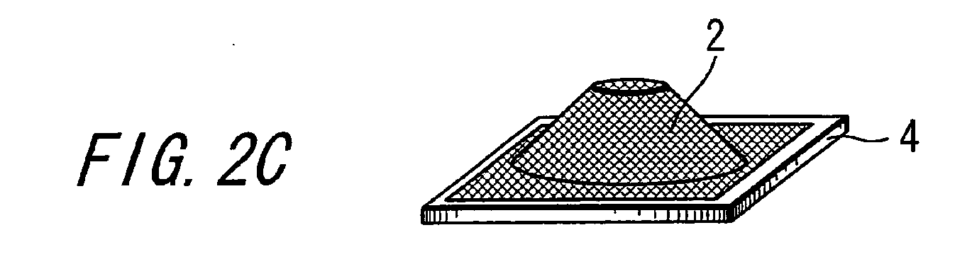
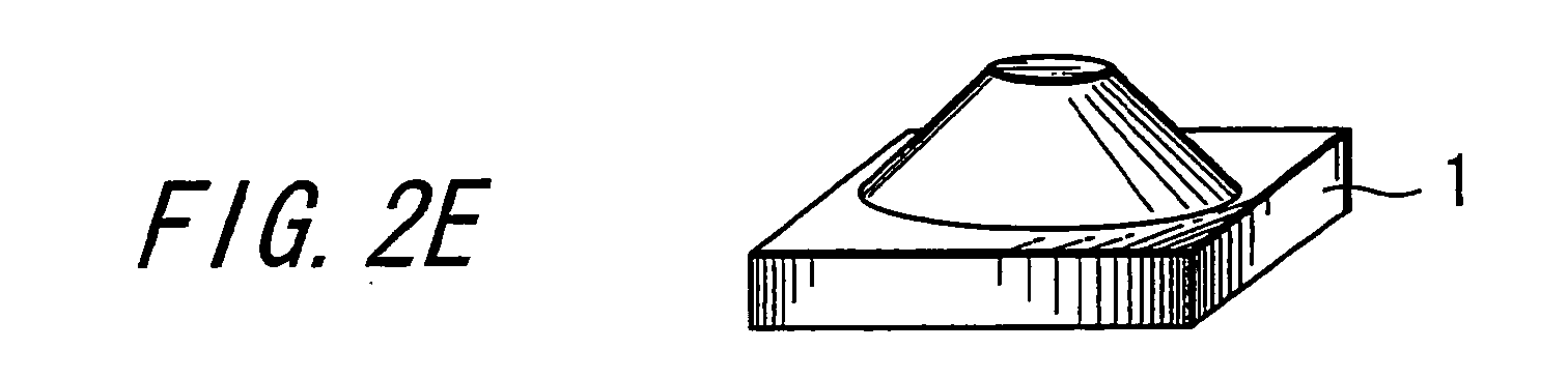
- FIG. 2A through 2H are explanatory diagrams showing a process for decorating the surface of a die according to an embodiment of the present invention; and
- FIGS. 3A to 3C are explanatory diagrams showing a process of decorating the surface of a die according to prior art.
- Hereinafter, an embodiment of the present invention will be explained with reference to FIGS. 1 and 2A to 2H.
- FIG. 1 is a perspective view showing an example of the shape of a die to which this embodiment is applied. A die 1 is one for molding a diaphragm used in a speaker. The die 1 has a cone-shaped three-dimensionally curved surface part la, and in this embodiment, on account of design and the like, a pattern such as a geometric pattern and the like will be formed on the overall surface of the diaphragm including the cone-shaped three-dimensional
curved surface part 1a. - FIGS. 2A to 2H show an example of an operational process for decorating the surface of a die according to the embodiment of the present invention.
- First, a
photomask 2 shown in FIG. 2A is made. In this embodiment, the design to be formed is a grid-like pattern. This pattern is drawn by a CAD (Computer Aided Design) and photoengraved on a polyester film of 100 µm in thickness. This is thephotomask 2 in which forming of a pattern is finished. - Next, as shown in FIG. 2B, the
photomask 2 is heated using a far-infrared ray heater 3 in order to be molded into the same shape as that of a die. Temperature and heating time in this case are respectively selected in the range of 170°C to 180°C of not destroying the molded pattern and 20sec to 30sec. Since the temperature and time depend on the thickness of the film that is used as thephotomask 2, conditions are not restricted to the above described ones. - Next, as shown in FIG. 2C, in order to mold the
heated photomask 2 into the same shape as that of thedie 1, the heated photomask is stuck to amolding die 4 by means of a vacuum molding method and is molded. - With the above described method, as shown in FIG. 2D, a photomask 2' having the same shape as that of the die is made.
- Next, of the die 1 shown in FIG. 2E, parts that are irrelevant to the process such as a part into which a mold base is inserted and the like are processed with masking tapes and the like, and then the
die 1 is subjected to a degreasing processing, dried, and spray-coated with a photoresist in liquid form; and is dried at 80°C in temperature for 15 minutes. It is shown in FIG. 2F. - Next, as shown in FIG. 2G, the photomask 2' molded into the same shape as that of the die is stuck to a dried die 1' coated with a photoresist, which is exposed to predetermined energy and spray-developed with 1% sodium carbonate aqueous solution of 20°C in temperature, for example. As a result, a seamless pattern can be transcribed onto the die 1' . In addition, since a process of correcting seams between the joined photoresists is not required, procedures can be simplified.
- The above pattern-transcribed die 1' is sprayed with iron chloride aqueous solution, and after rinsed in water, the photoresist is exfoliated by, for example, 2% sodium hydroxide aqueous solution of 50 °C in temperature to provide an etching-finished die 1" with a predetermined pattern formed thereon, as shown in FIG. 2H.
- When a diaphragm is injection-molded using the
die 1" formed by the process as described above, the molded diaphragm has a uniform pattern formed on the whole surface including the cone shape thereof to have an excellent external appearance. That is, aseam 20a shown in FIG. 3C as a conventional example does not remain on the surface, with the result that a pattern drawn in thephotomask 2 is formed on a molded component exactly as it is. - It should be noted that a film used as the photomask according to this embodiment is formed of a general-purpose polyester film coated with a photo-sensitive material and the thickness thereof is preferably 100 µm or more and 250 µm or less, and the film is required to be capable of being molded by such molding technology as vacuum molding or the like. Needless to say, other materials and thickness than those of the above described film can be used as long as they have the feasibility of vacuum molding. A photosensitive material coated thereon is not particularly specified; however the material preferably possesses thermal resistance, so that when a pattern-formed film is vacuum-molded, the material extends accordingly to the amount of stretch of a base polyester without destroying the formed pattern due to heat at the time of molding.
- Further, photoresist used in this embodiment may be either of a negative type or a positive type as long as the photoresist has the feasibility of being spray-coated because it needs to be coated on a three-dimensionally curved surface, and becomes tack-free when dried.
- A light source that is used at a time of the exposure of the photoresist is preferably a device that can more or less change an angle of light thereof, because the amount of exposure of the vertical surface of a die with respect to the direction of the light source is not sufficient; and the light source is not specifically limited as long as it is corresponding to an absorption wavelength of the photoresist.
- In addition, although the present invention is applied to the die for molding the diaphragm used in a speaker, needless to say the above described embodiment can be applied to a die for molding other resin components. Further, as for a pattern to be formed on the surface of a die, a letter or symbol, not a uniform pattern mentioned above, may be formed on the surface thereof as a pattern.
- According to the present invention, a pattern can be uniformly formed without difficulties on the surface of a die having a three-dimensional curved surface and molded components with an excellent appearance can be obtained. Accordingly, a wide range of three-dimensional designs as has been conventionally impossible can be obtained, enabling value-added products to be provided.
Claims (3)
- A method for decorating the surface of a die, comprising the steps of:coating the surface of the die with a photoresist;molding a film-like photomask into the same shape as that of said die;sticking the photomask molded into said shape to said die coated with the photoresist to be exposed and developed; andetching a pattern formed on said photomask into said developed die.
- A method for decorating the surface of a die according to claim 1, wherein molding the film-like photomask into the same shape as that of said die is performed by sticking a heated photomask to a predetermined die.
- A die for resin molding, wherein a film-like photomask molded into the same shape as that of said die is stuck to a photoresist coated on the surface of said die to be exposed and developed for etching, and a pattern made on said photomask is formed on the surface thereof.
Applications Claiming Priority (2)
| Application Number | Priority Date | Filing Date | Title |
|---|---|---|---|
| JP2003146741A JP2004345286A (en) | 2003-05-23 | 2003-05-23 | Mold surface decoration method and mold |
| PCT/JP2004/007320 WO2004103671A1 (en) | 2003-05-23 | 2004-05-21 | Method of decorating surface of mold and mold |
Publications (2)
| Publication Number | Publication Date |
|---|---|
| EP1627718A1 true EP1627718A1 (en) | 2006-02-22 |
| EP1627718A4 EP1627718A4 (en) | 2009-07-29 |
Family
ID=33475307
Family Applications (1)
| Application Number | Title | Priority Date | Filing Date |
|---|---|---|---|
| EP04734420A Withdrawn EP1627718A4 (en) | 2003-05-23 | 2004-05-21 | METHOD OF DECORATING THE SURFACE OF A MOLD AND MOLD THUS DECORATED |
Country Status (7)
| Country | Link |
|---|---|
| US (1) | US7468141B2 (en) |
| EP (1) | EP1627718A4 (en) |
| JP (1) | JP2004345286A (en) |
| KR (1) | KR20060011814A (en) |
| CN (1) | CN1697726A (en) |
| TW (1) | TWI244430B (en) |
| WO (1) | WO2004103671A1 (en) |
Families Citing this family (12)
| Publication number | Priority date | Publication date | Assignee | Title |
|---|---|---|---|---|
| JP2004345286A (en) * | 2003-05-23 | 2004-12-09 | Sony Corp | Mold surface decoration method and mold |
| US20070190256A1 (en) * | 2006-02-14 | 2007-08-16 | Darby Richard J | Method and assembly for colorizing a substrate material and product created thereby |
| US20080297740A1 (en) * | 2007-05-29 | 2008-12-04 | Phong Huynh | Projection system and method of use thereof |
| JP4966262B2 (en) * | 2008-07-02 | 2012-07-04 | 新日本製鐵株式会社 | Manufacturing method and manufacturing apparatus for hot press mold |
| TWI424277B (en) * | 2009-01-19 | 2014-01-21 | Nippon Steel & Sumitomo Metal Corp | Vacuum press forming exposure apparatus and exposure method |
| US20120006480A1 (en) * | 2009-03-31 | 2012-01-12 | Dic Corporation | Method for manufacturing decorated molding |
| TWI392596B (en) * | 2009-08-06 | 2013-04-11 | Jaclo Industry Co Ltd | Bicycle rim manufacturing method that directly forms patterns on an outer periphery of the bicycle rim |
| CN102259406A (en) * | 2010-05-25 | 2011-11-30 | 鸿富锦精密工业(深圳)有限公司 | Preparation method of housing |
| CN102799076B (en) * | 2012-08-06 | 2016-01-13 | 深圳光启创新技术有限公司 | A kind of exposure method for non-planar substrates and exposure device |
| JP6287458B2 (en) * | 2014-03-27 | 2018-03-07 | 大日本印刷株式会社 | Mask data creation device, mask data creation method, program, and recording medium |
| KR101695618B1 (en) * | 2015-03-30 | 2017-01-16 | 재영솔루텍 주식회사 | Method for fabricating metal-plastic combination using chemical etching |
| EP3093709A1 (en) * | 2015-05-14 | 2016-11-16 | Morphotonix Sarl | Tool surface nano-structure patterning process |
Family Cites Families (33)
| Publication number | Priority date | Publication date | Assignee | Title |
|---|---|---|---|---|
| US2284929A (en) * | 1940-10-02 | 1942-06-02 | Alexander P Stewart | Method of making die spotting devices |
| US2816025A (en) * | 1953-07-23 | 1957-12-10 | Croname Inc | Photoetching embossing dies |
| US3504063A (en) * | 1958-05-09 | 1970-03-31 | Jerome H Lemelson | Article decoration apparatus and method |
| US3462524A (en) * | 1964-12-29 | 1969-08-19 | Jerome H Lemelson | Molding techniques and apparatus |
| JPS51140619A (en) * | 1975-05-30 | 1976-12-03 | Pioneer Electronic Corp | Vibration member for acoustic convertor |
| JPS5163866A (en) * | 1975-10-23 | 1976-06-02 | Mitsubishi Electric Corp | SHASHUTSUSEIKEIYOKANAGATANOSEIZOHOHO |
| US4053348A (en) * | 1976-06-16 | 1977-10-11 | Jerobee Industries, Inc. | Die and method of making the same |
| JPS5768992A (en) * | 1980-10-17 | 1982-04-27 | Pioneer Electronic Corp | Diaphragm for speaker |
| JPS57178810A (en) * | 1981-04-30 | 1982-11-04 | Nissha Printing Co Ltd | Manufacture of molding die |
| US4388388A (en) * | 1981-06-04 | 1983-06-14 | General Dynamics Electronics Division | Method of forming metallic patterns on curved surfaces |
| US4447286A (en) * | 1982-04-05 | 1984-05-08 | Jerobee Industries, Inc. | Die and method of making same |
| US4579634A (en) * | 1982-04-05 | 1986-04-01 | Jerobee Industries, Inc. | Die and method of making same |
| US4437924A (en) * | 1982-04-19 | 1984-03-20 | Jerobee Industries, Inc. | Method of making fine-line die |
| JPS6024016A (en) * | 1984-02-28 | 1985-02-06 | Nippon Seiko Kk | Manufacture of photoetching mask |
| DE3742457A1 (en) | 1987-12-15 | 1989-06-29 | Dynamit Nobel Ag | MANUFACTURING PROCESS FOR PLASTIC MOLDED PARTS WITH DECORATIVE-STAMPED SURFACE COATING |
| US4985116A (en) * | 1990-02-23 | 1991-01-15 | Mint-Pac Technologies, Inc. | Three dimensional plating or etching process and masks therefor |
| US5153084A (en) * | 1990-09-10 | 1992-10-06 | General Electric Company | Process for preparing a photo-mask for imaging three-dimensional objects |
| DE69212706T2 (en) * | 1991-05-23 | 1997-01-09 | Cca Inc | Process for producing a patterned molded body |
| US5344729A (en) * | 1992-06-26 | 1994-09-06 | Martin Marietta Corporation | Conformal photomask for three-dimensional printed circuit board technology |
| US5395718A (en) * | 1992-11-18 | 1995-03-07 | The Boeing Company | Conformal photolithographic method and mask for manufacturing parts with patterned curved surfaces |
| US5650249A (en) * | 1992-11-18 | 1997-07-22 | The Boeing Company | Method for making precision radomes |
| JPH07319146A (en) * | 1994-05-26 | 1995-12-08 | Hitachi Cable Ltd | Photomask and manufacturing method thereof |
| TW470861B (en) * | 1996-08-26 | 2002-01-01 | Matsushita Electric Industrial Co Ltd | Chemical adsorption film, method of manufacturing the same, and chemical absorption solution used for the same |
| JPH1097054A (en) * | 1996-09-20 | 1998-04-14 | Otsuka Chem Co Ltd | Production of three-dimensional photomask |
| US6156484A (en) * | 1997-11-07 | 2000-12-05 | International Business Machines Corporation | Gray scale etching for thin flexible interposer |
| JP2000127252A (en) * | 1998-10-23 | 2000-05-09 | Sony Corp | Mold and its manufacturing method |
| JP4302282B2 (en) * | 2000-03-21 | 2009-07-22 | 株式会社槌屋 | Thermoplastic resin molding |
| JP2001347534A (en) * | 2000-06-08 | 2001-12-18 | Suzuka Fuji Xerox Co Ltd | Method for manufacturing photosetting resin plastic molding using mold made of glass |
| US6416908B1 (en) * | 2000-06-29 | 2002-07-09 | Anvik Corporation | Projection lithography on curved substrates |
| US6627092B2 (en) * | 2001-07-27 | 2003-09-30 | Hewlett-Packard Development Company, L.P. | Method for the fabrication of electrical contacts |
| US6916181B2 (en) * | 2003-06-11 | 2005-07-12 | Neoconix, Inc. | Remountable connector for land grid array packages |
| JP2004322392A (en) * | 2003-04-23 | 2004-11-18 | Nissan Motor Co Ltd | Resin molding |
| JP2004345286A (en) * | 2003-05-23 | 2004-12-09 | Sony Corp | Mold surface decoration method and mold |
-
2003
- 2003-05-23 JP JP2003146741A patent/JP2004345286A/en active Pending
-
2004
- 2004-05-20 TW TW093114284A patent/TWI244430B/en not_active IP Right Cessation
- 2004-05-21 KR KR1020057000880A patent/KR20060011814A/en not_active Ceased
- 2004-05-21 WO PCT/JP2004/007320 patent/WO2004103671A1/en not_active Ceased
- 2004-05-21 CN CNA2004800005264A patent/CN1697726A/en active Pending
- 2004-05-21 US US10/521,141 patent/US7468141B2/en not_active Expired - Fee Related
- 2004-05-21 EP EP04734420A patent/EP1627718A4/en not_active Withdrawn
Also Published As
| Publication number | Publication date |
|---|---|
| EP1627718A4 (en) | 2009-07-29 |
| US7468141B2 (en) | 2008-12-23 |
| US20050244535A1 (en) | 2005-11-03 |
| WO2004103671A1 (en) | 2004-12-02 |
| CN1697726A (en) | 2005-11-16 |
| TWI244430B (en) | 2005-12-01 |
| JP2004345286A (en) | 2004-12-09 |
| TW200510155A (en) | 2005-03-16 |
| KR20060011814A (en) | 2006-02-03 |
Similar Documents
| Publication | Publication Date | Title |
|---|---|---|
| US7468141B2 (en) | Method for decorating die surface as well as die | |
| CN207251708U (en) | Bend glass plate, housing and mobile terminal | |
| KR101816399B1 (en) | Lighting button key making method | |
| JP2008105207A (en) | Manufacturing method of decorative molded object having radio wave-transmissive metal color transmissive pattern | |
| CN100396463C (en) | Manufacturing method of resin masking material | |
| JPH0872141A (en) | Method of manufacturing embossed plate | |
| JP3199156B2 (en) | Surface decoration method for resin products | |
| HK1083607A (en) | Method for decorating surface of mold and mold | |
| JP2008030342A (en) | Method for producing metallic color decorative molded body having radio wave permeability | |
| CA2441044A1 (en) | Automobile gauge faces made of stainless steel and other metals | |
| JPH06196845A (en) | Manufacture of simple printed board | |
| US20030054296A1 (en) | Process for forming etched metal ruler with design handle | |
| JP3052166B2 (en) | Configuration of parting lines for bumper coating | |
| WO1999028535A1 (en) | Etching methods | |
| JP3064507B2 (en) | How to display marks | |
| JP4374689B2 (en) | Shadow mask offset setting method and design system | |
| KR20090081497A (en) | 3D image formation method using photopolymerization resin | |
| TWI285705B (en) | Method for producing decoration ring of ceiling fan | |
| JPH11121880A (en) | Molded circuit component and method of manufacturing the same | |
| KR20110121412A (en) | Injection molding surface metal design pattern formation method | |
| JPH10257951A (en) | Fabrication of flower bowl of metal | |
| JP2003181844A (en) | Mold | |
| JPH08187772A (en) | Fixing jig and production thereof | |
| JPS63214004A (en) | Manufacture of waveguide slot antenna | |
| JP2006108237A (en) | Method for manufacturing heater nozzle of hot air type soldering device and the heater nozzle |
Legal Events
| Date | Code | Title | Description |
|---|---|---|---|
| PUAI | Public reference made under article 153(3) epc to a published international application that has entered the european phase |
Free format text: ORIGINAL CODE: 0009012 |
|
| 17P | Request for examination filed |
Effective date: 20050301 |
|
| AK | Designated contracting states |
Kind code of ref document: A1 Designated state(s): AT BE BG CH CY CZ DE DK EE ES FI FR GB GR HU IE IT LI LU MC NL PL PT RO SE SI SK TR |
|
| DAX | Request for extension of the european patent (deleted) | ||
| A4 | Supplementary search report drawn up and despatched |
Effective date: 20090630 |
|
| RIC1 | Information provided on ipc code assigned before grant |
Ipc: G03F 1/00 20060101ALI20090624BHEP Ipc: B29C 33/38 20060101AFI20041208BHEP Ipc: G03F 7/24 20060101ALI20090624BHEP |
|
| STAA | Information on the status of an ep patent application or granted ep patent |
Free format text: STATUS: THE APPLICATION HAS BEEN WITHDRAWN |
|
| 18W | Application withdrawn |
Effective date: 20090820 |