EP1626460A2 - Compliant pin and electrical connector utilizing compliant pin - Google Patents
Compliant pin and electrical connector utilizing compliant pin Download PDFInfo
- Publication number
- EP1626460A2 EP1626460A2 EP05107327A EP05107327A EP1626460A2 EP 1626460 A2 EP1626460 A2 EP 1626460A2 EP 05107327 A EP05107327 A EP 05107327A EP 05107327 A EP05107327 A EP 05107327A EP 1626460 A2 EP1626460 A2 EP 1626460A2
- Authority
- EP
- European Patent Office
- Prior art keywords
- compliant pin
- recesses
- shavings
- compliant
- plating
- Prior art date
- Legal status (The legal status is an assumption and is not a legal conclusion. Google has not performed a legal analysis and makes no representation as to the accuracy of the status listed.)
- Pending
Links
- 238000007747 plating Methods 0.000 claims abstract description 42
- ATJFFYVFTNAWJD-UHFFFAOYSA-N Tin Chemical compound [Sn] ATJFFYVFTNAWJD-UHFFFAOYSA-N 0.000 claims description 9
- 239000002184 metal Substances 0.000 claims description 8
- 229910052751 metal Inorganic materials 0.000 claims description 8
- 238000004519 manufacturing process Methods 0.000 abstract description 3
- 230000002093 peripheral effect Effects 0.000 description 10
- 238000003825 pressing Methods 0.000 description 9
- 238000003780 insertion Methods 0.000 description 7
- 230000037431 insertion Effects 0.000 description 7
- 239000011248 coating agent Substances 0.000 description 5
- 238000000576 coating method Methods 0.000 description 5
- 238000000034 method Methods 0.000 description 5
- RYGMFSIKBFXOCR-UHFFFAOYSA-N Copper Chemical compound [Cu] RYGMFSIKBFXOCR-UHFFFAOYSA-N 0.000 description 4
- PXHVJJICTQNCMI-UHFFFAOYSA-N Nickel Chemical compound [Ni] PXHVJJICTQNCMI-UHFFFAOYSA-N 0.000 description 4
- 229910052802 copper Inorganic materials 0.000 description 4
- 239000010949 copper Substances 0.000 description 4
- 239000002985 plastic film Substances 0.000 description 4
- 229920006255 plastic film Polymers 0.000 description 4
- 238000010008 shearing Methods 0.000 description 4
- 229910000881 Cu alloy Inorganic materials 0.000 description 2
- 230000000694 effects Effects 0.000 description 2
- 238000010030 laminating Methods 0.000 description 2
- 239000000463 material Substances 0.000 description 2
- 238000000465 moulding Methods 0.000 description 2
- 229910052759 nickel Inorganic materials 0.000 description 2
- 238000005260 corrosion Methods 0.000 description 1
- 230000007797 corrosion Effects 0.000 description 1
- 230000007423 decrease Effects 0.000 description 1
- 230000003247 decreasing effect Effects 0.000 description 1
- 230000005489 elastic deformation Effects 0.000 description 1
- 230000002349 favourable effect Effects 0.000 description 1
- PCHJSUWPFVWCPO-UHFFFAOYSA-N gold Chemical compound [Au] PCHJSUWPFVWCPO-UHFFFAOYSA-N 0.000 description 1
- 239000010931 gold Substances 0.000 description 1
- 229910052737 gold Inorganic materials 0.000 description 1
- 238000012986 modification Methods 0.000 description 1
- 230000004048 modification Effects 0.000 description 1
- 238000004080 punching Methods 0.000 description 1
- 238000005476 soldering Methods 0.000 description 1
Images


Classifications
-
- H—ELECTRICITY
- H01—ELECTRIC ELEMENTS
- H01R—ELECTRICALLY-CONDUCTIVE CONNECTIONS; STRUCTURAL ASSOCIATIONS OF A PLURALITY OF MUTUALLY-INSULATED ELECTRICAL CONNECTING ELEMENTS; COUPLING DEVICES; CURRENT COLLECTORS
- H01R12/00—Structural associations of a plurality of mutually-insulated electrical connecting elements, specially adapted for printed circuits, e.g. printed circuit boards [PCB], flat or ribbon cables, or like generally planar structures, e.g. terminal strips, terminal blocks; Coupling devices specially adapted for printed circuits, flat or ribbon cables, or like generally planar structures; Terminals specially adapted for contact with, or insertion into, printed circuits, flat or ribbon cables, or like generally planar structures
- H01R12/50—Fixed connections
- H01R12/51—Fixed connections for rigid printed circuits or like structures
- H01R12/55—Fixed connections for rigid printed circuits or like structures characterised by the terminals
- H01R12/58—Fixed connections for rigid printed circuits or like structures characterised by the terminals terminals for insertion into holes
- H01R12/585—Terminals having a press fit or a compliant portion and a shank passing through a hole in the printed circuit board
-
- H—ELECTRICITY
- H01—ELECTRIC ELEMENTS
- H01R—ELECTRICALLY-CONDUCTIVE CONNECTIONS; STRUCTURAL ASSOCIATIONS OF A PLURALITY OF MUTUALLY-INSULATED ELECTRICAL CONNECTING ELEMENTS; COUPLING DEVICES; CURRENT COLLECTORS
- H01R13/00—Details of coupling devices of the kinds covered by groups H01R12/70 or H01R24/00 - H01R33/00
- H01R13/02—Contact members
- H01R13/03—Contact members characterised by the material, e.g. plating, or coating materials
Definitions
- the present invention relates to a compliant pin, to be press fitted into a printed circuit board (hereinafter, simply referred to as "circuit board”), and an electrical connector that utilizes the compliant pin.
- circuit board printed circuit board
- Compliant pins are slightly elastically deformable in their radial directions. Therefore, when press fit portions thereof are pressed and inserted into apertures (through holes) of circuit boards, having slightly smaller diameters than those of the compliant pins, the compliant pins are fixed to the circuit board in a state of close contact, due to elastic deformation. Thereby, favorable electrical connections can be established without soldering.
- the inner surfaces of the apertures are generally copper plated, and the compliant pins are generally plated over their entire surfaces, for example, with tin plating. For this reason, plating shavings of tin plating, which is softer than copper plating, are generated during press fitting of the compliant pins, due to frictional contact between the compliant pins and the apertures.
- the plating shavings may be scattered on the circuit board, and there is a possibility that the scattered shavings will short printed circuits on the circuit board or electric/electronic components provided on the circuit board.
- Japanese Unexamined Patent Publication No. 6(1994)-013735 discloses a technique for solving the above problem.
- plastic film is laminated on both sides of a circuit board, and the compliant pin is press fitted into the circuit board.
- the compliant pin is press fitted to penetrate the plastic film, and the plastic film surrounds the compliant film in a state of close contact. Thereby, the plating shavings generated during insertion are sealed within apertures of the circuit board, and scattering of the shavings on the circuit board is prevented.
- the present invention has been developed in view of the foregoing circumstances. It is an object of the present invention to provide a compliant pin and an electric connector that reduce the amount of plating shavings that scatter on a circuit board, without increasing components or manufacturing steps, and that miniaturizes the generated shavings, to prevent shorting between circuits on the circuit board and between electric/electronic devices.
- the compliant pin of the present invention is a compliant pin having a press fitted portion, to be press fit into an aperture of a circuit board, characterized by recesses formed in the press fit portion, for receiving metal shavings that result from contact with the aperture.
- a configuration may be adopted, wherein taper surfaces that converge toward a distal end of the compliant pin are formed on the press fit portion; and the recesses are formed in the taper surfaces.
- the recesses are formed in the vicinities of rear or proximal ends of the taper surfaces.
- At least one other recess may be formed between the recesses towards the rear or proximal ends of the taper surfaces and the distal ends of the taper surfaces.
- the metal shavings may be plating shavings, of plating formed on the compliant pin.
- the press fit portion comprises a pair of swollen portions that swell or protrude opposite to each other in the radial direction of the compliant pin; the swollen portions have sheared surfaces, formed by partial shearing along the central axis of the compliant pin; the taper surfaces have arcuate outer peripheral surfaces; and the recesses are formed in the arcuate outer peripheral surfaces.
- the recesses are formed from the distal end side of the compliant pin to the rear end side thereof, diagonal with respect to the longitudinal direction thereof, and inclined away from the sheared surfaces.
- the recesses are formed by molding, simultaneous with press molding of the compliant pin.
- the electrical connector of the present invention is a connector that utilizes any of the compliant pins according to the present invention.
- the compliant pin of the present invention has the recesses, for receiving the metallic shavings that result from contact with the aperture, formed in the press fit portion thereof. Therefore, the compliant pin and the electrical connector that utilizes the compliant pin exhibit the following advantageous effects.
- the metallic shavings are housed in the recesses, and not likely to be scattered on the circuit board. Therefore, the amount of shavings that scatter on the circuit board can be reduced.
- the generated shavings are miniaturized, thereby preventing shorting between circuits on the circuit board and between electric/electronic components on the circuit board.
- a configuration may be adopted, wherein taper surfaces that converge toward the distal end of the compliant pin are formed on the press fit portion; and the recesses are formed in the taper surfaces.
- the recesses are formed at the taper surfaces, where the greatest amount of shavings is generated. Therefore, the shavings are effectively housed in the recesses, reducing the possibility that they will be scattered on the circuit board.
- the recesses may be formed in the vicinities of the rear ends of the taper surfaces.
- the shavings which have peeled off from the taper surfaces can be consolidated and housed within the recesses, thereby preventing scattering thereof.
- At least one other recess may be formed between the recesses toward the rear of the taper surfaces and the distal ends of the taper surfaces.
- the shavings are segmented and miniaturized by the plurality of recesses. Thereby, the shavings can be further divided and housed within the plurality of recesses, further decreasing the likelihood that they will be scattered.
- the metal shavings may be plating shavings, of plating formed on the compliant pin. In this case, shavings from the portion of the compliant pin most likely to generate shavings when the compliant pin is inserted into the aperture can be effectively sealed within the recesses.
- the plating of the compliant pin may be tin plating.
- the plating is comparatively soft. Therefore, the plating peels off easily during insertion of the compliant pin into the aperture, reducing the insertion resistance.
- the compliant pin 1 is a pin-shaped member formed by punching out a single metal plate.
- the compliant pin 1 comprises, in order from the distal end thereof: a press fit portion 2 (compliant portion); a pressing portion 4; and a contact portion 6 (refer to Figure 4). Note that the contact portion 6 is omitted from Figures 1A through 2B.
- the press fit portion 2 is formed toward the distal end 8 of the compliant pin.
- the press fit portion 2 is formed by pressing a main body 1a of the compliant pin in opposite directions in a direction that perpendicularly intersects the central axis 10 of the compliant pin, to perform partial shearing such that the sheared portions swell or project in opposite directions from each other.
- the press fit portion 2 has slight elasticity in the radial direction (the direction along the plane of the sheared surfaces). Swollen portions 2a and 2a, which have sheared surfaces 12 on one side thereof, are formed by the shearing operation.
- the press fit portion 2 is constituted by the pair of swollen portions 2a. Each of the swollen portions 2a and 2a are of the same shape and are provided symmetrically with respect to the central axis. Therefore, a description will only be given for one swollen portion 2a.
- a distal end portion 18 of the compliant pin 1 comprises four tapers 14 that converge at the distal end 8.
- Flat surfaces 16 are formed continuous with a pair of tapers 14 that face each other.
- the distal end portion 18 is substantially square in cross-section.
- Inclined surfaces 16a that cause the cross-section of the compliant pin 1 to increase toward the main body 1a are formed extending from the flat surfaces 16.
- the main body 1a is substantially rectangular in cross section.
- the press fit portion 2 is sheared in a direction that perpendicularly intersects the long side of the rectangular cross section.
- the press fit portion 2 comprises: parallel surfaces 20, which are positioned furthest toward the exterior and are substantially parallel to the central axis 10; taper surfaces 22 that incline from the parallel surfaces 20 toward the distal end portion 18, and serve as guide surfaces during insertion of the compliant pin 1; and taper surfaces 24, which are formed at the side of the parallel surfaces 20 opposite that of the taper surfaces 22.
- the parallel surfaces 20, the taper surfaces 22, and the taper surfaces 24 have arcuate outer peripheral surfaces 26a, 26b, and 26c, respectively,
- the arcuate outer peripheral surfaces 26a, 26b, and 26c are formed toward the exterior of the sheared surfaces 12, that is, outside the sheared surfaces 12.
- the arcuate outer peripheral surfaces 26a, 26b, and 26c will be collectively referred to as "arcuate outer surfaces 26".
- the arcuate outer peripheral surfaces 26 have arcuate shapes that conform to the arc or radius of curvature of apertures 102 of a circuit board 100 (refer to Figure 4), into which the compliant pin 1 is inserted.
- the arcuate outer peripheral surfaces 26 contact the apertures 102 with the greatest force.
- Two recesses 28 are formed in each of the taper surfaces 22, between the distal ends 22a and the rear ends 22b (shoulders) thereof.
- the recesses 28a are formed in the vicinity of the rear ends 22b, and the recesses 28b are formed between the recesses 28a and the distal ends 22a.
- the recesses 28a and 28b are formed simultaneously with the swollen portions 2a, when the swollen portions 2a are formed by a pressing machine.
- the number of recesses 28 is not limited to two, and may be three or greater, depending on the size and shape of the compliant pin 1.
- Each of the recesses 28a and 28b are formed diagonally with respect to the longitudinal direction of the compliant pin, and inclined away from the sheared surfaces 12. These shapes are adopted, to ensure that the recesses 28a and 28b do not engage and score the edge 102a of the aperture 102, when the compliant pin 1 is pressed into the aperture 102.
- the details of the recesses 28 will be described later, with reference to Figures 3A, 3B, and 4.
- a pressing portion 4 is formed toward the rear of the press fit portion 2, that is, toward the side opposite from the distal end portion 18.
- the pressing portion 4 is a parallelepiped having a rectangular cross section that extends in the same direction as that of the main body 1a. Pressing surfaces 4a that face the rear at both sides of the main body 1a are formed on the pressing portion 4.
- Figures 3A and 3B are magnified sectional views of the press fit portion 2, wherein Figure 3A is a sectional view taken along line IIIA-IIIA of Figure 1A, and Figure 3B is a sectional view taken along line IIIB-IIIB of Figure 1A.
- Figures 3A and 3B clearly illustrate the positional relationship between the pair of swollen portions 2a and 2a, which are formed by shearing the main body 1a of the compliant pin 1.
- the recesses 28a are formed in the arcuate outer peripheral surfaces 26a, as illustrated in Figure 3A.
- the recesses 28b are also formed in the arcuate outer peripheral surfaces 26a, as illustrated in Figure 3B. The functions of the recesses 28a and 28b will be described with combined reference to Figure 4.
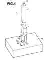
- Figure 4 is a perspective view that illustrates an initial stage of press fitting the compliant pin 1 into the aperture 102 of the circuit board 100.
- the press fit portion 2 is not in elastic contact with the circuit board 100 yet.
- the distal end portion 18 (refer to Figure 1) of the compliant pin 1 is inserted into the aperture 102, and the pressing surfaces 4a, 4a of the pressing portion 4 is pressed downward.
- arcuate outer peripheral surfaces 26a of the taper surfaces 22 frictionally contact the edge 102a of the aperture.
- the edge 102a and the inner surface of the aperture 102 are generally copper plated.
- the material of the compliant pin 1 is generally a copper alloy, which has good conductive properties.
- the copper alloy compliant pin 1 is plated with nickel, and tin plating is administered over the nickel plating.
- the thickness of the plating (metal) is generally 0.8 ⁇ m to 1.5 ⁇ m.
- the tin plating layer of the compliant pin 1 peels off along the insertion direction thereof, due to the frictional contact between the compliant pin 1 and the edge 102a of the aperture 102. That is, the portion of the taper surface 22 peels off along the central axis 10. At this time, shavings of plating forward (downward in Figure 4) of the recesses 28b are housed within the interior of the recesses 28b. When the compliant pin 1 is inserted further, the plating layer between the recesses 28b and the recesses 28a peel off, and the peeled off shavings are housed within the recesses 28a. Thereby, the compliant pin 1 is held in the aperture 102, in a state that the plating shavings are housed within the recesses 28a and 28b.
- plating shavings are most generated at the taper surfaces 22.
- shavings generated from the distal ends 22a to the rear ends 22b of the taper surfaces 22 are housed in the recesses 28a.
- the plating shavings are comparatively large, and the recesses 28a will house the large plating shavings.
- the additional recesses 28b are formed between the recesses 28a and the distal ends 22a of the taper surfaces 22.
- the peeled off plating shhavings
- the shavings are miniaturized, and become easier to house within the recesses 28a and 28b.
- the miniaturization of the shavings even in the case that the shavings become scattered outside the aperture 102, the possibility that they will cause short circuits and the like is reduced.
- the contact surface area between the taper surfaces 22 and the aperture 102 decreases, thereby reducing the amount of generated shavings.
- a greater number of recesses may be formed in the taper surfaces 22, in addition to the recesses 28a and 28b.
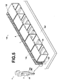
- FIG. 5 is a perspective view of a female connector 120 that utilizes a plurality of the compliant pins 1 of Figure 1. Note that the press fit portion 2 of a compliant pin 1 is enlarged.
- the connector 120 comprises: an insulative housing 122 (hereinafter, simply referred to as "housing"), which has an engaging recess 124 that opens toward the front; and the compliant pins 1. A great number of the compliant pins 1 are implanted in a rear wall 126 of the housing 122.
- the contact portions 6 of the compliant pins 1 are bent at a right angle, and mounted on the housing 122.
- the contact portions 6 protrude toward the interior of the engaging recess 124, to serve as electrical contact points with another connector (not shown).
- the connector 120 is mounted onto a circuit board 100', by press fitting the compliant pins 1 into apertures 102' of the circuit board 100'.
- the press fit portions 2 of the compliant pins 1 are arranged such that the swollen portions 2a are aligned perpendicular to the longitudinal direction of the housing 122.
- the plating on the compliant pin 1 may be of any metal, as long as it has conductive properties and corrosion resistance. Gold plating may be employed as necessary. However, particularly in the case that the plating is tin plating, the plating is comparatively soft. Therefore, the plating peels off easily during insertion of the compliant pin into the aperture, reducing the insertion resistance.
- the connector that utilizes the compliant pins 1 may be a male connector (not shown) that engages with the female connector 120. It goes without saying that the shape and size of the connector, as well as the number of compliant pins utilized therein, are changeable as well.
- the compliant pin 1 is tin plated. Therefore, the softer tin plating of the compliant pin 1 is more readily peeled off than the copper plating of the aperture 102.
- the present invention is applicable to cases other than that in which the plating of the compliant pin 1 peels off. Shavings can be housed within the recesses 28 of the compliant pin 1, when the plating of the aperture 102 peels off as well.
Landscapes
- Multi-Conductor Connections (AREA)
- Coupling Device And Connection With Printed Circuit (AREA)
Abstract
Description
- The present invention relates to a compliant pin, to be press fitted into a printed circuit board (hereinafter, simply referred to as "circuit board"), and an electrical connector that utilizes the compliant pin.
- Compliant pins are slightly elastically deformable in their radial directions. Therefore, when press fit portions thereof are pressed and inserted into apertures (through holes) of circuit boards, having slightly smaller diameters than those of the compliant pins, the compliant pins are fixed to the circuit board in a state of close contact, due to elastic deformation. Thereby, favorable electrical connections can be established without soldering. The inner surfaces of the apertures are generally copper plated, and the compliant pins are generally plated over their entire surfaces, for example, with tin plating. For this reason, plating shavings of tin plating, which is softer than copper plating, are generated during press fitting of the compliant pins, due to frictional contact between the compliant pins and the apertures. The plating shavings may be scattered on the circuit board, and there is a possibility that the scattered shavings will short printed circuits on the circuit board or electric/electronic components provided on the circuit board.
- Japanese Unexamined Patent Publication No. 6(1994)-013735 discloses a technique for solving the above problem. In this technique, plastic film is laminated on both sides of a circuit board, and the compliant pin is press fitted into the circuit board. The compliant pin is press fitted to penetrate the plastic film, and the plastic film surrounds the compliant film in a state of close contact. Thereby, the plating shavings generated during insertion are sealed within apertures of the circuit board, and scattering of the shavings on the circuit board is prevented.
- There is another known technique, in which a damp-proofing coating, for protecting electric/electronic components, is provided on both sides of a circuit board, into which compliant pins are press fitted. In this case, plating shavings are coated along with the electric/electronic components, so there is no possibility that the plating shavings will scatter. However, coating is not necessarily administered for all circuit boards.
- In the technique disclosed in Japanese Unexamined Patent Publication No. 6(1994)-013735, the plastic film for laminating the circuit board is necessary as a separate component. In addition, a laminating step becomes necessary. For this reason, the manufacturing process becomes troublesome, and costs are increased. Also in the technique that employs the damp-proofing coating, additional coating materials and a coating step become necessary.
- The present invention has been developed in view of the foregoing circumstances. It is an object of the present invention to provide a compliant pin and an electric connector that reduce the amount of plating shavings that scatter on a circuit board, without increasing components or manufacturing steps, and that miniaturizes the generated shavings, to prevent shorting between circuits on the circuit board and between electric/electronic devices.
- The compliant pin of the present invention is a compliant pin having a press fitted portion, to be press fit into an aperture of a circuit board, characterized by recesses formed in the press fit portion, for receiving metal shavings that result from contact with the aperture.
- A configuration may be adopted, wherein taper surfaces that converge toward a distal end of the compliant pin are formed on the press fit portion; and the recesses are formed in the taper surfaces.
- It is preferable that the recesses are formed in the vicinities of rear or proximal ends of the taper surfaces.
- At least one other recess may be formed between the recesses towards the rear or proximal ends of the taper surfaces and the distal ends of the taper surfaces.
- The metal shavings may be plating shavings, of plating formed on the compliant pin.
- A configuration may be adopted, wherein: the press fit portion comprises a pair of swollen portions that swell or protrude opposite to each other in the radial direction of the compliant pin; the swollen portions have sheared surfaces, formed by partial shearing along the central axis of the compliant pin; the taper surfaces have arcuate outer peripheral surfaces; and the recesses are formed in the arcuate outer peripheral surfaces.
- It is preferable that the recesses are formed from the distal end side of the compliant pin to the rear end side thereof, diagonal with respect to the longitudinal direction thereof, and inclined away from the sheared surfaces.
- It is preferable that the recesses are formed by molding, simultaneous with press molding of the compliant pin.
- The electrical connector of the present invention is a connector that utilizes any of the compliant pins according to the present invention.
- The compliant pin of the present invention has the recesses, for receiving the metallic shavings that result from contact with the aperture, formed in the press fit portion thereof. Therefore, the compliant pin and the electrical connector that utilizes the compliant pin exhibit the following advantageous effects. The metallic shavings are housed in the recesses, and not likely to be scattered on the circuit board. Therefore, the amount of shavings that scatter on the circuit board can be reduced. In addition, the generated shavings are miniaturized, thereby preventing shorting between circuits on the circuit board and between electric/electronic components on the circuit board. These advantageous effects are easily obtained, without additional components or additional steps for assembling the additional components.
- A configuration may be adopted, wherein taper surfaces that converge toward the distal end of the compliant pin are formed on the press fit portion; and the recesses are formed in the taper surfaces. In this case, the recesses are formed at the taper surfaces, where the greatest amount of shavings is generated. Therefore, the shavings are effectively housed in the recesses, reducing the possibility that they will be scattered on the circuit board.
- The recesses may be formed in the vicinities of the rear ends of the taper surfaces. In this case, the shavings which have peeled off from the taper surfaces can be consolidated and housed within the recesses, thereby preventing scattering thereof.
- At least one other recess may be formed between the recesses toward the rear of the taper surfaces and the distal ends of the taper surfaces. In this case, the shavings are segmented and miniaturized by the plurality of recesses. Thereby, the shavings can be further divided and housed within the plurality of recesses, further decreasing the likelihood that they will be scattered.
- The metal shavings may be plating shavings, of plating formed on the compliant pin. In this case, shavings from the portion of the compliant pin most likely to generate shavings when the compliant pin is inserted into the aperture can be effectively sealed within the recesses.
- The plating of the compliant pin may be tin plating. In this case, the plating is comparatively soft. Therefore, the plating peels off easily during insertion of the compliant pin into the aperture, reducing the insertion resistance.
- The invention will now be described by way of example only with reference to the accompanying drawings in which:
- Figures 1A, 1B, and 1C are magnified partial view of a press fit portion of a compliant pin according to the present invention, wherein Figure 1A is a plan view, Figure 1B is a side view, and Figure 1C is a front view.
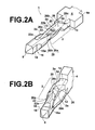
- Figures 2A and 2B illustrate the compliant pin of Figure 1, wherein Figure 2A is a perspective view corresponding to Figure 1A, and Figure 2B is a perspective view corresponding to Figure 1B.
- Figures 3A and 3B are magnified sectional views of the press fit portion of the compliant pin, wherein Figure 3A is a sectional view taken along line IIIA-IIIA of Figure 1A, and Figure 3B is a sectional view taken along line IIIB-IIIB of Figure 1A.
- Figure 4 is a perspective view that illustrates an initial stage of press fitting the compliant pin into an aperture of a circuit board.
- Figure 5 is a perspective view of a female connector that utilizes a plurality of the compliant pins of Figure 1.
- A description will be given with reference to Figures 1A through 2B.
- The
compliant pin 1 is a pin-shaped member formed by punching out a single metal plate. Thecompliant pin 1 comprises, in order from the distal end thereof: a press fit portion 2 (compliant portion); apressing portion 4; and a contact portion 6 (refer to Figure 4). Note that thecontact portion 6 is omitted from Figures 1A through 2B. Thepress fit portion 2 is formed toward thedistal end 8 of the compliant pin. Thepress fit portion 2 is formed by pressing amain body 1a of the compliant pin in opposite directions in a direction that perpendicularly intersects thecentral axis 10 of the compliant pin, to perform partial shearing such that the sheared portions swell or project in opposite directions from each other. Thepress fit portion 2 has slight elasticity in the radial direction (the direction along the plane of the sheared surfaces). Swollenportions surfaces 12 on one side thereof, are formed by the shearing operation. Thepress fit portion 2 is constituted by the pair of swollenportions 2a. Each of theswollen portions swollen portion 2a. - A
distal end portion 18 of thecompliant pin 1 comprises fourtapers 14 that converge at thedistal end 8.Flat surfaces 16 are formed continuous with a pair oftapers 14 that face each other. Thedistal end portion 18 is substantially square in cross-section.Inclined surfaces 16a that cause the cross-section of thecompliant pin 1 to increase toward themain body 1a are formed extending from the flat surfaces 16. - The
main body 1a is substantially rectangular in cross section. The pressfit portion 2 is sheared in a direction that perpendicularly intersects the long side of the rectangular cross section. The pressfit portion 2 comprises:parallel surfaces 20, which are positioned furthest toward the exterior and are substantially parallel to thecentral axis 10; taper surfaces 22 that incline from theparallel surfaces 20 toward thedistal end portion 18, and serve as guide surfaces during insertion of thecompliant pin 1; and taper surfaces 24, which are formed at the side of theparallel surfaces 20 opposite that of the taper surfaces 22. The parallel surfaces 20, the taper surfaces 22, and the taper surfaces 24 have arcuate outerperipheral surfaces peripheral surfaces peripheral surfaces outer surfaces 26". The arcuate outerperipheral surfaces 26 have arcuate shapes that conform to the arc or radius of curvature ofapertures 102 of a circuit board 100 (refer to Figure 4), into which thecompliant pin 1 is inserted. The arcuate outerperipheral surfaces 26 contact theapertures 102 with the greatest force. - Two recesses 28 (28a, 28b) are formed in each of the taper surfaces 22, between the distal ends 22a and the
rear ends 22b (shoulders) thereof. Therecesses 28a are formed in the vicinity of therear ends 22b, and therecesses 28b are formed between therecesses 28a and thedistal ends 22a. Therecesses swollen portions 2a, when theswollen portions 2a are formed by a pressing machine. The number ofrecesses 28 is not limited to two, and may be three or greater, depending on the size and shape of thecompliant pin 1. - Each of the
recesses recesses edge 102a of theaperture 102, when thecompliant pin 1 is pressed into theaperture 102. The details of therecesses 28 will be described later, with reference to Figures 3A, 3B, and 4. Apressing portion 4 is formed toward the rear of the pressfit portion 2, that is, toward the side opposite from thedistal end portion 18. Thepressing portion 4 is a parallelepiped having a rectangular cross section that extends in the same direction as that of themain body 1a. Pressingsurfaces 4a that face the rear at both sides of themain body 1a are formed on thepressing portion 4. - Next, the
recesses 28 will be described in further detail, with reference to Figures 3A and 3B. Figures 3A and 3B are magnified sectional views of the pressfit portion 2, wherein Figure 3A is a sectional view taken along line IIIA-IIIA of Figure 1A, and Figure 3B is a sectional view taken along line IIIB-IIIB of Figure 1A. Figures 3A and 3B clearly illustrate the positional relationship between the pair ofswollen portions main body 1a of thecompliant pin 1. Therecesses 28a are formed in the arcuate outerperipheral surfaces 26a, as illustrated in Figure 3A. Therecesses 28b are also formed in the arcuate outerperipheral surfaces 26a, as illustrated in Figure 3B. The functions of therecesses - Figure 4 is a perspective view that illustrates an initial stage of press fitting the
compliant pin 1 into theaperture 102 of thecircuit board 100. In this state, the pressfit portion 2 is not in elastic contact with thecircuit board 100 yet. From this state, the distal end portion 18 (refer to Figure 1) of thecompliant pin 1 is inserted into theaperture 102, and thepressing surfaces pressing portion 4 is pressed downward. Thereby, arcuate outerperipheral surfaces 26a of the taper surfaces 22 frictionally contact theedge 102a of the aperture. Theedge 102a and the inner surface of theaperture 102 are generally copper plated. Meanwhile, the material of thecompliant pin 1 is generally a copper alloy, which has good conductive properties. The copper alloycompliant pin 1 is plated with nickel, and tin plating is administered over the nickel plating. The thickness of the plating (metal) is generally 0.8µm to 1.5µm. - The tin plating layer of the
compliant pin 1 peels off along the insertion direction thereof, due to the frictional contact between thecompliant pin 1 and theedge 102a of theaperture 102. That is, the portion of thetaper surface 22 peels off along thecentral axis 10. At this time, shavings of plating forward (downward in Figure 4) of therecesses 28b are housed within the interior of therecesses 28b. When thecompliant pin 1 is inserted further, the plating layer between therecesses 28b and therecesses 28a peel off, and the peeled off shavings are housed within therecesses 28a. Thereby, thecompliant pin 1 is held in theaperture 102, in a state that the plating shavings are housed within therecesses - What is important to note here is that plating shavings are most generated at the taper surfaces 22. In order to prevent the shavings generated at the taper surfaces 22 from scattering, it is necessary to provide the
recesses 28a at least at the rear ends 22b of the taper surfaces 22. In this case, shavings generated from the distal ends 22a to the rear ends 22b of the taper surfaces 22 are housed in therecesses 28a. In this case, the plating shavings are comparatively large, and therecesses 28a will house the large plating shavings. - For this reason, it is preferable that the
additional recesses 28b are formed between therecesses 28a and the distal ends 22a of the taper surfaces 22. By providing theadditional recesses 28b, the peeled off plating (shavings) are divided into those having lengths between the distal ends 22a of the taper surfaces 22 to therecesses 28b, and those having lengths between therecesses 28a and therecesses 28a. Therefore, the shavings are miniaturized, and become easier to house within therecesses aperture 102, the possibility that they will cause short circuits and the like is reduced. Further, by the presence of theadditional recesses 28b, the contact surface area between the taper surfaces 22 and theaperture 102 decreases, thereby reducing the amount of generated shavings. A greater number of recesses may be formed in the taper surfaces 22, in addition to therecesses - Next, an electrical connector (hereinafter, simply referred to as "connector") that utilizes the
compliant pin 1 will be described with reference to Figure 5. Figure 5 is a perspective view of afemale connector 120 that utilizes a plurality of thecompliant pins 1 of Figure 1. Note that the pressfit portion 2 of acompliant pin 1 is enlarged. Theconnector 120 comprises: an insulative housing 122 (hereinafter, simply referred to as "housing"), which has anengaging recess 124 that opens toward the front; and the compliant pins 1. A great number of thecompliant pins 1 are implanted in arear wall 126 of thehousing 122. - The
contact portions 6 of thecompliant pins 1 are bent at a right angle, and mounted on thehousing 122. Thecontact portions 6 protrude toward the interior of theengaging recess 124, to serve as electrical contact points with another connector (not shown). Theconnector 120 is mounted onto a circuit board 100', by press fitting thecompliant pins 1 into apertures 102' of the circuit board 100'. Thepress fit portions 2 of thecompliant pins 1 are arranged such that theswollen portions 2a are aligned perpendicular to the longitudinal direction of thehousing 122. - The plating on the
compliant pin 1 may be of any metal, as long as it has conductive properties and corrosion resistance. Gold plating may be employed as necessary. However, particularly in the case that the plating is tin plating, the plating is comparatively soft. Therefore, the plating peels off easily during insertion of the compliant pin into the aperture, reducing the insertion resistance. - Embodiments of the present invention have been described above. However, the present invention is not limited to the above embodiments. Various changes and modifications are possible as long as they do not depart from the scope of the invention. For example, the connector that utilizes the
compliant pins 1 may be a male connector (not shown) that engages with thefemale connector 120. It goes without saying that the shape and size of the connector, as well as the number of compliant pins utilized therein, are changeable as well. - In addition, in the embodiments described above, the
compliant pin 1 is tin plated. Therefore, the softer tin plating of thecompliant pin 1 is more readily peeled off than the copper plating of theaperture 102. However, the present invention is applicable to cases other than that in which the plating of thecompliant pin 1 peels off. Shavings can be housed within therecesses 28 of thecompliant pin 1, when the plating of theaperture 102 peels off as well.
Claims (7)
- A compliant pin (1), comprising:a press fit portion (2) to be press fitted into an aperture (102, 102') of a circuit board (100, 100'); characterized by:recesses (28a, 28b) formed in the press fit portion (2), for receiving metal shavings that result from contact with the aperture (102, 102').
- A compliant pin (1) as defined in claim 1, wherein taper surfaces (22) that converge toward a distal end (8) of the compliant pin (1) are formed on the press fit portion (2) and the recesses (28a, 28b) are formed in the taper surfaces (22).
- A compliant pin (1) as defined in claim 2, wherein the recesses (28a) are formed in the taper surfaces (22) in the vicinities of rear or proximal ends (22b) thereof.
- A compliant pin (1) as defined in claim 3, further comprising at least one other recess (28b), formed between one said recess (28a) and a distal end (22a) of its associated taper surfaces (22).
- A compliant pin (1) as defined in any preceding claim 1, wherein the metal shavings are shavings of plating which is formed on the compliant pin (1).
- A compliant pin (1) as defined in claim 5, wherein the plating on the compliant pin (1) is tin plating.
- An electrical connector that utilizes the compliant pin (1) defined in any one of claims 1 through 6.
Applications Claiming Priority (1)
| Application Number | Priority Date | Filing Date | Title |
|---|---|---|---|
| JP2004235286A JP2006054116A (en) | 2004-08-12 | 2004-08-12 | Compliant pin and electric connector using compliant pin |
Publications (2)
| Publication Number | Publication Date |
|---|---|
| EP1626460A2 true EP1626460A2 (en) | 2006-02-15 |
| EP1626460A3 EP1626460A3 (en) | 2007-06-27 |
Family
ID=35107060
Family Applications (1)
| Application Number | Title | Priority Date | Filing Date |
|---|---|---|---|
| EP05107327A Pending EP1626460A3 (en) | 2004-08-12 | 2005-08-09 | Compliant pin and electrical connector utilizing compliant pin |
Country Status (3)
| Country | Link |
|---|---|
| US (1) | US7074094B2 (en) |
| EP (1) | EP1626460A3 (en) |
| JP (1) | JP2006054116A (en) |
Cited By (3)
| Publication number | Priority date | Publication date | Assignee | Title |
|---|---|---|---|---|
| EP1944834A3 (en) * | 2007-01-10 | 2009-05-13 | Delphi Technologies, Inc. | Compliant pin |
| CN107453077A (en) * | 2016-05-30 | 2017-12-08 | 住友电装株式会社 | Substrate terminal |
| CN110247212A (en) * | 2018-03-09 | 2019-09-17 | 株式会社电装 | Press-fit terminals and method for manufacturing press-fit terminals |
Families Citing this family (32)
| Publication number | Priority date | Publication date | Assignee | Title |
|---|---|---|---|---|
| KR100704971B1 (en) | 2005-01-21 | 2007-04-10 | 타이코에이엠피 주식회사 | Double PCB with Solderless Connection |
| US7377823B2 (en) * | 2005-05-23 | 2008-05-27 | J.S.T. Corporation | Press-fit pin |
| US7249981B2 (en) | 2005-07-08 | 2007-07-31 | J.S.T. Corporation | Press-fit pin |
| US7549897B2 (en) * | 2006-08-02 | 2009-06-23 | Tyco Electronics Corporation | Electrical connector having improved terminal configuration |
| US7591655B2 (en) * | 2006-08-02 | 2009-09-22 | Tyco Electronics Corporation | Electrical connector having improved electrical characteristics |
| US8142236B2 (en) * | 2006-08-02 | 2012-03-27 | Tyco Electronics Corporation | Electrical connector having improved density and routing characteristics and related methods |
| US7670196B2 (en) * | 2006-08-02 | 2010-03-02 | Tyco Electronics Corporation | Electrical terminal having tactile feedback tip and electrical connector for use therewith |
| US7413484B2 (en) * | 2006-08-02 | 2008-08-19 | Tyco Electronics Corporation | Electrical terminal having a compliant retention section |
| US7753742B2 (en) | 2006-08-02 | 2010-07-13 | Tyco Electronics Corporation | Electrical terminal having improved insertion characteristics and electrical connector for use therewith |
| US7458274B2 (en) * | 2007-02-20 | 2008-12-02 | Honeywell International Inc. | Pressure sensor incorporating a compliant pin |
| US20080318453A1 (en) * | 2007-06-20 | 2008-12-25 | Dancison Philip M | Compliant pin |
| US7957156B2 (en) * | 2007-08-06 | 2011-06-07 | Lear Corporation | Busbar circuit board assembly |
| DE102007044412A1 (en) * | 2007-09-18 | 2009-03-19 | Lear Corp., Southfield | Electrical connector assembly |
| US7862376B2 (en) * | 2008-09-23 | 2011-01-04 | Tyco Electronics Corporation | Compliant pin for retaining and electrically connecting a shield with a connector assembly |
| DE102008064590B3 (en) * | 2008-12-19 | 2010-07-15 | Tyco Electronics Amp Gmbh | Contact arrangement for connection to a polygonal socket |
| JP5224067B2 (en) * | 2009-11-11 | 2013-07-03 | 住友電装株式会社 | Board terminal and board connector having the same |
| US8221132B2 (en) * | 2010-08-25 | 2012-07-17 | Tyco Electronics Corporation | Electrical connector assembly |
| US8092262B1 (en) | 2010-10-15 | 2012-01-10 | Tyco Electronics Corporation | Eye-of-the needle pin of an electrical contact |
| JP2013131364A (en) * | 2011-12-21 | 2013-07-04 | Sumitomo Wiring Syst Ltd | Terminal fitting and terminal fitting connection structure |
| US9402320B2 (en) | 2012-11-15 | 2016-07-26 | International Business Machines Corporation | Electronic component assembly |
| US9449753B2 (en) | 2013-08-30 | 2016-09-20 | Qualcomm Incorporated | Varying thickness inductor |
| JP6103380B2 (en) * | 2013-09-03 | 2017-03-29 | 住友電装株式会社 | Board terminal |
| JP6550890B2 (en) * | 2015-04-22 | 2019-07-31 | 住友電装株式会社 | Press-fit terminal |
| JP2017174642A (en) * | 2016-03-24 | 2017-09-28 | 矢崎総業株式会社 | Press-fit terminal |
| KR101942812B1 (en) * | 2017-07-18 | 2019-01-29 | 제엠제코(주) | Press pin amd semiconductor package having the same |
| JP7027932B2 (en) * | 2018-02-14 | 2022-03-02 | 住友電装株式会社 | Press-fit terminal |
| JP7099020B2 (en) * | 2018-04-10 | 2022-07-12 | 株式会社デンソー | Press-fit terminals and electronic devices including press-fit terminals |
| JP2020031153A (en) * | 2018-08-23 | 2020-02-27 | トヨタ自動車株式会社 | Semiconductor device |
| JP7135632B2 (en) | 2018-09-13 | 2022-09-13 | 住友電装株式会社 | PRESS-FIT TERMINAL AND METHOD FOR MANUFACTURING PRESS-FIT TERMINAL |
| US11050208B2 (en) | 2018-10-31 | 2021-06-29 | International Business Machines Corporation | Pre-screening, compliant pin guiding and quality monitoring press-fit apparatus |
| KR102178119B1 (en) | 2018-12-07 | 2020-11-12 | 제엠제코(주) | Press-fit pin, semiconductor package having the same and method for manufacturing the press-fit pin |
| DE102019112617A1 (en) * | 2019-05-14 | 2020-11-19 | Te Connectivity Germany Gmbh | Connecting pin and method of making a connecting pin |
Citations (1)
| Publication number | Priority date | Publication date | Assignee | Title |
|---|---|---|---|---|
| JP2004165161A (en) | 2002-11-13 | 2004-06-10 | Tyco Electronics Amp Gmbh | Plug connecting device, contact pin for plug connecting device and receptacle element for plug connecting device |
Family Cites Families (12)
| Publication number | Priority date | Publication date | Assignee | Title |
|---|---|---|---|---|
| US4186982A (en) * | 1973-08-01 | 1980-02-05 | Amp Incorporated | Contact with split portion for engagement with substrate |
| US4606589A (en) * | 1984-01-12 | 1986-08-19 | H & V Services | Compliant pin |
| DE3513768A1 (en) * | 1985-04-17 | 1986-10-23 | Standard Elektrik Lorenz Ag, 7000 Stuttgart | METHOD FOR PRODUCING AN ELECTRICAL CONTACT PIN FOR PRINTED CIRCUIT BOARDS AND TOOL FOR IMPLEMENTING THE METHOD |
| CH675929A5 (en) * | 1988-05-06 | 1990-11-15 | Cdm Connectors Dev & Mfg Ag | |
| DE69022062T2 (en) * | 1990-12-31 | 1996-05-09 | Zierick Mfg Corp | Electrical end connector with breakable assembly pin and manufacturing process therefor. |
| JPH0613735A (en) * | 1992-06-25 | 1994-01-21 | Hitachi Ltd | Printed board |
| JPH06151035A (en) * | 1992-09-21 | 1994-05-31 | Matsushita Electric Works Ltd | Joining of lead terminal to circuit subtrate |
| JP2803574B2 (en) * | 1994-08-30 | 1998-09-24 | 日本電気株式会社 | Press-in terminal of connector and method of manufacturing the same |
| US5980271A (en) * | 1998-04-15 | 1999-11-09 | Hon Hai Precision Ind. Co., Ltd. | Header connector of a future bus and related compliant pins |
| JP3361757B2 (en) * | 1998-10-29 | 2003-01-07 | 第一電子工業株式会社 | Press-in contact |
| JP3390721B2 (en) * | 2000-03-09 | 2003-03-31 | 第一電子工業株式会社 | C-type compliant contact |
| DE10045233A1 (en) * | 2000-09-13 | 2002-03-28 | Bosch Gmbh Robert | Terminal pin, sleeve and electrically conductive connection |
-
2004
- 2004-08-12 JP JP2004235286A patent/JP2006054116A/en active Pending
-
2005
- 2005-08-09 EP EP05107327A patent/EP1626460A3/en active Pending
- 2005-08-12 US US11/203,054 patent/US7074094B2/en not_active Expired - Fee Related
Patent Citations (1)
| Publication number | Priority date | Publication date | Assignee | Title |
|---|---|---|---|---|
| JP2004165161A (en) | 2002-11-13 | 2004-06-10 | Tyco Electronics Amp Gmbh | Plug connecting device, contact pin for plug connecting device and receptacle element for plug connecting device |
Cited By (4)
| Publication number | Priority date | Publication date | Assignee | Title |
|---|---|---|---|---|
| EP1944834A3 (en) * | 2007-01-10 | 2009-05-13 | Delphi Technologies, Inc. | Compliant pin |
| CN107453077A (en) * | 2016-05-30 | 2017-12-08 | 住友电装株式会社 | Substrate terminal |
| CN110247212A (en) * | 2018-03-09 | 2019-09-17 | 株式会社电装 | Press-fit terminals and method for manufacturing press-fit terminals |
| DE102019104400B4 (en) | 2018-03-09 | 2025-01-30 | Denso Corporation | Method for producing a press-fit contact |
Also Published As
| Publication number | Publication date |
|---|---|
| US20060035535A1 (en) | 2006-02-16 |
| JP2006054116A (en) | 2006-02-23 |
| US7074094B2 (en) | 2006-07-11 |
| EP1626460A3 (en) | 2007-06-27 |
Similar Documents
| Publication | Publication Date | Title |
|---|---|---|
| EP1626460A2 (en) | Compliant pin and electrical connector utilizing compliant pin | |
| CN100482033C (en) | Connection structure of printed wiring board | |
| CN100531513C (en) | Connecting device for printed wiring board | |
| JP4676502B2 (en) | Board to board connector | |
| US5035656A (en) | Connector, circuit board contact element and retention portion | |
| EP2913897B1 (en) | Connector structure, female connector and male connector | |
| CN100534260C (en) | Connecting device for printed wiring board | |
| WO2005096445A1 (en) | Connector | |
| JPH08190968A (en) | Connector having metal strip as contact member and connector assembly including the connector | |
| WO2005096456A1 (en) | Connector | |
| US10680360B2 (en) | Press-fit terminal and electronic device including press-fit terminal | |
| US5129830A (en) | Z-axis pin connectors for stacked printed circuit board assemblies | |
| US5120257A (en) | Lanced hold-downs | |
| US5083928A (en) | Electrical pin tips | |
| US20040127097A1 (en) | Ground bus for an electrical connector | |
| US6960094B2 (en) | Flat and thin connector for electrically connecting a flexible printed circuit board and a hard board | |
| US8371871B1 (en) | Terminal with compliant barb | |
| WO2008051354A2 (en) | Press-fit electrical contact | |
| CN101529661A (en) | Connector | |
| US5916000A (en) | Press fit electrical contact | |
| KR19990068028A (en) | Terminal Pins Mounted in Flexible Substrate | |
| US11394143B2 (en) | Connector | |
| US20040147145A1 (en) | Straddle-mount electrical connector | |
| US20090298345A1 (en) | Connector | |
| US20030190827A1 (en) | Electrical connector having retention contact tails and non-retention contact tails for retaining to a pcb prior to soldering as well as reducing force of inserting the contact tails to the pcb |
Legal Events
| Date | Code | Title | Description |
|---|---|---|---|
| PUAI | Public reference made under article 153(3) epc to a published international application that has entered the european phase |
Free format text: ORIGINAL CODE: 0009012 |
|
| AK | Designated contracting states |
Kind code of ref document: A2 Designated state(s): AT BE BG CH CY CZ DE DK EE ES FI FR GB GR HU IE IS IT LI LT LU LV MC NL PL PT RO SE SI SK TR |
|
| AX | Request for extension of the european patent |
Extension state: AL BA HR MK YU |
|
| PUAL | Search report despatched |
Free format text: ORIGINAL CODE: 0009013 |
|
| AK | Designated contracting states |
Kind code of ref document: A3 Designated state(s): AT BE BG CH CY CZ DE DK EE ES FI FR GB GR HU IE IS IT LI LT LU LV MC NL PL PT RO SE SI SK TR |
|
| AX | Request for extension of the european patent |
Extension state: AL BA HR MK YU |
|
| 17P | Request for examination filed |
Effective date: 20071221 |
|
| AKX | Designation fees paid |
Designated state(s): DE FR GB |
|
| 17Q | First examination report despatched |
Effective date: 20080206 |
|
| R17C | First examination report despatched (corrected) |
Effective date: 20080215 |
|
| GRAP | Despatch of communication of intention to grant a patent |
Free format text: ORIGINAL CODE: EPIDOSNIGR1 |
|
| STAA | Information on the status of an ep patent application or granted ep patent |
Free format text: STATUS: GRANT OF PATENT IS INTENDED |
|
| RAP1 | Party data changed (applicant data changed or rights of an application transferred) |
Owner name: TYCO ELECTRONICS JAPAN G.K. |