US20030190827A1 - Electrical connector having retention contact tails and non-retention contact tails for retaining to a pcb prior to soldering as well as reducing force of inserting the contact tails to the pcb - Google Patents
Electrical connector having retention contact tails and non-retention contact tails for retaining to a pcb prior to soldering as well as reducing force of inserting the contact tails to the pcb Download PDFInfo
- Publication number
- US20030190827A1 US20030190827A1 US10/120,003 US12000302A US2003190827A1 US 20030190827 A1 US20030190827 A1 US 20030190827A1 US 12000302 A US12000302 A US 12000302A US 2003190827 A1 US2003190827 A1 US 2003190827A1
- Authority
- US
- United States
- Prior art keywords
- tail portions
- sets
- protrusions
- contacts
- electrical connector
- Prior art date
- Legal status (The legal status is an assumption and is not a legal conclusion. Google has not performed a legal analysis and makes no representation as to the accuracy of the status listed.)
- Granted
Links
Images


Classifications
-
- H—ELECTRICITY
- H05—ELECTRIC TECHNIQUES NOT OTHERWISE PROVIDED FOR
- H05K—PRINTED CIRCUITS; CASINGS OR CONSTRUCTIONAL DETAILS OF ELECTRIC APPARATUS; MANUFACTURE OF ASSEMBLAGES OF ELECTRICAL COMPONENTS
- H05K3/00—Apparatus or processes for manufacturing printed circuits
- H05K3/30—Assembling printed circuits with electric components, e.g. with resistors
- H05K3/306—Assembling printed circuits with electric components, e.g. with resistors with lead-in-hole components
- H05K3/308—Adaptations of leads
-
- H—ELECTRICITY
- H01—ELECTRIC ELEMENTS
- H01R—ELECTRICALLY-CONDUCTIVE CONNECTIONS; STRUCTURAL ASSOCIATIONS OF A PLURALITY OF MUTUALLY-INSULATED ELECTRICAL CONNECTING ELEMENTS; COUPLING DEVICES; CURRENT COLLECTORS
- H01R12/00—Structural associations of a plurality of mutually-insulated electrical connecting elements, specially adapted for printed circuits, e.g. printed circuit boards [PCB], flat or ribbon cables, or like generally planar structures, e.g. terminal strips, terminal blocks; Coupling devices specially adapted for printed circuits, flat or ribbon cables, or like generally planar structures; Terminals specially adapted for contact with, or insertion into, printed circuits, flat or ribbon cables, or like generally planar structures
- H01R12/70—Coupling devices
- H01R12/7005—Guiding, mounting, polarizing or locking means; Extractors
- H01R12/7011—Locking or fixing a connector to a PCB
- H01R12/7017—Snap means
Definitions
- the present invention relates to the technology of manufacturing an electrical connector, and particularly to the technology of manufacturing the electrical connector having retention contact tails for retaining the connector onto a printed circuit board (PCB) before the connector is soldered onto the PCB and non-retention contacts tails for reducing the force of inserting the contact tails to the PCB.
- PCB printed circuit board
- Typical board retention designs require an interference feature into a hole on a printed circuit board (PCB). This can be accomplished with separate retention pins, for example, and board locks. Separate retention pins add to the overall product cost and take up extra space thereby adding to the size of the connectors. So, there is a trend of using contact tails to accomplish the retention feature. In order to keep manufacturing and assembly costs minimal, typically all retention pins exhibit the same geometry. This leads to having all the contact tails provide retention but not all. This approach has the negative impact of increasing the insertion force. Ideally, it would be beneficial to have some contact tails accomplish the retention feature and the other contact tails do not accomplish the retention feature, thereby permitting flexibility in the insertion and retention characteristics of the connectors.
- U.S. Pat. No. 5,411,404 issued to THE WHITAKER CORPORATION, discloses an electrical connector having contact tails with retention feature and contact tails without retention feature.
- the retention feature contact tails and the non-retention feature contact tails have different geometries created by hard tooling, dies, and the geometries cannot be readily changed from one to the other. This adds to the manufacturing cost of the connector.
- an improved electrical connector whose retention feature contact tails and the non-retention feature contact tails can be created in the same tools will overcome the disadvantage of the prior art.
- a first objective of the present invention is to provide an electrical connector having conductive contacts, some of which have a retention feature while others do not have a retention feature and both can be manufactured in the same tools, thereby reducing the manufacturing cost.
- a second objective of the present invention is to provide an electronic device including a printed circuit board (PCB) and the aforementioned electrical connector retained onto the PCB.
- PCB printed circuit board
- a third objective of the present invention is to provide a method of manufacturing the conductive contacts of the aforementioned electrical connector.
- an electrical connector including an insulative housing and a plurality of contacts attached to the housing was invented.
- the contacts each have a contact tail downwardly extending beyond a mounting surface of the insulative housing for inserting into a throughhole of the PCB.
- the contact tails are overlapped in pairs and each pair of contact tails is inserted into the same throughhole of the PCB.
- Some pairs of contact tails called retention contact tails, have protrusions deviating from each other for bearing against the peripheral walls of the throughholes of the PCB thereby producing retention force.
- the other pairs of contact tails called non-retention contact tails, do not have protrusions and do not interfere with the peripheral walls of the other throughholes of the PCB thereby producing no retention force.
- the retention contact tails can be modified to be non-retention contact tails by deforming the protrusions.
- the protrusions are sheared off.
- a portion of the contact tip having the protrusions is removed to provide a lead in chamfer for aiding in alignment of the contact tails to the holes of the PCB.
- the protrusions are swaged into notches of the other corresponding contact tails.
- the tail portions may be embedded in the plated holes or extend through the PC board, which is determined by thickness of the PC board and the length of the tail portions.
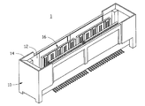
- FIG. 1 is a perspective view of a board mountable electrical connector in accordance with the present invention
- FIG. 2 is an enlarged perspective view of a part of the electrical connector in FIG. 1;
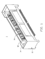
- FIG. 3 is similar to FIG. 2 but viewed from a different angle
- FIG. 4 is a cross-sectional view of the connector shown in FIG. 1 and a printed circuit board (PCB) on which the connector is mounted;
- PCB printed circuit board
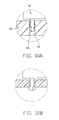
- FIGS. 5 A- 5 C are partially enlarged perspective view of the contact tails of the connector which respectively illustrate three different geometries of the contact tails;
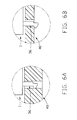
- FIG. 6 is a planar view of the connector mounted onto the PCB, wherein the PCB is cross-sectioned to illustrate the engagement of the contact tails with holes of the PCB;
- FIG. 6A is an enlarged view of a circled part in FIG. 6 and FIG. 6B is an alternative condition of FIG. 6A;
- FIG. 7 is a view similar to FIG. 4 but illustrates a second embodiment of the present invention.
- FIGS. 8 A- 8 D are enlarged perspective views of the contact tails of the second embodiment of the present invention which illustrate four geometries of the contacts tails;
- FIGS. 9 A- 9 D are planar views of FIGS. 8 A- 8 D, respectively;
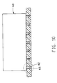
- FIG. 10 is a view similar to FIG. 6 but illustrates the second embodiment of the present invention.
- FIG. 10A is an enlarged view of a circled part of FIG. 10 and FIG. 10B is an alternative condition of FIG. 10A;
- FIG. 11 is a view similar to FIG. 3 but illustrates a third embodiment of the connector of the present invention.
- an electrical connector 1 in accordance with the present invention comprises an insulative housing 10 defining a center slot 12 in an upper surface 14 thereof and several terminal modules 16 (four modules are preferably shown in FIG. 1) fixedly received in the center slot 12 of the housing 10 and arranged in two rows.
- Each terminal module 16 includes an insulative insert 18 and a plurality of signal contacts 20 and several grounding contacts 22 respectively attached to opposite surfaces 24 , 26 of the insert 18 .
- Each signal contact 20 has a mating portion 28 in the center slot 12 adapted for electrically engaging with a corresponding conductor of a mating connector (not shown) and a mounting tail portion 30 extending beyond a mounting surface 32 of the housing adapted for mounting to a corresponding conductive pad 38 on a PC board 40 .
- each grounding contact 22 has a mating portion 34 in the center slot 12 and a mounting tail portion 36 extending beyond the mounting surface 32 for engageably received in a plated hole 42 of the PC board 40 .
- the tail portions 36 of the grounding contacts 22 include retention pin type tails 44 and non-retention pin type tails 46 arranged along a longitudinal direction of the housing in a manner that one retention pin type tail 44 is followed by several non-retention pin type tails 46 .
- the retention pin type tails 44 each have a larger size than the non-retention pin type tails 46 or a protrusion so that when the tail portions 36 are received in corresponding plated holes 42 , the retention pin type tails 44 engage with peripheral walls of the plated holes 42 and produce retention force for maintaining the connector 1 to the PC board 40 while the non-retention pin type tails 46 do not (FIG.
- the retention force is adjustable by changing the number of the retention pin type tails 44 .
- the retention pin type tail 44 defines a notch 48 at a side 50 thereof and has a barb 52 protruding outwardly from an opposite side 54 thereof.
- the non-retention pin type tail 46 may be modified from the retention pin type tail 44 by severing the barb 52 from the retention pin type tail 44 (shown by broken lines).
- FIG. 5C shows a second geometry of the non-retention pin type contact 47 which is modified from the retention pin type tail 44 by severing a tip portion containing the barb 52 to define a lead in chamfer for aiding in alignment of the non-retention pin type contact 47 to the hole 42 of the PCB 40 .
- the retention pin type tails 44 interfere with the plated walls 42 and deflect which produces a retention force therebetween.
- the non-retention pin type tails 46 do not interfere with the plated holes 42 and no retention force is produced therebetween.
- the retention pin type tails 44 will increase the insertion force for attaching the connector 1 to the PC board 40 .
- the insertion force can be controlled to an acceptable degree by reducing the number of retention pin type tails 44 .
- the tail portions 44 , 46 may be embedded in the plated holes 42 or extend through the PC board 40 , which is determined by thickness of the PC board 40 and the length of the tail portions 44 , 46 .
- FIG. 7 illustrates an electrical connector 60 in accordance with a second embodiment of the present invention.
- This connector 60 is similar to the connector 1 of the first embodiment except that corresponding tail portions 62 of two rows of grounding contacts 64 deflect toward each other and overlap back to back to form overlapped tail portions 66 .
- Each overlapped tail portion is received in the same plated hole 42 of the PC board 40 .
- the overlapped tail portions 66 include retention pin type 68 and non-retention pin type 70 .
- Each retention pin type overlapped tail portion 68 includes two retention pin type tail portions 44 overlapped in a manner that the barbs 52 thereof are away from each other.
- Each non-retention pin type overlapped tail portion 70 includes two non-retention pin type tail portions 46 overlapped in a manner that the notches 48 thereof are away from each other.
- the retention pin type overlapped tail portions 68 may be further processed to become the non-retention pin type overlapped tail portions 70 simply by severing the barbs 52 therefrom (FIGS. 5B and 5C).
- the non-retention pin type overlapped tail portions have a second geometry designated by 70 ′ in FIGS. 8C and 9C produced by trimming the rip of the lead.
- the barbs 52 may also be deformed into corresponding notches 48 to form a third geometry designated by 70 ′′ in FIGS. 8D and 9D.
- FIGS. 10, 10A and 10 B when mounting to a thicker PC board 40 , the retention pin type overlapped tail portions 68 are embedded in the plated holes and biased by the peripheral walls of the plated holes to deflect in opposite directions.
- the retention pin type overlapped tail portions 68 are inserted through the plated holes and bearing against a bottom surface of the thinner PC board 40 ′.
- FIG. 11 illustrates a third embodiment of the present invention.
- the signal contacts 20 are throughhole type and above-mentioned retention pin structures are applied to the tail portions 30 of the signal contacts 20 instead of the tail portions 36 of the grounding contacts 22 .
Landscapes
- Engineering & Computer Science (AREA)
- Manufacturing & Machinery (AREA)
- Microelectronics & Electronic Packaging (AREA)
- Coupling Device And Connection With Printed Circuit (AREA)
- Multi-Conductor Connections (AREA)
Abstract
Description
- 1. Field of the Invention
- The present invention relates to the technology of manufacturing an electrical connector, and particularly to the technology of manufacturing the electrical connector having retention contact tails for retaining the connector onto a printed circuit board (PCB) before the connector is soldered onto the PCB and non-retention contacts tails for reducing the force of inserting the contact tails to the PCB.
- 2. Description of the Related Art
- Typical board retention designs require an interference feature into a hole on a printed circuit board (PCB). This can be accomplished with separate retention pins, for example, and board locks. Separate retention pins add to the overall product cost and take up extra space thereby adding to the size of the connectors. So, there is a trend of using contact tails to accomplish the retention feature. In order to keep manufacturing and assembly costs minimal, typically all retention pins exhibit the same geometry. This leads to having all the contact tails provide retention but not all. This approach has the negative impact of increasing the insertion force. Ideally, it would be beneficial to have some contact tails accomplish the retention feature and the other contact tails do not accomplish the retention feature, thereby permitting flexibility in the insertion and retention characteristics of the connectors.
- U.S. Pat. No. 5,411,404, issued to THE WHITAKER CORPORATION, discloses an electrical connector having contact tails with retention feature and contact tails without retention feature. However, the retention feature contact tails and the non-retention feature contact tails have different geometries created by hard tooling, dies, and the geometries cannot be readily changed from one to the other. This adds to the manufacturing cost of the connector. Hence, an improved electrical connector whose retention feature contact tails and the non-retention feature contact tails can be created in the same tools will overcome the disadvantage of the prior art.
- A first objective of the present invention is to provide an electrical connector having conductive contacts, some of which have a retention feature while others do not have a retention feature and both can be manufactured in the same tools, thereby reducing the manufacturing cost.
- A second objective of the present invention is to provide an electronic device including a printed circuit board (PCB) and the aforementioned electrical connector retained onto the PCB.
- A third objective of the present invention is to provide a method of manufacturing the conductive contacts of the aforementioned electrical connector.
- To fulfill the above objectives, an electrical connector including an insulative housing and a plurality of contacts attached to the housing was invented. The contacts each have a contact tail downwardly extending beyond a mounting surface of the insulative housing for inserting into a throughhole of the PCB. The contact tails are overlapped in pairs and each pair of contact tails is inserted into the same throughhole of the PCB. Some pairs of contact tails, called retention contact tails, have protrusions deviating from each other for bearing against the peripheral walls of the throughholes of the PCB thereby producing retention force. The other pairs of contact tails, called non-retention contact tails, do not have protrusions and do not interfere with the peripheral walls of the other throughholes of the PCB thereby producing no retention force. The retention contact tails can be modified to be non-retention contact tails by deforming the protrusions. In the first embodiment, the protrusions are sheared off. In the second embodiment, a portion of the contact tip having the protrusions is removed to provide a lead in chamfer for aiding in alignment of the contact tails to the holes of the PCB. In the third embodiment, the protrusions are swaged into notches of the other corresponding contact tails. The tail portions may be embedded in the plated holes or extend through the PC board, which is determined by thickness of the PC board and the length of the tail portions.
- Other objectives, advantages and novel features of the invention will become more apparent from the following detailed description of the present embodiment when taken in conjunction with the accompanying drawings.
- FIG. 1 is a perspective view of a board mountable electrical connector in accordance with the present invention;
- FIG. 2 is an enlarged perspective view of a part of the electrical connector in FIG. 1;
- FIG. 3 is similar to FIG. 2 but viewed from a different angle;
- FIG. 4 is a cross-sectional view of the connector shown in FIG. 1 and a printed circuit board (PCB) on which the connector is mounted;
- FIGS. 5A-5C are partially enlarged perspective view of the contact tails of the connector which respectively illustrate three different geometries of the contact tails;
- FIG. 6 is a planar view of the connector mounted onto the PCB, wherein the PCB is cross-sectioned to illustrate the engagement of the contact tails with holes of the PCB;
- FIG. 6A is an enlarged view of a circled part in FIG. 6 and FIG. 6B is an alternative condition of FIG. 6A;
- FIG. 7 is a view similar to FIG. 4 but illustrates a second embodiment of the present invention;
- FIGS. 8A-8D are enlarged perspective views of the contact tails of the second embodiment of the present invention which illustrate four geometries of the contacts tails;
- FIGS. 9A-9D are planar views of FIGS. 8A-8D, respectively;
- FIG. 10 is a view similar to FIG. 6 but illustrates the second embodiment of the present invention;
- FIG. 10A is an enlarged view of a circled part of FIG. 10 and FIG. 10B is an alternative condition of FIG. 10A; and
- FIG. 11 is a view similar to FIG. 3 but illustrates a third embodiment of the connector of the present invention.
- Referring to FIGS. 1-4, an
electrical connector 1 in accordance with the present invention comprises aninsulative housing 10 defining acenter slot 12 in anupper surface 14 thereof and several terminal modules 16 (four modules are preferably shown in FIG. 1) fixedly received in thecenter slot 12 of thehousing 10 and arranged in two rows. Eachterminal module 16 includes aninsulative insert 18 and a plurality of signal contacts 20 andseveral grounding contacts 22 respectively attached toopposite surfaces insert 18. Each signal contact 20 has a mating portion 28 in thecenter slot 12 adapted for electrically engaging with a corresponding conductor of a mating connector (not shown) and amounting tail portion 30 extending beyond amounting surface 32 of the housing adapted for mounting to a correspondingconductive pad 38 on aPC board 40. Similarly, eachgrounding contact 22 has amating portion 34 in thecenter slot 12 and amounting tail portion 36 extending beyond themounting surface 32 for engageably received in aplated hole 42 of thePC board 40. - Referring to FIGS. 5A-5C in conjunction with FIGS. 2 and 3, the
tail portions 36 of thegrounding contacts 22 include retentionpin type tails 44 and non-retentionpin type tails 46 arranged along a longitudinal direction of the housing in a manner that one retentionpin type tail 44 is followed by several non-retentionpin type tails 46. The retentionpin type tails 44 each have a larger size than the non-retentionpin type tails 46 or a protrusion so that when thetail portions 36 are received in corresponding platedholes 42, the retentionpin type tails 44 engage with peripheral walls of the platedholes 42 and produce retention force for maintaining theconnector 1 to thePC board 40 while the non-retentionpin type tails 46 do not (FIG. 6) engage with the peripheral walls of the plated holes 42. The retention force is adjustable by changing the number of the retentionpin type tails 44. The retentionpin type tail 44 defines anotch 48 at aside 50 thereof and has abarb 52 protruding outwardly from anopposite side 54 thereof. The non-retentionpin type tail 46 may be modified from the retentionpin type tail 44 by severing thebarb 52 from the retention pin type tail 44 (shown by broken lines). FIG. 5C shows a second geometry of the non-retentionpin type contact 47 which is modified from the retentionpin type tail 44 by severing a tip portion containing thebarb 52 to define a lead in chamfer for aiding in alignment of the non-retentionpin type contact 47 to thehole 42 of thePCB 40. - Referring to FIGS. 6A and 6B, when the
tail portions 36 are inserted into the platedholes 42 of thePC board 40, the retentionpin type tails 44 interfere with the platedwalls 42 and deflect which produces a retention force therebetween. The non-retentionpin type tails 46 do not interfere with the platedholes 42 and no retention force is produced therebetween. The retentionpin type tails 44 will increase the insertion force for attaching theconnector 1 to thePC board 40. The insertion force can be controlled to an acceptable degree by reducing the number of retentionpin type tails 44. Thetail portions holes 42 or extend through thePC board 40, which is determined by thickness of thePC board 40 and the length of thetail portions - FIG. 7 illustrates an
electrical connector 60 in accordance with a second embodiment of the present invention. Thisconnector 60 is similar to theconnector 1 of the first embodiment except that correspondingtail portions 62 of two rows ofgrounding contacts 64 deflect toward each other and overlap back to back to form overlappedtail portions 66. Each overlapped tail portion is received in the same platedhole 42 of thePC board 40. - Referring to FIGS. 8A-8D and 9A-9D, the overlapped
tail portions 66 includeretention pin type 68 andnon-retention pin type 70. Each retention pin type overlappedtail portion 68 includes two retention pintype tail portions 44 overlapped in a manner that thebarbs 52 thereof are away from each other. Each non-retention pin type overlappedtail portion 70 includes two non-retention pintype tail portions 46 overlapped in a manner that thenotches 48 thereof are away from each other. The retention pin type overlappedtail portions 68 may be further processed to become the non-retention pin type overlappedtail portions 70 simply by severing thebarbs 52 therefrom (FIGS. 5B and 5C). The non-retention pin type overlapped tail portions have a second geometry designated by 70′ in FIGS. 8C and 9C produced by trimming the rip of the lead. Thebarbs 52 may also be deformed intocorresponding notches 48 to form a third geometry designated by 70″ in FIGS. 8D and 9D. Referring to FIGS. 10, 10A and 10B, when mounting to athicker PC board 40, the retention pin type overlappedtail portions 68 are embedded in the plated holes and biased by the peripheral walls of the plated holes to deflect in opposite directions. When mounting to athinner PC board 40′, the retention pin type overlappedtail portions 68 are inserted through the plated holes and bearing against a bottom surface of thethinner PC board 40′. - FIG. 11 illustrates a third embodiment of the present invention. In this embodiment, the signal contacts 20 are throughhole type and above-mentioned retention pin structures are applied to the
tail portions 30 of the signal contacts 20 instead of thetail portions 36 of thegrounding contacts 22. - It is to be understood, however, that even though numerous characteristics and advantages of the present invention have been set forth in the foregoing description, together with details of the structure and function of the invention, the disclosure is illustrative only, and changes may be made in detail, especially in matters of shape, size, and arrangement of parts within the principles of the invention to the full extent indicated by the broad general meaning of the terms in which the appended claims are expressed.
Claims (20)
Priority Applications (3)
| Application Number | Priority Date | Filing Date | Title |
|---|---|---|---|
| US10/120,003 US6634893B1 (en) | 2002-04-09 | 2002-04-09 | Electrical connector having retention contact tails and non-retention contact tails for retaining to a PCB prior to soldering as well as reducing force of inserting the contact tails to the PCB |
| TW091116674A TW554577B (en) | 2002-04-09 | 2002-07-26 | Electrical connector having retention contact tails and non-retention contact tails for retaining to a PCB prior to soldering as well as reducing force of inserting the contact tails to the PCB |
| JP2003048111A JP2003303636A (en) | 2002-04-09 | 2003-02-25 | Electrical connector |
Applications Claiming Priority (1)
| Application Number | Priority Date | Filing Date | Title |
|---|---|---|---|
| US10/120,003 US6634893B1 (en) | 2002-04-09 | 2002-04-09 | Electrical connector having retention contact tails and non-retention contact tails for retaining to a PCB prior to soldering as well as reducing force of inserting the contact tails to the PCB |
Publications (2)
| Publication Number | Publication Date |
|---|---|
| US20030190827A1 true US20030190827A1 (en) | 2003-10-09 |
| US6634893B1 US6634893B1 (en) | 2003-10-21 |
Family
ID=28674625
Family Applications (1)
| Application Number | Title | Priority Date | Filing Date |
|---|---|---|---|
| US10/120,003 Expired - Fee Related US6634893B1 (en) | 2002-04-09 | 2002-04-09 | Electrical connector having retention contact tails and non-retention contact tails for retaining to a PCB prior to soldering as well as reducing force of inserting the contact tails to the PCB |
Country Status (3)
| Country | Link |
|---|---|
| US (1) | US6634893B1 (en) |
| JP (1) | JP2003303636A (en) |
| TW (1) | TW554577B (en) |
Cited By (1)
| Publication number | Priority date | Publication date | Assignee | Title |
|---|---|---|---|---|
| US20190148855A1 (en) * | 2016-04-28 | 2019-05-16 | Panasonic Intellectual Property Management Co., Ltd. | Mounting metal fitting, connector and connection system |
Families Citing this family (5)
| Publication number | Priority date | Publication date | Assignee | Title |
|---|---|---|---|---|
| JP4120198B2 (en) * | 2001-10-24 | 2008-07-16 | モレックス インコーポレーテッド | Board connector |
| US7101200B1 (en) * | 2005-04-01 | 2006-09-05 | Hon Hai Precision Ind. Co., Ltd. | Electrical connector having circuit board retention structure |
| JP2007287621A (en) * | 2006-04-20 | 2007-11-01 | Tokai Rika Co Ltd | Connector |
| CN201374434Y (en) * | 2009-02-09 | 2009-12-30 | 富士康(昆山)电脑接插件有限公司 | Electric connector |
| CN115377717A (en) | 2021-05-18 | 2022-11-22 | 富士康(昆山)电脑接插件有限公司 | Plate end connector |
Family Cites Families (2)
| Publication number | Priority date | Publication date | Assignee | Title |
|---|---|---|---|---|
| US4735587A (en) * | 1986-02-12 | 1988-04-05 | Specialty Electronics, Inc. | Pin header with board retention tail |
| US5120257A (en) * | 1991-02-13 | 1992-06-09 | E. I. Du Pont De Nemours And Company | Lanced hold-downs |
-
2002
- 2002-04-09 US US10/120,003 patent/US6634893B1/en not_active Expired - Fee Related
- 2002-07-26 TW TW091116674A patent/TW554577B/en not_active IP Right Cessation
-
2003
- 2003-02-25 JP JP2003048111A patent/JP2003303636A/en active Pending
Cited By (3)
| Publication number | Priority date | Publication date | Assignee | Title |
|---|---|---|---|---|
| US20190148855A1 (en) * | 2016-04-28 | 2019-05-16 | Panasonic Intellectual Property Management Co., Ltd. | Mounting metal fitting, connector and connection system |
| US10498056B2 (en) * | 2016-04-28 | 2019-12-03 | Panasonic Intellectual Property Management Co., Ltd. | Mounting metal fitting, connector and connection system |
| US10998655B2 (en) | 2016-04-28 | 2021-05-04 | Panasonic Intellectual Property Management Co., Ltd. | Connector and connection system |
Also Published As
| Publication number | Publication date |
|---|---|
| TW554577B (en) | 2003-09-21 |
| JP2003303636A (en) | 2003-10-24 |
| US6634893B1 (en) | 2003-10-21 |
Similar Documents
| Publication | Publication Date | Title |
|---|---|---|
| US6062916A (en) | Printed circuit board with pass through bussed terminal system for a bussed electrical distribution center | |
| US6379161B1 (en) | Method of making an electrical connector | |
| JP2803574B2 (en) | Press-in terminal of connector and method of manufacturing the same | |
| US6592407B2 (en) | High-speed card edge connector | |
| JP4030129B2 (en) | Compliant part for electrical terminals mounted on circuit board | |
| EP0693796A1 (en) | Connector provided with metal strips as contact members, connector assembly comprising such a connector | |
| WO2006127071A1 (en) | Press-fit pin | |
| JP4676502B2 (en) | Board to board connector | |
| US20050250356A1 (en) | Press-fit terminal and circuit board module using the same | |
| EP0499431B1 (en) | Lanced hold-downs | |
| US5135412A (en) | Hold-down terminal | |
| US7112072B2 (en) | Ground bus for an electrical connector | |
| US6926542B2 (en) | Electrical connector having improved terminals | |
| US5997312A (en) | Grounding contact for high speed, high density connector | |
| US7188408B2 (en) | Method of making a straddle mount connector | |
| US5836780A (en) | Card edge connector | |
| US6692273B1 (en) | Straddle mount connector | |
| JPH0247071B2 (en) | ||
| US6634893B1 (en) | Electrical connector having retention contact tails and non-retention contact tails for retaining to a PCB prior to soldering as well as reducing force of inserting the contact tails to the PCB | |
| EP0499436B1 (en) | Fish hook hold-downs | |
| US7112067B1 (en) | Connector assembly for printed circuit board interconnection | |
| US6908317B2 (en) | Electrical connector having a spacer | |
| KR20050050581A (en) | Contact for press fit and press fit connector using the same | |
| US6338633B1 (en) | Electrical connector with improved contacts | |
| US7049690B2 (en) | Information card |
Legal Events
| Date | Code | Title | Description |
|---|---|---|---|
| AS | Assignment |
Owner name: HON HAI PRECISION IND. CO., LTD., TAIWAN Free format text: ASSIGNMENT OF ASSIGNORS INTEREST;ASSIGNORS:KORSUNSKY, IOSIF;WALKER, KEVIN E.;SHIPE, JOANNE E.;AND OTHERS;REEL/FRAME:012791/0982;SIGNING DATES FROM 20020129 TO 20020327 |
|
| FPAY | Fee payment |
Year of fee payment: 4 |
|
| FPAY | Fee payment |
Year of fee payment: 8 |
|
| REMI | Maintenance fee reminder mailed | ||
| LAPS | Lapse for failure to pay maintenance fees | ||
| STCH | Information on status: patent discontinuation |
Free format text: PATENT EXPIRED DUE TO NONPAYMENT OF MAINTENANCE FEES UNDER 37 CFR 1.362 |
|
| STCH | Information on status: patent discontinuation |
Free format text: PATENT EXPIRED DUE TO NONPAYMENT OF MAINTENANCE FEES UNDER 37 CFR 1.362 |
|
| FP | Lapsed due to failure to pay maintenance fee |
Effective date: 20151021 |