EP1626442A2 - Image sensor - Google Patents
Image sensor Download PDFInfo
- Publication number
- EP1626442A2 EP1626442A2 EP05107383A EP05107383A EP1626442A2 EP 1626442 A2 EP1626442 A2 EP 1626442A2 EP 05107383 A EP05107383 A EP 05107383A EP 05107383 A EP05107383 A EP 05107383A EP 1626442 A2 EP1626442 A2 EP 1626442A2
- Authority
- EP
- European Patent Office
- Prior art keywords
- microlens
- photosensitive
- image sensor
- forming
- stack
- Prior art date
- Legal status (The legal status is an assumption and is not a legal conclusion. Google has not performed a legal analysis and makes no representation as to the accuracy of the status listed.)
- Granted
Links
- 229910052581 Si3N4 Inorganic materials 0.000 claims abstract description 12
- HQVNEWCFYHHQES-UHFFFAOYSA-N silicon nitride Chemical compound N12[Si]34N5[Si]62N3[Si]51N64 HQVNEWCFYHHQES-UHFFFAOYSA-N 0.000 claims abstract description 12
- 239000000463 material Substances 0.000 claims abstract description 7
- VYPSYNLAJGMNEJ-UHFFFAOYSA-N Silicium dioxide Chemical compound O=[Si]=O VYPSYNLAJGMNEJ-UHFFFAOYSA-N 0.000 claims abstract description 5
- 229910052814 silicon oxide Inorganic materials 0.000 claims abstract description 5
- 239000011347 resin Substances 0.000 claims description 21
- 229920005989 resin Polymers 0.000 claims description 21
- 230000003287 optical effect Effects 0.000 claims description 11
- 238000009413 insulation Methods 0.000 claims description 9
- 238000002955 isolation Methods 0.000 claims description 8
- 238000004519 manufacturing process Methods 0.000 claims description 8
- 239000000758 substrate Substances 0.000 claims description 8
- 238000000151 deposition Methods 0.000 claims description 4
- 238000005530 etching Methods 0.000 claims description 3
- 238000000034 method Methods 0.000 claims description 3
- 239000011159 matrix material Substances 0.000 description 10
- 230000002093 peripheral effect Effects 0.000 description 5
- 230000008901 benefit Effects 0.000 description 3
- 230000035945 sensitivity Effects 0.000 description 3
- 230000001268 conjugating effect Effects 0.000 description 2
- 229910052710 silicon Inorganic materials 0.000 description 2
- 239000010703 silicon Substances 0.000 description 2
- 229910000838 Al alloy Inorganic materials 0.000 description 1
- RYGMFSIKBFXOCR-UHFFFAOYSA-N Copper Chemical compound [Cu] RYGMFSIKBFXOCR-UHFFFAOYSA-N 0.000 description 1
- 229910000881 Cu alloy Inorganic materials 0.000 description 1
- 229910001080 W alloy Inorganic materials 0.000 description 1
- XAGFODPZIPBFFR-UHFFFAOYSA-N aluminium Chemical compound [Al] XAGFODPZIPBFFR-UHFFFAOYSA-N 0.000 description 1
- 230000015572 biosynthetic process Effects 0.000 description 1
- 150000001875 compounds Chemical class 0.000 description 1
- 239000010949 copper Substances 0.000 description 1
- 239000002019 doping agent Substances 0.000 description 1
- 238000005516 engineering process Methods 0.000 description 1
- 238000005286 illumination Methods 0.000 description 1
- 230000006872 improvement Effects 0.000 description 1
- 238000005468 ion implantation Methods 0.000 description 1
- 229910001092 metal group alloy Inorganic materials 0.000 description 1
- 238000012986 modification Methods 0.000 description 1
- 230000004048 modification Effects 0.000 description 1
- 238000001020 plasma etching Methods 0.000 description 1
- 230000009467 reduction Effects 0.000 description 1
- WFKWXMTUELFFGS-UHFFFAOYSA-N tungsten Chemical compound [W] WFKWXMTUELFFGS-UHFFFAOYSA-N 0.000 description 1
- 239000010937 tungsten Substances 0.000 description 1
Images


Classifications
-
- H—ELECTRICITY
- H01—ELECTRIC ELEMENTS
- H01L—SEMICONDUCTOR DEVICES NOT COVERED BY CLASS H10
- H01L27/00—Devices consisting of a plurality of semiconductor or other solid-state components formed in or on a common substrate
- H01L27/14—Devices consisting of a plurality of semiconductor or other solid-state components formed in or on a common substrate including semiconductor components sensitive to infrared radiation, light, electromagnetic radiation of shorter wavelength or corpuscular radiation and specially adapted either for the conversion of the energy of such radiation into electrical energy or for the control of electrical energy by such radiation
- H01L27/144—Devices controlled by radiation
- H01L27/146—Imager structures
- H01L27/14601—Structural or functional details thereof
- H01L27/14625—Optical elements or arrangements associated with the device
- H01L27/14627—Microlenses
Definitions
- the present invention relates to an image sensor comprising a matrix of photosensitive cells arranged in rows and columns and made in a CMOS technology.
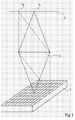
- FIG. 1 schematically represents an image sensor consisting of a matrix of pixels 1 receiving by an objective 2, the image of a distant object plane 3.
- the image of a point A situated in the middle of the object plane is to form substantially in the middle of the matrix 1.
- the image of a point B situated at the edge of the object plane will form at the edge of the matrix 3.
- FIG. 2 is a sectional view of a substantially central photosensitive cell 6 of an image sensor formed on a substrate 7, for example silicon.
- the photosensitive cell 6 is associated with a portion of the surface of the substrate 7 which, seen from above, generally has the shape of a square or a rectangle.
- the photosensitive cell 6 comprises a photosensitive active zone 8 generally corresponding to a photodiode adapted to store a quantity of electric charges as a function of the light intensity received.
- the substrate 7 is covered with a stack of transparent insulation layers 9, 11, 12, 13 which may be, for example, alternately silicon oxide and silicon nitride.
- the conductive tracks 14 and conductive vias 16 are generally metallic. Examples include aluminum, tungsten, copper and metal alloys. These materials are opaque and possibly reflective.
- a color filter element 17 for example an organic filter, is arranged on the stack of the insulation layers 9, 11, 12, 13 at the level of the photosensitive cell 6.
- the filter elements of color 17 are generally covered with a planarized equalizing layer 18 which defines an exposure face 19 exposed to light.
- a microlensicle 21 is disposed on the equalization layer 18, vis-à-vis the photosensitive zone 8 to focus the light rays towards the photosensitive zone 8.
- the paths of two light rays R1, R2 are schematically represented by way of example for the photosensitive cell 6.
- Conductive tracks 14 and conductive vias 16 are arranged so as not to hinder the passage of light rays.
- the microlens 21 is for example obtained by covering the equalization layer 18 with a resin. The resin is etched to delimit distinct resin blocks, each resin block being formed substantially vis-à-vis a photosensitive area 8.
- each resin block then tends to deform by creep to obtain a convex outer surface 22.
- the maximum thickness of the microlens 21 is about 0.5 microns.
- the photosensitive zone 8 covers only a portion of the surface of the substrate 7 associated with the photosensitive cell 6. Indeed, part of the surface is reserved for addressing and reading devices of the photosensitive zone 8. of clarity, these devices have not been shown in FIG.
- Fig. 3 is a sectional view of a photosensitive cell 6 of an image sensor located at the edge of the pixel array.
- two radii R1 ', R2' are represented. It is observed that the focusing of the rays R 1 'and R 2' is done next to the photosensitive zone 8. Thus, at least part of the light spot provided by the microlens 21 does not fall on the photosensitive zone 8 and the edges of the photosensitive zone 8. image, for the same illumination, appear darker than the center of the image. This results in a loss of peripheral sensitivity due to the shift of the projected image on the peripheral parts of the matrix of photosensitive cells.
- the distance T between the microlens 21 and the photosensitive zone 8 does not generally vary significantly.
- the ratio between the distance T and the lateral dimension d therefore tends to increase.
- the microlens 21 must therefore be less convergent to allow focusing on the photosensitive zone 8.
- the microlens 21 must be thinner, which implies that the resin layer deposited on the equalization layer 18 must be thinner.
- a third limitation of the current manufacturing process results from the presence of conductive tracks 14 and conductive vias 16 which can be obstacles and impede the passage of light rays.
- the object of the present invention is to propose an image sensor constituted by a matrix of photosensitive cells making it possible to focus, for each photosensitive cell, more light on the photosensitive zone of the photosensitive cell than the image sensor described in state of the art.
- Another object of the present invention is to overcome the loss of peripheral sensitivity of an image sensor.
- the present invention provides an image sensor pixel structure comprising a photosensitive area, a stack of isolation layers covering the photosensitive area, and a light focusing device of the pixel to the photosensitive area.
- the focusing device comprises first and second microlenses, the first microlens being disposed between layers of the stack and substantially conjugating the second microlens with the photosensitive area.
- the senor comprises a light exposure face and the second microlens is located on the exposure face.
- the first microlens is made of a first material having a first refractive index
- the layers of the stack adjacent to the first microlens being made of a second material having a second index of refraction less than the first refractive index
- the first microlens is based on silicon nitride between two layers of silicon oxide.
- the first microlens is disposed substantially at one third of the distance between the second microlens and the photosensitive zone.
- the invention also relates to an image sensor comprising a set of pixel structures such as above.
- the optical axis of the first microlens and the optical axis of the second microlens of at least one pixel structure of the entire pixel structure are parallel and offset.
- the shift between the optical axis of the first microlens and the optical axis of the second microlens is increased as one moves away from the center of the image sensor.
- the invention also provides a method of manufacturing an image sensor, comprising the steps of forming a photosensitive area at a substrate; forming a first stack of isolation layers; forming for the photosensitive zone a first microlens; forming a second stack of isolation layers; and forming for the photosensitive area a second microlens such that for the photosensitive area, the corresponding first microlens conjugates the corresponding second microlens with said photosensitive area.
- the step of forming the first microlens comprises the following steps: depositing a layer based on silicon nitride; deposit a layer of resin on the first stack; forming, vertically above each desired position of a first microlens, a resin block having the desired shape of the first microlens; and etch the resin block and the silicon nitride layer to form the first microlens in the silicon nitride layer, the first microlens having the shape of the associated resin block.
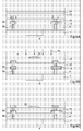
- Figure 4 is a sectional view of an exemplary embodiment of a photosensitive cell 26 of an image sensor.
- the cell 26 has substantially the same structure as the cell 6 of FIG. 2. However, between the isolation layers 11, 12 of the stack of insulation layers 9, 11, 12, 13, the cell photosensitive material 26 comprises a microlens 29.
- a planarized equalization layer 18 covers the filter element 17, the upper face of the layer 18 constitutes the exposure face 19 exposed to the light on which a microlens 27 is arranged.
- the focal length microlens 29 is chosen so that the microlens 29 forms the image of the microlens 27 on the associated photosensitive zone 8.
- the microlens 29 conjugates the plane of the microlens 27 and that of the associated photosensitive zone 8, with a magnification less than or equal to the ratio between the size d of the photosensitive zone and the size of the photosensitive cell 26 ( or microlens 27).
- a focusing device has been formed for focusing the light towards the photosensitive zone 8.
- the optical axis of the microlens 29 is substantially coincident with that of the microlens 27.
- the exemplary R3 and R4 rays converge on the microlens 29. the microlens 29, unlike the rays R1 and R2, which themselves converged directly on the photosensitive zone 8.
- the microlens 27 is therefore more convergent than the microlens 21.
- the outer surface 28 of the microlens 27 is more curved and therefore easier to develop by the standard creep manufacturing process.
- a first advantage of the present invention therefore lies in the implementation of a simpler, more reliable and therefore more repeatable microlensing method 27.
- Figure 5 is a sectional view of a photosensitive cell 26 located at the pixel matrix edge.
- Light rays R3 'and R4' have been shown by way of example.
- the microlens 29 conjugating the microlens 27 with the photosensitive zone 8, the rays R3 'and R4' converge on the microlens 29.
- the image is then reconstituted on the photosensitive zone 8 without loss of luminous intensity or resolution although the structure pixel is at the edge of the matrix.
- a second advantage of the present invention is therefore an improvement in the peripheral sensitivity during the restitution of the image on the photosensitive zone 8 resulting from an automatic refocusing of the image of a peripheral zone.
- FIGS. 6A, 6B and 6C show a photosensitive cell according to the invention at different stages of an exemplary method of manufacturing an image sensor according to the invention.
- Figure 6A illustrates the result of first steps of manufacturing a pixel structure.
- the photosensitive zones 8 are formed by ion implantation of P type dopants.
- An isolation layer 9 is then deposited in which conductive vias 16 are formed.
- conductive tracks 14 are produced before depositing a second insulating layer 11.
- the same procedure as above is followed for the production of conductive vias 16 and conductive tracks 14 associated with isolation layer 11 before re-depositing an insulation layer 12.
- the insulation layer 12 is for example made of silicon nitride whereas the insulation layer 11 is for example made of silicon oxide.
- a layer of resin 32 is then deposited.
- FIG. 6B illustrates a curved structure 33 obtained after etching the resin layer 32 and creeping the etched resin blocks.
- the next step is a step of uniform etching in the direction of the arrows 34.
- the curved resin structure 33 and the insulation layer 12 are etched uniform and selective with respect to the insulation layer 9 and the conductive tracks 14 by plasma etching.
- the shape of the curved structure 33 is reproduced at the level of the layer 11. Such a step is called shape transfer.
- FIG. 6C shows the structure obtained at the end of the shape transfer step which results in the shape of microlens 29.
- the present invention is susceptible of various variations and modifications which will be apparent to those skilled in the art.
- the devices presented in the exemplary embodiments have been for devices comprising two levels of conductive tracks 14 and two levels of conductive vias 16. These devices can be made with a number of levels of conducting tracks 14 and levels. of conductive vias 16 lower or higher.
- the position of the microlens 29 may vary and therefore not necessarily be above the second level of conductive vias 16. In fact the microlens 29 may be performed in a lower or higher level.
- the microlens 29 may be based on silicon nitride and be in a SiNO type compound.
Abstract
Description
La présente invention concerne un capteur d'image comprenant une matrice de cellules photosensibles disposées en lignes et en colonnes et réalisées dans une technologie de type CMOS.The present invention relates to an image sensor comprising a matrix of photosensitive cells arranged in rows and columns and made in a CMOS technology.
La figure 1 représente schématiquement un capteur d'image constitué d'une matrice de pixels 1 recevant par un objectif 2, l'image d'un plan objet éloigné 3. L'image d'un point A situé au milieu du plan objet va se former sensiblement au milieu de la matrice 1. L'image d'un point B situé au bord du plan objet va se former au bord de la matrice 3.FIG. 1 schematically represents an image sensor consisting of a matrix of
La figure 2 est une vue en coupe d'une cellule photosensible 6 sensiblement centrale d'un capteur d'image formée sur un substrat 7 par exemple du silicium. La cellule photosensible 6 est associée à une portion de la surface du substrat 7 qui, vue de dessus, a généralement la forme d'un carré ou d'un rectangle. La cellule photosensible 6 comprend une zone active photosensible 8 correspondant généralement à une photodiode adaptée à stocker une quantité de charges électriques en fonction de l'intensité lumineuse reçue. Le substrat 7 est recouvert d'un empilement de couches d'isolement transparentes 9, 11, 12, 13 qui peuvent être, à titre d'exemple, alternativement de l'oxyde de silicium et du nitrure de silicium. Des pistes conductrices 14, formées entre des couches isolantes adjacentes et des vias conducteurs 16, formés entre deux pistes conductrices, permettent notamment d'adresser la zone photosensible 8 et de recueillir des signaux électriques fournis par la zone photosensible 8. Les pistes conductrices 14 et les vias conducteurs 16 sont généralement métalliques. A titre d'exemple, on peut citer l'aluminium, le tungstène, le cuivre et des alliages métalliques. Ces matériaux sont opaques et éventuellement réfléchissants. Dans un capteur couleur, un élément de filtre de couleur 17, par exemple un filtre organique, est disposé sur l'empilement des couches d'isolement 9, 11, 12, 13 au niveau de la cellule photosensible 6. Les éléments de filtre de couleur 17 sont généralement recouverts d'une couche d'égalisation 18 planarisée qui définit une face d'exposition 19 exposée à la lumière.FIG. 2 is a sectional view of a substantially central
Le maximum de lumière envoyée par l'objectif 2 (figure 1) sur la partie de la face d'exposition 19 associée à la cellule photosensible 1 doit être dirigé vers la zone active photosensible 8. Pour ce faire, une microlentille 21 est disposée sur la couche d'égalisation 18, en vis-à-vis de la zone photosensible 8 pour focaliser les rayons lumineux vers la zone photosensible 8. Les parcours de deux rayons lumineux R1, R2 sont schématiquement représentés à titre d'exemple pour la cellule photosensible 6. Les pistes conductrices 14 et les vias conducteurs 16 sont disposés de façon à ne pas gêner le passage des rayons lumineux. La microlentille 21 est par exemple obtenue en recouvrant la couche d'égalisation 18 d'une résine. La résine est gravée pour délimiter des blocs de résine distincts, chaque bloc de résine étant formé sensiblement en vis-à-vis d'une zone photosensible 8. Les blocs de résine sont ensuite chauffés. Chaque bloc de résine tend alors à se déformer par fluage pour obtenir une surface extérieure convexe 22. A titre d'exemple, pour une cellule photosensible 6 de 4 µm de côté et pour une distance de l'ordre de 8 à 10 µm entre une microlentille 21 et la zone photosensible 8 associée, l'épaisseur maximale de la microlentille 21 est d'environ 0,5 µm.The maximum of light sent by the objective 2 (FIG. 1) on the part of the
La zone photosensible 8 ne couvre qu'une partie de la surface du substrat 7 associée à la cellule photosensible 6. En effet, une partie de la surface est réservée à des dispositifs d'adressage et de lecture de la zone photosensible 8. Par souci de clarté, ces dispositifs n'ont pas été représentés sur la figure 2.The
La figure 3 est une vue en coupe d'une cellule photosensible 6 d'un capteur d'image située au bord de la matrice de pixels. On a représenté à titre d'exemple deux rayons R1', R2'. On observe que la focalisation des rayons R1' et R2' se fait à côté de la zone photosensible 8. Ainsi, au moins une partie de la tache lumineuse fournie par la microlentille 21 ne tombe pas sur la zone photosensible 8 et les bords d'image paraîtront, pour un même éclairement, plus sombres que le centre de l'image. Il en résulte une perte de sensibilité périphérique due au décalage de l'image projetée sur les parties périphériques de la matrice de cellules photosensibles.Fig. 3 is a sectional view of a
On cherche constamment à réduire les dimensions des capteurs d'image afin de pouvoir en intégrer un nombre toujours croissant sur une même surface d'un substrat. Il en résulte, pour la cellule photosensible 6, la réduction de la dimension latérale d de la zone photosensible 8. Par contre, la distance T entre la microlentille 21 et la zone photosensible 8 ne varie généralement pas de manière significative. Le rapport entre la distance T et la dimension latérale d tend donc à augmenter. La microlentille 21 doit donc être moins convergente pour permettre une focalisation sur la zone photosensible 8. La microlentille 21 doit donc être plus fine, ce qui implique que la couche de résine déposée sur la couche d'égalisation 18 doit être plus fine. Lors de l'étape de fluage des blocs de résine gravés dans la couche de résine, il devient en pratique difficile d'obtenir une microlentille avec une forme lui permettant de faire converger correctement les rayons lumineux. En outre, l'augmentation de ce rapport a tendance à augmenter la taille de la tache lumineuse au niveau de la zone photosensible qui peut alors devenir plus large que la zone photosensible. Cela entraîne une perte de l'intensité lumineuse disponible. Une troisième limitation du procédé de fabrication actuel résulte de la présence des pistes conductrices 14 et des vias conducteurs 16 qui peuvent être des obstacles et gêner le passage des rayons lumineux.It is constantly sought to reduce the dimensions of the image sensors so as to be able to integrate an ever increasing number on the same surface of a substrate. As a result, for the
La présente invention vise à proposer un capteur d'image constitué d'une matrice de cellules photosensibles permettant de focaliser, pour chaque cellule photosensible, davantage de lumière sur la zone photosensible de la cellule photosensible que ne le permet le capteur d'image décrit dans l'état de l'art.The object of the present invention is to propose an image sensor constituted by a matrix of photosensitive cells making it possible to focus, for each photosensitive cell, more light on the photosensitive zone of the photosensitive cell than the image sensor described in state of the art.
Un autre objet de la présente invention est de pallier la perte de sensibilité périphérique d'un capteur d'image.Another object of the present invention is to overcome the loss of peripheral sensitivity of an image sensor.
Pour atteindre ces objets, la présente invention prévoit une structure de pixel de capteur d'image comprenant une zone photosensible, un empilement de couches d'isolement recouvrant la zone photosensible, et un dispositif de focalisation de la lumière du pixel vers la zone photosensible. Le dispositif de focalisation comprend des première et seconde microlentilles, la première microlentille étant disposée entre des couches de l'empilement et conjuguant sensiblement la seconde microlentille avec la zone photosensible.To achieve these objects, the present invention provides an image sensor pixel structure comprising a photosensitive area, a stack of isolation layers covering the photosensitive area, and a light focusing device of the pixel to the photosensitive area. The focusing device comprises first and second microlenses, the first microlens being disposed between layers of the stack and substantially conjugating the second microlens with the photosensitive area.
Selon un mode de réalisation de la présente invention, le capteur comprend une face d'exposition à la lumière et la deuxième microlentille est située sur la face d'exposition.According to an embodiment of the present invention, the sensor comprises a light exposure face and the second microlens is located on the exposure face.
Selon un mode de réalisation de la présente invention, la première microlentille est constituée d'un premier matériau ayant un premier indice de réfraction, les couches de l'empilement adjacentes à la première microlentille étant constituées d'un second matériau ayant un second indice de réfraction inférieur au premier indice de réfraction.According to an embodiment of the present invention, the first microlens is made of a first material having a first refractive index, the layers of the stack adjacent to the first microlens being made of a second material having a second index of refraction less than the first refractive index.
Selon un mode de réalisation de la présente invention, la première microlentille est à base de nitrure de silicium entre deux couches d'oxyde de silicium.According to one embodiment of the present invention, the first microlens is based on silicon nitride between two layers of silicon oxide.
Selon un mode de réalisation de la présente invention, la première microlentille est disposée sensiblement au tiers de la distance entre la deuxième microlentille et la zone photosensible.According to one embodiment of the present invention, the first microlens is disposed substantially at one third of the distance between the second microlens and the photosensitive zone.
L'invention vise aussi un capteur d'image comportant un ensemble de structures de pixels tels que ci-dessus.The invention also relates to an image sensor comprising a set of pixel structures such as above.
Selon un mode de réalisation de la présente invention, l'axe optique de la première microlentille et l'axe optique de la seconde microlentille d'au moins une structure de pixel de l'ensemble de la structure de pixels sont parallèles et décalés.According to one embodiment of the present invention, the optical axis of the first microlens and the optical axis of the second microlens of at least one pixel structure of the entire pixel structure are parallel and offset.
Selon un mode de réalisation de la présente invention, le décalage entre l'axe optique de la première microlentille et l'axe optique de la seconde microlentille augmente lorsque l'on s'éloigne du centre du capteur d'image.According to one embodiment of the present invention, the shift between the optical axis of the first microlens and the optical axis of the second microlens is increased as one moves away from the center of the image sensor.
L'invention vise aussi un procédé de fabrication d'un capteur d'image, comprenant les étapes consistant à former une zone photosensible au niveau d'un substrat ; former un premier empilement de couches d'isolement ; former pour la zone photosensible une première microlentille ; former un second empilement de couches d'isolement ; et former pour la zone photosensible une seconde microlentille de sorte que pour la zone photosensible, la première microlentille correspondante conjugue la seconde microlentille correspondante avec ladite zone photosensible.The invention also provides a method of manufacturing an image sensor, comprising the steps of forming a photosensitive area at a substrate; forming a first stack of isolation layers; forming for the photosensitive zone a first microlens; forming a second stack of isolation layers; and forming for the photosensitive area a second microlens such that for the photosensitive area, the corresponding first microlens conjugates the corresponding second microlens with said photosensitive area.
Selon un mode de réalisation de la présente invention, l'étape de formation de la première microlentille comprend les étapes suivantes : déposer une couche à base de nitrure de silicium ; déposer une couche de résine sur le premier empilement ; former à l'aplomb de chaque position souhaitée d'une première microlentille un bloc de résine ayant la forme souhaitée de la première microlentille ; et graver le bloc de résine et la couche à base de nitrure de silicium pour former la première microlentille dans la couche à base de nitrure de silicium, la première microlentille ayant la forme du bloc de résine associé.According to one embodiment of the present invention, the step of forming the first microlens comprises the following steps: depositing a layer based on silicon nitride; deposit a layer of resin on the first stack; forming, vertically above each desired position of a first microlens, a resin block having the desired shape of the first microlens; and etch the resin block and the silicon nitride layer to form the first microlens in the silicon nitride layer, the first microlens having the shape of the associated resin block.
Ces objets, caractéristiques et avantages, ainsi que d'autres de la présente invention seront exposés en détail dans la description suivante d'exemples de réalisation particuliers faite à titre non-limitatif en relation avec les figures jointes parmi lesquelles :
- la figure 1, précédemment décrite, est une vue en perspective schématique d'un capteur d'image ;
- la figure 2, précédemment décrite, est une vue en coupe schématique d'une cellule photosensible d'un capteur d'image ;
- la figure 3, précédemment décrite, est une vue en coupe schématique d'une cellule photosensible située en bord de matrice de pixels ;
- la figure 4 est une vue en coupe schématique d'une cellule photosensible d'un capteur d'image selon la présente invention ;
- la figure 5 est une vue en coupe schématique d'une cellule photosensible selon la présente invention située en bord de matrice de pixels ; et
- les figures 6A, 6B et 6C illustrent des étapes successives d'un procédé de réalisation d'une cellule selon l'invention.
- Figure 1, previously described, is a schematic perspective view of an image sensor;
- Figure 2, previously described, is a schematic sectional view of a photosensitive cell of an image sensor;
- FIG. 3, previously described, is a schematic cross-sectional view of a photosensitive cell situated at the edge of a matrix of pixels;
- Fig. 4 is a schematic sectional view of a photosensitive cell of an image sensor according to the present invention;
- Figure 5 is a schematic sectional view of a photosensitive cell according to the present invention located on the edge of a matrix of pixels; and
- FIGS. 6A, 6B and 6C illustrate successive steps of a method for producing a cell according to the invention.
Par souci de clarté, de mêmes éléments ont été désignés par de mêmes références aux différentes figures et, de plus, comme cela est habituel dans la représentation des circuits intégrés, les diverses figures ne sont pas tracées à l'échelle.For the sake of clarity, the same elements have been designated by the same references in the various figures and, moreover, as is customary in the representation of the integrated circuits, the various figures are not drawn to scale.
La figure 4 est une vue en coupe d'un exemple de réalisation d'une cellule photosensible 26 d'un capteur d'image. La cellule 26 a sensiblement la même structure que la cellule 6 de la figure 2. Toutefois, entre les couches d'isolement 11, 12 de l'empilement de couches d'isolement 9, 11, 12, 13, la cellule photosensible 26 comprend une microlentille 29. Une couche d'égalisation 18 planarisée recouvre l'élément de filtre 17, la face supérieure de la couche 18 constitue la face d'exposition 19 exposée à la lumière sur laquelle est disposée une microlentille 27. La focale de la microlentille 29 est choisie pour que la microlentille 29 forme l'image de la microlentille 27 sur la zone photosensible 8 associée. En d'autres termes, la microlentille 29 conjugue le plan de la microlentille 27 et celui de la zone photosensible 8 associée, avec un grandissement inférieur ou égal au rapport entre la taille d de la zone photosensible et la taille de la cellule photosensible 26 (ou de la microlentille 27). On a ainsi formé un dispositif de focalisation permettant de focaliser la lumière vers la zone photosensible 8. L'axe optique de la microlentille 29 est sensiblement confondu avec celui de la microlentille 27. Les rayons R3 et R4 représentés à titre d'exemple convergent sur la microlentille 29, contrairement aux rayons R1 et R2 qui, eux, convergeaient directement sur la zone photosensible 8. Pour une même distance T entre la microlentille et la zone photosensible, la microlentille 27 est donc plus convergente que la microlentille 21. La surface extérieure 28 de la microlentille 27 est plus bombée et donc plus facile à élaborer par le procédé de fabrication standard de fluage.Figure 4 is a sectional view of an exemplary embodiment of a
Un premier avantage de la présente invention réside donc dans la mise en oeuvre d'un procédé de réalisation de la microlentille 27 plus simple, plus fiable et donc plus répétable.A first advantage of the present invention therefore lies in the implementation of a simpler, more reliable and therefore more
La figure 5 est une vue en coupe d'une cellule photosensible 26 située en bord de matrice de pixels. Des rayons lumineux R3' et R4' ont été représentés à titre d'exemple. La microlentille 29 conjuguant la microlentille 27 avec la zone photosensible 8, les rayons R3' et R4' convergent sur la microlentille 29. L'image est alors reconstituée sur la zone photosensible 8 sans perte d'intensité lumineuse ni de résolution bien que la structure de pixel se trouve en bord de matrice.Figure 5 is a sectional view of a
Un deuxième avantage de la présente invention est donc une amélioration de la sensibilité périphérique lors de la restitution de l'image sur la zone photosensible 8 résultant d'un recentrage automatique de l'image d'une zone périphérique.A second advantage of the present invention is therefore an improvement in the peripheral sensitivity during the restitution of the image on the
Dans un cas extrême dans lequel il faudrait décaler l'axe optique de la microlentille 29 par rapport à l'axe optique de la microlentille 27, afin d'assurer la formation de l'image sur la zone photosensible 8, on aura simplement à déplacer la microlentille 29. On aura ainsi effectué un rattrapage bien moins coûteux qu'une nouvelle disposition des structures de pixels qui nécessiterait l'utilisation d'un nouveau jeu de masques.In an extreme case in which the optical axis of the
Les figures 6A, 6B et 6C représentent une cellule photosensible selon l'invention à différentes étapes d'un exemple de procédé de fabrication d'un capteur d'image selon l'invention.FIGS. 6A, 6B and 6C show a photosensitive cell according to the invention at different stages of an exemplary method of manufacturing an image sensor according to the invention.
La figure 6A illustre le résultat de premières étapes de fabrication d'une structure de pixels. Dans le cas où le substrat 7 est constitué de silicium dopé de type N, les zones photosensibles 8 sont formées par implantation ionique de dopants de type P. On dépose ensuite une couche d'isolement 9 dans laquelle on forme des vias conducteurs 16. Par la suite, on fabrique des pistes conductrices 14 avant de déposer une deuxième couche d'isolement 11. On procède de même que précédemment pour l'élaboration des vias conducteurs 16 et des pistes conductrices 14 associés à la couche d'isolement 11 avant de redéposer une couche d'isolement 12. La couche d'isolement 12 est par exemple en nitrure de silicium tandis que la couche d'isolement 11 est par exemple en oxyde de silicium. On dépose alors une couche de résine 32.Figure 6A illustrates the result of first steps of manufacturing a pixel structure. In the case where the
La figure 6B illustre une structure bombée 33 obtenue après gravure de la couche de résine 32 et fluage des blocs de résine gravés. L'étape suivante est une étape de gravure uniforme dans le sens des flèches 34. La structure bombée 33 en résine et la couche d'isolement 12 sont gravées de manière uniforme et sélective par rapport à la couche d'isolement 9 et aux pistes conductrices 14 par gravure plasma. La forme de la structure bombée 33 se reproduit au niveau de la couche 11. Une telle étape est appelée transfert de forme.FIG. 6B illustrates a
La figure 6C représente la structure obtenue à la fin de l'étape de transfert de forme qui aboutit à la forme de la microlentille 29.FIG. 6C shows the structure obtained at the end of the shape transfer step which results in the shape of
Bien entendu, la présente invention est susceptible de diverses variantes et modifications qui apparaîtront à l'homme de l'art. En particulier, les dispositifs présentées dans les exemples de réalisation l'ont été pour des dispositifs comportant deux niveaux de pistes conductrices 14 et deux niveaux de vias conducteurs 16. On pourra réaliser ces dispositifs avec un nombre de niveaux de pistes conductrices 14 et de niveaux de vias conducteurs 16 inférieur ou supérieur. La position de la microlentille 29 pourra varier et donc ne pas se trouver forcément au-dessus du deuxième niveau de vias conducteurs 16. En effet la microlentille 29 pourra être réalisée dans un niveau inférieur ou supérieur. La microlentille 29 pourra être à base de nitrure de silicium et être en un composé de type SiNO.Of course, the present invention is susceptible of various variations and modifications which will be apparent to those skilled in the art. In particular, the devices presented in the exemplary embodiments have been for devices comprising two levels of
Claims (10)
Applications Claiming Priority (1)
| Application Number | Priority Date | Filing Date | Title |
|---|---|---|---|
| FR0451847 | 2004-08-13 |
Publications (3)
| Publication Number | Publication Date |
|---|---|
| EP1626442A2 true EP1626442A2 (en) | 2006-02-15 |
| EP1626442A3 EP1626442A3 (en) | 2007-02-28 |
| EP1626442B1 EP1626442B1 (en) | 2011-01-12 |
Family
ID=34947097
Family Applications (1)
| Application Number | Title | Priority Date | Filing Date |
|---|---|---|---|
| EP05107383A Active EP1626442B1 (en) | 2004-08-13 | 2005-08-11 | Image sensor |
Country Status (4)
| Country | Link |
|---|---|
| US (1) | US7291826B2 (en) |
| EP (1) | EP1626442B1 (en) |
| JP (1) | JP2006054469A (en) |
| DE (1) | DE602005025834D1 (en) |
Cited By (1)
| Publication number | Priority date | Publication date | Assignee | Title |
|---|---|---|---|---|
| US7208783B2 (en) | 2004-11-09 | 2007-04-24 | Micron Technology, Inc. | Optical enhancement of integrated circuit photodetectors |
Families Citing this family (14)
| Publication number | Priority date | Publication date | Assignee | Title |
|---|---|---|---|---|
| US20060193356A1 (en) * | 2005-01-18 | 2006-08-31 | Robert Osiander | Die level optical transduction systems |
| KR101294470B1 (en) * | 2005-07-08 | 2013-08-07 | 가부시키가이샤 니콘 | Solid-state imaging element |
| US7544982B2 (en) * | 2006-10-03 | 2009-06-09 | Taiwan Semiconductor Manufacturing Company, Ltd. | Image sensor device suitable for use with logic-embedded CIS chips and methods for making the same |
| JP5157436B2 (en) * | 2007-10-11 | 2013-03-06 | 株式会社ニコン | Solid-state imaging device and imaging apparatus |
| US7978255B2 (en) * | 2007-10-11 | 2011-07-12 | Nikon Corporation | Solid-state image sensor and image-capturing device |
| KR100896876B1 (en) * | 2007-11-16 | 2009-05-12 | 주식회사 동부하이텍 | Image sensor and method for manufacturing thereof |
| US8183510B2 (en) * | 2008-02-12 | 2012-05-22 | Omnivision Technologies, Inc. | Image sensor with buried self aligned focusing element |
| US7589306B2 (en) * | 2008-02-12 | 2009-09-15 | Omnivision Technologies, Inc. | Image sensor with buried self aligned focusing element |
| JP2011100900A (en) | 2009-11-06 | 2011-05-19 | Sony Corp | Solid-state imaging apparatus and method of manufacturing and method of designing the same, and electronic apparatus |
| US8981510B2 (en) * | 2010-06-04 | 2015-03-17 | Taiwan Semiconductor Manufacturing Company, Ltd. | Ridge structure for back side illuminated image sensor |
| KR20220150439A (en) | 2012-11-08 | 2022-11-10 | 가부시키가이샤 한도오따이 에네루기 켄큐쇼 | Display device |
| FR3018954B1 (en) * | 2014-03-20 | 2017-07-21 | Commissariat Energie Atomique | METHOD OF OPTIMIZING THE QUANTUM PERFORMANCE OF A PHOTODIODE |
| KR102472276B1 (en) | 2016-03-24 | 2022-11-29 | 에스케이하이닉스 주식회사 | Image sensor |
| CN109411498A (en) * | 2018-10-30 | 2019-03-01 | 德淮半导体有限公司 | Imaging sensor and forming method thereof |
Citations (5)
| Publication number | Priority date | Publication date | Assignee | Title |
|---|---|---|---|---|
| JPH03283572A (en) * | 1990-03-30 | 1991-12-13 | Sony Corp | Solid-state image pick up element |
| JPH1140787A (en) * | 1997-07-15 | 1999-02-12 | Sony Corp | Manufacture of solid-state image pick-up element |
| US6605850B1 (en) * | 1998-03-19 | 2003-08-12 | Canon Kabushiki Kaisha | Solid-state image pickup device using layers having different refractive indices |
| US20030168679A1 (en) * | 2002-02-05 | 2003-09-11 | Junichi Nakai | Semiconductor device and method of manufacturing the same |
| WO2004030101A1 (en) * | 2002-09-27 | 2004-04-08 | Sony Corporation | Solid state imaging device and production method therefor |
Family Cites Families (5)
| Publication number | Priority date | Publication date | Assignee | Title |
|---|---|---|---|---|
| US5739548A (en) * | 1995-05-02 | 1998-04-14 | Matsushita Electronics Corporation | Solid state imaging device having a flattening layer and optical lenses |
| JP3405620B2 (en) * | 1995-05-22 | 2003-05-12 | 松下電器産業株式会社 | Solid-state imaging device |
| JP3620237B2 (en) * | 1997-09-29 | 2005-02-16 | ソニー株式会社 | Solid-state image sensor |
| JP3789365B2 (en) * | 2002-01-31 | 2006-06-21 | シャープ株式会社 | Semiconductor device with in-layer lens and method for manufacturing the same |
| US7372497B2 (en) * | 2004-04-28 | 2008-05-13 | Taiwan Semiconductor Manufacturing Company | Effective method to improve sub-micron color filter sensitivity |
-
2005
- 2005-08-11 EP EP05107383A patent/EP1626442B1/en active Active
- 2005-08-11 DE DE602005025834T patent/DE602005025834D1/en active Active
- 2005-08-12 US US11/202,936 patent/US7291826B2/en active Active
- 2005-08-12 JP JP2005234213A patent/JP2006054469A/en not_active Withdrawn
Patent Citations (5)
| Publication number | Priority date | Publication date | Assignee | Title |
|---|---|---|---|---|
| JPH03283572A (en) * | 1990-03-30 | 1991-12-13 | Sony Corp | Solid-state image pick up element |
| JPH1140787A (en) * | 1997-07-15 | 1999-02-12 | Sony Corp | Manufacture of solid-state image pick-up element |
| US6605850B1 (en) * | 1998-03-19 | 2003-08-12 | Canon Kabushiki Kaisha | Solid-state image pickup device using layers having different refractive indices |
| US20030168679A1 (en) * | 2002-02-05 | 2003-09-11 | Junichi Nakai | Semiconductor device and method of manufacturing the same |
| WO2004030101A1 (en) * | 2002-09-27 | 2004-04-08 | Sony Corporation | Solid state imaging device and production method therefor |
Non-Patent Citations (2)
| Title |
|---|
| PATENT ABSTRACTS OF JAPAN vol. 016, no. 108 (E-1179), 17 mars 1992 (1992-03-17) -& JP 03 283572 A (SONY CORP), 13 décembre 1991 (1991-12-13) * |
| PATENT ABSTRACTS OF JAPAN vol. 1999, no. 05, 31 mai 1999 (1999-05-31) -& JP 11 040787 A (SONY CORP), 12 février 1999 (1999-02-12) * |
Cited By (6)
| Publication number | Priority date | Publication date | Assignee | Title |
|---|---|---|---|---|
| US7208783B2 (en) | 2004-11-09 | 2007-04-24 | Micron Technology, Inc. | Optical enhancement of integrated circuit photodetectors |
| US7459733B2 (en) | 2004-11-09 | 2008-12-02 | Aptina Imaging Corporation | Optical enhancement of integrated circuit photodetectors |
| GB2455224A (en) * | 2004-11-09 | 2009-06-03 | Micron Technology Inc | Integrated circuit photodetector with an embedded microlens |
| GB2420224B (en) * | 2004-11-09 | 2009-09-09 | Agilent Technologies Inc | Integrated circuit photodetectors |
| GB2455224B (en) * | 2004-11-09 | 2009-11-18 | Micron Technology Inc | Integrated circuit photodetetectors |
| US7704780B2 (en) | 2004-11-09 | 2010-04-27 | Aptina Imaging Corporation | Optical enhancement of integrated circuit photodetectors |
Also Published As
| Publication number | Publication date |
|---|---|
| US7291826B2 (en) | 2007-11-06 |
| EP1626442A3 (en) | 2007-02-28 |
| JP2006054469A (en) | 2006-02-23 |
| US20060033008A1 (en) | 2006-02-16 |
| EP1626442B1 (en) | 2011-01-12 |
| DE602005025834D1 (en) | 2011-02-24 |
Similar Documents
| Publication | Publication Date | Title |
|---|---|---|
| EP1626442B1 (en) | Image sensor | |
| EP3667728B1 (en) | Method for manufacturing a device with light-emitting and/or light-receiving diodes and with a self-aligned collimation grid | |
| EP1883112B1 (en) | Back illuminated image sensor with an uniform substrate temperature | |
| EP1793247B1 (en) | Integrated circuit with at least one photocell comprising a multi-level lightguide and corresponding fabrication method | |
| EP1332519B1 (en) | Tft matrix for optical sensor comprising a photosensitive semiconductor layer, and optical sensor comprising such an active matrix | |
| FR2888989A1 (en) | IMAGE SENSOR | |
| EP1870739A1 (en) | Method of manufacturing lenses, in particular for an imager comprising a diaphragm | |
| FR2930840A1 (en) | Contact forming method for lighted image sensing device, involves etching external surface of thin semiconductor substrate, etching insulating region by stopping insulating region on conductive region, and filling etched opening with metal | |
| WO2008007008A2 (en) | Method for producing a matrix of individual electronic components and matrix produced thereby | |
| CN102637707B (en) | Method of producing semiconductor device and method of producing solid-state image pickup device | |
| FR3098988A1 (en) | Image sensor | |
| EP1873836A1 (en) | Back illuminated image sensor | |
| FR2945666A1 (en) | IMAGE SENSOR. | |
| EP3731285B1 (en) | Method for producing a light-emitting and/or light-receiving device with metal optical separation grid | |
| FR2965105A1 (en) | BISPECTRAL MULTILAYER DETECTOR WITH PHOTODIODES | |
| WO2005067054A1 (en) | Method for producing electronic chips consisting of thinned silicon | |
| EP1482558A2 (en) | Photo detector array | |
| FR3010230A1 (en) | PHOTODETECTOR DEVICE WITH SEMICONDUCTOR REGIONS SEPARATED BY A POTENTIAL BARRIER | |
| EP1876647A2 (en) | Back-illuminated image sensor | |
| FR2929478A1 (en) | IMAGE SENSOR WITH IMPROVED SENSITIVITY | |
| EP2157608A1 (en) | Storage of an image in an integrated circuit | |
| FR2862426A1 (en) | CMOS type image sensor, has photosensitive zones provided at level of substrate, and optical head faces that divert light reaching peripheral region of exposed side portion towards each photosensitive zone | |
| FR2928490A1 (en) | INTEGRATED CIRCUIT COMPRISING BURIAL MIRRORS WITH DIFFERENT DEPTHS | |
| FR3102633A1 (en) | Image sensor | |
| EP1870936A1 (en) | Method to produce lenses, particularly for integrated imager |
Legal Events
| Date | Code | Title | Description |
|---|---|---|---|
| PUAI | Public reference made under article 153(3) epc to a published international application that has entered the european phase |
Free format text: ORIGINAL CODE: 0009012 |
|
| AK | Designated contracting states |
Kind code of ref document: A2 Designated state(s): AT BE BG CH CY CZ DE DK EE ES FI FR GB GR HU IE IS IT LI LT LU LV MC NL PL PT RO SE SI SK TR |
|
| AX | Request for extension of the european patent |
Extension state: AL BA HR MK YU |
|
| PUAL | Search report despatched |
Free format text: ORIGINAL CODE: 0009013 |
|
| RIC1 | Information provided on ipc code assigned before grant |
Ipc: H01L 31/0232 20060101ALI20070117BHEP Ipc: H01L 27/146 20060101AFI20070117BHEP |
|
| AK | Designated contracting states |
Kind code of ref document: A3 Designated state(s): AT BE BG CH CY CZ DE DK EE ES FI FR GB GR HU IE IS IT LI LT LU LV MC NL PL PT RO SE SI SK TR |
|
| AX | Request for extension of the european patent |
Extension state: AL BA HR MK YU |
|
| 17P | Request for examination filed |
Effective date: 20070827 |
|
| AKX | Designation fees paid |
Designated state(s): DE FR GB IT |
|
| 17Q | First examination report despatched |
Effective date: 20071004 |
|
| GRAP | Despatch of communication of intention to grant a patent |
Free format text: ORIGINAL CODE: EPIDOSNIGR1 |
|
| GRAS | Grant fee paid |
Free format text: ORIGINAL CODE: EPIDOSNIGR3 |
|
| GRAA | (expected) grant |
Free format text: ORIGINAL CODE: 0009210 |
|
| AK | Designated contracting states |
Kind code of ref document: B1 Designated state(s): DE FR GB IT |
|
| REG | Reference to a national code |
Ref country code: GB Ref legal event code: FG4D Free format text: NOT ENGLISH |
|
| REF | Corresponds to: |
Ref document number: 602005025834 Country of ref document: DE Date of ref document: 20110224 Kind code of ref document: P |
|
| REG | Reference to a national code |
Ref country code: DE Ref legal event code: R096 Ref document number: 602005025834 Country of ref document: DE Effective date: 20110224 |
|
| PLBE | No opposition filed within time limit |
Free format text: ORIGINAL CODE: 0009261 |
|
| STAA | Information on the status of an ep patent application or granted ep patent |
Free format text: STATUS: NO OPPOSITION FILED WITHIN TIME LIMIT |
|
| 26N | No opposition filed |
Effective date: 20111013 |
|
| REG | Reference to a national code |
Ref country code: DE Ref legal event code: R097 Ref document number: 602005025834 Country of ref document: DE Effective date: 20111013 |
|
| REG | Reference to a national code |
Ref country code: FR Ref legal event code: PLFP Year of fee payment: 12 |
|
| REG | Reference to a national code |
Ref country code: FR Ref legal event code: PLFP Year of fee payment: 13 |
|
| REG | Reference to a national code |
Ref country code: FR Ref legal event code: PLFP Year of fee payment: 14 |
|
| PGFP | Annual fee paid to national office [announced via postgrant information from national office to epo] |
Ref country code: GB Payment date: 20200722 Year of fee payment: 16 |
|
| GBPC | Gb: european patent ceased through non-payment of renewal fee |
Effective date: 20210811 |
|
| PG25 | Lapsed in a contracting state [announced via postgrant information from national office to epo] |
Ref country code: GB Free format text: LAPSE BECAUSE OF NON-PAYMENT OF DUE FEES Effective date: 20210811 |
|
| PGFP | Annual fee paid to national office [announced via postgrant information from national office to epo] |
Ref country code: IT Payment date: 20230720 Year of fee payment: 19 |
|
| PGFP | Annual fee paid to national office [announced via postgrant information from national office to epo] |
Ref country code: FR Payment date: 20230720 Year of fee payment: 19 Ref country code: DE Payment date: 20230720 Year of fee payment: 19 |