EP1612870A1 - Method of manufacturing a thermoelectric generator and thermoelectric generator thus obtained - Google Patents
Method of manufacturing a thermoelectric generator and thermoelectric generator thus obtained Download PDFInfo
- Publication number
- EP1612870A1 EP1612870A1 EP04447161A EP04447161A EP1612870A1 EP 1612870 A1 EP1612870 A1 EP 1612870A1 EP 04447161 A EP04447161 A EP 04447161A EP 04447161 A EP04447161 A EP 04447161A EP 1612870 A1 EP1612870 A1 EP 1612870A1
- Authority
- EP
- European Patent Office
- Prior art keywords
- plate
- thermoelectric generator
- thermopile
- teg
- thermocouples
- Prior art date
- Legal status (The legal status is an assumption and is not a legal conclusion. Google has not performed a legal analysis and makes no representation as to the accuracy of the status listed.)
- Withdrawn
Links
Images










Classifications
-
- H—ELECTRICITY
- H10—SEMICONDUCTOR DEVICES; ELECTRIC SOLID-STATE DEVICES NOT OTHERWISE PROVIDED FOR
- H10N—ELECTRIC SOLID-STATE DEVICES NOT OTHERWISE PROVIDED FOR
- H10N10/00—Thermoelectric devices comprising a junction of dissimilar materials, i.e. devices exhibiting Seebeck or Peltier effects
- H10N10/10—Thermoelectric devices comprising a junction of dissimilar materials, i.e. devices exhibiting Seebeck or Peltier effects operating with only the Peltier or Seebeck effects
- H10N10/13—Thermoelectric devices comprising a junction of dissimilar materials, i.e. devices exhibiting Seebeck or Peltier effects operating with only the Peltier or Seebeck effects characterised by the heat-exchanging means at the junction
-
- H—ELECTRICITY
- H10—SEMICONDUCTOR DEVICES; ELECTRIC SOLID-STATE DEVICES NOT OTHERWISE PROVIDED FOR
- H10N—ELECTRIC SOLID-STATE DEVICES NOT OTHERWISE PROVIDED FOR
- H10N10/00—Thermoelectric devices comprising a junction of dissimilar materials, i.e. devices exhibiting Seebeck or Peltier effects
- H10N10/01—Manufacture or treatment
Definitions
- the present invention relates to thermoelectric generators (TEGs) and more specifically to TEGs operated with a heat source having a large thermal resistance.
- the invention also relates to a method of manufacturing TEGs using micro electro mechanical systems (MEMS) and to the positioning of TEGs in case they are used on warm object in a fluid such as air, having a different temperature with respect to its environment, e.g. on a human body or on a body of a warm-blooded animal.
- MEMS micro electro mechanical systems
- thermoelectric generator utilises a temperature difference occurring between a hot (warm) object, i.e. a heat source, and its colder surrounding, i.e. a heat sink, and is used to transform a consequent heat flow into a useful electrical power.
- the necessary heat can be produced by radioactive materials, as e.g. in space applications, or by sources available in the ambient, like e.g. standard cooling/heating systems, pipe lines including pipe lines with warm waste water, surfaces of engines, parts of machines and buildings or by warm-blooded animals or human beings.
- Natural temperature gradients could be used as well as geothermal temperature gradients, temperature gradients on ambient objects when naturally cooling/heating at night/day, temperature differences between a cold river and a warm shore or between a warm river and ice on it, between ice e.g. on water and surrounding air, etc.
- TEGs mounted in a wristwatch have been used to generate electricity from wasted human heat, thus providing a power source for the watch itself, see M. Kishi, H. Nemoto, T. Hamao, M. Yamamoto, S. Sudou, M. Mandai and S. Yamamoto in 'Micro-Thermoelectric Modules and Their Application to Wristwatches as an Energy Source', Proceedings ICT'99 18 th Int. Conference on Thermoelectrics, p.301-307, 1999.
- TEGs can be characterised by an electrical and a thermal resistance and by both voltage and power generated per unit temperature difference between the hot and cold sides of the TEG. The relative importance of these factors depends on the specific application. In general, electrical resistance should be low and, obviously, voltage or power output should be maximised (in particular in applications with small temperature difference, i.e. a few degrees C or few tens degrees C). If a fixed temperature difference is imposed at the boundaries of the TEG, e.g. by means of hot and cold plates, the value of thermal resistance is not crucial.
- the thermal resistance on one hand, has to be large enough to generate a reasonable temperature drop over the device, but on the other hand, has to be small enough to avoid variations in the heat flow.
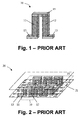
- thermocouple 10 The basic element of a TEG is a thermocouple 10 (Fig. 1).
- An example of a thermocouple 10 for use with the present invention comprises a first leg 11 and a second leg 12 formed of two different thermoelectric materials, for example of the same but opposite doped semiconductor material and exhibiting low thermal conductance and low electrical resistance.
- the legs 11, 12 could be formed from BiTe. If the first leg 11 is formed of n-type BiTe, then the second leg 12 is formed of p-type BiTe, and vice versa.
- the legs 11, 12 are connected by a conductive interconnect, e.g. a metal layer interconnect 13, which forms a low-resistance ohmic contact to the semiconductor legs 11, 12.
- thermopile 21 comprising a plurality of, preferably a large number of thermocouples 10.
- the thermopile 21 is sandwiched between a hot plate 22 and a cold plate 23.
- the hot plate 22 and the cold plate 23 are made of materials having a large thermal conductivity, so that the thermal conductance of the plates 22, 23 is much larger (at least a factor of 10) than the total thermal conductance of the thermopile 21.
- thermoelectric generators the difference between classical and micromachined thermoelectric generators will be discussed.
- the geometrical arrangement of the basic elements or thermocouples 10 composing the TEG 20 may be different, e.g. in-plane position of the thermocouples 10, i.e. parallel to the plates 22, 23, in classical and micromachined TEGs 20, the schemes of Fig. 1 and Fig. 2 hold for both.
- the difference between the two implementations is only quantitative.
- Typical dimensions of legs 11, 12 for a classical TEG 20 are in the order of a few millimeter for the height h and in the order of hundreds of micrometer to 1 millimeter for the square root of the cross-section, which in the further description will be referred to as lateral size a.
- the aspect ratio of the legs 11, 12, which is determined by height h over lateral size a (h/a), may be in the order of 1 to 3 in case of a classical TEG 20.
- the aspect ratio for a state-of-the-art TEG produced by Seiko, i.e. a classical TEG is 7.5.
- the smallest thermopiles 10 available on the market demonstrate an aspect ratio of less than 5.
- the lateral size a is of the order of a few micrometer, and the aspect ratio h/a can be larger than in case of a classical TEG (more than 10).
- the output voltage and power depend on the number of thermocouples 10 comprised in it, and it can easily be shown that the maximum power is obtained when the heat flow through the thermoelectric material is equal to the "parasitic" heat flow through the air, including radiation heat exchange.
- the TEG device area is fixed to 1 cm 2 and the heat flow to 18.5 mW/cm 2 , which is a typical heat flow from a human body skin.
- the legs 11, 12 of the thermocouples 10 are made of resp. n- and p-type BiTe, and that the TEG 20 operates in air.
- the thermal resistance of the metal layer interconnect 13 and the electrical resistance of the contacts between the legs 11, 12 of the thermocouple 10 and the metal layer interconnect 13 are considered to be negligible. Values used for the calculations are reported in Table I. Table I.
- TEG performance Parameters Value Thermal conductivity of BiTe, W K -1 m -1 1.5 Thermal conductivity of air, W K -1 m -1 0.026 Resistivity of BiTe (n and p), ⁇ .m 10 -5 Input heat flow, W m -2 185
- a classical TEG 20 is considered. Dimensions chosen for the legs 11, 12 are close to those of the best commercial devices, i.e. a lateral size a of 250 ⁇ m and a height h of 750 ⁇ m.
- the output power P out (full line) and output voltage V out (dashed line) for such a TEG 20 are illustrated as a function of the number of thermocouples 10.
- the output voltage is low, i.e. 15 mV as can be seen from Fig. 3, which is well below the level necessary for powering standard electronics. Typical voltages are 3 to 5 V. It is easy and efficient and known to a person skilled in the art to up-convert 800 mV to these values, however, it is much more difficult and less efficient to reach these values starting from 300 mV or lower.
- the temperature drop corresponding to the maximum power is about 2.3 K.
- the performance of the TEG 20 can be improved by increasing the aspect ratio of the legs 11, 12.
- the lateral size a and height h of the legs 11, 12 are respectively 80 ⁇ m and 600 ⁇ m.
- a 0.4 cm 2 TEG (10 units of 2x2 mm size are used in the watch) gives a voltage of 0.25 V when it delivers a maximum power of about 20 ⁇ W.
- a micromachined TEG 20 which comprises legs with a thickness of 0.5 ⁇ m, a width of 1 ⁇ m and a height of 5 ⁇ m.
- the output power (#) and voltage ( ⁇ ) are shown as a function of the number of thermocouples 10. The power is limited to only 0.11 ⁇ W. This maximal power is achieved for a TEG 20 comprising about 1.8 million thermocouples 10 (see Fig. 5). For the same number of thermocouples 10, a voltage of about 3V is obtained.
- the temperature difference (#) and the electrical resistance ( ⁇ ) of a micromachined TEG 20 are reported. The temperature difference (#) of the TEG 20 at the maximal power is limited to 18 mK.
- the above results are confirmed by experimental data. For example, as described by M. Strasser, R. Aigner, C. Lauterbach, T.F. Sturm, M. Franosh and G. Wachutka in 'Micromachined CMOS Thermoelectric Generators as On-chip Power Supply', Transducers '03, 12 th International Conference on Solid State Sensors, Actuators and Microsystems, p.45-48, 2003, a large number of thermocouples 10 has been fabricated and a large output voltage is obtained.
- micromachined TEGs produced by Infineon show about 10 mK temperature difference between the hot and the cold side (H. Böttner in 'Thermoelectric Micro Devices: Current State, Recent Developments and future Aspects for Technological Progress and Applications', International Conference on Thermoelectrics, 2002).
- experimental conditions have not been published.
- thermocouples 10 For the number of thermocouples 10 at which the maximum power is achieved (see Fig. 5), the electrical resistance approaches 0.4 G ⁇ (see Fig. 6), which is a too high value for a generator powering electronic devices or battery chargers. It can be seen that the optimal number of thermocouples 10 is about 1.8 million, because in that case the thermal resistance of air is equal to the thermal resistance of thermopile or in series connected thermocouples 10, so the output power is maximized. This large number of thermocouples 10 can be fabricated if one thermocouple 10 occupies a square of only about 7 ⁇ 7 ⁇ m 2 size. This is a difficult but not impossible task.
- thermocouples 10 furthermore has the drawback of increased probability of getting a non-functioning device, since thermocouples 10 are electrically coupled in series. Hence, the failure of one thermocouple 10 will cause the failure of the whole TEG 20. This drawback potentially leads to a dramatically decreased yield of good devices and increased cost of manufacturing.
- P out 1 16 S 2 W u 2 A 2 g te ⁇ 1
- G air 1 16 S 2 W u 2 A g te ⁇ h G a
- ⁇ T W u A 2
- G air W u h 2 g a
- V W u AS 2 g te h a 2 ,
- Equation (1) and (2) show that, at the maximum power condition the number n of necessary thermocouples and the output voltage depends on the ratio h/a 2 , which is much larger for a micromachined TEG than for a classical one. It can then state that micromachined thermoelectric generators require a larger number of thermocouples and deliver power at a larger voltage.
- the power P out and temperature difference ⁇ T depend mainly on the thermal conductance G air of the air between hot plate and the cold plate. Since this thermal conductance G air is large for micromachined thermopiles, the temperature drop ⁇ T and power P out are low for these devices.
- thermoelectric generator TEG wherein the parasitic thermal resistance of air and the height of the legs can be varied and optimised independently. It is furthermore an object of the present invention to provide a method for manufacturing such a TEG.
- thermoelectric generator comprises:
- thermoelectric generator may be characterised by a goodness value, e.g. it may show an output power P out and an output voltage V such that the V.P out product is at least 0.5 ⁇ W.V.
- thermoelectric generator comprising:
- thermocouples comprise two legs having a height h.
- the spacer has a height which is at least ten times larger than the height of the thermocouple legs.
- the first and the second plate may for example be one of a hot and a cold plate.
- thermoelectric generator according to the invention shows a higher density of thermocouples, and thus a reduced number of thermopiles is required for a TEG to be used, for example, for wrist applications.
- thermoelectric generator shows a higher density of thermocouples, and thus a reduced number of thermopiles is required for a TEG to be used, for example, for wrist applications.
- thermopile may be positioned on top of a raised elongate structure, e.g. in the form of a rim or flat topped wall structure.
- a device fabricated according to this preferred embodiment can outperform state of the art devices.
- thermoelectric generator may furthermore comprise a heat-sink or heat-spreading chip/structure in between the thermopile and one of the first plate or the second plate.
- the thermoelectric generator may furthermore comprise a spacer in between the thermopile and one of the first plate or the second plate.
- the parasitic thermal conductance through air between the first plate and the second plate outside the thermopile chip is mainly controlled by the total height of the basic element, and is, as desired, very low, while the parasitic thermal conductance through air between spacers and inside the thermopile and the behaviour of the thermocouple is controlled by the ratios h/a 2 , which preferably is as large as possible unless it decreases the surface density of the thermocouples.
- the second plate may be a cold plate and the thermoelectric generator may comprise a radiator mounted on the cold plate.
- the contact area between the cold plate and air may be increased. By doing so, the heat flow from the body can be improved.
- the radiator may be manufactured in any suitable shape, taking into account its performance, but also its attractive view, cost of manufacturing, different possible applications and related aspects.
- the first plate may have a first size and the second plate may have a second size, the first and second size being different from each other.
- the first plate and the second plate may be unequal size, and thus by matching the heat transfer coefficients of the first plate and second plate, a significant improvement of the generated power and voltage may be achieved.
- the first size or the size of the first plate may be smaller than the second size or the size of the second plate.
- the first plate may be a hot plate and the second plate may be a cold plate, the hot plate being smaller than the cold plate.
- the thermoelectric generator may furthermore comprise a shock-protecting structure and/or a touch protecting structure to protect the thermoelectric generator from external factors, such as for example touching of the thermoelectric generator with e.g. fingers.
- the shock-protecting structure may comprise a thermally isolating plate with pillars from thermally isolating material connected to one of the first plate or the second plate.
- the thermally isolating plate may comprise a hole in which the spacer may be positioned.
- thermoelectric generator may furthermore comprise a thermal screen or shield positioned in between and thermally isolated from both the hot plate and the cold plate.
- the thermoelectric generator may be attached to a device for bring in contact with a wrist, e.g. a watchstrap, or with other body parts of a human or warm blooded animal. This is the case when the thermoelectric generator is, for example, used for wrist applications.
- the thermoelectric generator may then be mounted on a clamp for attaching to a piece of clothing of a human being having a skin, such that one of the first plate or the second plate is in contact with the skin of the human being.
- the clamp may comprise heat isolating paths positioned on the radiator for providing direct contact of the radiator to the piece of clothing.
- thermocouples which form the thermopile may for example comprise SiGe or BiTe couples.
- thermoelectric generator In a second aspect of the invention, a method for the manufacturing of a thermoelectric generator is provided. The method comprises:
- thermocouples comprise two legs having a height, and the height of the spacer may be at least ten times larger than the height of the thermocouples.
- Providing the plurality of thermocouples distributed on the raised elongate structure may comprise etching away areas on the substrate where no thermopiles are positioned. Etching may for example be performed by applying deep reactive ion etching.
- the method may furthermore comprise providing a heat-sink or heat-spreading chip in between the at least one thermopile and one of the first plate or the second plate. This may be done in order to provide a good thermal contact of one side, e.g. the top, of thermocouples to the first or second plate.
- the method may furthermore comprise providing a radiator on top of the cold plate.
- a radiator in the TEG device, the contact area between the cold plate and air may be increased. By doing so, the heat flow from the body can be improved.
- the radiator may be manufactured in any suitable shape, taking into account its performance, but also its attractive view, cost of manufacturing, different possible applications and related aspects.
- the method may furthermore comprise providing a shock-protecting structure and/or a touch-protecting structure to protect the thermoelectric generator from external factors, such as for example touching of the thermoelectric generator with e.g. fingers.
- FOMs Figures Of Merit
- a classical TEG shows good output power (in the order of 15 ⁇ W), but unacceptably low voltage (in the order of 15 mV), while the micromachined state-of-the-art TEG 20 demonstrates good output voltage (in the order of 3 V) but unacceptably low output power (in the order of 0.10 ⁇ W).
- thermopile thermal resistance
- R th,source-sink thermal resistance
- a classical TEG shows a good C T of about 1.3°C if operated on a human body [M. Kishi, H. Nemoto, T. Hamao, M. Yamamoto, S. Sudou, M. Mandai and S. Yamamoto in 'Micro-Thermoelectric Modules and Their Application to Wristwatches as an Energy Source', Proceedings ICT'99 18 th Int. Conference on Thermoelectrics, p.301-307, 1999.], while the micromachined state-of-the-art TEG demonstrates a poor value of C T of only 10 mK [Böttner, A. H. Böttner in 'Thermoelectric Micro Devices: Current State, Recent Developments and future Aspects for Technological Progress and Applications', International Conference on Thermoelectrics, 2002 (ICT2002)]
- the aspect ratio is also an important feature of a TEG.
- the aspect ratio of a classical TEG could be limited in applications where thin TEGs are required, e.g. the ones of 1 mm total thickness including their package.
- the distance in between the hot plate and the cold plate does not limit the aspect ratio, while the thickness of the substrates could be varied. Therefore, it is important to include the capability of the TEG to fit to the minimal thickness requirements of a TEG.
- One of the distinguishing properties of the present invention is that the TEG according to this invention demonstrates significantly large temperature drop on the thermopile per unit height of the legs in case of constant or limited heat flow. So, short legs, i.e.
- FOM 3 V . P out . ⁇ T tp / ( h ( T in - T room ) )
- the V.P out .D.T tp /(h(T in -T room ) product or FOM 3 may be at least 0.5 W.V/m.
- FOM 3 may further be improved by for example increasing the distance between the hot plate and the cold plate.
- Fig. 7a shows a basic element 30 of a thermopile 31 (see Fig. 7b) according to an embodiment of the present invention.
- the basic element 30 comprises two plates 32, 33 which are made of a material with a high thermal conductivity which is at least 10 times higher than the thermal conductivity of the thermocouple 34.
- Suitable materials the plates 32, 33 can be made of are for example Si, Al, AIN, Al 2 O 3 and Cu. However, any other suitable material can be used as well.
- the thickness of the plates 32, 33 which equals in the example given (H-h)/2 wherein H is the total thickness of the basic element 30 and h the height of a thermocouple 34 which is sandwiched in between the two plates 32, 33 (see Fig. 7a), may for example be a few hundred ⁇ m.
- the thermocouple 34 comprises two legs 35, 36 formed out of dissimilar thermoelectric materials.
- the legs 35, 36 may be formed out of the same semiconductor material doped with impurities of an opposite type.
- a first leg 35 may comprise semiconductor material doped with impurities of a first type, e.g.
- n-type impurities such as for example arsenic (As), phosphorus (P), antimony (Sb) or combinations thereof
- a second leg 36 may comprise semiconductor material doped with impurities of a second type, e.g. p-type impurities such as for example boron (B), fluorine (F), nitride (N), indium (In), chlorine (Cl) or combinations thereof, the first and second type of impurities being opposite to each other.
- the legs 35, 36 may for example be formed of BiTe. If leg 35 is made of e.g. n-BiTe (doped with phosphorus), then leg 36 is made of p-BiTe (doped with boron).
- the legs 35, 36 may for example also be formed of SiGe.
- the lateral size b of the plates 32, 33 may for example be in the order of 10-20 times the lateral size of a leg 35, 36 of a thermocouple 34, for example 10 ⁇ m or less.
- the plate size is only limited by the ability of making a thermopile 31 on it. The smaller the lateral size is, the better, until the technology limit is reached.
- the thermocouple 34 in between the plates 32, 33 may have a lateral size a in the order of 1 ⁇ m and a height h in the order of several ⁇ m.
- the thermocouple 34 may be a micromachined thermocouple.
- thermoelectric generator (TEG) 40 thermoelectric generator
- thermopile chip 39 thus comprises a thermopile 31, which is formed by a number of thermocouples 34 connected in series, and two pillars 41a,b, one at each side of the thermocouple 34 and each formed by respective plates 32, 33.
- These pillars 41 a,b will in the further description be referred to as spacers 41a,b as they separate the thermocouples 34 from the hot plate 37 and the cold plate 38.
- the parasitic thermal conductance through air between the hot plate 37 and the cold plate 38 outside the thermopile chip 39 is mainly controlled by the total height H of the basic element 30, and is, as desired, very low, while the parasitic thermal conductance through air between spacers 41 a and 41 b inside the thermopile 39 is controlled by the ratio h/b 2 and the behaviour of the thermocouple 34 is controlled by the ratio h/a 2 , which preferably are as large as possible. Limitation to this value may come from technology and from the maximum space which can be occupied by the device 40. Typical values for a and h may for example be 1 ⁇ m resp. 5 to 20 ⁇ m.
- the TEG 40 as described above is illustrated as comprising a thermopile 31 sandwiched between two spacers 41a,b.
- the TEG 40 as described above is illustrated as comprising a thermopile 31 sandwiched between two spacers 41a,b.
- the TEG 40 as described above is illustrated as comprising a thermopile 31 sandwiched between two spacers 41a,b.
- two spacers 41 a,b only one spacer 41 a or 41 b may be provided, either between the thermopile 31 and the cold plate 38 or between the thermopile 31 and the hot plate 37.
- the size, e.g. the thickness, of the spacers 41a,b may be adapted in order to achieve the best performance for specific applications (see further).
- n G air [ g a b 2 + g tc a 2 h ]
- thermopiles 34 may greatly be reduced, and the maximal power may be increased.
- the expression (11) of the voltage is also similar to expression (4), it mainly depends on the dimensions of the thermocouples 34, i.e. h/a. The output voltage is large, as was desired.
- the maximal power is 15 ⁇ W, which is more than 100 times larger than the maximal power obtainable in prior art micromachined devices (see Fig. 5 and as described by M. Strasser, R. Aigner, C. Lauterbach, T.F. Sturm, M. Franosh and G. Wachutka in 'Micromachined CMOS Thermoelectric Generators as On-chip Power Supply', Transducers '03. 12 th International Conference on Solid State Sensors, Actuators and Microsystems, p.45-48, 2003). However, the performance of the latter if placed on a human body has not been demonstrated.
- the maximal power of 15 ⁇ W is significantly better than the power obtained or estimated for a classical TEG produced by Seiko and as described by M. Kishi, H. Nemoto, T. Hamao, M. Yamamoto, S. Sudou, M. Mandai and S. Yamamoto in 'Micro-Thermoelectric Modules and Their Application to Wristwatches as an Energy Source', Proceedings ICT'99 18 th Int. Conference on Thermoelectrics, p.301-307, 1999.
- thermocouples 34 A prior-art micromachined TEG could be manufactured as shown in Fig.2, and could have a large number of thermocouples 34 if optimised, i.e. feasible. Actually, an in-plane orientation of the thermocouple legs 35, 36 has been used in a TEG produced by Infineon. On a 3.2 x 2.2 mm 2 chip area, 15872 cells are manufactured. One cell of their device represents 2 thermocouples 34 and occupies 49 x 10.9 ⁇ m 2 area, i.e. 49 x 5.45 ⁇ m 2 area per one thermocouple 34 and about 31700 thermocouples 34 per chip, as described by M. Strasser, R. Aigner, C. Lauterbach, T.F. Sturm, M. Franosh and G.
- the calculations give a voltage rise of more than 50 times, 2.3 V / 0.042 V).
- thermocouples compared for (i) a classical TEG, (ii) micromachined TEG and (iii) a TEG according to the present invention is:
- thermopiles 31 For an optimal number of thermopiles 31 at specified conditions (temperature T in inside the body 37°C, environmental temperature T room 20°C, thermal resistance of the body R th 300 cm 2 .K/W, contact area of the device with the skin is 1 cm 2 , and distance between the hot and the cold plates is 1.5 mm), the best FOMs are obtained as illustrated in table II.
- thermopiled TEGs are (1) calculated for a TEG formed by the technology of the present invention except for the thermopiles being positioned on a spacer and (2) are estimated in the case of a chip size not less than 2x2 mm 2 , as it is too difficult to dice and handle/mount/align smaller-size chips. It is not surprising that the maximum occurs at a highest density of the thermocouples and at the minimal die size (again, a 2x2 mm 2 was taken for consideration).
- thermoelectric generator shows a V.P out product of at least 0.5 ⁇ W.V.
- thermopile chip 39 according to the invention comprises a thermopile 31 and at least one spacer 41a,b, either at both sides of the thermopile 31 or between the thermopile 31 and the hot plate 37 or between the thermopile 31 and the cold plate 38.
- the spacer 41a,b may have a height that is at least 10 times larger than the height of the thermocouples 34 forming the thermopile 31.
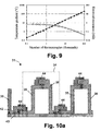
- FIG. 10a cross-sectional view
- Fig. 10b top view
- thermocouples 34 per unit of surface of the spacer 41 a, 41 b must be as large as possible. It is furthermore preferred that the thermocouple legs 35, 36 are normal to the surface 42 of a substrate 43, i.e. in a direction substantially perpendicular to the plane of the substrate 43 (or a bit inclined, if such a requirement comes from the processing). Therefore, in-wafer-plane structures such as thermopiles 34 on a membrane or free-standing in-plane bridges are only the second best choice after the vertical thermocouple legs 35, 36 as shown in Fig. 10a.
- a contact surface 44 between semiconductor material with dopants of a first type, e.g. p-type material (e.g. leg 35), and semiconductor material with dopants of a second type, e.g. n-type material (e.g. leg 36), must be large in order to decrease the contact resistance to negligible values with respect to the thermocouple resistance. This is the major limitation towards a further decrease of the surface occupied by each thermocouple 34.
- Other factors which limit the minimal size of the features are technology, alignment accuracy and topography. The increase of topography limits the resolution (or a minimal feature size), so h/a 2 might not increase.
- thermocouple 34 The lateral size a of the thermocouple 34 must be as small as possible to increase the aspect ratio and, consequently, the thermal resistance R th,tp of thermopile 31 is limited by photolithographic technologies. Accordingly, the height of the thermocouples 34 should be as large as possible, but is technologically limited as well.
- thermoelectric material used to form the legs 35, 36 of the thermocouple 34 such as e.g. SiGe or BiTe, as well as the contact resistance are taken into account
- an optimal area of about 30 ⁇ m 2 may be occupied by each thermocouple 34, if a minimal lithographic feature of 1 ⁇ m is considered.
- the optimal thickness of the legs 35, 36 at a resistivity of 1 m ⁇ .cm and the height of the thermocouples 34 of 5 ⁇ m varies from about 0.5 ⁇ m for BiTe to about 0.3 ⁇ m in case of SiGe.
- thermocouples 34 are in the order of several thousands within the condition that a surface of e.g. 1 cm 2 is in contact with a heat source such as for example a human body and a heat sink such as for example air.
- a heat source such as for example a human body
- a heat sink such as for example air.
- thermopile 31 may occupy a total surface of about 0.1 mm 2 as one thermocouple 34 could occupy, e.g. 30 ⁇ m 2 .
- thermopile chip 39 may be manufactured on a rim 45, as is illustrated in Fig. 11, before it is 'sandwiched' between the hot plate 37 and the cold plate 38 (not shown in Fig. 11).
- the area of the top surface 45a of the rim 45 needs to be kept substantially equal to the total area of thermocouples 34 and must be in the order of 0.1 mm 2 .
- the area of the thermopile chip 39 may be for example in the order of 4 to 20 mm 2 .
- thermocouples 34 Furthermore, in order to provide a good thermal contact of the top of thermocouples 34 to the cold plate 38, a second chip 46, also called a top heat-sink or heat-spreading chip 46, is bonded to the top of the thermocouples 34, for example by reflowing a thin layer of metal (see Fig.11). Mechanically, the micro-thermopiles are very fragile because of the small leg cross-section. A protection is then required during mounting of the heat sink chip 46. To this purpose several thermocouples 34 must not be released so that the presence of the sacrificial layer below makes them robust, and/or supplementary stoppers looking like micro-pillars with the same height as the thermocouples 34 must be manufactured as well on top of the rim 45.
- the maximal power and corresponding voltage, calculated for the structure illustrated in Fig. 11, are resp. 1 ⁇ W and 1 V for a SiGe thermopile, and 6.8 ⁇ W and 2.1 V for a BiTe thermopile.
- thermocouple 34 with a height of 5 ⁇ m occupying an area of 30 ⁇ m 2 is used.
- Micromachined TEG devices produced by Infineon and referred above show an area of 267 ⁇ m 2 per thermocouple 34.
- the thermocouples 34 of the TEGs 40 according to embodiments of the invention thus occupy an area of about 9 times less.
- the above performed calculations show that a device fabricated according to the preferred embodiment of the invention outperforms state of the art devices.
- the above preferred embodiment is given as an example, the dimensions can be varied according to technology improvements and performances can be enhanced.
- thermocouple height becomes less effective beyond 10 to 20 ⁇ m.
- the power increases by 60 %, while further changing the height about 4 times, e.g. from 20 to 80 ⁇ m, gives only 20% increase of the power at the optimized number of thermocouples 34 in the thermopile 31.
- thermocouples 34 in the thermopile 31 plays an important role in obtaining maximal power and voltage from 1 cm 2 surface of a heat source. For example, an increase of the surface occupied by one thermocouple 34 from 5 ⁇ 6 ⁇ m 2 to 20 ⁇ 20 ⁇ m 2 , causes a decrease in the output power by a coefficient of 5.
- thermopile chip 39 In Fig. 12 the preferred configuration of a thermopile chip 39 according to the invention and as illustrated in Fig. 11 is placed in between a hot plate 37 and a cold plate 38. Furthermore, a spacer 41 may be provided in between the thermopile 31, positioned on/under a raised elongate structure or rim 45 in accordance with Fig. 11, and the hot plate 37.
- a further increase of the output power and output voltage can be obtained, e.g. 11.8 ⁇ W resp. 2.1 V in case of BiTe legs 35, 36 and a total spacer height of 5 mm, i.e. the height of the spacer 41 plus 2 chips 45, 46 that serve as a part of the spacer 41 as well.
- the distance between the cold plate 38 and the hot plate 37 may be varied in a wide range.
- thermopile 31 and the cold plate 38 may be provided in between the thermopile 31 and the cold plate 38 (embodiment not represented in the drawings) instead of in between the thermopile 31 and the hot plate 37 or spacers may be provided both in between the thermopile 31 and the hot plate 37 and in between the thermopile 31 and the cold plate 38.
- spacers may be provided both in between the thermopile 31 and the hot plate 37 and in between the thermopile 31 and the cold plate 38.
- the rim 45 may be positioned between the hot plate 37 and the thermopile 31, while the second chip or heat-sink top chip 46 may be positioned between the thermopile 31 and the cold plate 38. Moreover, in another embodiment, the chips 45, 46 may be placed between the hot plate 37 and/or the cold plate 38 and the spacer 41. The functions of the spacer 41 in Fig. 12 may actually be distributed between the spacer 41 itself, the rim 45 and the top heat-sink or heat-spreading chip 46, which serves as a part of spacer 41 as well.
- the FOMs may be improved.
- the performance of a TEG 40 as described in the above embodiment may be enhanced in several ways, e.g. (i) by positioning large-size radiators 48 (see further) on the cold plate 38, like for example radiators 48 used for cooling electronic components, (ii) by increasing the contact area of the TEG 40 with the heat source, (iii) by appropriately choosing materials and design in order to improve thermal isolation between the hot plate 37 and the cold plate 38, (iv) by increasing heat flow or (v) by adapting the TEG 40 to the ambient conditions.
- these possibilities to enhance the performance of the TEG 40 according to embodiments of the invention will be discussed for a TEG 40 attached to a wrist of a person with a watch strap. However, this is only by means of an example and thus is not limiting to the invention.
- the thermal resistance R th,air at the cold plate 38 of the TEG 40 as illustrated in Fig.12 is a few times larger than the thermal resistance occurring inside the human body R th,body . Therefore, by increasing the contact area between the cold plate 38 and air, the heat flow from the body can be improved. Increasing the contact area between the cold plate 38 and air may be done by e.g. increasing the area of the cold plate 38 or by coupling a radiator 48 to the cold plate 38.
- Fig. 13 the cold plate 38 has a larger area with respect to the TEG 40 as illustrate in Fig. 12, while the area of the hot plate 37 is fixed to 1 cm 2 (same area as in Fig. 12). For simplicity, the width of the cold plate 38 has been kept the same and hence, only its length is increased.
- FIG. 13 shows the power ( ⁇ ) and voltage ( ⁇ ) as a function of the area of the cold plate 38 for the device 40 as shown in Fig. 13. Calculations have been performed by assuming that the cold plate 38 of the TEG 40 in Fig. 12 has the same heat transfer coefficient per unit length as the cold plate 38 of the TEG 40 in Fig. 13.
- a significant improvement of the generated power and voltage may be achieved by matching the heat transfer coefficients of the hot plate 37 and cold plate 38, i.e. by making them of unequal size.
- the most rapid change of power and voltage occurs when R th,body ⁇ R th,air .
- the power and voltage strongly depend on the size of the cold plate 38 only if this size is below 10 to 20 cm 2 (see Fig. 14). This is the typical surface occupied by a watch or by a watch and bracelet.
- the air In real conditions of use, the air is not perfectly still, as was assumed in the above considerations, but moves because of different reasons like e.g. air conditioning, natural convection inside buildings, wind outside, and the movement of humans during daytime activity. This brings about a decrease of the optimal ratio of the cold plate area to the area of the hot plate 37, which can be estimated in the range of 1 - 10, depending on particular applications of the device. This means that, for the whole TEG 40, surface dimensions will vary from those of a watch to those of a watch plus bracelet (watch strap).
- a thickness in the order of 1 cm can easily be accepted for a TEG 40, it is possible to mount a radiator 48 onto the cold plate 38 as shown in Fig.15a. This will reduce the surface of the TEG 40.
- Fig.15a a "classical" shape is used for the radiator 48 for simplicity of calculations (see Fig. 15b for a perspective view and details of dimensions of an embodiment).
- the actual shape may also be different, especially for applications on a human body.
- the radiator 48 may be manufactured in any suitable shape, taking into account its performance, but also its attractive view, cost of manufacturing, different possible applications and related aspects.
- Fig. 16a shows the power ( ⁇ ) and voltage ( ⁇ ) as a function of the number n of thermocouples 34 in case of a BiTe thermopile
- Fig. 16b shows the power ( ⁇ ) and voltage ( ⁇ ) as a function of the number n of thermocouples for a SiGe thermopile.
- the height of the spacer 41 is 5 mm and the total thickness of the device is 10.5 mm, i.e. similar to the thickness of a watch.
- Calculations have been performed assuming a contact electrical resistance of 120 ⁇ ⁇ m 2 between the interconnecting metal and the thermoelectric material (e.g.
- BiTe or SiGe with resistivity of 1 m ⁇ .cm, a thermal conductivity of 1.5 W/mK for BiTe and a thermal conductivity of 3 W/m K for SiGe.
- the hot plate area is 1 cm 2 and the heat flow is 18.5 mW/cm 2 . It is noticed that the introduction of the radiator 48 significantly increases the power and the voltage by a factor of about 2.
- radiator 48 further improves the FOMs.
- FOM 1 90 ⁇ W V
- FOM 2 4.9x10 -2 ⁇ m -1
- FOM 3 4.5 V W/m.
- the thermal resistance of the cold plate 38 is made low enough as described above, it may be possible to obtain an even better voltage and power generation by increasing the area of the hot plate 37.
- the total area occupied by the TEG 40 for human body applications is limited.
- the reaction of human beings to the TEG 40 must be taken into account. People easily accept a 1 cm 2 device, which absorbs e.g. 18.5 mW/cm 2 , but often do not accept a 10 cm 2 TEG with the same (or even lower) heat flow per unit surface. This acceptance is related to the physical reaction of their bodies to a local decrease of skin temperature as well as a to a psychological reaction to an unusual (cold) device.
- a second way to improve device performance acting on the hot plate 37 may be performed by structuring a set (pattern) of bumps or miniature needles onto it. These bumps or miniature needles will press or punch the skin partially and locally to decrease (i) the body thermal resistance by decreasing the heat path length in the body, and (ii) the interface thermal resistance by improving local pressure to a skin and increasing the contact surface between the skin and the hot plate 37 at the same size of a hot plate 37.
- thermocouples 34 forming the thermopiles 31, as described in the above embodiments may be distributed in different configurations.
- the thermocouples each have a footprint with a base area, i.e. the area they occupy.
- the thermocouples 31 are distributed on a raised continuous elongate structure over an area of the hot plate 37 (or cold plate 38) whereby the area of the hot plate is substantially larger than the total base area of the thermocouples 31, i.e. the accumulated base area of all thermocouples together.
- Different configurations are illustrated in Fig. 17.
- This figure shows some possibilities for the distribution of thermocouples 31 according to a preferred continuous laterally elongate structure.
- An elongate structure has a length and a width, the length having a dimension which is larger than the dimension of the width.
- the figure is, however, not limiting to the invention, as other continuous elongate structures not represented in the drawings are also possible.
- thermocouples 34 When the thermocouples 34 are distributed between the hot plate 37 and the cold plate 38 as described above, a high thermal current will flow through the thermocouples 34 and thus a high output power of at least 1 ⁇ W may be achieved. Furthermore, by applying the above thermocouple distribution on a laterally elongate structure, and because of the air in between two neighbouring thermocouples 31 positioned in between the hot plate 37 and the cold plate 38, a large temperature drop may be achieved. Hence, a high output voltage of at least 0.5V may be reached.
- thermoelectric generator 40 thus shows a high output voltage V and a high output power P out , and hence shows a high V.P out product of at least 0.5 ⁇ W.V. This is in contrast with the prior art TEG devices, which show either a high output voltage combined with a low output power or a low output voltage combined with a high output power.
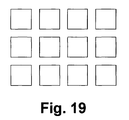
- thermocouples 34 are illustrated in Fig. 18 and 19.
- Fig. 18 shows a discontinuous laterally elongate structure while in Fig. 19 a completely discontinuous distribution is represented.
- Fig. 18 shows a discontinuous laterally elongate structure while in Fig. 19 a completely discontinuous distribution is represented.
- These two possible distribution configurations are less preferred because they show interruptions between neighbouring thermopiles 31. The more interruptions exist between neighbouring thermopiles 31, the more additional connections have to be made to connect the neighbouring thermopiles 31.
- thermoelectric generator 40 with a high output voltage V and a high output power P out , it is clear that the distribution of the thermocouples 34 as described by means of Fig. 18 and 19 are certainly not the most desirable.
- a shock-protecting structure 49 and/or a touch-protecting structure 50 may be important to add to the device.
- the latter is to avoid occasional contact of warm parts of the body with the cold plate 38.
- the structures 49 and 50 may preferably be fabricated from thermal isolator materials such as e.g. plastics. However, suitable metals, semiconductors and natural materials with low thermal conductivity may be used as well.
- a cross section of a TEG 40 comprising a shock-protecting structure 49 is illustrated in Fig. 20.
- the shock-protecting structure 49 may be formed by a thermally isolating plate 51, which may for example be a plastic plate 51, and by pillars 52, which may for example be plastic pillars 52, connecting the thermally isolating plate 51 to the cold plate 38.
- a sidewall made of material with a low thermal conductivity may be used, e.g. for a complete sealing of the TEG 40.
- the thermal conductance of these sidewalls may not significantly affect the thermal properties of the TEG 40.
- Such sidewalls may for example furthermore comprise a set of openings or holes, which are for air convection in the device and to decrease the heat conduction through the sidewalls from the hot plate 37 to the cold plate 38.
- shock-protecting structure 49 may include another type of radiator 48 and is shown in Fig. 21.
- the TEG 40 may furthermore be attached to a watchstrap 53.
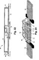
- the shock-protecting structure 49 may be shaped in such a way that it improves heat transfer from the body to the TEG 40, as shown in Fig. 22.
- the thermally isolating plate 51 may comprise a hole 54 in which the spacer 41 with the hot plate 37 may be located or may be going through the hole 54 so that the hot plate 37 would be well below the bottom surface of the thermally isolating plate 51 (as shown in Fig. 22), providing better pressing of the hot plate 37 to the skin and less heat transfer to the thermally isolating plate 51.
- the TEG 40 may furthermore comprise a touch-protecting structure 50.
- the touch-protecting structure 50 may protect the radiator 48 of the TEG device 40 from occasionally being touched by for example fingers.
- a TEG 40 comprising a touch-protecting structure 50 is shown in Fig. 23.
- the touch-protecting structure 50 is preferably not preventing or disturbing to both the air flow and radiation from the hot plate 37. This may be obtained by using a grid-type structure with large openings, as can be seen in Fig. 23.
- the TEG 40 still comprises a shock-protecting structure 49 in the form of a thermally isolating plate 51 and pillars 52 as was illustrated in Figs. 20 and 21.
- the touch-protecting structure 50 may serve simultaneously as a shock-protecting structure.
- the heat isolating supports i.e. the pillars 52 in Fig. 21 and 22, are not necessary anymore if the particular attachment of the radiator 48 to the thermopile assembly properly holds the radiator 48. It is important that the touch-protecting structure 50 does not significantly affect the heat transfer from the radiator 48 to outside of the TEG 40. This may be controlled by providing enough holes in the touch-protecting structure 50, because if the path for heated air is blocked or the output of infrared radiation is prevented, the TEG device 40 will not be effective.
- the performance of the TEG 40 according to the invention may be further improved as a result of improvements related to appropriate choice of materials and design for forming the TEG 40 and of the use in specified circumstances.
- all inner surfaces of the TEG 40 may have low emissivity in the infrared region of the electromagnetic spectrum.
- a number of metals may serve as a low-emissivity materials.
- plastics or other materials used for forming the TEG 40 have large emissivity, they preferably are covered with highly reflecting (low emissivity) material, such as for example a metal.
- highly reflecting (low emissivity) material such as for example a metal.
- the inner volume of the TEG 40 as well as the volume on/in between the chips 45, 46 could be filled with a material showing lower thermal conductivity than the air, e.g. a microporous material.
- a shield or screen 55 may be installed in between and thermally isolated from the hot plate 37 and the cold plate 38. This is illustrated in Fig. 24.
- the parasitic heat coming to the shield or screen 55 has to be dissipated outside the TEG device 40.
- Fig. 25 shows in perspective view the TEG 40 of Fig. 24 attached to a watchstrap 53.
- the cooling part of the screen 55 may be placed above the watchstrap 53;
- Fig. 25 illustrates the screen radiator installed on thermally isolating pillars above the watchstrap.
- the TEG 40 may be protected by a touch-protecting structure 50 and may be isolated from the watchstrap 53 by thermally isolating pillars 52.
- the screen 55 may furthermore comprise a flexible part 56 for bending of the screen radiator, for example when the watchstrap is worn.
- the TEG 40 may furthermore comprise radiating plates 57 on the screen 55 and shock- and touch-protecting structure 58 for the screen 55.
- the TEG 40 may furthermore, for example, comprise a flat radiator 48. However, also other shaped radiators 48 may be used. Instead of the pillars 52, a sheet of a material with low thermal conductivity could be used, possibly provided with holes.
- a screen temperature equal or close to the temperature of the cold plate 38 may be reached, thereby practically eliminating parasitic heat flow from the hot plate 37 to the cold plate 38.
- the shield or screen 55 may canalise the heated air coming from the surrounding skin surface in between the shield 55 and the hot plate 37, protecting the cold plate 38 from parasitic heating by the incoming heated air.
- a first precaution may be to make the outer surfaces of the TEG 401 reflecting to prevent the absorption of sunlight followed by the undesired heating of the cooling surfaces.
- spectrally selective surfaces may be formed with maximal efficiency of radiation of thermal radiation of about 300 K effective blackbody temperature, and reflecting the visible and near-infrared and mid-wave infrared power from the sunlight, including the reflected/scattered one.
- a third precaution may be based on the knowledge that at constant direct sunlight, the temperature of the hot side could exceed the skin temperature. In this case, by making outer surfaces absorb the sunlight, the TEG 40 may be used in reverse mode of operation, i.e. when the heat flow direction is from the radiator to a body, or to another surface, on which the device is mounted. Simple electronic methods exist to rectify such change in polarity of the voltage and obtain the voltage of fixed polarity.
- Fig. 26 shows a cross section of a possible implementation of a TEG 40 according to an embodiment of the invention.
- the TEG 40 may be mounted on a clamp 59 and may then be attached to e.g. a sleeve 60 of clothing that a human body is wearing, such that the hot plate 37 of the TEG 40 is in contact with the wrist of that human body.
- the hot plate 37 is in contact with the skin 61 and is positioned in between the skin 61 and the sleeve 60.
- the principle of the design of the TEG 40 for application on a human body is related to the fact that the sleeve 60, and thus the clothing, is designed such that it decreases the heat dissipation from the body. Therefore, the TEG 40 placed under the clothing, may work worse than in the case of an 'open', not covered, skin 60 / radiator 48 surface. This is important, especially for wrist applications, since in most cases the cloth has sleeves 60 that prevent effective heat dissipation into the air, if the sleeve 60 covers the TEG 40 on a wrist. Therefore, the clamp type device, illustrated in Fig. 26, may be used in this case. Depending on the material properties, e.g.
- the TEG 40 may comprise heat-isolating pads 62 providing direct contact of the radiator 48 to the cloth.
- the latter will serve in this case as an additional radiator.
- the cloth may be layered, and should have low thermal conductance for its inner layers, and high thermal conductance for the outer layers / surface of the cloth.
- metal threads could be included into the cloth material, e.g. cotton, for the outer layer.
- the TEG 40 may furthermore comprise shock-protecting pillars or side walls 63.
- buttons 64 could be made, e.g. on a sleeve 60 (Fig. 27).
- One or more buttons 64 may provide reliable temporary thermal attachment to the TEG 40 while wearing the above cloth.
- the layered cotton described above could be used as well.
- the isolating pads 62 are not required on the outer surface of the cotton, and a good thermal contact must be ensured between the outer surface and the radiator 48.
- Fig. 27 shows a cross section of a device according to an embodiment of the invention, positioned on a wrist with a magnetic clamp 65. The device represents in this case two components.
- the TEG 40 may be attached to the skin 61, for example with a band-aid (not represented in the drawings).
- the separate radiator 48 may be mounted on the cloth.
- the attachment to the cloth e.g. to a sleeve 60, may be provided with small magnets 66 on two plates 67, 68.
- One of the plates, i.e. plate 67, may be connected to a metallic button on the sleeve 60, the other plate, i.e. plate 68 may be on the heat-spreading plate 46 of the TEG 40.
- these plates 67, 68 may be replaced with just a ferromagnetic material.
- the quantity, size and spacing of the buttons 64 on the cloth must guarantee contacting the TEG 40.
- the TEG 40 is suggested as being connected to the skin 61 of a person through the hot plate 37.
- the hot plate 37 and the cold plate 38 may be reversed.
- the TEG 40 may then be configured such that the cold plate 38 is in contact with the skin 61.
- the device surface may be heated and the device may work with the cold plate 38 attached to the skin 61 of a person.
- thermopiles 31 are performed on a planar substrate using deposition (e.g. chemical vapour deposition (CVD) or other suitable deposition techniques), lithography and etching of various layers.
- CVD chemical vapour deposition
- etching of various layers In a second step, deep etching of the substrate is performed in order to fabricate a rim 45. In a last part, the fabrication of the cold plate 38 and its mounting over the thermopile chip 39 is performed.
- thermopiles 31 are formed.
- fabrication details may depend on the thermoelectric material used for forming the thermocouples 34.
- fabrication processes are described for thermopiles 31 comprising SiGe thermocouples and thermopiles 31 comprising BiTe thermocouples.
- SiGe is used as thermoelectric material
- BiTe the process can be easily adapted to SbTe, SbBiTe and similar materials.
- the principle of the fabrication process may be more generally applied to other thermoelectric materials like e.g. skutterudites, nanostructured materials etc.
- the principle of the fabrication process may furthermore be extended to materials with similar chemical properties.
- thermopiles 31 comprising SiGe.
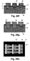
- This fabrication process is illustrated in Fig. 29a to Fig. 291.
- an electrically insulating material 81 is deposited on a thermally conductive substrate 80.
- the substrate 80 may preferably comprise Si, but may also comprise any other suitable thermally conductive material, such as e.g. AIN, Cu, or others, and may have a thickness of between, for example, 600 and 800 ⁇ m.
- the insulating layer may for example comprise SiN.
- the layer of electrically insulating material 81 may have any suitable thickness, depending on the kind of electrically insulating material 81 used and the quality thereof.
- the thickness of the layer of electrically insulating material 81 is preferably chosen such that the material 81 has a compact structure, without pin holes which could produce short circuits.
- a series of trenches 82 are formed. This may e.g. be performed by means of lithographic methods as known by a person skilled in the art.
- the trenches 82 may have a depth d, which should be as deep as possible, e.g. 2.5 ⁇ m, in orderto minimise the parasitic thermal conduction through air.
- the trenches 82 may be as deep as the height of the raised elongate structure or rim 45. This corresponds to the situation where the rim 45 is only present underneath the legs 35, 36 of the thermocouple 34.
- the output power increases by approximately 25% with respect to 2.5 ⁇ m trench. If, in another embodiment, the depth of the trenches 82 is zero, i.e. no trenches 82 are present, the power generated by the TEG 40 may decrease by 20%.
- the trenches 82 may furthermore have a width w 1 which may for example be 8 ⁇ m. As the purpose of the invention is to fabricate a large number of thermopiles 31 in an area as small as possible, w 1 should be as small as possible. However, the limit of w 1 is determined by the lithographic technology. Different layers are used to build onto w 1 (see further in Fig. 291) which have to be aligned to each other.
- w 1 both the number of layers and the tolerances of the lithographic process contribute to the definition of w 1 .
- the size of w 2 may be depend on the same principles. This process is illustrated in Fig. 29a and 29b, which respectively show a cross section and a top view of the structure so far obtained.
- a first layer of insulating sacrificial material 83 which may for example be SiO 2 , is deposited on top of the structure as shown in Fig. 29a and is then planarised. The result is illustrated in Fig. 29c.
- a second layer of the same sacrificial material is deposited and patterned as shown in Fig. 29d (cross section) and Fig. 29e (top view).
- blocks 84 are obtained with a width w 3 , which may for example be 12 ⁇ m.
- the width w 3 may be larger than w 1 so as to allow for alignment errors of photolithographic masks and process accuracy.
- the height of the blocks 84 will be determined by the required height of the spacers 41.
- trenches 82 filled with sacrificial material The purpose of the trenches 82 filled with sacrificial material is to provide a better thermal isolation of the thermocouple 34 without increasing the topography of the surface, as it could adversely affect the photolithographic resolution.
- This step is straightforward in a Si based technology, where planarisation is widely used; it might be more difficult or impossible to implement it in other technologies. In the latter case it can be omitted at the expenses of a reduced (about 20%) output power.
- a thin film of a first thermoelectric material 85 is deposited as shown in Fig. 29f.
- the material can be n- or p-type SiGe and may be deposited by e.g. CVD or by any suitable deposition technique known by a person skilled in the art.
- a thin insulating layer 86 is then deposited and patterned as shown in Fig. 29g.
- the insulating layer 86 may for example be SiO 2 and may have a thickness of e.g. 0.5 ⁇ m.
- the thin film of the first thermoelectric material 85 is then patterned using lithographic methods known by a skilled person.
- Fig. 29h shows the result after patterning of the thin layer of the first thermoelectric material 85.
- thermoelectric material 87 a thin film of a second thermoelectric material 87 is deposited and patterned as shown in Fig. 29i (cross section) and in Fig. 29j (top view).
- the second thermoelectric material may be p- or n-type SiGe deposited by e.g. CVD or by any other suitable deposition technique.
- the second thermoelectric material 87 is that its type (n or p) is opposite to the type of the first thermoelectric material 85. For example, if the first thermoelectric material 85 is n-SiGe, then the second thermoelectric material 87 is p-SiGe.
- a thin film of interconnection material e.g. metal 88 is deposited and patterned as shown in Fig. 29k (cross section) and 291 (top view).
- the thin film of metal 88 may for example comprise aluminium or any other suitable metal.
- BiTe may be deposited by e.g. sputtering or electroplating. If sputtering is chosen, the process may proceed as in above described case of SiGe, except for the fact that a suitable sacrificial material, which can be etched selectively with respect to BiTe must be usedlt is not preferred to use here as a sacrificial layer because the etchant which is used to etch away the parts of the SiO 2 sacrificial layer that are exposed to the etching compound will also etch BiTe. Therefore, in the case of BiTe thermopiles 31, the material used for the sacrificial layer may be any suitable material which can be etched away by an etching compound that does not etch the BiTe material of the thermopiles 31.
- plating is chosen as deposition method, one possibility may be to use the procedure as described by Jeffrey et al. in 'Thermoelectric micro-devices fabricated by a MEMS-like electrochemical process'; Nature Materials, 2, p.528-531, August 2003'.
- the contact area and the cross section of the legs 35, 36 of the thermocouple 34 are identical.
- a contact area of the same cross section of the legs is produced.
- an aim of the present invention to have very small leg cross-sections and low contact resistance. Scaling the above described process to the dimensions recommended for this invention will then give a too large contact resistance.
- the present invention proposes therefore the following process sequence, which is illustrated in Fig. 30a to Fig. 30j.
- the thermally conducting substrate 90 may be any suitable substrate and may for example be AlN, Si or others.
- the electrically insulating layer 91 may have any suitable thickness depending on the kind of electrically insulating material used and the quality thereof. Furthermore, the thickness is preferably chosen such that the material 81 has a compact structure, without pin holes which could produce short circuits.
- a sacrificial resist 92 is then deposited and patterned as illustrated in Fig. 30b. This sacrificial resist 92 may for example comprise ...
- a thin metal film 93 is deposited (see Fig. 30c).
- the thin metal film 93 acts as a seed layer for plating.
- the thin metal film 93 may for example be Cr and may have a thickness of e.g. 5 to 20 nm.
- a first plating resist 94 is deposited, e.g. spinned, in order to define a first plating area (see Fig. 30d). If required for enhancing the electrochemical reactions or for decreasing the contact resistance, a thin film of a metal different from Cr may also be used, such as e.g. Au.
- a first thermoelectric material 95 is then plated at those positions which are not covered by first plating resist 94 (see Fig. 30e).
- the first thermoelectric material 95 may be n- or p-type BiTe or a similar material such as e.g. SbTe or SbBiTe.
- the first plating resist 94 is then removed (Fig.
- a second plating resist 96 is deposited, e.g. spinned, and patterned in order to define a second plating area (Fig. 30g).
- a second thermoelectric material 97 is plated as shown in Fig. 30h, at locations not covered by the second plating resist 96. This material can be p- or n-type BiTe, taken into account that the doping type should be opposite to the doping type of the first thermoelectric material.
- the second plating resist 96 is then removed (Fig. 30i) by suitable techniques known by a person skilled in the art.
- a thin film of interconnection material e.g. metal 98 is deposited and patterned as shown in Fig.30j. This metal may for example be Al or any other suitable metal.
- a next step in the fabrication process of the TEG 40 according to this invention is the fabrication of the rim 45 and the release.
- a thin protective film is deposited onto the substrate 80, 90 comprising the thermopiles 31 as illustrated in cross-section in Fig. 30k and Fig. 30j. It may be convenient, but it is not necessary, to use the same material as the material that has been used for the two sacrificial layers in case of constructing the SiGe thermopiles, e.g. SiO 2 .
- the thin protective film is then patterned in such a way that it protects the fabricated thermopiles 31. The unprotected area is etched away for a depth of a few hundred micrometers.
- the rim 45 may be fabricated by deep reactive ion etching (DRIE). Other etching techniques may also be possible for silicon, as well as for other types of substrates 80, 90. A part of the chip surface could be etched through as well if the remaining area of its surface contacting the hot plate 37 or the cold plate 38 is large enough to ensure low thermal resistance of the substrate-plate interface.
- DRIE deep reactive ion etching
- thermoelectric material to avoid short circuit, the seed layer 93 should be removed by means of a suitable etching technique at those places where it is exposed to the etching compound.
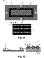
- Fig. 31 top view
- Fig. 32 side view
- thermocouples 34 are not released, i.e. the sacrificial layer remains under the thermocouple 34. They will form a series of robust 'stoppers', whose purpose is to avoid either mechanical stress on the fragile active thermocouples 34, or their destruction during the bonding of the cold plate 38.
- the cold plate 38 can be made by a plain silicon wafer, or by any other material with good thermal conductivity. It can also be shaped in appropriate ways to enhance thermal efficiency. Fabrication and mounting of the cold plate 38 are illustrated in Fig. 33 and 34. In Fig. 33 the cold plate 38 is not yet in contact with the thermopile chip 39, while in Fig. 34 the cold plate 38 is mounted on the thermopile chip 39. An electrically isolating layer 101 is deposited on the substrate, which substrate will later form the cold plate 38. An indium layer is then deposited on that side of the substrate that will be in contact with the thermocouples 34. Besides indium, any other suitable low temperature melting alloy may be used here.
- a two-dimensional pattern 102 (e.g. small squares) is manufactured from the indium layer, for example by photolithography. Pattern dimensions must be small enough to avoid electrical short circuit between neighbouring thermocouples 34, but large enough to provide a good thermal contact with the top aluminum layer of the thermopile chip 39.
- a benzocyclobutylene (BCB) 103 is spinned onto the cold plate 38 and patterned in correspondence with the supports 100 on the thermopile chip 39 in order to form an adhesive layer.
- the cold plate 38 is then flip-chip bonded to the thermopile chip 39 using BCB 103 as an adhesive.
- Curing of BCB 103 is performed e.g. at 150°C, i.e. at a temperature sufficient to reflow indium.
- a heat-sink or heat-spreading chip 46 may furthermore be provided in between the cold plate 37 and the thermopile 31.
- At least one spacer 41 is provided in between the thermopile 31 and at least one of the hot plate 37 or the cold plate 38.
- the method of manufacturing a TEG 40 according to the invention as described above, is not limiting to the invention.
- the rim 45 may also be positioned in between the hot plate 37 and the thermopile 31, while the heat-sink or heat-spreading chip 46 may be positioned in between the cold plate 38 and the thermopile 31.
- thermoelectric materials may be used besides BiTe or SiGe.
Landscapes
- Engineering & Computer Science (AREA)
- Manufacturing & Machinery (AREA)
- Measuring Temperature Or Quantity Of Heat (AREA)
Abstract
Description
- The present invention relates to thermoelectric generators (TEGs) and more specifically to TEGs operated with a heat source having a large thermal resistance. The invention also relates to a method of manufacturing TEGs using micro electro mechanical systems (MEMS) and to the positioning of TEGs in case they are used on warm object in a fluid such as air, having a different temperature with respect to its environment, e.g. on a human body or on a body of a warm-blooded animal.
- A thermoelectric generator (TEG) utilises a temperature difference occurring between a hot (warm) object, i.e. a heat source, and its colder surrounding, i.e. a heat sink, and is used to transform a consequent heat flow into a useful electrical power. The necessary heat can be produced by radioactive materials, as e.g. in space applications, or by sources available in the ambient, like e.g. standard cooling/heating systems, pipe lines including pipe lines with warm waste water, surfaces of engines, parts of machines and buildings or by warm-blooded animals or human beings. Natural temperature gradients could be used as well as geothermal temperature gradients, temperature gradients on ambient objects when naturally cooling/heating at night/day, temperature differences between a cold river and a warm shore or between a warm river and ice on it, between ice e.g. on water and surrounding air, etc.
- There is an increasing interest in miniaturised TEGs, which could replace batteries in consumer electronic products operating at low power. For example, TEGs mounted in a wristwatch have been used to generate electricity from wasted human heat, thus providing a power source for the watch itself, see M. Kishi, H. Nemoto, T. Hamao, M. Yamamoto, S. Sudou, M. Mandai and S. Yamamoto in 'Micro-Thermoelectric Modules and Their Application to Wristwatches as an Energy Source', Proceedings ICT'99 18th Int. Conference on Thermoelectrics, p.301-307, 1999.
- Recently, MEMS technology has also been used to fabricate miniaturised TEGs, as described by M. Strasser, R. Aigner, C. Lauterbach, T.F. Sturm, M. Franosh and G. Wachutka in 'Micromachined CMOS Thermoelectric Generators as On-chip Power Supply', Transducers '03. 12th International Conference on Solid State Sensors, Actuators and Microsystems, p.45-48, 2003; by A. Jacquot, W.L. Liu, G. Chen, J.-P. Fleurial, A. Dausher, B. Lenoir in 'Fabrication and modeling of an in-plane thermoelectric micro-generator', Proceedings ICT '02. 21st International Conference on Thermoelectrics, p.561-564, 2002; and by H. Böttner, A. Schubert, K.H. Schlereth, D. Eberhard, A. Gavrikov, M. Jägle, G. Kühner, C. Künzel, J. Nurnur and G. Plesher in 'New Thermoelectric Components using Micro-System-Technologies', ETS 2001 - 6th European Workshop on Thermoelectrics, 2001.
- TEGs can be characterised by an electrical and a thermal resistance and by both voltage and power generated per unit temperature difference between the hot and cold sides of the TEG. The relative importance of these factors depends on the specific application. In general, electrical resistance should be low and, obviously, voltage or power output should be maximised (in particular in applications with small temperature difference, i.e. a few degrees C or few tens degrees C). If a fixed temperature difference is imposed at the boundaries of the TEG, e.g. by means of hot and cold plates, the value of thermal resistance is not crucial. Contrary thereto, if the boundary condition is a fixed or limited heat flow through the device, then the thermal resistance, on one hand, has to be large enough to generate a reasonable temperature drop over the device, but on the other hand, has to be small enough to avoid variations in the heat flow.
- The basic element of a TEG is a thermocouple 10 (Fig. 1). An example of a
thermocouple 10 for use with the present invention comprises afirst leg 11 and asecond leg 12 formed of two different thermoelectric materials, for example of the same but opposite doped semiconductor material and exhibiting low thermal conductance and low electrical resistance. For example, thelegs first leg 11 is formed of n-type BiTe, then thesecond leg 12 is formed of p-type BiTe, and vice versa. Thelegs semiconductor legs - In Fig. 2, a
TEG 20 comprising athermopile 21 comprising a plurality of, preferably a large number ofthermocouples 10, is shown. Thethermopile 21 is sandwiched between ahot plate 22 and acold plate 23. Thehot plate 22 and thecold plate 23 are made of materials having a large thermal conductivity, so that the thermal conductance of theplates thermopile 21. - Hereinafter, the difference between classical and micromachined thermoelectric generators will be discussed. Although the geometrical arrangement of the basic elements or
thermocouples 10 composing theTEG 20 may be different, e.g. in-plane position of thethermocouples 10, i.e. parallel to theplates micromachined TEGs 20, the schemes of Fig. 1 and Fig. 2 hold for both. The difference between the two implementations is only quantitative. - Typical dimensions of
legs classical TEG 20 are in the order of a few millimeter for the height h and in the order of hundreds of micrometer to 1 millimeter for the square root of the cross-section, which in the further description will be referred to as lateral size a. The aspect ratio of thelegs classical TEG 20. The aspect ratio for a state-of-the-art TEG produced by Seiko, i.e. a classical TEG, is 7.5. Thesmallest thermopiles 10 available on the market (Thermix, Kiev, Ukraine) demonstrate an aspect ratio of less than 5. Formicromachined TEGs 20, the lateral size a is of the order of a few micrometer, and the aspect ratio h/a can be larger than in case of a classical TEG (more than 10). - In case of a constant or limited heat flow through the
TEG 20, the output voltage and power depend on the number ofthermocouples 10 comprised in it, and it can easily be shown that the maximum power is obtained when the heat flow through the thermoelectric material is equal to the "parasitic" heat flow through the air, including radiation heat exchange. - In order to give numerical examples, the TEG device area is fixed to 1 cm2 and the heat flow to 18.5 mW/cm2, which is a typical heat flow from a human body skin. Furthermore, it is assumed that the
legs thermocouples 10 are made of resp. n- and p-type BiTe, and that the TEG 20 operates in air. The thermal resistance of the metal layer interconnect 13 and the electrical resistance of the contacts between thelegs thermocouple 10 and themetal layer interconnect 13 are considered to be negligible. Values used for the calculations are reported in Table I.Table I. Parameters used for the calculation of TEG performance Parameters Value Thermal conductivity of BiTe, W K-1m-1 1.5 Thermal conductivity of air, W K-1 m-1 0.026 Resistivity of BiTe (n and p), Ω.m 10-5 Input heat flow, W m-2 185 - First, a
classical TEG 20 is considered. Dimensions chosen for thelegs TEG 20 are illustrated as a function of the number ofthermocouples 10. In correspondence of the maximum power, the output voltage is low, i.e. 15 mV as can be seen from Fig. 3, which is well below the level necessary for powering standard electronics. Typical voltages are 3 to 5 V. It is easy and efficient and known to a person skilled in the art to up-convert 800 mV to these values, however, it is much more difficult and less efficient to reach these values starting from 300 mV or lower. - As can be seen in Fig. 4, the temperature drop corresponding to the maximum power is about 2.3 K. The performance of the
TEG 20 can be improved by increasing the aspect ratio of thelegs legs thermoelectric legs
technological limit, the voltage obtained is still of impractical use. It can thus be concluded that the low output voltage is the main restriction to a wide use ofstandard TEGs 20 operated in a low heat flow mode. - Next, a
micromachined TEG 20 is considered which comprises legs with a thickness of 0.5 µm, a width of 1 µm and a height of 5 µm. In Fig. 5, the output power (#) and voltage (▲) are shown as a function of the number ofthermocouples 10. The power is limited to only 0.11 µW. This maximal power is achieved for aTEG 20 comprising about 1.8 million thermocouples 10 (see Fig. 5). For the same number ofthermocouples 10, a voltage of about 3V is obtained. In Fig. 6, the temperature difference (#) and the electrical resistance (▲) of amicromachined TEG 20 are reported. The temperature difference (#) of theTEG 20 at the maximal power is limited to 18 mK. The corresponding thermal resistance, which is determined by Rth = ΔT/P (with ΔT= a temperature drop and P the heat flow) is 1 K/W, which is not enough to obtain a good temperature drop. The above results are confirmed by experimental data. For example, as described by M. Strasser, R. Aigner, C. Lauterbach, T.F. Sturm, M. Franosh and G. Wachutka in 'Micromachined CMOS Thermoelectric Generators as On-chip Power Supply', Transducers '03, 12th International Conference on Solid State Sensors, Actuators and Microsystems, p.45-48, 2003, a large number ofthermocouples 10 has been fabricated and a large output voltage is obtained. H. Böttner, A. Schubert, K.H. Schlereth, D. Eberhard, A. Gavrikov, M. Jägle, G. Kühner, C. Künzel, J. Nurnur and G. Plesher point out in 'New Thermoelectric Components using Micro-System-Technologies', ETS 2001 - 6th European Workshop on Thermoelectrics, 2001, that both the temperature drop and the output power are low inmicromachined TEGs 20. For example, micromachined TEGs produced by Infineon show about 10 mK temperature difference between the hot and the cold side (H. Böttner in 'Thermoelectric Micro Devices: Current State, Recent Developments and future Aspects for Technological Progress and Applications', International Conference on Thermoelectrics, 2002). However, experimental conditions have not been published. - For the number of
thermocouples 10 at which the maximum power is achieved (see Fig. 5), the electrical resistance approaches 0.4 GΩ (see Fig. 6), which is a too high value for a generator powering electronic devices or battery chargers. It can be seen that the optimal number ofthermocouples 10 is about 1.8 million, because in that case the thermal resistance of air is equal to the thermal resistance of thermopile or in series connectedthermocouples 10, so the output power is maximized. This large number ofthermocouples 10 can be fabricated if onethermocouple 10 occupies a square of only about 7×7 µm2 size. This is a difficult but not impossible task. The large number ofthermocouples 10 furthermore has the drawback of increased probability of getting a non-functioning device, sincethermocouples 10 are electrically coupled in series. Hence, the failure of onethermocouple 10 will cause the failure of thewhole TEG 20. This drawback potentially leads to a dramatically decreased yield of good devices and increased cost of manufacturing. - In order to understand the difference in behaviour between a classical and a
micromachined TEG 20, a thermal analysis is performed of the TEG configuration as illustrated in Fig. 2. Analytical results are reported and discussed hereinafter. The number of thermocouples n, the temperature drop ΔT and the output voltage Vout at a maximal power Pout are given by the expressions (1) to (4):


- wherein A is the area of the hot/
cold plate - a is the lateral size of the
legs - h is the height of the
legs - ga is the thermal conductivity of air,
- gte is the thermal conductivity of the thermoelectric material the
legs - ρ is the resistivity of the thermoelectric material the
legs - S is the Seebeck coefficient (assumed to be equal for both
legs 11, 12), - Gair is the thermal conductance of the air between the
hot plate 22 and thecold plate 23, - Wu is heat flow per unit area.
- Equation (1) and (2) show that, at the maximum power condition the number n of necessary thermocouples and the output voltage depends on the ratio h/a2, which is much larger for a micromachined TEG than for a classical one. It can then state that micromachined thermoelectric generators require a larger number of thermocouples and deliver power at a larger voltage. The power Pout and temperature difference ΔT (resp. equation (2) and (3)) depend mainly on the thermal conductance Gair of the air between hot plate and the cold plate. Since this thermal conductance Gair is large for micromachined thermopiles, the temperature drop ΔT and power Pout are low for these devices.
- It is an object of the present invention to provide a thermoelectric generator (TEG) wherein the parasitic thermal resistance of air and the height of the legs can be varied and optimised independently. It is furthermore an object of the present invention to provide a method for manufacturing such a TEG.
- The above objectives are accomplished by a method and device according to the present invention.
- In a first aspect of the invention, a thermoelectric generator is provided. The thermoelectric generator comprises:
- at least one thermopile positioned in between a first plate and a second plate, each thermopile comprising a plurality of thermocouples, each thermocouple having a footprint with a base area, and
- at least one spacer for separating the at least one thermopile from at least one of the first plate or the second plate,
- The thermoelectric generator may be characterised by a goodness value, e.g. it may show an output power Pout and an output voltage V such that the V.Pout product is at least 0.5 µW.V.
- The present invention furthermore provides a thermoelectric generator comprising:
- at least one thermopile positioned in between a first plate and a second plate, each thermopile comprising a plurality of thermocouples, each thermocouple having a footprint with a base area,
- at least one spacer for separating the at least one thermopile from at least one of the first plate or the second plate,
- The thermocouples comprise two legs having a height h. According to a preferred embodiment, the spacer has a height which is at least ten times larger than the height of the thermocouple legs.
- The first and the second plate may for example be one of a hot and a cold plate.
- An advantage of the thermoelectric generator according to the invention is that it shows a higher density of thermocouples, and thus a reduced number of thermopiles is required for a TEG to be used, for example, for wrist applications. Hence, by using a drastically reduced number of thermocouples with respect to the prior art micromachined devices, the electrical resistance decreases by a factor of 300 and the yield problems are much less severe.
- In a preferred embodiment of the invention, the thermopile may be positioned on top of a raised elongate structure, e.g. in the form of a rim or flat topped wall structure. A device fabricated according to this preferred embodiment can outperform state of the art devices.
- In order to provide a good thermal contact of the top of the thermocouples to the first or second plate, the thermoelectric generator may furthermore comprise a heat-sink or heat-spreading chip/structure in between the thermopile and one of the first plate or the second plate.
- The thermoelectric generator may furthermore comprise a spacer in between the thermopile and one of the first plate or the second plate. In this arrangement, the parasitic thermal conductance through air between the first plate and the second plate outside the thermopile chip is mainly controlled by the total height of the basic element, and is, as desired, very low, while the parasitic thermal conductance through air between spacers and inside the thermopile and the behaviour of the thermocouple is controlled by the ratios h/a2, which preferably is as large as possible unless it decreases the surface density of the thermocouples.
- In an embodiment of the present invention, the second plate may be a cold plate and the thermoelectric generator may comprise a radiator mounted on the cold plate. By incorporating a radiator in the TEG device, the contact area between the cold plate and air may be increased. By doing so, the heat flow from the body can be improved. The radiator may be manufactured in any suitable shape, taking into account its performance, but also its attractive view, cost of manufacturing, different possible applications and related aspects.
- According to the invention, the first plate may have a first size and the second plate may have a second size, the first and second size being different from each other. By making the first plate and the second plate of unequal size, and thus by matching the heat transfer coefficients of the first plate and second plate, a significant improvement of the generated power and voltage may be achieved. In one embodiment, the first size or the size of the first plate may be smaller than the second size or the size of the second plate. In a specific embodiment of the invention, the first plate may be a hot plate and the second plate may be a cold plate, the hot plate being smaller than the cold plate.
- In particular embodiments of the invention, the thermoelectric generator may furthermore comprise a shock-protecting structure and/or a touch protecting structure to protect the thermoelectric generator from external factors, such as for example touching of the thermoelectric generator with e.g. fingers. The shock-protecting structure may comprise a thermally isolating plate with pillars from thermally isolating material connected to one of the first plate or the second plate. The thermally isolating plate may comprise a hole in which the spacer may be positioned.
- In other embodiments of the invention, the thermoelectric generator may furthermore comprise a thermal screen or shield positioned in between and thermally isolated from both the hot plate and the cold plate. By providing such a thermal screen the parasitic thermal conductance inside the thermoelectric generator between the first plate and the second plate may be minimised.
- In a particular configuration according to an embodiment of the invention, the thermoelectric generator may be attached to a device for bring in contact with a wrist, e.g. a watchstrap, or with other body parts of a human or warm blooded animal. This is the case when the thermoelectric generator is, for example, used for wrist applications. The thermoelectric generator may then be mounted on a clamp for attaching to a piece of clothing of a human being having a skin, such that one of the first plate or the second plate is in contact with the skin of the human being. The clamp may comprise heat isolating paths positioned on the radiator for providing direct contact of the radiator to the piece of clothing.
- According to the present invention, the thermocouples which form the thermopile may for example comprise SiGe or BiTe couples.
- In a second aspect of the invention, a method for the manufacturing of a thermoelectric generator is provided. The method comprises:
- providing at least one thermopile on a substrate, each thermopile comprising a plurality of thermocouples, each thermocouple having a footprint with a base area,
- providing and mounting a first plate and a second plate, and
- providing at least one spacer in between the thermopile and at least one of the first plate or the second plate,
- The thermocouples comprise two legs having a height, and the height of the spacer may be at least ten times larger than the height of the thermocouples.
- Providing the plurality of thermocouples distributed on the raised elongate structure may comprise etching away areas on the substrate where no thermopiles are positioned. Etching may for example be performed by applying deep reactive ion etching.
- According to an embodiment of the invention, the method may furthermore comprise providing a heat-sink or heat-spreading chip in between the at least one thermopile and one of the first plate or the second plate. This may be done in order to provide a good thermal contact of one side, e.g. the top, of thermocouples to the first or second plate.
- When the second plate is a cold plate, the method may furthermore comprise providing a radiator on top of the cold plate. By incorporating a radiator in the TEG device, the contact area between the cold plate and air may be increased. By doing so, the heat flow from the body can be improved. The radiator may be manufactured in any suitable shape, taking into account its performance, but also its attractive view, cost of manufacturing, different possible applications and related aspects.
- In particular embodiments of the invention, the method may furthermore comprise providing a shock-protecting structure and/or a touch-protecting structure to protect the thermoelectric generator from external factors, such as for example touching of the thermoelectric generator with e.g. fingers.
- These and other characteristics, features and advantages of the present invention will become apparent from the following detailed description, taken in conjunction with the accompanying drawings, which illustrate, by way of example, the principles of the invention. This description is given for the sake of example only, without limiting the scope of the invention. The reference figures quoted below refer to the attached drawings.
-
- Fig. 1 is a schematic illustration of a thermocouple comprising an n-type and a p-type semiconducting leg and a metal layer interconnect.
- Fig. 2 is a schematic illustration of a TEG comprising a large number of thermocouples sandwiched between a hot plate and cold plate.
- Fig. 3 shows the voltage (---) and power (―) as a function of the number of thermocouples for a classical BiTe TEG as illustrated in Fig. 2.
- Fig.4 shows the temperature drop as a function of the number of thermocouples for a classical BiTe TEG as illustrated in Fig. 2.
- Fig. 5 shows the voltage (▲) and electrical power (#) transmitted into a matched load for a micromachined BiTe TEG.
- Fig. 6 shows the temperature difference (#) between the hot and cold plates and the electrical resistance (▲) of a micromachined BiTe TEG.
- Fig. 7a is a schematic illustration of a basic element according to an embodiment of the present invention forming a thermopile chip and Fig. 7b is a schematic illustration of a thermopile chip sandwiched between two plates.
- Fig. 8 shows the voltage (▲) and power (#) generated by the thermopile as shown in Fig. 7b.
- Fig. 9 shows the temperature difference (#) between the hot and cold plates and the electrical resistance (▲) of the thermopile chip shown in Fig. 7b.
- Fig. 10a and Fig. 10b are schematic illustrations respectively of a side view and a top view of a thermopile according to a preferred embodiment of the present invention.
- Fig. 11 is a top view (Fig. 11 a) and a side view (Fig. 11 b) of a thermopile chip with the thermopile placed on top of a rim or elongate raised structure, and with a heat-sink top chip in thermal contact with the thermopile chip, according to an embodiment of the present invention.
- Fig. 12 is a side view of the assembly of the thermopile chip with two plates, according to an embodiment of the present invention.
- Fig. 13 is a side view of the assembly of the TEG chips and the pillar with a radiator according to an embodiment of the invention.
- Fig. 14 shows power (#) and voltage (▲) at the optimal number of thermocouples versus the area of the cold plate.
- Fig. 15a is a cross-sectional view of the assembly of a thermopile with a radiator of one embodiment of the invention, and Fig. 15b is an enlarged perspective view of the radiator of Fig. 15a.
- Fig. 16a and Fig. 16b show power (#) and voltage (▲) generated by a 0.5x1x5 µm3 thermopile at a contact resistance of 120 Ω/cm2 for a SiGe thermopile and for a BiTe thermopile respectively.
- Fig. 17 shows some examples of distributed thermopiles in a continuous laterally elongate structure, according to an embodiment of the present invention.
- Fig. 18 shows some examples of distributed thermopiles in a discontinuous laterally elongate structure, according to a further embodiment of the present invention.
- Fig.19 shows some examples of distributed thermopiles in a discontinuous structure, according to yet another embodiment of the present invention.
- Fig. 20 is a cross-sectional view of a TEG according to one embodiment of the invention.
- Fig. 21 is a perspective view of the configuration of Fig. 20 attached to a watchstrap and with a different shape of radiator.
- Fig. 22 is a cross-sectional view of a TEG according to another embodiment of the invention.
- Fig. 23 is a perspective view of the configuration of Fig. 22 attached to a watchstrap.
- Fig. 24 is a cross-sectional view of a TEG according to a further embodiment of the invention.
- Fig. 25 is a perspective view of the configuration of Fig. 24 attached to a watchstrap.
- Fig. 26 is a cross-sectional view of a TEG according to a further embodiment of the present invention mounted on a clamp and attached to a sleeve on a wrist.
- Fig. 27 is a cross-sectional view of a TEG according to yet a further embodiment of the present invention with a magnetic clamp.
- Fig. 28a and Fig. 28b are illustrations of the positioning of a watch and an optimal positioning of a TEG according to the present invention in case of a wrist application, respectively.
- Fig. 29a to Fig. 291 illustrate a fabrication process for SiGe thermopiles according to an embodiment of the present invention.
- Fig. 30a to Fig. 30j illustrate of a fabrication process for BiTe thermopiles according to an embodiment of the invention.
- Fig. 31 is a top view of a TEG mounted on a top plate.
- Fig. 32 is a cross-sectional view of the TEG of Fig. 31.
- Fig. 33 and Fig. 34 illustrate the mounting of the top plate on top of a thermopile chip according to a further embodiment of the present invention.
- In the different figures, the same reference signs refer to the same or analogous elements.
- The present invention will be described with respect to particular embodiments and with reference to certain drawings but the invention is not limited thereto but only by the claims. The drawings described are only schematic and are non-limiting. In the drawings, the size of some of the elements may be exaggerated and not drawn on scale for illustrative purposes. The dimensions and the relative dimensions do not correspond to actual reductions to practice of the invention.
- Furthermore, the terms first, second, third and the like in the description and in the claims, are used for distinguishing between similar elements and not necessarily for describing a sequential or chronological order. It is to be understood that the terms so used are interchangeable under appropriate circumstances and that the embodiments of the invention described herein are capable of operation in other sequences than described or illustrated herein.
- It is to be noticed that the term "comprising", used in the claims, should not be interpreted as being restricted to the means listed thereafter; it does not exclude other elements or steps. Thus, the scope of the expression "a device comprising means A and B" should not be limited to devices consisting only of components A and B. It means that with respect to the present invention, the only relevant components of the device are A and B.
- Hereinafter, 3 parameters called Figures Of Merit (FOMs), are proposed which may be used to illustrate and quantify the advantage of the invention and to compare the proposed device and technology with the state of the art. Hereinafter, FOMs are provided for BiTe TEGs at a resistivity of BiTe of 1 Ω.cm, a thermal conductivity of 15 mW/cm.K, a Seebeck coefficient of 0.2 mV/°C and the following conditions of application on a human body:
- (i) the temperature inside the body, Tin, is 37°C,
- (ii) the environmental temperature Troom is 20°C,
- (iii) still air
- (iv) the thermal resistance of the body Rth is 300 cm2.K/W,
- (v) the contact area of the device with the skin is 1 cm2, and
- (vi) the distance between the first, hot, plate and the second, cold, plate is 1.5 mm without spacer being used, and 5 mm after inserting an additional spacer (see further).
- Since the major advantage of the invention is a large output voltage combined with a large output power, a first FOM may be:

- Under the above proposed conditions a classical TEG shows good output power (in the order of 15 µW), but unacceptably low voltage (in the order of 15 mV), while the micromachined state-of-the-
art TEG 20 demonstrates good output voltage (in the order of 3 V) but unacceptably low output power (in the order of 0.10 µW). - Another important property of the thermal design of a TEG is the ratio of thermal resistance Rth,tp between the hot and cold ends of the thermopile to the thermal resistance Rth,source-sink between the heat source and the sink. This is of lesser importance when the thermopile is used with a constant temperature difference between the hot plate and the cold plate coupled to large heat sinks. However, this becomes important in case of constant or limited heat flow. This ratio is equal to the coefficient of utilization of the temperature difference, CT, occurring between the heat source and the sink. In the above case this coefficient could be defined as:

wherein ΔTtp is the temperature drop over the thermopile. - A classical TEG shows a good CT of about 1.3°C if operated on a human body [M. Kishi, H. Nemoto, T. Hamao, M. Yamamoto, S. Sudou, M. Mandai and S. Yamamoto in 'Micro-Thermoelectric Modules and Their Application to Wristwatches as an Energy Source', Proceedings ICT'99 18th Int. Conference on Thermoelectrics, p.301-307, 1999.], while the micromachined state-of-the-art TEG demonstrates a poor value of CT of only 10 mK [Böttner, A. H. Böttner in 'Thermoelectric Micro Devices: Current State, Recent Developments and future Aspects for Technological Progress and Applications', International Conference on Thermoelectrics, 2002 (ICT2002)]
- Therefore, it is useful to account this coefficient in a Figure of Merit (FOM) for comparison of different technologies.
- The aspect ratio is also an important feature of a TEG. However, the aspect ratio of a classical TEG could be limited in applications where thin TEGs are required, e.g. the ones of 1 mm total thickness including their package. For a micromachined TEG the distance in between the hot plate and the cold plate does not limit the aspect ratio, while the thickness of the substrates could be varied. Therefore, it is important to include the capability of the TEG to fit to the minimal thickness requirements of a TEG. One of the distinguishing properties of the present invention is that the TEG according to this invention demonstrates significantly large temperature drop on the thermopile per unit height of the legs in case of constant or limited heat flow. So, short legs, i.e. few µm, guarantee a large temperature difference obtainable on the thermopile, which is accounted for here together with CT using a second FOM, which is:

- By combining FOM1 and FOM2 as their product, a third FOM may be obtained and used here for comparison with the state of the art. Finally, the third FOM is:

- The principle of the invention is described in Fig. 7a and b. Fig. 7a shows a
basic element 30 of a thermopile 31 (see Fig. 7b) according to an embodiment of the present invention. Thebasic element 30 comprises twoplates thermocouple 34. Suitable materials theplates plates basic element 30 and h the height of athermocouple 34 which is sandwiched in between the twoplates 32, 33 (see Fig. 7a), may for example be a few hundred µm. Thethermocouple 34 comprises twolegs legs first leg 35 may comprise semiconductor material doped with impurities of a first type, e.g. n-type impurities such as for example arsenic (As), phosphorus (P), antimony (Sb) or combinations thereof, and asecond leg 36 may comprise semiconductor material doped with impurities of a second type, e.g. p-type impurities such as for example boron (B), fluorine (F), nitride (N), indium (In), chlorine (Cl) or combinations thereof, the first and second type of impurities being opposite to each other. As an example only, thelegs leg 35 is made of e.g. n-BiTe (doped with phosphorus), thenleg 36 is made of p-BiTe (doped with boron). Alternatively, thelegs - The lateral size b of the
plates leg thermocouple 34, for example 10 µm or less. The plate size is only limited by the ability of making athermopile 31 on it. The smaller the lateral size is, the better, until the technology limit is reached. Thethermocouple 34 in between theplates thermocouple 34 may be a micromachined thermocouple. - An increasing number of the
basic elements 30, as described above, may be inserted in between a first,hot plate 37 and a second,cold plate 38. This is equivalent to inserting a chip with increasing area and comprising an increasing number ofthermocouples 34, as shown in Fig. 7b, in between thehot plate 37 and thecold plate 38, thus forming a thermoelectric generator (TEG) 40. Hereinafter, this chip will be referred to as thethermopile chip 39. - The
thermopile chip 39, according to an embodiment of the invention, thus comprises athermopile 31, which is formed by a number ofthermocouples 34 connected in series, and twopillars 41a,b, one at each side of thethermocouple 34 and each formed byrespective plates pillars 41 a,b will in the further description be referred to asspacers 41a,b as they separate thethermocouples 34 from thehot plate 37 and thecold plate 38. Fig. 7b suggests that in this arrangement the parasitic thermal conductance through air between thehot plate 37 and thecold plate 38 outside thethermopile chip 39 is mainly controlled by the total height H of thebasic element 30, and is, as desired, very low, while the parasitic thermal conductance through air betweenspacers thermopile 39 is controlled by the ratio h/b2 and the behaviour of thethermocouple 34 is controlled by the ratio h/a2, which preferably are as large as possible. Limitation to this value may come from technology and from the maximum space which can be occupied by thedevice 40. Typical values for a and h may for example be 1 µm resp. 5 to 20 µm. - In Fig. 7b, the
TEG 40 as described above is illustrated as comprising athermopile 31 sandwiched between twospacers 41a,b. However, also other configurations are possible according to other embodiments of the present invention. For example, instead of twospacers 41 a,b only onespacer thermopile 31 and thecold plate 38 or between thethermopile 31 and thehot plate 37. Furthermore, the size, e.g. the thickness, of thespacers 41a,b may be adapted in order to achieve the best performance for specific applications (see further). - The performance of the
TEG 40 as illustrated in Fig. 7b may be described by the following formulas:


- For comparing these expressions with the expressions obtained above for a standard micromachined thermopile according to the prior art, it has to be noticed that typically ga is about 100 times less than gte. This means that until b is smaller than 10a, the term gab2 is smaller than gtea2. As a consequence, approximating (gab2 + gtea2) with gtea2 will result in an error of at most a factor of 2. With this in mind, it has to be noticed that expression (9) for the maximal number of
thermocouples 34 and expression (10) for the power are the same as expressions (1) and (2), however, according to the present invention, Gair is now small. As a consequence, the number ofthermopiles 34 to obtain the maximal power may greatly be reduced, and the maximal power may be increased. The expression (11) of the voltage is also similar to expression (4), it mainly depends on the dimensions of thethermocouples 34, i.e. h/a. The output voltage is large, as was desired.
Fig. 8 shows the dependence of power (#) and voltage (▲) on the number ofthermocouples 34 for theTEG 40 illustrated in Fig. 7b. In the calculations, the following values have been used: H = 1.5 mm, b = 5 µm, h = 5 µm and a = 0.7 µm. The maximal power is 15 µW, which is more than 100 times larger than the maximal power obtainable in prior art micromachined devices (see Fig. 5 and as described by M. Strasser, R. Aigner, C. Lauterbach, T.F. Sturm, M. Franosh and G. Wachutka in 'Micromachined CMOS Thermoelectric Generators as On-chip Power Supply', Transducers '03. 12th International Conference on Solid State Sensors, Actuators and Microsystems, p.45-48, 2003). However, the performance of the latter if placed on a human body has not been demonstrated. Furthermore, the maximal power of 15 µW is significantly better than the power obtained or estimated for a classical TEG produced by Seiko and as described by M. Kishi, H. Nemoto, T. Hamao, M. Yamamoto, S. Sudou, M. Mandai and S. Yamamoto in 'Micro-Thermoelectric Modules and Their Application to Wristwatches as an Energy Source', Proceedings ICT'99 18th Int. Conference on Thermoelectrics, p.301-307, 1999. In the latter paper, the watch diameter may be of about 3 cm, so the power of 22.5 µW estimated in the paper, corresponds to about 22.5/(π x 32 /4)=3.2, or approximately 3 µW/cm2 of contact area to the skin. The voltage is 2.3 V, which is only slightly less than the 3V obtained for the prior art micromachined devices, despite the fact that the number ofthermocouples 34 with respect to the prior art micromachined TEG now is significantly decreased. Fig. 9 illustrates the corresponding electrical resistance (▲) and the corresponding temperature difference ΔT (#), which now reaches several °C when the thermocouple number n is small, and which equals 3.3 °C for the optimal value of n = 7000. - A prior-art micromachined TEG could be manufactured as shown in Fig.2, and could have a large number of
thermocouples 34 if optimised, i.e. feasible. Actually, an in-plane orientation of thethermocouple legs thermocouples 34 and occupies 49 x 10.9 µm2 area, i.e. 49 x 5.45 µm2 area per onethermocouple 34 and about 31700thermocouples 34 per chip, as described by M. Strasser, R. Aigner, C. Lauterbach, T.F. Sturm, M. Franosh and G. Wachutka in 'Micromachined CMOS Thermoelectric Generators as On-chip Power Supply', Transducers '03. 12th International Conference on Solid State Sensors, Actuators and Microsystems, p.45-48, 2003. As compared with a classical thermopile (e.g. as Seiko has demonstrated 0.3/(π x 32 /4)=0.042 V/cm2, or approximately 40 µV/cm2), the calculations give a voltage rise of more than 50 times, 2.3 V / 0.042 V). - Hereinafter, the surface density of the thermocouples, compared for (i) a classical TEG, (ii) micromachined TEG and (iii) a TEG according to the present invention is:
- (i) A classical TEG produced by Seiko comprises a 2x2 mm2 chip with 52
thermocouples 34. This is 52/4 mm2 = 13 thermocouples/mm2 and no better results are achieved by any other manufacturer of the classical thermopiles at the same aspect ratio, i.e. h/a=7.5, - (ii) Infineon demonstrated a micromachined TEG with 15872 x 2/(3.2 x 2.2) = 4500 thermocouples/mm2.
- (iii) For embodiments of the present invention, 30 µm2/thermocouple, i.e. a density of 106/30=3x104 mm-2, is achieved, which is a better density than for prior art devices. Since the optimal number of
thermocouples 34 required is less than the number ofthermocouples 34 that can be obtained on 1 mm2 of a chip surface, the present invention only needs a chip surface less than the chip surface required for the prior art devices. - The exemplary results of comparison between classical and
micromachined TEGS 20 on the one hand and theTEG 40 according to the present invention on the other hand are listed in Table II.Table II. Comparative Figures Of Merit for three basic technologies or TEG types. Technology / TEG type Figures Of Merit (FOMs) for a TEG with 1 cm2 area of contact between the TEG and the skin of a human being FOM1 (µW V) FOM2 (µm-1) FOM3 (W V/m) 1. Classical (calculated) 0.4 2x10⁻⁴ 8.3×10⁻⁵ 1. Classical (Seiko watch, estimated) 0.09 1.2x10⁻⁴ 1.1 x10 -52. Micromachined with our chip technology, but no pillars (calculated) 4.6 4x10⁻³ 0.018 2. Micromachined 0.2 6.4x10⁻⁵ 1.3x10⁻⁵ (Infineon, estimated) 3. On a spacer (present invention) 16.7 2.6x10⁻² 0.44 - The values for the "Classical" TEG are obtained by (1) calculating and (2) performing (estimated) calculations for the Seiko approach. Calculations are carried out for a 2x2 mm2 chip size of
Seiko comprising thermocouples 34 with leg dimensions h=600 µm and a=80 µm. For an optimal number ofthermopiles 31 at specified conditions (temperature Tin inside thebody 37°C,environmental temperature T room 20°C, thermal resistance of the body Rth 300 cm2.K/W, contact area of the device with the skin is 1 cm2, and distance between the hot and the cold plates is 1.5 mm), the best FOMs are obtained as illustrated in table II. - Values for "Micromachined" TEGs are (1) calculated for a TEG formed by the technology of the present invention except for the thermopiles being positioned on a spacer and (2) are estimated in the case of a chip size not less than 2x2 mm2, as it is too difficult to dice and handle/mount/align smaller-size chips. It is not surprising that the maximum occurs at a highest density of the thermocouples and at the minimal die size (again, a 2x2 mm2 was taken for consideration).
- The values for a TEG "on a spacer" are obtained for a
TEG 40 according to an embodiment of the present invention as illustrated in Fig. 10 to 12 without additional improvements such as e.g. a radiator and position on the body (see further). - An additional advantage of the TEG configuration according to an embodiment of the present invention is that, by using a drastically reduced number of
thermocouples 34 with respect to the prior art micromachined devices, the electrical resistance decreases by a factor of 300 and the yield problems are much less severe. It is evident that a fabrication method forthermopiles 31 arranged as described above may provide aTEG 40 featuring a large voltage V, i.e. at least a value of 500 mV and a large output power Pout, i.e. at least a value of 1 µW at the same time, which is in contrast with the devices known from the prior art, the same conditions being taken into consideration, i.e. body and related heat flow, still air, room temperature, the same thermocouple material, the same size of thermopile. Hence, the thermoelectric generator according to the present invention, shows a V.Pout product of at least 0.5 µW.V. - A possible configuration of a
thermopile 31 according to an embodiment the invention will be described hereinafter. However, it is to be understood that the invention is not limited to this configuration. As already described above (see Fig. 7b), athermopile chip 39 according to the invention comprises athermopile 31 and at least onespacer 41a,b, either at both sides of thethermopile 31 or between thethermopile 31 and thehot plate 37 or between thethermopile 31 and thecold plate 38. Preferably, thespacer 41a,b may have a height that is at least 10 times larger than the height of thethermocouples 34 forming thethermopile 31. A preferred configuration of athermopile 31 is illustrated in Fig. 10a (cross-sectional view) and Fig. 10b (top view). According to an embodiment of the invention, there are some relevant points of the design that are to be taken into account. The density ofthermocouples 34 per unit of surface of thespacer thermocouple legs surface 42 of asubstrate 43, i.e. in a direction substantially perpendicular to the plane of the substrate 43 (or a bit inclined, if such a requirement comes from the processing). Therefore, in-wafer-plane structures such asthermopiles 34 on a membrane or free-standing in-plane bridges are only the second best choice after thevertical thermocouple legs - A
contact surface 44 between semiconductor material with dopants of a first type, e.g. p-type material (e.g. leg 35), and semiconductor material with dopants of a second type, e.g. n-type material (e.g. leg 36), must be large in order to decrease the contact resistance to negligible values with respect to the thermocouple resistance. This is the major limitation towards a further decrease of the surface occupied by eachthermocouple 34. Other factors which limit the minimal size of the features are technology, alignment accuracy and topography. The increase of topography limits the resolution (or a minimal feature size), so h/a2 might not increase. - The lateral size a of the
thermocouple 34 must be as small as possible to increase the aspect ratio and, consequently, the thermal resistance Rth,tp ofthermopile 31 is limited by photolithographic technologies. Accordingly, the height of thethermocouples 34 should be as large as possible, but is technologically limited as well. - When material properties of the thermoelectric material used to form the
legs thermocouple 34, such as e.g. SiGe or BiTe, as well as the contact resistance are taken into account, an optimal area of about 30 µm2 may be occupied by eachthermocouple 34, if a minimal lithographic feature of 1 µm is considered. The optimal thickness of thelegs thermocouples 34 of 5 µm varies from about 0.5 µm for BiTe to about 0.3 µm in case of SiGe. - When describing the principles of the invention, it has to be noticed that the optimal number of
thermocouples 34 is in the order of several thousands within the condition that a surface of e.g. 1 cm2 is in contact with a heat source such as for example a human body and a heat sink such as for example air. This means that thethermopile 31 may occupy a total surface of about 0.1 mm2 as onethermocouple 34 could occupy, e.g. 30 µm2. - Since it is extremely difficult, or even impossible, to dice and to handle a chip of such small size to align and to assemble it with a heat-sink or heat-spreading chip (see below) placed on top, and to mount the assembly into a
TEG 40, thethermopile chip 39 according to a preferred embodiment of the invention may be manufactured on arim 45, as is illustrated in Fig. 11, before it is 'sandwiched' between thehot plate 37 and the cold plate 38 (not shown in Fig. 11). The area of thetop surface 45a of therim 45 needs to be kept substantially equal to the total area ofthermocouples 34 and must be in the order of 0.1 mm2. The area of thethermopile chip 39 may be for example in the order of 4 to 20 mm2. - Furthermore, in order to provide a good thermal contact of the top of
thermocouples 34 to thecold plate 38, asecond chip 46, also called a top heat-sink or heat-spreadingchip 46, is bonded to the top of thethermocouples 34, for example by reflowing a thin layer of metal (see Fig.11). Mechanically, the micro-thermopiles are very fragile because of the small leg cross-section. A protection is then required during mounting of theheat sink chip 46. To this purposeseveral thermocouples 34 must not be released so that the presence of the sacrificial layer below makes them robust, and/or supplementary stoppers looking like micro-pillars with the same height as thethermocouples 34 must be manufactured as well on top of therim 45. The maximal power and corresponding voltage, calculated for the structure illustrated in Fig. 11, are resp. 1 µW and 1 V for a SiGe thermopile, and 6.8 µW and 2.1 V for a BiTe thermopile. - For the hereinafter performed calculations, a
thermocouple 34 with a height of 5 µm occupying an area of 30 µm2 is used. Micromachined TEG devices produced by Infineon and referred above show an area of 267 µm2 perthermocouple 34. Thethermocouples 34 of theTEGs 40 according to embodiments of the invention thus occupy an area of about 9 times less. Hence, the above performed calculations show that a device fabricated according to the preferred embodiment of the invention outperforms state of the art devices. The above preferred embodiment is given as an example, the dimensions can be varied according to technology improvements and performances can be enhanced. - Hereinafter, the most relevant changes of the TEG performance due to variation in design parameters will be discussed. The effect of increasing the aspect ratio h/a while keeping the same cross-section of the
thermocouple 34, i.e. while keeping "a" constant, and the same chip area perthermocouple 34, which is 30 µm2 in the example given, has been analyzed. It has been found that an increase of the thermocouple height becomes less effective beyond 10 to 20 µm. For example, if the height of thelegs thermocouples 34 in thethermopile 31. - The surface density of
thermocouples 34 in thethermopile 31 plays an important role in obtaining maximal power and voltage from 1 cm2 surface of a heat source. For example, an increase of the surface occupied by onethermocouple 34 from 5×6 µm2 to 20×20 µm2, causes a decrease in the output power by a coefficient of 5. - In Fig. 12 the preferred configuration of a
thermopile chip 39 according to the invention and as illustrated in Fig. 11 is placed in between ahot plate 37 and acold plate 38. Furthermore, aspacer 41 may be provided in between thethermopile 31, positioned on/under a raised elongate structure or rim 45 in accordance with Fig. 11, and thehot plate 37. By changing the features of thespacer 41, for example by making thisspacer 41 higher, i.e. by increasing the distance between thecold plate 38 and thehot plate 37, a further increase of the output power and output voltage can be obtained, e.g. 11.8 µW resp. 2.1 V in case ofBiTe legs spacer 41 plus 2chips spacer 41 as well. According to embodiments of the invention, the distance between thecold plate 38 and thehot plate 37 may be varied in a wide range. - It is to be understood that the TEG configuration as illustrated in Fig. 12 is not limiting to the invention. A spacer may be provided in between the
thermopile 31 and the cold plate 38 (embodiment not represented in the drawings) instead of in between thethermopile 31 and thehot plate 37 or spacers may be provided both in between thethermopile 31 and thehot plate 37 and in between thethermopile 31 and thecold plate 38. It has furthermore to be noted that the position of the raised elongate structure orrim 45, forming the first chip, and the second chip or heat-sink top chip 46 may be reversed, i.e. therim 45 may be positioned between thehot plate 37 and thethermopile 31, while the second chip or heat-sink top chip 46 may be positioned between thethermopile 31 and thecold plate 38. Moreover, in another embodiment, thechips hot plate 37 and/or thecold plate 38 and thespacer 41. The functions of thespacer 41 in Fig. 12 may actually be distributed between thespacer 41 itself, therim 45 and the top heat-sink or heat-spreadingchip 46, which serves as a part ofspacer 41 as well. - By increasing the height of the
spacer 41, the FOMs may be improved. For example, for a spacer height of 5 mm, and the other conditions being the same as described at the start of the description, the FOMs may be: FOM1 = 27 µW V, FOM2 = 3.10-2 µm-1, and FOM3 = 0.8 V W/m. - The performance of a
TEG 40 as described in the above embodiment may be enhanced in several ways, e.g. (i) by positioning large-size radiators 48 (see further) on thecold plate 38, like forexample radiators 48 used for cooling electronic components, (ii) by increasing the contact area of theTEG 40 with the heat source, (iii) by appropriately choosing materials and design in order to improve thermal isolation between thehot plate 37 and thecold plate 38, (iv) by increasing heat flow or (v) by adapting theTEG 40 to the ambient conditions. Hereinafter, these possibilities to enhance the performance of theTEG 40 according to embodiments of the invention will be discussed for aTEG 40 attached to a wrist of a person with a watch strap. However, this is only by means of an example and thus is not limiting to the invention. - At normal temperature and pressure, i.e. at a temperature of about 20°C and a pressure of about 100 kPa, and in still air, the thermal resistance Rth,air at the
cold plate 38 of theTEG 40 as illustrated in Fig.12, is a few times larger than the thermal resistance occurring inside the human body Rth,body. Therefore, by increasing the contact area between thecold plate 38 and air, the heat flow from the body can be improved. Increasing the contact area between thecold plate 38 and air may be done by e.g. increasing the area of thecold plate 38 or by coupling aradiator 48 to thecold plate 38. - In Fig. 13 the
cold plate 38 has a larger area with respect to theTEG 40 as illustrate in Fig. 12, while the area of thehot plate 37 is fixed to 1 cm2 (same area as in Fig. 12). For simplicity, the width of thecold plate 38 has been kept the same and hence, only its length is increased. A schematic illustration of this device is shown in Fig.13. Fig. 14 shows the power (○) and voltage (▲) as a function of the area of thecold plate 38 for thedevice 40 as shown in Fig. 13. Calculations have been performed by assuming that thecold plate 38 of theTEG 40 in Fig. 12 has the same heat transfer coefficient per unit length as thecold plate 38 of theTEG 40 in Fig. 13. A significant improvement of the generated power and voltage may be achieved by matching the heat transfer coefficients of thehot plate 37 andcold plate 38, i.e. by making them of unequal size. The most rapid change of power and voltage occurs when Rth,body ≈ Rth,air. It also has to be noticed that the power and voltage strongly depend on the size of thecold plate 38 only if this size is below 10 to 20 cm2 (see Fig. 14). This is the typical surface occupied by a watch or by a watch and bracelet. - In real conditions of use, the air is not perfectly still, as was assumed in the above considerations, but moves because of different reasons like e.g. air conditioning, natural convection inside buildings, wind outside, and the movement of humans during daytime activity. This brings about a decrease of the optimal ratio of the cold plate area to the area of the
hot plate 37, which can be estimated in the range of 1 - 10, depending on particular applications of the device. This means that, for thewhole TEG 40, surface dimensions will vary from those of a watch to those of a watch plus bracelet (watch strap). - Since a thickness in the order of 1 cm can easily be accepted for a
TEG 40, it is possible to mount aradiator 48 onto thecold plate 38 as shown in Fig.15a. This will reduce the surface of theTEG 40. In Fig.15a a "classical" shape is used for theradiator 48 for simplicity of calculations (see Fig. 15b for a perspective view and details of dimensions of an embodiment). The actual shape may also be different, especially for applications on a human body. As a matter of fact, theradiator 48 may be manufactured in any suitable shape, taking into account its performance, but also its attractive view, cost of manufacturing, different possible applications and related aspects. - In Fig.16 the performance of the
TEG 40 as illustrated in Fig.15 is reported. Fig. 16a shows the power (○) and voltage (▲) as a function of the number n ofthermocouples 34 in case of a BiTe thermopile and Fig. 16b shows the power (○) and voltage (▲) as a function of the number n of thermocouples for a SiGe thermopile. In both cases, the height of thespacer 41 is 5 mm and the total thickness of the device is 10.5 mm, i.e. similar to the thickness of a watch. Calculations have been performed assuming a contact electrical resistance of 120 Ω µm2 between the interconnecting metal and the thermoelectric material (e.g. BiTe or SiGe) with resistivity of 1 mΩ.cm, a thermal conductivity of 1.5 W/mK for BiTe and a thermal conductivity of 3 W/m K for SiGe. The hot plate area is 1 cm2 and the heat flow is 18.5 mW/cm2. It is noticed that the introduction of theradiator 48 significantly increases the power and the voltage by a factor of about 2. - The use of a
radiator 48 further improves the FOMs. For example, at a spacer height of 5 mm, radiator height of 5 mm, and at the other conditions being the same as specified in the beginning of the description, the FOMs become: FOM1 = 90 µW V, FOM2 = 4.9x10⁻² µm-1, and FOM3 = 4.5 V W/m. - If the thermal resistance of the
cold plate 38 is made low enough as described above, it may be possible to obtain an even better voltage and power generation by increasing the area of thehot plate 37. However, the total area occupied by theTEG 40 for human body applications is limited. Furthermore, the reaction of human beings to theTEG 40 must be taken into account. People easily accept a 1 cm2 device, which absorbs e.g. 18.5 mW/cm2, but often do not accept a 10 cm2 TEG with the same (or even lower) heat flow per unit surface. This acceptance is related to the physical reaction of their bodies to a local decrease of skin temperature as well as a to a psychological reaction to an unusual (cold) device. If either the low temperature area, or the heat flow per 1 cm2 are small, theTEG 40 does not disturb its users. A second way to improve device performance acting on thehot plate 37 may be performed by structuring a set (pattern) of bumps or miniature needles onto it. These bumps or miniature needles will press or punch the skin partially and locally to decrease (i) the body thermal resistance by decreasing the heat path length in the body, and (ii) the interface thermal resistance by improving local pressure to a skin and increasing the contact surface between the skin and thehot plate 37 at the same size of ahot plate 37. - According to embodiments of the invention, the
thermocouples 34 forming thethermopiles 31, as described in the above embodiments, may be distributed in different configurations. The thermocouples each have a footprint with a base area, i.e. the area they occupy. Preferably, thethermocouples 31 are distributed on a raised continuous elongate structure over an area of the hot plate 37 (or cold plate 38) whereby the area of the hot plate is substantially larger than the total base area of thethermocouples 31, i.e. the accumulated base area of all thermocouples together. Different configurations are illustrated in Fig. 17. This figure shows some possibilities for the distribution ofthermocouples 31 according to a preferred continuous laterally elongate structure. An elongate structure has a length and a width, the length having a dimension which is larger than the dimension of the width. The figure is, however, not limiting to the invention, as other continuous elongate structures not represented in the drawings are also possible. - When the
thermocouples 34 are distributed between thehot plate 37 and thecold plate 38 as described above, a high thermal current will flow through thethermocouples 34 and thus a high output power of at least 1 µW may be achieved. Furthermore, by applying the above thermocouple distribution on a laterally elongate structure, and because of the air in between twoneighbouring thermocouples 31 positioned in between thehot plate 37 and thecold plate 38, a large temperature drop may be achieved. Hence, a high output voltage of at least 0.5V may be reached. - The
thermoelectric generator 40 according to the present invention thus shows a high output voltage V and a high output power Pout, and hence shows a high V.Pout product of at least 0.5 µW.V. This is in contrast with the prior art TEG devices, which show either a high output voltage combined with a low output power or a low output voltage combined with a high output power. - Other, however much less preferred, configurations for the distribution of
thermocouples 34 over the area of the hot plate 37 (or cold plate 38) are illustrated in Fig. 18 and 19. Fig. 18 shows a discontinuous laterally elongate structure while in Fig. 19 a completely discontinuous distribution is represented. These two possible distribution configurations are less preferred because they show interruptions between neighbouringthermopiles 31. The more interruptions exist between neighbouringthermopiles 31, the more additional connections have to be made to connect the neighbouringthermopiles 31. - As it is the aim of the invention to provide a
thermoelectric generator 40 with a high output voltage V and a high output power Pout, it is clear that the distribution of thethermocouples 34 as described by means of Fig. 18 and 19 are certainly not the most desirable. - For the
TEG 40 according to this embodiment, it may be important to add to the device a shock-protectingstructure 49 and/or a touch-protectingstructure 50. The latter is to avoid occasional contact of warm parts of the body with thecold plate 38. Thestructures - A cross section of a
TEG 40 comprising a shock-protectingstructure 49 is illustrated in Fig. 20. The shock-protectingstructure 49 may be formed by a thermally isolatingplate 51, which may for example be aplastic plate 51, and bypillars 52, which may for example beplastic pillars 52, connecting the thermally isolatingplate 51 to thecold plate 38. Instead ofpillars 52, a sidewall made of material with a low thermal conductivity may be used, e.g. for a complete sealing of theTEG 40. However, the thermal conductance of these sidewalls may not significantly affect the thermal properties of theTEG 40. Such sidewalls may for example furthermore comprise a set of openings or holes, which are for air convection in the device and to decrease the heat conduction through the sidewalls from thehot plate 37 to thecold plate 38. - Another possible configuration of a shock-protecting
structure 49 may include another type ofradiator 48 and is shown in Fig. 21. TheTEG 40 may furthermore be attached to awatchstrap 53. - In another embodiment, the shock-protecting
structure 49 may be shaped in such a way that it improves heat transfer from the body to theTEG 40, as shown in Fig. 22. The thermally isolatingplate 51 may comprise ahole 54 in which thespacer 41 with thehot plate 37 may be located or may be going through thehole 54 so that thehot plate 37 would be well below the bottom surface of the thermally isolating plate 51 (as shown in Fig. 22), providing better pressing of thehot plate 37 to the skin and less heat transfer to the thermally isolatingplate 51. - The
TEG 40 may furthermore comprise a touch-protectingstructure 50. The touch-protectingstructure 50 may protect theradiator 48 of theTEG device 40 from occasionally being touched by for example fingers. ATEG 40 comprising a touch-protectingstructure 50 is shown in Fig. 23. The touch-protectingstructure 50 is preferably not preventing or disturbing to both the air flow and radiation from thehot plate 37. This may be obtained by using a grid-type structure with large openings, as can be seen in Fig. 23. In the example given in Fig. 23, theTEG 40 still comprises a shock-protectingstructure 49 in the form of a thermally isolatingplate 51 andpillars 52 as was illustrated in Figs. 20 and 21. However, in some particular cases, the touch-protectingstructure 50 may serve simultaneously as a shock-protecting structure. In those cases, the heat isolating supports, i.e. thepillars 52 in Fig. 21 and 22, are not necessary anymore if the particular attachment of theradiator 48 to the thermopile assembly properly holds theradiator 48. It is important that the touch-protectingstructure 50 does not significantly affect the heat transfer from theradiator 48 to outside of theTEG 40. This may be controlled by providing enough holes in the touch-protectingstructure 50, because if the path for heated air is blocked or the output of infrared radiation is prevented, theTEG device 40 will not be effective. - Furthermore, the performance of the
TEG 40 according to the invention may be further improved as a result of improvements related to appropriate choice of materials and design for forming theTEG 40 and of the use in specified circumstances. - To prevent or suppress the radiation heat exchange inside the
TEG 40, all inner surfaces of theTEG 40 may have low emissivity in the infrared region of the electromagnetic spectrum. For example, a number of metals may serve as a low-emissivity materials. Thus, if plastics or other materials used for forming theTEG 40, have large emissivity, they preferably are covered with highly reflecting (low emissivity) material, such as for example a metal. The heat exchange from the outer surface of theTEG 40 to the environment, to the contrary, should be increased. Therefore, for the outer parts of theTEG 40, materials or coatings must be provided showing high emissivity in infrared region, where the heat exchange occurs at room temperatures, which is a particular case of an application of the device. - For better thermal isolation of the
cold plate 38 /radiator 48 from the warmer parts of theTEG 40 and a heat source, the inner volume of theTEG 40 as well as the volume on/in between thechips - In order to minimise the parasitic thermal conductance inside the
TEG 40 between thehot plate 37 and thecold plate 38, in aTEG 40 according to a further embodiment of the invention, a shield orscreen 55 may be installed in between and thermally isolated from thehot plate 37 and thecold plate 38. This is illustrated in Fig. 24. The parasitic heat coming to the shield orscreen 55 has to be dissipated outside theTEG device 40. Fig. 25 shows in perspective view theTEG 40 of Fig. 24 attached to awatchstrap 53. The cooling part of thescreen 55 may be placed above thewatchstrap 53; Fig. 25 illustrates the screen radiator installed on thermally isolating pillars above the watchstrap. TheTEG 40 may be protected by a touch-protectingstructure 50 and may be isolated from thewatchstrap 53 by thermally isolatingpillars 52. Thescreen 55 may furthermore comprise aflexible part 56 for bending of the screen radiator, for example when the watchstrap is worn. TheTEG 40 may furthermore comprise radiatingplates 57 on thescreen 55 and shock- and touch-protectingstructure 58 for thescreen 55. TheTEG 40 may furthermore, for example, comprise aflat radiator 48. However, also other shapedradiators 48 may be used. Instead of thepillars 52, a sheet of a material with low thermal conductivity could be used, possibly provided with holes. By providing dissipation of the heat from the shield orscreen 55 to the air, a screen temperature equal or close to the temperature of thecold plate 38 may be reached, thereby practically eliminating parasitic heat flow from thehot plate 37 to thecold plate 38. The shield orscreen 55 may canalise the heated air coming from the surrounding skin surface in between theshield 55 and thehot plate 37, protecting thecold plate 38 from parasitic heating by the incoming heated air. - As the
TEG 40 according to the present invention may also be used for outdoor applications, different precautions may be taken in order to prevent influence of external factors. A first precaution may be to make the outer surfaces of the TEG 401 reflecting to prevent the absorption of sunlight followed by the undesired heating of the cooling surfaces. Secondly, spectrally selective surfaces may be formed with maximal efficiency of radiation of thermal radiation of about 300 K effective blackbody temperature, and reflecting the visible and near-infrared and mid-wave infrared power from the sunlight, including the reflected/scattered one. A third precaution may be based on the knowledge that at constant direct sunlight, the temperature of the hot side could exceed the skin temperature. In this case, by making outer surfaces absorb the sunlight, theTEG 40 may be used in reverse mode of operation, i.e. when the heat flow direction is from the radiator to a body, or to another surface, on which the device is mounted. Simple electronic methods exist to rectify such change in polarity of the voltage and obtain the voltage of fixed polarity. - Fig. 26 shows a cross section of a possible implementation of a
TEG 40 according to an embodiment of the invention. According to this embodiment, theTEG 40 may be mounted on aclamp 59 and may then be attached to e.g. asleeve 60 of clothing that a human body is wearing, such that thehot plate 37 of theTEG 40 is in contact with the wrist of that human body. As can be seen from Fig. 26, thehot plate 37 is in contact with theskin 61 and is positioned in between theskin 61 and thesleeve 60. The principle of the design of theTEG 40 for application on a human body according to this embodiment is related to the fact that thesleeve 60, and thus the clothing, is designed such that it decreases the heat dissipation from the body. Therefore, theTEG 40 placed under the clothing, may work worse than in the case of an 'open', not covered,skin 60 /radiator 48 surface. This is important, especially for wrist applications, since in most cases the cloth hassleeves 60 that prevent effective heat dissipation into the air, if thesleeve 60 covers theTEG 40 on a wrist. Therefore, the clamp type device, illustrated in Fig. 26, may be used in this case. Depending on the material properties, e.g. cotton properties, of the clothing and the conditions of the application, theTEG 40 may comprise heat-isolatingpads 62 providing direct contact of theradiator 48 to the cloth. The latter will serve in this case as an additional radiator. The cloth may be layered, and should have low thermal conductance for its inner layers, and high thermal conductance for the outer layers / surface of the cloth. For example, metal threads could be included into the cloth material, e.g. cotton, for the outer layer. TheTEG 40 may furthermore comprise shock-protecting pillars orside walls 63. - To improve the thermal conductance of the above device on a cloth, heat-transferring
buttons 64 could be made, e.g. on a sleeve 60 (Fig. 27). One ormore buttons 64 may provide reliable temporary thermal attachment to theTEG 40 while wearing the above cloth. Of course, the layered cotton described above could be used as well. In that case, the isolatingpads 62 are not required on the outer surface of the cotton, and a good thermal contact must be ensured between the outer surface and theradiator 48. Fig. 27 shows a cross section of a device according to an embodiment of the invention, positioned on a wrist with amagnetic clamp 65. The device represents in this case two components. TheTEG 40 may be attached to theskin 61, for example with a band-aid (not represented in the drawings). Theseparate radiator 48 may be mounted on the cloth. The attachment to the cloth, e.g. to asleeve 60, may be provided withsmall magnets 66 on twoplates plate 67, may be connected to a metallic button on thesleeve 60, the other plate, i.e.plate 68 may be on the heat-spreadingplate 46 of theTEG 40. In one embodiment, theseplates buttons 64 on the cloth must guarantee contacting theTEG 40. - In the above described embodiments, the
TEG 40 is suggested as being connected to theskin 61 of a person through thehot plate 37. However, in other embodiments thehot plate 37 and thecold plate 38 may be reversed. TheTEG 40 may then be configured such that thecold plate 38 is in contact with theskin 61. For example, on a sunny day in e.g. Africa, the device surface may be heated and the device may work with thecold plate 38 attached to theskin 61 of a person. - The results of dedicated research have shown the best positions for a
TEG 40 if used on a body of a warm-blooded animal. This position should be related to the positions ofarteries 69 and, in particular, to the places on the body, where anartery 69 comes closer to askin surface 70. It has been shown that, for wrist applications, the positioning of theTEG 40 on the usual place for awatch 71, as illustrated in Fig. 28a, is not the best. Significantly better result may be obtained if theTEG 40 is positioned at the place as shown in Fig. 28b. In Fig. 28a and b,reference number 72 refers to bones of the human body. - Depending on thermal resistance of the
radiator 48 used, a dramatic decrease of the equivalent thermal resistance of the body could be obtained, i.e. up to about 50% (depends on a particular person). In experiments, up to 50% increase of the heat flow produced by a human body has been observed allowing increasing of the obtainable power per unit surface of the body up to two times. Moreover, people are less sensitive to theTEG 40 actively absorbing a body heat if it is placed as shown in Fig. 28b, as compared with the same device on a watch place. For the latter, people frequently complain that theTEG 40 is too cold even if less heat flow is being taken from the body. - Returning to FOMs, e.g. at the spacer height of 5 mm and radiator height of 5 mm, and at conditions as specified in the beginning of the description, except for the thermal resistance of the body which decreases to 200 cm2K/W, the FOMs improve to: FOM1 = 145 µW V, FOM2 = 5.4x10⁻² µm-1, and FOM3 = 7.9 V W/m.
- In table III, values for the FOMs for different embodiments of the invention are summarised.
Table III. Comparative Figures Of Merit for different embodiments according to the present invention TEG according to different embodiments of the invention comprising: FOMs for a TEG with 1 cm2 contact area between the TEG and the skin of a human being FOM1 (µW V) FOM2 (µm-1) FOM3 (W V/m) - a distance between the hot 37 and cold 38 plate of 1.5 mm 16.7 2.6x10⁻² 0.44 - a distance between the hot 37 and cold 38 plate of 5 mm 27 3x10⁻² 0.8 - a distance between the hot 37 and cold 38 plate of 5 mm, and 90 4.9x10⁻² 4.5 - a radiator 48 on the cold plate 38- a distance between the hot 37 and cold 38 plate of 5 mm, 145 5.4x10⁻² 7.9 - a radiator 48 on thecold plate 38and positioned near artery 69 - In a further aspect of the present invention, a possible process for the manufacturing of a
TEG 40 according to an embodiment of the invention is described. The TEG fabrication may be divided into three parts. First, fabrication ofthermopiles 31 is performed on a planar substrate using deposition (e.g. chemical vapour deposition (CVD) or other suitable deposition techniques), lithography and etching of various layers. In a second step, deep etching of the substrate is performed in order to fabricate arim 45. In a last part, the fabrication of thecold plate 38 and its mounting over thethermopile chip 39 is performed. - In a first step of the manufacturing of a
TEG 40,thermopiles 31 are formed. Although the fabrication principle is the same for different materials, fabrication details may depend on the thermoelectric material used for forming thethermocouples 34. As an example, fabrication processes are described forthermopiles 31 comprising SiGe thermocouples andthermopiles 31 comprising BiTe thermocouples. In case SiGe is used as thermoelectric material, the process may be easily adapted to Si or similar materials In the case of BiTe, the process can be easily adapted to SbTe, SbBiTe and similar materials. The principle of the fabrication process may be more generally applied to other thermoelectric materials like e.g. skutterudites, nanostructured materials etc. The principle of the fabrication process may furthermore be extended to materials with similar chemical properties. - Firstly, a fabrication process will be described for a
TEG 40 comprisingthermopiles 31 comprising SiGe. This fabrication process is illustrated in Fig. 29a to Fig. 291. On a thermallyconductive substrate 80, an electrically insulatingmaterial 81 is deposited. Thesubstrate 80 may preferably comprise Si, but may also comprise any other suitable thermally conductive material, such as e.g. AIN, Cu, or others, and may have a thickness of between, for example, 600 and 800 µm. The insulating layer may for example comprise SiN. The layer of electrically insulatingmaterial 81 may have any suitable thickness, depending on the kind of electrically insulatingmaterial 81 used and the quality thereof. Furthermore, the thickness of the layer of electrically insulatingmaterial 81 is preferably chosen such that thematerial 81 has a compact structure, without pin holes which could produce short circuits. Next, a series oftrenches 82 are formed. This may e.g. be performed by means of lithographic methods as known by a person skilled in the art. Thetrenches 82 may have a depth d, which should be as deep as possible, e.g. 2.5 µm, in orderto minimise the parasitic thermal conduction through air. In one embodiment, thetrenches 82 may be as deep as the height of the raised elongate structure orrim 45. This corresponds to the situation where therim 45 is only present underneath thelegs thermocouple 34. In this case, the output power increases by approximately 25% with respect to 2.5 µm trench. If, in another embodiment, the depth of thetrenches 82 is zero, i.e. notrenches 82 are present, the power generated by theTEG 40 may decrease by 20%. Thetrenches 82 may furthermore have a width w1 which may for example be 8 µm. As the purpose of the invention is to fabricate a large number ofthermopiles 31 in an area as small as possible, w1 should be as small as possible. However, the limit of w1 is determined by the lithographic technology. Different layers are used to build onto w1 (see further in Fig. 291) which have to be aligned to each other. Above thetrenches 82, both the number of layers and the tolerances of the lithographic process contribute to the definition of w1. The size of w2 may be depend on the same principles. This process is illustrated in Fig. 29a and 29b, which respectively show a cross section and a top view of the structure so far obtained. - In a next step, a first layer of insulating
sacrificial material 83, which may for example be SiO2, is deposited on top of the structure as shown in Fig. 29a and is then planarised. The result is illustrated in Fig. 29c. Then, a second layer of the same sacrificial material is deposited and patterned as shown in Fig. 29d (cross section) and Fig. 29e (top view). After the second layer with sacrificial material has been patterned, blocks 84 are obtained with a width w3, which may for example be 12 µm. The width w3 may be larger than w1 so as to allow for alignment errors of photolithographic masks and process accuracy. The height of theblocks 84 will be determined by the required height of thespacers 41. - The purpose of the
trenches 82 filled with sacrificial material is to provide a better thermal isolation of thethermocouple 34 without increasing the topography of the surface, as it could adversely affect the photolithographic resolution. This step is straightforward in a Si based technology, where planarisation is widely used; it might be more difficult or impossible to implement it in other technologies. In the latter case it can be omitted at the expenses of a reduced (about 20%) output power. - A thin film of a first
thermoelectric material 85 is deposited as shown in Fig. 29f. In the example given, the material can be n- or p-type SiGe and may be deposited by e.g. CVD or by any suitable deposition technique known by a person skilled in the art. A thin insulatinglayer 86 is then deposited and patterned as shown in Fig. 29g. The insulatinglayer 86 may for example be SiO2 and may have a thickness of e.g. 0.5 µm. The thin film of the firstthermoelectric material 85 is then patterned using lithographic methods known by a skilled person. Fig. 29h shows the result after patterning of the thin layer of the firstthermoelectric material 85. - Then, a thin film of a second
thermoelectric material 87 is deposited and patterned as shown in Fig. 29i (cross section) and in Fig. 29j (top view). The second thermoelectric material may be p- or n-type SiGe deposited by e.g. CVD or by any other suitable deposition technique. Important for the secondthermoelectric material 87 is that its type (n or p) is opposite to the type of the firstthermoelectric material 85. For example, if the firstthermoelectric material 85 is n-SiGe, then the secondthermoelectric material 87 is p-SiGe. - In a last step, a thin film of interconnection material,
e.g. metal 88 is deposited and patterned as shown in Fig. 29k (cross section) and 291 (top view). The thin film ofmetal 88 may for example comprise aluminium or any other suitable metal. - Secondly, the process for the
manufacturing BiTe thermopiles 31 is described and is illustrated in Fig. 30a to j. BiTe may be deposited by e.g. sputtering or electroplating. If sputtering is chosen, the process may proceed as in above described case of SiGe, except for the fact that a suitable sacrificial material, which can be etched selectively with respect to BiTe must be usedlt is not preferred to use here as a sacrificial layer because the etchant which is used to etch away the parts of the SiO2 sacrificial layer that are exposed to the etching compound will also etch BiTe. Therefore, in the case ofBiTe thermopiles 31, the material used for the sacrificial layer may be any suitable material which can be etched away by an etching compound that does not etch the BiTe material of thethermopiles 31. - If plating is chosen as deposition method, one possibility may be to use the procedure as described by Jeffrey et al. in 'Thermoelectric micro-devices fabricated by a MEMS-like electrochemical process'; Nature Materials, 2, p.528-531, August 2003'. However, in that process, the contact area and the cross section of the
legs thermocouple 34 are identical. Hence, a contact area of the same cross section of the legs is produced. It is, however, an aim of the present invention to have very small leg cross-sections and low contact resistance. Scaling the above described process to the dimensions recommended for this invention will then give a too large contact resistance. The present invention proposes therefore the following process sequence, which is illustrated in Fig. 30a to Fig. 30j. - On a thermally
conductive substrate 90 an electrically insulatinglayer 91 is deposited as illustrated in Fig. 30a. The thermally conductingsubstrate 90 may be any suitable substrate and may for example be AlN, Si or others. The electrically insulatinglayer 91 may have any suitable thickness depending on the kind of electrically insulating material used and the quality thereof. Furthermore, the thickness is preferably chosen such that thematerial 81 has a compact structure, without pin holes which could produce short circuits. A sacrificial resist 92 is then deposited and patterned as illustrated in Fig. 30b. This sacrificial resist 92 may for example comprise ... Next, athin metal film 93 is deposited (see Fig. 30c). Thethin metal film 93 acts as a seed layer for plating. Thethin metal film 93 may for example be Cr and may have a thickness of e.g. 5 to 20 nm. - In a next step, a first plating resist 94 is deposited, e.g. spinned, in order to define a first plating area (see Fig. 30d). If required for enhancing the electrochemical reactions or for decreasing the contact resistance, a thin film of a metal different from Cr may also be used, such as e.g. Au. A first
thermoelectric material 95 is then plated at those positions which are not covered by first plating resist 94 (see Fig. 30e). The firstthermoelectric material 95 may be n- or p-type BiTe or a similar material such as e.g. SbTe or SbBiTe. The first plating resist 94 is then removed (Fig. 30f) and a second plating resist 96 is deposited, e.g. spinned, and patterned in order to define a second plating area (Fig. 30g). A secondthermoelectric material 97 is plated as shown in Fig. 30h, at locations not covered by the second plating resist 96. This material can be p- or n-type BiTe, taken into account that the doping type should be opposite to the doping type of the first thermoelectric material. The second plating resist 96 is then removed (Fig. 30i) by suitable techniques known by a person skilled in the art. Next, a thin film of interconnection material,e.g. metal 98 is deposited and patterned as shown in Fig.30j. This metal may for example be Al or any other suitable metal. - A next step in the fabrication process of the
TEG 40 according to this invention is the fabrication of therim 45 and the release. Herefore, a thin protective film is deposited onto thesubstrate thermopiles 31 as illustrated in cross-section in Fig. 30k and Fig. 30j. It may be convenient, but it is not necessary, to use the same material as the material that has been used for the two sacrificial layers in case of constructing the SiGe thermopiles, e.g. SiO2. The thin protective film is then patterned in such a way that it protects the fabricatedthermopiles 31. The unprotected area is etched away for a depth of a few hundred micrometers. If silicon was used as asubstrate rim 45 may be fabricated by deep reactive ion etching (DRIE). Other etching techniques may also be possible for silicon, as well as for other types ofsubstrates hot plate 37 or thecold plate 38 is large enough to ensure low thermal resistance of the substrate-plate interface. - Together with the raised elongate structure or
rim 45,several supports 100, for example 4, could also be fabricated. After that, the protective layer may then be removed and the sacrificial layer underneath thethermopiles 31 may be dissolved in any suitable solvent. In the case of plated thermoelectric material, to avoid short circuit, theseed layer 93 should be removed by means of a suitable etching technique at those places where it is exposed to the etching compound. A schematic illustration of the device at this stage of the fabrication process is illustrated in Fig. 31 (top view) and Fig. 32 (side view). This figure shows theTEG 40 before the top orcold plate 38 is mounted. - A third step in the manufacturing of the
TEG 40 according to this embodiment of the invention is the mounting of thecold plate 38. The design of photolithographic masks for thermopile fabrication must be done in such a way that somethermocouples 34 are not released, i.e. the sacrificial layer remains under thethermocouple 34. They will form a series of robust 'stoppers', whose purpose is to avoid either mechanical stress on the fragileactive thermocouples 34, or their destruction during the bonding of thecold plate 38. - The
cold plate 38, or a heat-spreading chip, can be made by a plain silicon wafer, or by any other material with good thermal conductivity. It can also be shaped in appropriate ways to enhance thermal efficiency. Fabrication and mounting of thecold plate 38 are illustrated in Fig. 33 and 34. In Fig. 33 thecold plate 38 is not yet in contact with thethermopile chip 39, while in Fig. 34 thecold plate 38 is mounted on thethermopile chip 39. An electrically isolatinglayer 101 is deposited on the substrate, which substrate will later form thecold plate 38. An indium layer is then deposited on that side of the substrate that will be in contact with thethermocouples 34. Besides indium, any other suitable low temperature melting alloy may be used here. A two-dimensional pattern 102 (e.g. small squares) is manufactured from the indium layer, for example by photolithography. Pattern dimensions must be small enough to avoid electrical short circuit between neighbouringthermocouples 34, but large enough to provide a good thermal contact with the top aluminum layer of thethermopile chip 39. Next, a benzocyclobutylene (BCB) 103 is spinned onto thecold plate 38 and patterned in correspondence with thesupports 100 on thethermopile chip 39 in order to form an adhesive layer. - The
cold plate 38 is then flip-chip bonded to thethermopile chip 39 usingBCB 103 as an adhesive. Curing ofBCB 103 is performed e.g. at 150°C, i.e. at a temperature sufficient to reflow indium. In this way, a very good thermal contact with themetal contacts cold plate 37 and thethermopile 31. - Furthermore, at least one
spacer 41 is provided in between thethermopile 31 and at least one of thehot plate 37 or thecold plate 38. - It has to be noted that the method of manufacturing a
TEG 40 according to the invention as described above, is not limiting to the invention. Therim 45 may also be positioned in between thehot plate 37 and thethermopile 31, while the heat-sink or heat-spreadingchip 46 may be positioned in between thecold plate 38 and thethermopile 31. - It is to be understood that although preferred embodiments, specific constructions and configurations, as well as materials, have been discussed herein for devices according to the present invention, various changes or modifications in form and detail may be made without departing from the scope and spirit of this invention. For example, other thermoelectric materials may be used besides BiTe or SiGe.
wherein providing at least one thermopile on a substrate comprises providing the plurality of thermocouples distributed on a raised elongate structure over an area of one of the first plate or the second plate substantially larger than the total base area of the plurality of thermocouples.
Claims (26)
- A thermoelectric generator comprising:- at least one thermopile positioned in between a first plate and a second plate, each thermopile comprising a plurality of thermocouples, each thermocouple having a footprint with a base area,- at least one spacer for separating said at least one thermopile from at least one of said first plate or said second plate,
wherein the plurality of thermocouples are distributed on a raised elongate structure over an area of one of said first plate or said second plate substantially larger than the total base area of the plurality of thermocouples. - A thermoelectric generator according to claim 1, wherein the thermoelectric generator shows an output power Pout and an output voltage V such that the V.Pout product is at least 0.5 µW.V.
- A thermoelectric generator comprising:- at least one thermopile positioned in between a first plate and a second plate, each thermopile comprising a plurality of thermocouples, each thermocouple having footprint with a base area,- at least one spacer for separating said at least one thermopile from at least one of said first plate or said second plate,
wherein the thermoelectric generator shows an output power Pout and an output voltage V such that the V.Pout product is at least 0.5 µW.V. - A thermoelectric generator according to claim 3, wherein said thermopile is positioned on top of a raised elongate structure.
- A thermoelectric generator according to any of the previous claims, the thermocouples comprising two legs having a height; wherein the spacer has a height which is at least 10 times larger than the height of the thermocouple legs.
- A thermoelectric generator according to any of the previous claims, the thermoelectric generator furthermore comprising a heat-spreading chip in between the thermopile and one of the first plate or the second plate.
- A thermoelectric generator according to any of the previous claims, the thermoelectric generator comprising a spacer in between the thermopile and one of the first or the second plate.
- A thermoelectric generator according to any of the previous claims, the second plate being a cold plate, the thermoelectric generator furthermore comprising a radiator mounted on said cold plate.
- A thermoelectric generator according to any of the previous claims, the first plate having a first size and the second plate having a second size, the first and second size being different from each other.
- A thermoelectric generator according to claim 9, wherein the first size is smaller than the second size.
- A thermoelectric generator according to any of the previous claims, the thermoelectric generator furthermore comprising a shock-protecting structure.
- A thermoelectric generator according to claim 11, wherein the shock-protecting structure comprises a thermally isolating plate with pillars from thermally isolating material connected to the second plate.
- A thermoelectric generator according to claim 12, wherein the thermally isolating plate comprises a hole in which the spacer may be positioned.
- A thermoelectric generator according to any of the previous claims, the thermoelectric generator furthermore comprising a touch-protecting structure.
- A thermoelectric generator according to any of the previous claims, the thermoelectric generator furthermore comprising a thermal screen positioned in between and thermally isolated from both the first plate and the second plate.
- A thermoelectric generator according to any of the previous claims, wherein the thermoelectric generator is attached to a watchstrap.
- A thermoelectric generator according to any of the previous claims, wherein the thermoelectric generator is mounted on a clamp for attaching to a piece of clothing of a human being having a skin, such that the one of the first plate or the second plate is in contact with the skin of said human being.
- A thermoelectric generator according to claim 17, wherein said clamp comprises heat isolating paths positioned on said radiator for providing direct contact of said radiator to said piece of clothing.
- A thermoelectric generator according to any of the previous claims, wherein the thermocouples comprise SiGe or BiTe.
- A method for manufacturing a thermoelectric generator, the method comprising:- providing at least one thermopile on a substrate, each thermopile comprising a plurality of thermocouples comprising 2 legs, each thermocouple having a footprint with a base area,- providing and mounting a first plate and a second plate, and- providing at least one spacer in between the thermopile and at least one of the first plate or the second plate, the spacer having a height of at least 10 times larger than the height of the thermocouple legs.
wherein providing at least one thermopile on a substrate comprises providing the plurality of thermocouples distributed on a raised elongate structure over an area of one of said first plate or said second plate substantially larger than the total base area of the plurality of thermocouples. - A method according to claim 20, wherein providing the plurality of thermocouples distributed on the raised elongate structure comprises etching away areas on the substrate where no thermopiles are positioned.
- A method according to claim 21, wherein etching is performed by applying deep reactive ion etching
- A method according to any of claims 20 to 22, the method furthermore comprising:providing a heat-spreading chip in between the at least one thermopile and one of the first plate or second plate.
- A method according to any of claims 20 to 23, the method furthermore comprising:providing a radiator on top of the second plate, said second plate being a cold plate.
- A method according to any of claims 20 to 24, the method furthermore comprising:providing a shock-protecting structure.
- A method according to any of claims 20 to 25, the method furthermore comprising:providing a touch-protecting structure.
Priority Applications (2)
| Application Number | Priority Date | Filing Date | Title |
|---|---|---|---|
| EP04447161A EP1612870A1 (en) | 2004-07-01 | 2004-07-01 | Method of manufacturing a thermoelectric generator and thermoelectric generator thus obtained |
| US11/174,185 US7723606B2 (en) | 2004-07-01 | 2005-07-01 | Method of manufacturing a thermoelectric generator and thermoelectric generator thus obtained |
Applications Claiming Priority (1)
| Application Number | Priority Date | Filing Date | Title |
|---|---|---|---|
| EP04447161A EP1612870A1 (en) | 2004-07-01 | 2004-07-01 | Method of manufacturing a thermoelectric generator and thermoelectric generator thus obtained |
Publications (1)
| Publication Number | Publication Date |
|---|---|
| EP1612870A1 true EP1612870A1 (en) | 2006-01-04 |
Family
ID=34933060
Family Applications (1)
| Application Number | Title | Priority Date | Filing Date |
|---|---|---|---|
| EP04447161A Withdrawn EP1612870A1 (en) | 2004-07-01 | 2004-07-01 | Method of manufacturing a thermoelectric generator and thermoelectric generator thus obtained |
Country Status (2)
| Country | Link |
|---|---|
| US (1) | US7723606B2 (en) |
| EP (1) | EP1612870A1 (en) |
Cited By (11)
| Publication number | Priority date | Publication date | Assignee | Title |
|---|---|---|---|---|
| WO2007113133A3 (en) * | 2006-04-03 | 2008-06-12 | Bosch Gmbh Robert | Micro-mechanical component, in particular a thermogenerator, and method for producing said component |
| EP1970973A1 (en) * | 2007-02-12 | 2008-09-17 | Interuniversitair Microelektronica Centrum Nederland | Method for thermal matching of a thermoelectric generator with a heat source having high thermal resistance and thermoelectric generator thus obtained |
| EP1635405A3 (en) * | 2004-09-09 | 2009-06-03 | LG Electronics Inc. | Thin film thermoelectric module |
| EP2099079A1 (en) | 2008-03-05 | 2009-09-09 | Stichting IMEC Nederland | Hybrid energy scavenger comprising thermopile unit and photovoltaic cells |
| EP2027609A4 (en) * | 2006-06-16 | 2009-12-16 | Digital Angel Corp | THERMOELECTRIC POWER SUPPLY |
| WO2009100809A3 (en) * | 2008-02-15 | 2010-02-04 | Isabellenhütte Heusler Gmbh & Co. Kg | Thermo-electric converter and associated production method |
| US7723606B2 (en) | 2004-07-01 | 2010-05-25 | Imec | Method of manufacturing a thermoelectric generator and thermoelectric generator thus obtained |
| US7875791B2 (en) | 2007-03-29 | 2011-01-25 | Stichting Imec Nederland | Method for manufacturing a thermopile on a membrane and a membrane-less thermopile, the thermopile thus obtained and a thermoelectric generator comprising such thermopiles |
| WO2011039068A3 (en) * | 2009-09-29 | 2011-06-16 | Siemens Aktiengesellschaft | Thermo-electric energy converter having a three-dimensional micro-structure, method for producing the energy converter and use of the energy converter |
| CN103943770A (en) * | 2013-01-17 | 2014-07-23 | 雅马哈株式会社 | Thermoelectric power generation unit |
| US20220320405A1 (en) * | 2019-08-09 | 2022-10-06 | Lg Innotek Co., Ltd. | Thermoelectric device |
Families Citing this family (29)
| Publication number | Priority date | Publication date | Assignee | Title |
|---|---|---|---|---|
| EP2082442A2 (en) * | 2006-11-13 | 2009-07-29 | Massachusetts Institute of Technology | Solar thermoelectric conversion |
| US7785002B2 (en) * | 2006-12-05 | 2010-08-31 | Delphi Technologies, Inc. | P-N junction based thermal detector |
| US20080314429A1 (en) * | 2007-02-09 | 2008-12-25 | Stichting Imec Nederland | Method for Thermal Matching of a Thermoelectric Generator with a Heat Source Having High Thermal Resistance and Thermoelectric Generator thus Obtained |
| JP5524839B2 (en) | 2007-08-21 | 2014-06-18 | ザ、リージェンツ、オブ、ザ、ユニバーシティ、オブ、カリフォルニア | Thermoelectric device with nanostructures and method of operating the device |
| US20090293930A1 (en) * | 2008-03-14 | 2009-12-03 | Gm Global Technology Operations, Inc.@@Shanghai Institute Of Ceramics, | High efficiency skutterudite type thermoelectric materials and devices |
| EP2124267A3 (en) * | 2008-05-22 | 2012-02-01 | Stichting IMEC Nederland | Thermoelectric generator for implants and embedded devices |
| JP2009295878A (en) * | 2008-06-06 | 2009-12-17 | Yamaha Corp | Heat exchanger |
| US20110094556A1 (en) * | 2009-10-25 | 2011-04-28 | Digital Angel Corporation | Planar thermoelectric generator |
| US20110114146A1 (en) * | 2009-11-13 | 2011-05-19 | Alphabet Energy, Inc. | Uniwafer thermoelectric modules |
| US9240328B2 (en) | 2010-11-19 | 2016-01-19 | Alphabet Energy, Inc. | Arrays of long nanostructures in semiconductor materials and methods thereof |
| US8736011B2 (en) | 2010-12-03 | 2014-05-27 | Alphabet Energy, Inc. | Low thermal conductivity matrices with embedded nanostructures and methods thereof |
| US9082928B2 (en) | 2010-12-09 | 2015-07-14 | Brian Isaac Ashkenazi | Next generation thermoelectric device designs and methods of using same |
| US20120247527A1 (en) * | 2010-12-21 | 2012-10-04 | Alphabet Energy, Inc. | Electrode structures for arrays of nanostructures and methods thereof |
| US20140048111A1 (en) * | 2012-08-17 | 2014-02-20 | Thomas G. Hinsperger | Method and system for producing an electric current from a temperature differential |
| US8930008B2 (en) * | 2012-01-26 | 2015-01-06 | Sakti3, Inc. | Methodology for design of a manufacturing facility for fabrication of solid state hybrid thin film energy storage and conversion devices |
| US9051175B2 (en) | 2012-03-07 | 2015-06-09 | Alphabet Energy, Inc. | Bulk nano-ribbon and/or nano-porous structures for thermoelectric devices and methods for making the same |
| US9257627B2 (en) | 2012-07-23 | 2016-02-09 | Alphabet Energy, Inc. | Method and structure for thermoelectric unicouple assembly |
| US9812993B2 (en) * | 2012-09-21 | 2017-11-07 | Georgia Tech Research Corporation | Single electrode triboelectric generator |
| US9082930B1 (en) | 2012-10-25 | 2015-07-14 | Alphabet Energy, Inc. | Nanostructured thermolectric elements and methods of making the same |
| US10491458B2 (en) * | 2013-01-31 | 2019-11-26 | Dell Products L.P. | System and method for reporting peer-to-peer transfer events |
| US9691849B2 (en) | 2014-04-10 | 2017-06-27 | Alphabet Energy, Inc. | Ultra-long silicon nanostructures, and methods of forming and transferring the same |
| KR20160047843A (en) * | 2014-10-23 | 2016-05-03 | 삼성전자주식회사 | Wearable device having thermoelectric generator |
| TW201640388A (en) * | 2014-12-18 | 2016-11-16 | 沙克堤公司 | Methodology for design of a manufacturing facility for fabrication of solid state energy storage devices |
| US9559283B2 (en) * | 2015-03-30 | 2017-01-31 | International Business Machines Corporation | Integrated circuit cooling using embedded peltier micro-vias in substrate |
| US9941458B2 (en) | 2015-03-30 | 2018-04-10 | International Business Machines Corporation | Integrated circuit cooling using embedded peltier micro-vias in substrate |
| US9978926B2 (en) * | 2015-05-14 | 2018-05-22 | The Hong Kong University Of Science And Technology | Thermal radiation microsensor comprising thermoelectric micro pillars |
| US10672968B2 (en) * | 2015-07-21 | 2020-06-02 | Analog Devices Global | Thermoelectric devices |
| US20190058103A1 (en) | 2016-01-19 | 2019-02-21 | The Regents Of The University Of Michigan | Thermoelectric micro-module with high leg density for energy harvesting and cooling applications |
| US12181351B2 (en) | 2018-02-28 | 2024-12-31 | Arthur Beckman | Thermopile assembly providing a massive electrical series of wire thermocouple elements |
Citations (3)
| Publication number | Priority date | Publication date | Assignee | Title |
|---|---|---|---|---|
| DE3404137A1 (en) * | 1984-02-07 | 1985-08-08 | Reinhard Dr. 7101 Flein Dahlberg | Thermoelectric configuration having foreign-layer contacts |
| US5712448A (en) * | 1996-02-07 | 1998-01-27 | California Institute Of Technology | Cooling device featuring thermoelectric and diamond materials for temperature control of heat-dissipating devices |
| US20020092557A1 (en) * | 2000-12-07 | 2002-07-18 | Ibm Corporation | Enhanced interface thermoelectric coolers with all-metal tips |
Family Cites Families (23)
| Publication number | Priority date | Publication date | Assignee | Title |
|---|---|---|---|---|
| US3790829A (en) * | 1972-07-13 | 1974-02-05 | G Roth | Thermoelectromagnetic energy conversion system |
| US4394600A (en) * | 1981-01-29 | 1983-07-19 | Litton Systems, Inc. | Light emitting diode matrix |
| NL8501208A (en) * | 1985-04-26 | 1986-11-17 | Frederik Willem Put | BELT FILTER PRESS. |
| CH674438B5 (en) * | 1988-09-07 | 1990-12-14 | Arieh Courvoisier Sa | |
| CH675517B5 (en) * | 1989-01-13 | 1991-04-15 | Ebauchesfabrik Eta Ag | |
| EP1024415A4 (en) * | 1997-10-14 | 2004-05-06 | Seiko Instr Inc | WATCH CONTAINING A FLAT THERMAL CONDUCTOR AND COMPRISING A THERMOELECTRIC GENERATOR UNIT |
| JP2967410B2 (en) * | 1998-02-20 | 1999-10-25 | セイコーインスツルメンツ株式会社 | Arm portable device |
| US6075199A (en) * | 1998-04-29 | 2000-06-13 | National Research Council Of Canada | Body heat power generator |
| US6046398A (en) * | 1998-11-04 | 2000-04-04 | The United States Of America As Represented By The Administrator Of The National Aeronautics And Space Administration | Micromachined thermoelectric sensors and arrays and process for producing |
| JP3079375B2 (en) * | 1998-11-13 | 2000-08-21 | セイコーインスツルメンツ株式会社 | Arm portable device |
| JP3051919B2 (en) * | 1998-11-13 | 2000-06-12 | セイコーインスツルメンツ株式会社 | Thermoelectric electronics |
| WO2001092969A1 (en) | 2000-05-31 | 2001-12-06 | Citizen Watch Co., Ltd. | Thermal power generating timepiece and rear cover for thermal power generating timepiece |
| US6438964B1 (en) * | 2001-09-10 | 2002-08-27 | Percy Giblin | Thermoelectric heat pump appliance with carbon foam heat sink |
| US6739138B2 (en) * | 2001-11-26 | 2004-05-25 | Innovations Inc. | Thermoelectric modules and a heating and cooling apparatus incorporating same |
| US6819226B2 (en) * | 2002-05-28 | 2004-11-16 | Smartsynch, Incorporated | Systems and methods for energy storage in land-based telemetry applications |
| WO2004023087A1 (en) * | 2002-09-09 | 2004-03-18 | Rosemount Aerospace, Inc. | Method for making an infrared detector and infrared detector |
| US6958443B2 (en) * | 2003-05-19 | 2005-10-25 | Applied Digital Solutions | Low power thermoelectric generator |
| US7638705B2 (en) * | 2003-12-11 | 2009-12-29 | Nextreme Thermal Solutions, Inc. | Thermoelectric generators for solar conversion and related systems and methods |
| JP4751322B2 (en) | 2004-05-19 | 2011-08-17 | 財団法人電力中央研究所 | Thermoelectric conversion system and method for improving efficiency of thermoelectric conversion system |
| EP1612870A1 (en) | 2004-07-01 | 2006-01-04 | Interuniversitair Microelektronica Centrum Vzw | Method of manufacturing a thermoelectric generator and thermoelectric generator thus obtained |
| US20060048809A1 (en) * | 2004-09-09 | 2006-03-09 | Onvural O R | Thermoelectric devices with controlled current flow and related methods |
| US20080314429A1 (en) * | 2007-02-09 | 2008-12-25 | Stichting Imec Nederland | Method for Thermal Matching of a Thermoelectric Generator with a Heat Source Having High Thermal Resistance and Thermoelectric Generator thus Obtained |
| EP1976034A3 (en) * | 2007-03-29 | 2011-11-09 | Stichting IMEC Nederland | Method for manufacturing a thermopile, the thermopile thus obtrained and a thermoelectric generator comprising such thermopiles |
-
2004
- 2004-07-01 EP EP04447161A patent/EP1612870A1/en not_active Withdrawn
-
2005
- 2005-07-01 US US11/174,185 patent/US7723606B2/en not_active Expired - Fee Related
Patent Citations (3)
| Publication number | Priority date | Publication date | Assignee | Title |
|---|---|---|---|---|
| DE3404137A1 (en) * | 1984-02-07 | 1985-08-08 | Reinhard Dr. 7101 Flein Dahlberg | Thermoelectric configuration having foreign-layer contacts |
| US5712448A (en) * | 1996-02-07 | 1998-01-27 | California Institute Of Technology | Cooling device featuring thermoelectric and diamond materials for temperature control of heat-dissipating devices |
| US20020092557A1 (en) * | 2000-12-07 | 2002-07-18 | Ibm Corporation | Enhanced interface thermoelectric coolers with all-metal tips |
Non-Patent Citations (6)
| Title |
|---|
| BOTTNER H ET AL: "New thermoelectric components using microsystem technologies", JOURNAL OF MICROELECTROMECHANICAL SYSTEMS IEEE USA, vol. 13, no. 3, June 2004 (2004-06-01), pages 414 - 420, XP002308967, ISSN: 1057-7157 * |
| KISHI M ET AL: "Micro thermoelectric modules and their application to wristwatches as an energy source", EIGHTEENTH INTERNATIONAL CONFERENCE ON THERMOELECTRICS. PROCEEDINGS, ICT'99 (CAT. NO.99TH8407) IEEE PISCATAWAY, NJ, USA, 29 August 1999 (1999-08-29), pages 301 - 307, XP001037931, ISBN: 0-7803-5451-6 * |
| RYAN M A ET AL: "Where there is heat, there is a way: thermal to electric power conversion using thermoelectric microconverters", ELECTROCHEMICAL SOCIETY INTERFACE ELECTROCHEM. SOC USA, vol. 11, no. 2, June 2002 (2002-06-01), pages 30 - 33, XP002308968, ISSN: 1064-8208 * |
| STORDEUR M ET AL: "Low power thermoelectric generator-self-sufficient energy supply for micro systems", XVI ICT '97. PROCEEDINGS ICT'97. 16TH INTERNATIONAL CONFERENCE ON THERMOELECTRICS (CAT. NO.97TH8291) IEEE NEW YORK, NY, USA, 26 August 1997 (1997-08-26), pages 575 - 577, XP010275144, ISBN: 0-7803-4057-4 * |
| TORIYAMA T ET AL: "Thermoelectric micro power generator utilizing self-standing polysilicon-metal thermopile", PROCEEDINGS OF THE IEEE 14TH. ANNUAL INTERNATIONAL CONFERENCE ON MICROELECTRO MECHANICAL SYSTEMS. MEMS 2001. INTERLAKEN, SWITZERLAND, JAN. 21 - 25, 2001, IEEE INTERNATIONAL MICRO ELECTRO MECHANICAL SYSTEMS CONFERENCE, NEW YORK, NY : IEEE, US, vol. CONF. 14, 21 January 2001 (2001-01-21), pages 562 - 565, XP010534672, ISBN: 0-7803-5998-4 * |
| WEI WANG ET AL: "A new type of micro-thermoelectric power generator fabricated by nanowire array thermoelectric material", PROCEEDINGS ICT'03. 22ND INTERNATIONAL CONFERENCE ON THERMOELECTRICS (IEEE CAT. NO.03TH8726) IEEE PISCATAWAY, NJ, USA, 17 August 2003 (2003-08-17), pages 682 - 684, XP010697405, ISBN: 0-7803-8301-X * |
Cited By (15)
| Publication number | Priority date | Publication date | Assignee | Title |
|---|---|---|---|---|
| US7723606B2 (en) | 2004-07-01 | 2010-05-25 | Imec | Method of manufacturing a thermoelectric generator and thermoelectric generator thus obtained |
| EP1635405A3 (en) * | 2004-09-09 | 2009-06-03 | LG Electronics Inc. | Thin film thermoelectric module |
| WO2007113133A3 (en) * | 2006-04-03 | 2008-06-12 | Bosch Gmbh Robert | Micro-mechanical component, in particular a thermogenerator, and method for producing said component |
| EP2027609A4 (en) * | 2006-06-16 | 2009-12-16 | Digital Angel Corp | THERMOELECTRIC POWER SUPPLY |
| EP1970973A1 (en) * | 2007-02-12 | 2008-09-17 | Interuniversitair Microelektronica Centrum Nederland | Method for thermal matching of a thermoelectric generator with a heat source having high thermal resistance and thermoelectric generator thus obtained |
| EP1976034A3 (en) * | 2007-03-29 | 2011-11-09 | Stichting IMEC Nederland | Method for manufacturing a thermopile, the thermopile thus obtrained and a thermoelectric generator comprising such thermopiles |
| US7875791B2 (en) | 2007-03-29 | 2011-01-25 | Stichting Imec Nederland | Method for manufacturing a thermopile on a membrane and a membrane-less thermopile, the thermopile thus obtained and a thermoelectric generator comprising such thermopiles |
| WO2009100809A3 (en) * | 2008-02-15 | 2010-02-04 | Isabellenhütte Heusler Gmbh & Co. Kg | Thermo-electric converter and associated production method |
| EP2099079A1 (en) | 2008-03-05 | 2009-09-09 | Stichting IMEC Nederland | Hybrid energy scavenger comprising thermopile unit and photovoltaic cells |
| WO2011039068A3 (en) * | 2009-09-29 | 2011-06-16 | Siemens Aktiengesellschaft | Thermo-electric energy converter having a three-dimensional micro-structure, method for producing the energy converter and use of the energy converter |
| CN102576721A (en) * | 2009-09-29 | 2012-07-11 | 西门子公司 | Thermoelectric transducer with three-dimensional microstructure, method of manufacturing the transducer and applications of the transducer |
| CN102576721B (en) * | 2009-09-29 | 2016-11-16 | 西门子公司 | Thermoelectric transducer with three-dimensional microstructure and method of manufacturing same |
| CN103943770A (en) * | 2013-01-17 | 2014-07-23 | 雅马哈株式会社 | Thermoelectric power generation unit |
| EP2757605A3 (en) * | 2013-01-17 | 2014-11-05 | Yamaha Corporation | Thermoelectric power generation unit |
| US20220320405A1 (en) * | 2019-08-09 | 2022-10-06 | Lg Innotek Co., Ltd. | Thermoelectric device |
Also Published As
| Publication number | Publication date |
|---|---|
| US20060000502A1 (en) | 2006-01-05 |
| US7723606B2 (en) | 2010-05-25 |
Similar Documents
| Publication | Publication Date | Title |
|---|---|---|
| US7723606B2 (en) | Method of manufacturing a thermoelectric generator and thermoelectric generator thus obtained | |
| US7875791B2 (en) | Method for manufacturing a thermopile on a membrane and a membrane-less thermopile, the thermopile thus obtained and a thermoelectric generator comprising such thermopiles | |
| US10141492B2 (en) | Energy harvesting for wearable technology through a thin flexible thermoelectric device | |
| US20110094556A1 (en) | Planar thermoelectric generator | |
| US9391255B2 (en) | Multistage thick film thermoelectric devices | |
| US6958443B2 (en) | Low power thermoelectric generator | |
| US6492585B1 (en) | Thermoelectric device assembly and method for fabrication of same | |
| US8269096B2 (en) | Low power thermoelectric generator | |
| US11980100B2 (en) | Metallic junction thermoelectric generator | |
| US20110220162A1 (en) | Thermoelectric (TE) Devices/Structures Including Thermoelectric Elements with Exposed Major Surfaces | |
| JPH10303469A (en) | Thin-film thermoelectric conversion element, semiconductor device using the same, and printed circuit board using the same | |
| KR20170019109A (en) | Fabrication methods of stretchable thermoelectric modules and thermoelectric modules produced using the same methods | |
| EP3062358A1 (en) | Thermoelectric conversion device having thermoelectric conversion element connected thereto via wiring pattern, and method for manufacturing thermoelectric conversion device having thermoelectric conversion element connected thereto via wiring pattern | |
| EP2939279B1 (en) | Thermoelectric converter | |
| EP1970973B1 (en) | Method for thermal matching of a thermoelectric generator with a heat source having high thermal resistance and thermoelectric generator thus obtained | |
| JP2001520806A (en) | Voltage source for semiconductor components | |
| Egbert et al. | Microscale silicon thermoelectric generator with low impedance for energy harvesting | |
| JP2001156343A (en) | Thermoelectric element and method of manufacturing the same | |
| WO2002021608A1 (en) | Thermoelement | |
| KR20150084314A (en) | Thermoelectric modules consisting of thermal-via electrodes and Fabrication method thereof | |
| WO1999040632A1 (en) | Thermoelectric generator and module for use therein | |
| Hahn et al. | Thermoelectric generators | |
| US20230337539A1 (en) | Manufacture of thermoelectric generators and other devices that include metastructures | |
| Goncalves et al. | Solid-state microcoolers and thermal energy harvesting microsystems | |
| KR20150084315A (en) | Thermoelectric modules consisting of thermal-via electrodes and Fabrication method thereof |
Legal Events
| Date | Code | Title | Description |
|---|---|---|---|
| PUAI | Public reference made under article 153(3) epc to a published international application that has entered the european phase |
Free format text: ORIGINAL CODE: 0009012 |
|
| 17P | Request for examination filed |
Effective date: 20050701 |
|
| AK | Designated contracting states |
Kind code of ref document: A1 Designated state(s): AT BE BG CH CY CZ DE DK EE ES FI FR GB GR HU IE IT LI LU MC NL PL PT RO SE SI SK TR |
|
| AX | Request for extension of the european patent |
Extension state: AL HR LT LV MK |
|
| R17P | Request for examination filed (corrected) |
Effective date: 20050701 |
|
| R17P | Request for examination filed (corrected) |
Effective date: 20050701 |
|
| R17P | Request for examination filed (corrected) |
Effective date: 20050701 |
|
| R17P | Request for examination filed (corrected) |
Effective date: 20050701 |
|
| AKX | Designation fees paid |
Designated state(s): AT BE BG CH CY CZ DE DK EE ES FI FR GB GR HU IE IT LI LU MC NL PL PT RO SE SI SK TR |
|
| 17Q | First examination report despatched |
Effective date: 20081202 |
|
| RAP1 | Party data changed (applicant data changed or rights of an application transferred) |
Owner name: IMEC |
|
| GRAP | Despatch of communication of intention to grant a patent |
Free format text: ORIGINAL CODE: EPIDOSNIGR1 |
|
| INTG | Intention to grant announced |
Effective date: 20130715 |
|
| STAA | Information on the status of an ep patent application or granted ep patent |
Free format text: STATUS: THE APPLICATION IS DEEMED TO BE WITHDRAWN |
|
| 18D | Application deemed to be withdrawn |
Effective date: 20131126 |