KR20170019109A - Fabrication methods of stretchable thermoelectric modules and thermoelectric modules produced using the same methods - Google Patents
Fabrication methods of stretchable thermoelectric modules and thermoelectric modules produced using the same methods Download PDFInfo
- Publication number
- KR20170019109A KR20170019109A KR1020150113055A KR20150113055A KR20170019109A KR 20170019109 A KR20170019109 A KR 20170019109A KR 1020150113055 A KR1020150113055 A KR 1020150113055A KR 20150113055 A KR20150113055 A KR 20150113055A KR 20170019109 A KR20170019109 A KR 20170019109A
- Authority
- KR
- South Korea
- Prior art keywords
- substrate
- thermoelectric module
- layer
- module
- type thermoelectric
- Prior art date
Links
Images


Classifications
-
- H01L35/34—
-
- H01L35/04—
-
- H01L35/14—
-
- H01L35/16—
-
- H01L35/18—
-
- H01L35/24—
-
- H01L35/32—
Landscapes
- Other Surface Treatments For Metallic Materials (AREA)
Abstract
Since the present invention does not have an upper substrate and a lower substrate and has a thermoelectric module filled with a polymer material, the temperature difference between the thermoelectric elements can be largely maintained because there is no ceramic substrate having a high thermal resistance unlike the existing technology, The present invention provides a method of manufacturing a thermoelectric module in which flexibility and stretchability can be imparted to a thermoelectric module unlike the existing technology when a polymeric material for filling is used as a stretchable polymer material, will be.
Description
The present invention relates to a method of manufacturing a thermoelectric module and a thermoelectric module manufactured by the method. In particular, since the thermoelectric module is not provided with an upper substrate and a lower substrate and includes a stretchable thermoelectric module filled with a polymer material, Since there is no ceramic substrate, the temperature difference between the thermoelectric elements can be largely maintained, and the thermoelectric performance can be remarkably improved. Unlike the existing technology, when the polymer material for filling is used as the stretchable polymer material, flexibility and stretchability are imparted to the thermoelectric module And a thermoelectric module manufactured by the method.
Thermoelectric materials have been widely applied to electronic cooling and thermoelectric power generation because they can directly convert heat and electricity by the Seebeck effect and Peltier effect. The p-type thermoelectric elements and the n-type thermoelectric elements are electrically connected in series and thermally connected in parallel. When a thermoelectric module is used for electronic cooling, a direct current is applied to the module, so that heat is transferred from the cold junction to the hot junction (hot junction) between the p-type thermoelectric device and the n- junction and the cold end is cooled. On the other hand, in the case of thermoelectric power generation, due to the temperature difference between the high-temperature end and the low-temperature end of the module, heat is transferred from the high temperature end to the low temperature end, and holes and electrons move from the high temperature end to the low temperature end in the p- The electromotive force is generated by the Seebeck effect.
The electronic cooling module has a high thermal response sensitivity, can be locally selectively cooled, and has a simple structure because it has no operating part. It is practical for local cooling of electronic components such as optical communication LD module, high power transistor, infrared sensor and CCD And is applied to industrial and civil service thermostats, scientific and medical thermostats. Thermoelectric power generation is possible only when the temperature difference is given, so that the selection range of the heat source is wide, the structure is simple and there is no noise, the thermoelectric generator using the industrial waste heat, the special small power source including the military power source, And a miniature thermoelectric generator for energy harvesting using a generator and a human body heat.
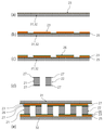
1 is a longitudinal sectional view schematically showing a conventional
The p-type
However, in the conventional
Further, in the
The present invention has been conceived to solve the problems of the conventional thermoelectric module as described above. Unlike the conventional technology, the thermoelectric module includes the upper substrate and the lower substrate, and the module is filled with the polymer material. Since there is no such a high ceramic substrate, a temperature difference between the thermoelectric elements can be largely maintained, and the thermoelectric performance can be remarkably improved. Unlike the existing technology, when a polymer material for filling is used as a stretchable polymer material, flexibility and stretchability And to provide a thermoelectric module manufactured by the method.
According to the present invention, there is provided a method of manufacturing a semiconductor device, comprising: (a) forming a substrate peeling layer on a temporary upper substrate and a temporary lower substrate; (b) forming electrodes on the substrate peeling layer; (c) arranging and bonding the p-type thermoelectric elements and the n-type thermoelectric elements to the electrodes; (d) filling the inside of the module, in which the p-type thermoelectric elements and the n-type thermoelectric elements are bonded to electrodes, with a polymer; (e) peeling off the temporary upper substrate and the temporary lower substrate from the module filled with the polymer; And (f) removing the substrate peeling layer from the module from which the temporary upper substrate and the temporary lower substrate are removed. The present invention also provides a method of manufacturing a thermoelectric module.
Preferably, the temporary top board and temporarily lower substrate is a silicon (Si), glass (SiO 2), alumina (Al 2 O 3), aluminum nitride (AlN), silicon carbide (SiC), silicon nitride (Si 3 N 4 , MgO, Ni, Cu, Sn, Ag, Al, Au, Pt, Fe, , At least one of chromium (Cr), titanium (Ti), tantalum (Ta), and tungsten (W).
Preferably, the substrate delamination layer is formed of a material selected from the group consisting of Ni, Cu, Sn, Ag, Al, Au, Pt, (Cr), titanium (Ti), tantalum (Ta), and tungsten (W).
Preferably, the substrate delamination layer is formed by any one of vacuum deposition, electron beam deposition, electroplating, electroless plating, sputtering, screen printing, chemical vapor deposition, MBE (Molecular Beam Epitaxy), and MOCVD (Metal Organic Chemical Vapor Deposition) And two or more methods are provided in combination.
Preferably, the electrode is made of at least one selected from the group consisting of copper (Cu), nickel (Ni), tin (Sn), silver (Ag), aluminum (Al), gold (Au), platinum ), Titanium (Ti), tantalum (Ta), tungsten (W), carbon nanotubes (CNT), and graphene.
Preferably, the electrode is formed of one or more of electroplating, electroless plating, vacuum deposition, sputtering, screen printing, electron beam deposition, chemical vapor deposition, MBE (Molecular Beam Epitaxy), and MOCVD (Metal Organic Chemical Vapor Deposition) Or a combination thereof.
Preferably, when the electrode is formed by a screen printing method, the electrode may be formed of at least one selected from the group consisting of copper (Cu), nickel (Ni), tin (Sn), silver (Ag), aluminum (Al) A paste containing any one or two or more of Pt, Fe, Cr, Ti, Ta, W, CNT and graphene is used .
Preferably, the electrode is made of at least one selected from the group consisting of copper (Cu), nickel (Ni), tin (Sn), silver (Ag), aluminum (Al), gold (Au), platinum ), Titanium (Ti), tantalum (Ta), and tungsten (W) are arranged and bonded to a substrate peeling layer.
Preferably, the p-type thermoelectric element is made of p-type (Bi, Sb) 2 Te 3 , Sb 2 Te 3 , Bi 2 Te 3 , SiGe, Pb, Sn Te, PbTe, skutterudite, AgPb m SbTe 2 + m , Zn 4 Sb 3 , MnSi, FeSi 2 , Mg 2 Si, Chromel alloy, platinum-rhodium alloy, iron, copper and Nichrosil alloy, , A nanocomposite, a thin film, a superlattice, a nanotube, a quantum dot, or a combination of two or more thereof.
Preferably, the n-type thermoelectric elements are n-type Bi 2 (Te, Se) 3 , Bi 2 Te 3, (Bi, Sb) 2 Te 3, SiGe, (Pb, Ge) Te, PbTe, skutterudite, AgPb m A single crystal made of any one or a combination of two or more of SbTe 2 + m , FeSi 2 , CoSi, Mg 2 Si, platinum-rhodium alloy, Alumel alloy, Constantant alloy, Nisil alloy, , A nanocomposite, a thin film, a superlattice, a nanotube, a quantum dot, or a combination of two or more thereof.
Preferably, the polymer comprises at least one of PDMS (polydimethylsiloxane), silicone, rubber, polyurethane, polyimide, epoxy, phenol, polyester, polycarbonate, polyarylate, polyether sulfone, And the like.
Preferably, the step (b) further comprises forming a device junction layer on the surfaces of the electrodes, wherein the device junction layer is formed by bonding the p-type thermoelectric elements and the n-type thermoelectric elements to the electrodes .
Preferably, the device junction layer is provided by one or more of solder, a conductive adhesive, a conductive adhesive film, an anisotropic conductive adhesive, and an anisotropic conductive adhesive film.
Preferably, when the solder is used as a device junction layer, the solder may be formed of at least one selected from the group consisting of silver (Ag), copper (Cu), bismuth (Bi), indium (In) Sb), lead (Pb), and gold (Au).
Preferably, the method further comprises the step of providing a barrier layer on the p-type thermoelectric elements and the n-type thermoelectric elements before the step (c).
Preferably, the barrier layer comprises at least one of nickel (Ni), copper (Cu), tin (Sn), silver (Ag), aluminum (Al), gold (Au), platinum (Pt) (Ti), tantalum (Ta), tungsten (W), or a combination of two or more metals.
Preferably, the barrier layer is formed of one or both of electroplating, electroless plating, vacuum deposition, sputtering, screen printing, electron beam deposition, chemical vapor deposition, MBE (Molecular Beam Epitaxy), and MOCVD (Metal Organic Chemical Vapor Deposition) The above-mentioned method is characterized by being combined.
Preferably, after the step (f), the module having the substrate peeling layer removed may be provided with an insulating layer.
Preferably, the insulating layer is formed of a material selected from the group consisting of parylene, epoxy, phenol, polyimide, polyester, polycarbonate, polyarylate, polyether sulfone, Teflon, FR4, silicone, polydimethylsiloxane Urethane, or by coating or laminating a polymer material containing at least one of the urethane and urethane.
According to another aspect of the present invention, there is provided a method of manufacturing a semiconductor device, comprising: (a) forming a substrate peeling layer on a temporary lower substrate; (b) forming electrodes on the substrate peeling layer of the temporary lower substrate; (c) forming p-type thermoelectric elements and n-type thermoelectric elements on the electrodes; (d) forming a substrate peeling layer on the temporary upper substrate; (e) forming electrodes on the substrate peeling layer of the temporary upper substrate; (f) arranging and bonding the electrodes of the temporary upper substrate to the p-type thermoelectric elements and the n-type thermoelectric elements of the temporary lower substrate; (g) filling the inside of the module in which the p-type thermoelectric elements and the n-type thermoelectric elements are bonded to the electrodes with a polymer; (h) peeling off the temporary upper substrate and the temporary lower substrate from the module filled with the polymer; And (i) removing both the substrate peeling layer from the module from which the temporary upper substrate and the temporary lower substrate are removed.
Preferably, the temporary top board and temporarily lower substrate is a silicon (Si), glass (SiO 2), alumina (Al 2 O 3), aluminum nitride (AlN), silicon carbide (SiC), silicon nitride (Si 3 N 4 , MgO, Ni, Cu, Sn, Ag, Al, Au, Pt, Fe, , At least one of chromium (Cr), titanium (Ti), tantalum (Ta), and tungsten (W).
Preferably, the substrate delamination layer is formed of a material selected from the group consisting of Ni, Cu, Sn, Ag, Al, Au, Pt, (Cr), titanium (Ti), tantalum (Ta), and tungsten (W).
Preferably, the substrate delamination layer is formed by any one of vacuum deposition, electron beam deposition, electroplating, electroless plating, sputtering, screen printing, chemical vapor deposition, MBE (Molecular Beam Epitaxy), and MOCVD (Metal Organic Chemical Vapor Deposition) And two or more methods are provided in combination.
Preferably, the electrode is made of at least one selected from the group consisting of copper (Cu), nickel (Ni), tin (Sn), silver (Ag), aluminum (Al), gold (Au), platinum ), Titanium (Ti), tantalum (Ta), tungsten (W), carbon nanotubes (CNT), and graphene.
Preferably, the electrode is formed of one or more of electroplating, electroless plating, vacuum deposition, sputtering, screen printing, electron beam deposition, chemical vapor deposition, MBE (Molecular Beam Epitaxy), and MOCVD (Metal Organic Chemical Vapor Deposition) Or a combination thereof.
Preferably, when the electrode is formed by a screen printing method, the electrode may be formed of at least one selected from the group consisting of copper (Cu), nickel (Ni), tin (Sn), silver (Ag), aluminum (Al) A paste containing any one or two or more of Pt, Fe, Cr, Ti, Ta, W, CNT and graphene is used .
Preferably, the electrode is made of at least one selected from the group consisting of copper (Cu), nickel (Ni), tin (Sn), silver (Ag), aluminum (Al), gold (Au), platinum ), Titanium (Ti), tantalum (Ta), and tungsten (W) are arranged and bonded to a substrate peeling layer.
Preferably, the p-type thermoelectric element is made of p-type (Bi, Sb) 2 Te 3 , Sb 2 Te 3 , Bi 2 Te 3 , SiGe, Pb, Sn Te, PbTe, skutterudite, AgPb m SbTe 2 + m , Zn 4 Sb 3 , MnSi, FeSi 2 , Mg 2 Si, Chromel alloy, platinum-rhodium alloy, iron, copper and Nichrosil alloy, , A nanocomposite, a thin film, a superlattice, a nanotube, a quantum dot, or a combination of two or more thereof.
Preferably, the n-type thermoelectric elements are n-type Bi 2 (Te, Se) 3 , Bi 2 Te 3, (Bi, Sb) 2 Te 3, SiGe, (Pb, Ge) Te, PbTe, skutterudite, AgPb m A single crystal made of any one or a combination of two or more of SbTe 2 + m , FeSi 2 , CoSi, Mg 2 Si, platinum-rhodium alloy, Alumel alloy, Constantant alloy, Nisil alloy, , A nanocomposite, a thin film, a superlattice, a nanotube, a quantum dot, or a combination of two or more thereof.
Preferably, the polymer comprises at least one of PDMS (polydimethylsiloxane), silicone, rubber, polyurethane, polyimide, epoxy, phenol, polyester, polycarbonate, polyarylate, polyether sulfone, And the like.
Preferably, after step (e), forming a device junction layer on the surface of the electrodes formed on the substrate peeling layer of the temporary upper substrate; And bonding the p-type thermoelectric elements and the n-type thermoelectric elements to the electrodes using the device junction layer.
Preferably, the device junction layer is provided by one or more of solder, a conductive adhesive, a conductive adhesive film, an anisotropic conductive adhesive, and an anisotropic conductive adhesive film.
Preferably, when the solder is used as a device junction layer, the solder may be formed of at least one selected from the group consisting of silver (Ag), copper (Cu), bismuth (Bi), indium (In) Sb), lead (Pb), and gold (Au).
Preferably, after step (c), providing a barrier layer to the p-type thermoelectric elements and the n-type thermoelectric elements; And further comprising:
Preferably, the barrier layer comprises at least one of nickel (Ni), copper (Cu), tin (Sn), silver (Ag), aluminum (Al), gold (Au), platinum (Pt) (Ti), tantalum (Ta), tungsten (W), or a combination of two or more metals.
Preferably, the barrier layer is formed of one or both of electroplating, electroless plating, vacuum deposition, sputtering, screen printing, electron beam deposition, chemical vapor deposition, MBE (Molecular Beam Epitaxy), and MOCVD (Metal Organic Chemical Vapor Deposition) The above-mentioned method is characterized by being combined.
Preferably, after the step (i), the module having the substrate delamination layer removed may be provided with an insulating layer.
Preferably, the insulating layer is formed of a material selected from the group consisting of parylene, epoxy, phenol, polyimide, polyester, polycarbonate, polyarylate, polyether sulfone, Teflon, FR4, silicone, polydimethylsiloxane Urethane, or by coating or laminating a polymer material containing at least one of the urethane and urethane.
According to another aspect of the present invention, there is provided a method of manufacturing a semiconductor device, comprising: (a) forming a substrate peeling layer on a temporary lower substrate; (b) forming electrodes on the substrate peeling layer of the temporary lower substrate; (c) forming p-type thermoelectric elements and n-type thermoelectric elements on the electrodes; (d) forming an upper electrode electrically connecting the p-type thermoelectric elements and the n-type thermoelectric elements; (e) filling the inside of the module in which the p-type thermoelectric elements and the n-type thermoelectric elements are formed with electrodes with a polymer; (f) peeling off the temporary lower substrate from the module filled with the polymer; And (g) removing the substrate delamination layer from the module from which the temporary lower substrate has been removed. The present invention also provides a method of manufacturing a thermoelectric module.
Preferably, the temporary lower substrate is a silicon (Si), glass (SiO 2), alumina (Al 2 O 3), aluminum nitride (AlN), silicon carbide (SiC), silicon nitride (Si 3 N 4,) (Mg), Ni, Cu, Sn, Ag, Al, Au, Pt, Fe, Cr ), Titanium (Ti), tantalum (Ta), and tungsten (W).
Preferably, the substrate delamination layer is formed of a material selected from the group consisting of Ni, Cu, Sn, Ag, Al, Au, Pt, (Cr), titanium (Ti), tantalum (Ta), and tungsten (W).
Preferably, the substrate delamination layer is formed by any one of vacuum deposition, electron beam deposition, electroplating, electroless plating, sputtering, screen printing, chemical vapor deposition, MBE (Molecular Beam Epitaxy), and MOCVD (Metal Organic Chemical Vapor Deposition) And two or more methods are provided in combination.
Preferably, the electrode is made of at least one selected from the group consisting of copper (Cu), nickel (Ni), tin (Sn), silver (Ag), aluminum (Al), gold (Au), platinum ), Titanium (Ti), tantalum (Ta), tungsten (W), carbon nanotubes (CNT), and graphene.
Preferably, the electrode is formed of one or more of electroplating, electroless plating, vacuum deposition, sputtering, screen printing, electron beam deposition, chemical vapor deposition, MBE (Molecular Beam Epitaxy), and MOCVD (Metal Organic Chemical Vapor Deposition) Or a combination thereof.
Preferably, when the electrode is formed by a screen printing method, the electrode may be formed of at least one selected from the group consisting of copper (Cu), nickel (Ni), tin (Sn), silver (Ag), aluminum (Al) A paste containing any one or two or more of Pt, Fe, Cr, Ti, Ta, W, CNT and graphene is used .
Preferably, the electrode is made of at least one selected from the group consisting of copper (Cu), nickel (Ni), tin (Sn), silver (Ag), aluminum (Al), gold (Au), platinum ), Titanium (Ti), tantalum (Ta), and tungsten (W) are arranged and bonded to a substrate peeling layer.
Preferably, the p-type thermoelectric element is made of p-type (Bi, Sb) 2 Te 3 , Sb 2 Te 3 , Bi 2 Te 3 , SiGe, Pb, Sn Te, PbTe, skutterudite, AgPb m SbTe 2 + m , Zn 4 Sb 3 , MnSi, FeSi 2 , Mg 2 Si, Chromel alloy, platinum-rhodium alloy, iron, copper and Nichrosil alloy, , A nanocomposite, a thin film, a superlattice, a nanotube, a quantum dot, or a combination of two or more thereof.
Preferably, the n-type thermoelectric elements are n-type Bi 2 (Te, Se) 3 , Bi 2 Te 3, (Bi, Sb) 2 Te 3, SiGe, (Pb, Ge) Te, PbTe, skutterudite, AgPb m A single crystal made of any one or a combination of two or more of SbTe 2 + m , FeSi 2 , CoSi, Mg 2 Si, platinum-rhodium alloy, Alumel alloy, Constantant alloy, Nisil alloy, , A nanocomposite, a thin film, a superlattice, a nanotube, a quantum dot, or a combination of two or more thereof.
Preferably, the polymer comprises at least one of PDMS (polydimethylsiloxane), silicone, rubber, polyurethane, polyimide, epoxy, phenol, polyester, polycarbonate, polyarylate, polyether sulfone, And the like.
Preferably, after the step (g), the module having the substrate delamination layer removed is provided with an insulating layer.
Preferably, the insulating layer is formed of a material selected from the group consisting of parylene, epoxy, phenol, polyimide, polyester, polycarbonate, polyarylate, polyether sulfone, Teflon, FR4, silicone, polydimethylsiloxane Urethane, or by coating or laminating a polymer material containing at least one of the urethane and urethane.
According to another aspect of the present invention, there is provided a thermoelectric module manufactured by the method for manufacturing a thermoelectric module according to any one of the above-described features.
According to the present invention, since a thermoelectric module having no upper and lower substrates and filling a module with a polymer material is provided, a temperature difference between the thermoelectric elements can be largely maintained because there is no ceramic substrate having a high thermal resistance unlike the existing technology It is possible to remarkably improve the thermoelectric performance.
In addition, when the polymer material for internal filling is used as a stretchable polymer material, flexibility and stretchability can be imparted to the thermoelectric module unlike the existing technology.
1 is a schematic cross-sectional view of a thermoelectric module according to the prior art;
2 is a schematic cross-sectional view of a stretchable thermoelectric module in which an upper substrate and a lower substrate are absent and the inside is filled with a stretchable polymer according to the present invention.
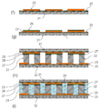
3 and 4 are cross-sectional views illustrating a method of manufacturing a thermoelectric module according to a first embodiment and a second embodiment of the present invention. More specifically, FIG. 3 (a) 3 (b) is a cross-sectional view of the
5A to 5C are cross-sectional views illustrating a method of manufacturing a thermoelectric module according to a third embodiment of the present invention. More specifically, FIG. 5A is a cross- 5 (b) is a sectional view of the temporary
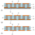
8A and 9B are cross-sectional views illustrating a method of manufacturing a thermoelectric module according to a fourth embodiment of the present invention. Specifically, FIG. 8A is a cross- 8 (b) is a cross-sectional view of the temporary
10 is a cross-sectional view of a stretchable
11 is a cross-sectional view of a stretchable
≪ Example 1 >
3 (a), a nickel (Ni)
The solder paste is applied by screen printing to the surfaces of the
The p-type (Bi 0.25 Sb 0.75 ) 2 Te 3 pressure sintered body was cut into a size of 2 mm x 2 mm and a height of 3 mm and electroless plating of nickel was carried out on the upper surface and the lower surface to a thickness of 2 탆, Type
The p-type
The inside of the thermoelectric module to which the temporary
4 (g), a thermoelectric module filled with the PDMS
As shown in FIG. 4 (h), the thermoelectric module, in which the temporary
In this embodiment, unlike the conventional technology, there is no rigid and
The maximum power generation output P o of the
![]()
The number in the formula 1 m is a p-type thermoelectric elements (13,21) and an n-type thermoelectric elements (14,22) pair (pn thermoelectric element pair) constituting the thermoelectric modules (10,20), α is the p-type R is the internal resistance of the
≪ Example 2 >
A nickel
The solder paste is applied to the surface of the
The p-type (Bi 0.25 Sb 0.75 ) 2 Te 3 pressure sintered body was cut into a size of 2 mm x 2 mm and a height of 3 mm and electroless plating of nickel on the upper and lower surfaces was performed to form a barrier layer 27 ), a p-type
The p-type
As described above, the module formed by using the temporary
The module in which the temporary
≪ Example 3 >
As shown in Fig. 5 (a), a nickel
A photoresist pattern for forming the p-type
Thereafter, a photoresist pattern for forming the n-type
After the p-type
Then, a nickel
A photoresist pattern is formed on the temporary
The
6 (i), the inside of the thermoelectric module to which the temporary
6 (k), the thermoelectric module from which the temporary
<Example 4>
A nickel
A photoresist pattern for forming the p-type
A photoresist pattern is formed on the temporary
9 (f), the inside of the thermoelectric module provided on the temporary
Then, as shown in FIG. 9 (h), the thermoelectric module from which the temporary
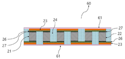
10, after removing the nickel
Preferably, the insulating
In this embodiment, the
In this embodiment, a
In this embodiment, a
In this embodiment, the
In the present embodiment, the flexible
In the
The solder used as the
In this embodiment, PDMS (polydimethylsiloxane) is used as the
In this embodiment, a stretchable
In this embodiment, (Bi 0.25 Sb 0.75 ) 2 Te 3 pressure sintered body was used as the p-type
In this embodiment, Bi 2 (Te 0.95 Se 0.05 ) 3 pressure sintered body was used as the n-type
In this embodiment, the
In this embodiment, the
In this embodiment, the
In the present invention, the
As described above, an optimal embodiment has been disclosed in the drawings and specification. Although specific terms have been employed herein, they are used for purposes of illustration only and are not intended to limit the scope of the invention as defined in the claims or the claims. Therefore, those skilled in the art will appreciate that various modifications and equivalent embodiments are possible without departing from the scope of the present invention. Accordingly, the true scope of the present invention should be determined by the technical idea of the appended claims.
10: Thermoelectric module by existing technology
11.
13. p-type thermoelectric element 14. n-type thermoelectric element
15.
17. Barrier layer
20. The thermoelectric module
21. p-type
23.
25.
27. Barrier layer
31. Temporary
60. A thermoelectric module having an insulating layer according to the present invention
61. Insulation layer
70. A thermoelectric module according to the present invention,
Claims (52)
(b) forming electrodes on the substrate peeling layer;
(c) arranging and bonding the p-type thermoelectric elements and the n-type thermoelectric elements to the electrodes;
(d) filling the inside of the module, in which the p-type thermoelectric elements and the n-type thermoelectric elements are bonded to electrodes, with a polymer;
(e) peeling off the temporary upper substrate and the temporary lower substrate from the module filled with the polymer; And
(f) removing the substrate peeling layer from the module from which the temporary upper substrate and the temporary lower substrate are removed; Wherein the thermoelectric module is a thermoelectric module.
The temporary upper substrate and a temporary lower substrate is a silicon (Si), glass (SiO 2), alumina (Al 2 O 3), aluminum nitride (AlN), silicon carbide (SiC), silicon nitride (Si 3 N 4,) (Mg), Ni, Cu, Sn, Ag, Al, Au, Pt, Fe, Cr ), Titanium (Ti), tantalum (Ta), and tungsten (W).
The substrate delamination layer may include at least one of Ni, Cu, Sn, Ag, Au, Pt, Fe, Cr, Wherein the thermoelectric module comprises a combination of a metal having a composition containing at least one of titanium (Ti), tantalum (Ta), and tungsten (W).
The substrate delamination layer may be formed by any one or more of the methods of vacuum deposition, electron beam deposition, electroplating, electroless plating, sputtering, screen printing, chemical vapor deposition, MBE (Molecular Beam Epitaxy), and MOCVD (Metal Organic Chemical Vapor Deposition) Wherein the thermoelectric module is provided in combination with the thermoelectric module.
The electrode may be formed of at least one selected from the group consisting of copper (Cu), nickel (Ni), tin (Sn), silver (Ag), aluminum (Al), gold (Au), platinum (Pt), iron (Fe) Ti, tantalum (W), carbon nanotubes (CNT) and graphene, or a combination of two or more thereof.
The electrode may be formed by combining any one or more of electroplating, electroless plating, vacuum deposition, sputtering, screen printing, electron beam deposition, chemical vapor deposition, MBE (Molecular Beam Epitaxy), and MOCVD (Metal Organic Chemical Vapor Deposition) Wherein the thermoelectric module comprises a thermoelectric module.
When the electrode is formed by a screen printing method, the electrode may be formed of a metal such as copper (Cu), nickel (Ni), tin (Sn), silver (Ag), aluminum (Al), gold (Au), platinum A paste containing any one or more of Fe, Cr, Ti, Ta, W, CNT, and graphene is used. Of the thermoelectric module.
The electrode may be formed of at least one selected from the group consisting of copper (Cu), nickel (Ni), tin (Sn), silver (Ag), aluminum (Al), gold (Au), platinum (Pt), iron (Fe) Wherein a metal piece having a composition containing at least one of Ti, Ti, Ta and W is arranged and bonded to the substrate peeling layer.
The p-type thermoelectric element is a p-type (Bi, Sb) 2 Te 3 , Sb 2 Te 3, Bi 2 Te 3, SiGe, (Pb, Sn) Te, PbTe, skutterudite, AgPb m SbTe 2 + m, Zn 4 Sb 3, MnSi, FeSi 2, Mg 2 Si, chroman Mel (Chromel) alloy, a platinum-rhodium alloy, iron, copper, nikeuro chamber (Nichrosil) consisting of any one or a combination of two or more of the alloy single crystal, a pressure-sintered body, nanocomposite, A superlattice, a nanotube, a quantum dot, or a combination of two or more thereof.
The n-type thermoelectric element is made of n-type Bi 2 (Te, Se) 3 , Bi 2 Te 3 , (Bi, Sb) 2 Te 3 , SiGe, (Pb, Ge) Te, PbTe, skutterudite, AgPb m SbTe 2 + m A pressure-sintered body, a nanocomposite, a sintered body made of any one or a combination of two or more of FeSi 2 , CoSi, Mg 2 Si, platinum-rhodium alloy, Alumel alloy, Constantant alloy, A superlattice, a nanotube, a quantum dot, or a combination of two or more thereof.
The polymer may be a polymer containing at least one of PDMS (polydimethylsiloxane), silicone, rubber, polyurethane, polyimide, epoxy, phenol, polyester, polycarbonate, polyarylate, polyether sulfone, Wherein the thermoelectric module is a thermoelectric module.
After the step (b)
And forming a device junction layer on the surface of the electrodes, wherein the device junction layer is used to bond the p-type thermoelectric elements and the n-type thermoelectric elements to the electrodes.
Wherein the device junction layer is provided by one or more of solder, a conductive adhesive, a conductive adhesive film, an anisotropic conductive adhesive, and an anisotropic conductive adhesive film.
When the solder is used as a device junction layer, the solder may contain at least one selected from the group consisting of silver (Ag), copper (Cu), bismuth (Bi), indium (In), zinc (Zn), antimony (Pb), and gold (Au). The method of manufacturing a thermoelectric module according to claim 1,
Prior to step (c)
and providing a barrier layer on the p-type thermoelectric elements and the n-type thermoelectric elements.
The barrier layer may include at least one of nickel, copper, tin, silver, aluminum, gold, platinum, iron, chromium, titanium, Wherein the thermoelectric module is provided with a single layer or a multilayer of a combination of a metal having a composition containing any one or more of Ti, Ta, and W.
The barrier layer may be formed by a combination of any one or more of electroplating, electroless plating, vacuum deposition, sputtering, screen printing, electron beam deposition, chemical vapor deposition, MBE (Molecular Beam Epitaxy), and MOCVD (Metal Organic Chemical Vapor Deposition) Wherein the thermoelectric module comprises a thermoelectric module.
After the step (f)
And forming an insulation layer on the module from which the substrate release layer has been removed.
The insulating layer may include at least one of parylene, epoxy, phenol, polyimide, polyester, polycarbonate, polyarylate, polyether sulfone, Teflon, FR4, silicone, polydimethylsiloxane Wherein the thermoelectric module is formed using a coating or lamination of a polymer material including a thermosetting resin.
(b) forming electrodes on the substrate peeling layer of the temporary lower substrate;
(c) forming p-type thermoelectric elements and n-type thermoelectric elements on the electrodes;
(d) forming a substrate peeling layer on the temporary upper substrate;
(e) forming electrodes on the substrate peeling layer of the temporary upper substrate;
(f) arranging and bonding the electrodes of the temporary upper substrate to the p-type thermoelectric elements and the n-type thermoelectric elements of the temporary lower substrate;
(g) filling the inside of the module in which the p-type thermoelectric elements and the n-type thermoelectric elements are bonded to the electrodes with a polymer;
(h) peeling off the temporary upper substrate and the temporary lower substrate from the module filled with the polymer; And
(i) removing both the substrate peeling layer from the module from which the temporary upper substrate and the temporary lower substrate are removed.
The temporary upper substrate and a temporary lower substrate is a silicon (Si), glass (SiO 2), alumina (Al 2 O 3), aluminum nitride (AlN), silicon carbide (SiC), silicon nitride (Si 3 N 4,) (Mg), Ni, Cu, Sn, Ag, Al, Au, Pt, Fe, Cr ), Titanium (Ti), tantalum (Ta), and tungsten (W).
The substrate delamination layer may include at least one of Ni, Cu, Sn, Ag, Au, Pt, Fe, Cr, Wherein the thermoelectric module comprises a combination of a metal having a composition containing at least one of titanium (Ti), tantalum (Ta), and tungsten (W).
The substrate delamination layer may be formed by any one or more of the methods of vacuum deposition, electron beam deposition, electroplating, electroless plating, sputtering, screen printing, chemical vapor deposition, MBE (Molecular Beam Epitaxy), and MOCVD (Metal Organic Chemical Vapor Deposition) Wherein the thermoelectric module is provided in combination with the thermoelectric module.
The electrode may be formed of at least one selected from the group consisting of copper (Cu), nickel (Ni), tin (Sn), silver (Ag), aluminum (Al), gold (Au), platinum (Pt), iron (Fe) Ti, tantalum (W), carbon nanotubes (CNT) and graphene, or a combination of two or more thereof.
The electrode may be formed by combining any one or more of electroplating, electroless plating, vacuum deposition, sputtering, screen printing, electron beam deposition, chemical vapor deposition, MBE (Molecular Beam Epitaxy), and MOCVD (Metal Organic Chemical Vapor Deposition) Wherein the thermoelectric module comprises a thermoelectric module.
When the electrode is formed by a screen printing method, the electrode may be formed of a metal such as copper (Cu), nickel (Ni), tin (Sn), silver (Ag), aluminum (Al), gold (Au), platinum A paste containing any one or more of Fe, Cr, Ti, Ta, W, CNT, and graphene is used. Of the thermoelectric module.
The electrode may be formed of at least one selected from the group consisting of copper (Cu), nickel (Ni), tin (Sn), silver (Ag), aluminum (Al), gold (Au), platinum (Pt), iron (Fe) Wherein a metal piece having a composition containing at least one of Ti, Ti, Ta and W is arranged and bonded to the substrate peeling layer.
The p-type thermoelectric element is a p-type (Bi, Sb) 2 Te 3 , Sb 2 Te 3, Bi 2 Te 3, SiGe, (Pb, Sn) Te, PbTe, skutterudite, AgPb m SbTe 2 + m, Zn 4 Sb 3, MnSi, FeSi 2, Mg 2 Si, chroman Mel (Chromel) alloy, a platinum-rhodium alloy, iron, copper, nikeuro chamber (Nichrosil) consisting of any one or a combination of two or more of the alloy single crystal, a pressure-sintered body, nanocomposite, A superlattice, a nanotube, a quantum dot, or a combination of two or more thereof.
The n-type thermoelectric element is made of n-type Bi 2 (Te, Se) 3 , Bi 2 Te 3 , (Bi, Sb) 2 Te 3 , SiGe, (Pb, Ge) Te, PbTe, skutterudite, AgPb m SbTe 2 + m A pressure-sintered body, a nanocomposite, a sintered body made of any one or a combination of two or more of FeSi 2 , CoSi, Mg 2 Si, platinum-rhodium alloy, Alumel alloy, Constantant alloy, A superlattice, a nanotube, a quantum dot, or a combination of two or more thereof.
The polymer may be a polymer containing at least one of PDMS (polydimethylsiloxane), silicone, rubber, polyurethane, polyimide, epoxy, phenol, polyester, polycarbonate, polyarylate, polyether sulfone, Wherein the thermoelectric module is a thermoelectric module.
After the step (e)
Forming a device junction layer on surfaces of the electrodes formed on the substrate peeling layer of the temporary upper substrate; Wherein the p-type thermoelectric elements and the n-type thermoelectric elements are bonded to the electrodes using the device junction layer.
Wherein the device junction layer is provided by one or more of solder, a conductive adhesive, a conductive adhesive film, an anisotropic conductive adhesive, and an anisotropic conductive adhesive film.
When the solder is used as a device junction layer, the solder may contain at least one selected from the group consisting of silver (Ag), copper (Cu), bismuth (Bi), indium (In), zinc (Zn), antimony (Pb), and gold (Au). The method of manufacturing a thermoelectric module according to claim 1,
After the step (c)
providing a barrier layer on the p-type thermoelectric elements and the n-type thermoelectric elements; Further comprising the steps of:
The barrier layer may include at least one of nickel, copper, tin, silver, aluminum, gold, platinum, iron, chromium, titanium, Wherein the thermoelectric module is provided with a single layer or a multilayer of a combination of a metal having a composition containing any one or more of Ti, Ta, and W.
The barrier layer may be formed by a combination of any one or more of electroplating, electroless plating, vacuum deposition, sputtering, screen printing, electron beam deposition, chemical vapor deposition, MBE (Molecular Beam Epitaxy), and MOCVD (Metal Organic Chemical Vapor Deposition) Wherein the thermoelectric module comprises a thermoelectric module.
After the step (i)
And forming an insulation layer on the module from which the substrate release layer has been removed.
The insulating layer may include at least one of parylene, epoxy, phenol, polyimide, polyester, polycarbonate, polyarylate, polyether sulfone, Teflon, FR4, silicone, polydimethylsiloxane Wherein the thermoelectric module is formed using a coating or lamination of a polymer material including a thermosetting resin.
(b) forming electrodes on the substrate peeling layer of the temporary lower substrate;
(c) forming p-type thermoelectric elements and n-type thermoelectric elements on the electrodes;
(d) forming an upper electrode electrically connecting the p-type thermoelectric elements and the n-type thermoelectric elements;
(e) filling the inside of the module in which the p-type thermoelectric elements and the n-type thermoelectric elements are formed with electrodes with a polymer;
(f) peeling off the temporary lower substrate from the module filled with the polymer; And
(g) removing the substrate peeling layer from the module from which the temporary lower substrate has been removed; Wherein the thermoelectric module is a thermoelectric module.
The temporary lower substrate is a silicon (Si), glass (SiO 2), alumina (Al 2 O 3), aluminum nitride (AlN), silicon carbide (SiC), silicon nitride (Si 3 N 4,), magnesium oxide ( (Mg), Ni, Cu, Sn, Ag, Al, Au, Pt, Fe, Cr, Ti), tantalum (Ta), and tungsten (W).
The substrate delamination layer may include at least one of Ni, Cu, Sn, Ag, Au, Pt, Fe, Cr, Wherein the thermoelectric module comprises a combination of a metal having a composition containing at least one of titanium (Ti), tantalum (Ta), and tungsten (W).
The substrate delamination layer may be formed by any one or more of the methods of vacuum deposition, electron beam deposition, electroplating, electroless plating, sputtering, screen printing, chemical vapor deposition, MBE (Molecular Beam Epitaxy), and MOCVD (Metal Organic Chemical Vapor Deposition) Wherein the thermoelectric module is provided in combination with the thermoelectric module.
The electrode may be formed of at least one selected from the group consisting of copper (Cu), nickel (Ni), tin (Sn), silver (Ag), aluminum (Al), gold (Au), platinum (Pt), iron (Fe) Ti, tantalum (W), carbon nanotubes (CNT) and graphene, or a combination of two or more thereof.
The electrode may be formed by combining any one or more of electroplating, electroless plating, vacuum deposition, sputtering, screen printing, electron beam deposition, chemical vapor deposition, MBE (Molecular Beam Epitaxy), and MOCVD (Metal Organic Chemical Vapor Deposition) Wherein the thermoelectric module comprises a thermoelectric module.
When the electrode is formed by a screen printing method, the electrode may be formed of a metal such as copper (Cu), nickel (Ni), tin (Sn), silver (Ag), aluminum (Al), gold (Au), platinum A paste containing any one or more of Fe, Cr, Ti, Ta, W, CNT, and graphene is used. Of the thermoelectric module.
The electrode may be formed of at least one selected from the group consisting of copper (Cu), nickel (Ni), tin (Sn), silver (Ag), aluminum (Al), gold (Au), platinum (Pt), iron (Fe) Wherein a metal piece having a composition containing at least one of Ti, Ti, Ta and W is arranged and bonded to the substrate peeling layer.
The p-type thermoelectric element is a p-type (Bi, Sb) 2 Te 3 , Sb 2 Te 3, Bi 2 Te 3, SiGe, (Pb, Sn) Te, PbTe, skutterudite, AgPb m SbTe 2 + m, Zn 4 Sb 3, MnSi, FeSi 2, Mg 2 Si, chroman Mel (Chromel) alloy, a platinum-rhodium alloy, iron, copper, nikeuro chamber (Nichrosil) consisting of any one or a combination of two or more of the alloy single crystal, a pressure-sintered body, nanocomposite, A superlattice, a nanotube, a quantum dot, or a combination of two or more thereof.
The n-type thermoelectric element is made of n-type Bi 2 (Te, Se) 3 , Bi 2 Te 3 , (Bi, Sb) 2 Te 3 , SiGe, (Pb, Ge) Te, PbTe, skutterudite, AgPb m SbTe 2 + m A pressure-sintered body, a nanocomposite, a sintered body made of any one or a combination of two or more of FeSi 2 , CoSi, Mg 2 Si, platinum-rhodium alloy, Alumel alloy, Constantant alloy, A superlattice, a nanotube, a quantum dot, or a combination of two or more thereof.
The polymer may be a polymer containing at least one of PDMS (polydimethylsiloxane), silicone, rubber, polyurethane, polyimide, epoxy, phenol, polyester, polycarbonate, polyarylate, polyether sulfone, Wherein the thermoelectric module is a thermoelectric module.
After the step (g)
And forming an insulation layer on the module from which the substrate release layer has been removed.
The insulating layer may include at least one of parylene, epoxy, phenol, polyimide, polyester, polycarbonate, polyarylate, polyether sulfone, Teflon, FR4, silicone, polydimethylsiloxane Wherein the thermoelectric module is formed using a coating or lamination of a polymer material including a thermosetting resin.
Priority Applications (1)
| Application Number | Priority Date | Filing Date | Title |
|---|---|---|---|
| KR1020150113055A KR20170019109A (en) | 2015-08-11 | 2015-08-11 | Fabrication methods of stretchable thermoelectric modules and thermoelectric modules produced using the same methods |
Applications Claiming Priority (1)
| Application Number | Priority Date | Filing Date | Title |
|---|---|---|---|
| KR1020150113055A KR20170019109A (en) | 2015-08-11 | 2015-08-11 | Fabrication methods of stretchable thermoelectric modules and thermoelectric modules produced using the same methods |
Publications (1)
| Publication Number | Publication Date |
|---|---|
| KR20170019109A true KR20170019109A (en) | 2017-02-21 |
Family
ID=58313732
Family Applications (1)
| Application Number | Title | Priority Date | Filing Date |
|---|---|---|---|
| KR1020150113055A KR20170019109A (en) | 2015-08-11 | 2015-08-11 | Fabrication methods of stretchable thermoelectric modules and thermoelectric modules produced using the same methods |
Country Status (1)
| Country | Link |
|---|---|
| KR (1) | KR20170019109A (en) |
Cited By (2)
| Publication number | Priority date | Publication date | Assignee | Title |
|---|---|---|---|---|
| CN111244258A (en) * | 2020-01-20 | 2020-06-05 | 昆明理工大学 | Cu1.8S-based polycrystalline-amorphous metal composite thermoelectric material and preparation method thereof |
| CN113517384A (en) * | 2021-07-08 | 2021-10-19 | 西安电子科技大学 | Stretchable flexible thermoelectric device and manufacturing method thereof |
-
2015
- 2015-08-11 KR KR1020150113055A patent/KR20170019109A/en not_active Application Discontinuation
Cited By (4)
| Publication number | Priority date | Publication date | Assignee | Title |
|---|---|---|---|---|
| CN111244258A (en) * | 2020-01-20 | 2020-06-05 | 昆明理工大学 | Cu1.8S-based polycrystalline-amorphous metal composite thermoelectric material and preparation method thereof |
| CN111244258B (en) * | 2020-01-20 | 2022-01-18 | 昆明理工大学 | Cu1.8S-based polycrystalline-amorphous metal composite thermoelectric material and preparation method thereof |
| CN113517384A (en) * | 2021-07-08 | 2021-10-19 | 西安电子科技大学 | Stretchable flexible thermoelectric device and manufacturing method thereof |
| CN113517384B (en) * | 2021-07-08 | 2022-11-08 | 西安电子科技大学 | Stretchable flexible thermoelectric device and manufacturing method thereof |
Similar Documents
| Publication | Publication Date | Title |
|---|---|---|
| KR101493797B1 (en) | Flexible thermoelectric device using mesh substrate and fabricating method thereof | |
| US7679203B2 (en) | Methods of forming thermoelectric devices using islands of thermoelectric material and related structures | |
| KR101580041B1 (en) | Stretchable Thermoelectric Module | |
| JP5308577B2 (en) | Thermoelectric conversion element and manufacturing method thereof | |
| US10062827B2 (en) | Thermoelectric module | |
| US11024788B2 (en) | Flexible thermoelectric generator and method for fabricating the same | |
| JP5708174B2 (en) | Thermoelectric conversion device and manufacturing method thereof | |
| US20220181533A1 (en) | Thermoelectric conversion module | |
| KR101680422B1 (en) | Thermoelectric modules consisting of thermal-via electrodes and Fabrication method thereof | |
| US20180090660A1 (en) | Flexible thin-film based thermoelectric device with sputter deposited layer of n-type and p-type thermoelectric legs | |
| JP5653455B2 (en) | Thermoelectric conversion member | |
| JP2022518958A (en) | Thermoelectric element | |
| KR20170019109A (en) | Fabrication methods of stretchable thermoelectric modules and thermoelectric modules produced using the same methods | |
| KR101460880B1 (en) | Fabrication methods of thermoelectric thin film modules using moulds consisting of via-holes and thermoelectric thin film modules produced using the same method | |
| KR101460432B1 (en) | Fabrication methods of thermoelectric thin film modules using combined processes of adhesive flip chip bonding and solder reflow flip chip bonding and thermoelectric thin film modules produced using the same method | |
| WO2017164217A1 (en) | Thermoelectric conversion module | |
| KR20160002608A (en) | Thermoelectric modules consisting of thermal-via electrodes and Fabrication method thereof | |
| JP2004221109A (en) | Thermoelectric element module and manufacturing method therefor | |
| CN108713259B (en) | Thermoelectric conversion module | |
| KR20200010784A (en) | Flexible thermoelectric module and fabrication method thereof | |
| KR20150084314A (en) | Thermoelectric modules consisting of thermal-via electrodes and Fabrication method thereof | |
| KR20140110811A (en) | Fabrication methods of thermoelectric thin film modules using adhesive flip chip bonding and thermoelectric thin film modules produced using the same method | |
| KR20150084315A (en) | Thermoelectric modules consisting of thermal-via electrodes and Fabrication method thereof | |
| KR102456680B1 (en) | Thermoelectric element | |
| KR101474635B1 (en) | Fabrication methods of thermoelectric thin film modules using adhesive flip chip bonding and thermoelectric thin film modules produced using the same method |
Legal Events
| Date | Code | Title | Description |
|---|---|---|---|
| A201 | Request for examination | ||
| E902 | Notification of reason for refusal | ||
| E601 | Decision to refuse application |