EP1610369A1 - Plasma film-forming method and plasma film-forming apparatus - Google Patents
Plasma film-forming method and plasma film-forming apparatus Download PDFInfo
- Publication number
- EP1610369A1 EP1610369A1 EP04722947A EP04722947A EP1610369A1 EP 1610369 A1 EP1610369 A1 EP 1610369A1 EP 04722947 A EP04722947 A EP 04722947A EP 04722947 A EP04722947 A EP 04722947A EP 1610369 A1 EP1610369 A1 EP 1610369A1
- Authority
- EP
- European Patent Office
- Prior art keywords
- plasma
- microwave
- flat antenna
- antenna member
- assisted deposition
- Prior art date
- Legal status (The legal status is an assumption and is not a legal conclusion. Google has not performed a legal analysis and makes no representation as to the accuracy of the status listed.)
- Withdrawn
Links
Images




Classifications
-
- H—ELECTRICITY
- H01—ELECTRIC ELEMENTS
- H01J—ELECTRIC DISCHARGE TUBES OR DISCHARGE LAMPS
- H01J37/00—Discharge tubes with provision for introducing objects or material to be exposed to the discharge, e.g. for the purpose of examination or processing thereof
- H01J37/32—Gas-filled discharge tubes
- H01J37/32009—Arrangements for generation of plasma specially adapted for examination or treatment of objects, e.g. plasma sources
- H01J37/32192—Microwave generated discharge
-
- C—CHEMISTRY; METALLURGY
- C23—COATING METALLIC MATERIAL; COATING MATERIAL WITH METALLIC MATERIAL; CHEMICAL SURFACE TREATMENT; DIFFUSION TREATMENT OF METALLIC MATERIAL; COATING BY VACUUM EVAPORATION, BY SPUTTERING, BY ION IMPLANTATION OR BY CHEMICAL VAPOUR DEPOSITION, IN GENERAL; INHIBITING CORROSION OF METALLIC MATERIAL OR INCRUSTATION IN GENERAL
- C23C—COATING METALLIC MATERIAL; COATING MATERIAL WITH METALLIC MATERIAL; SURFACE TREATMENT OF METALLIC MATERIAL BY DIFFUSION INTO THE SURFACE, BY CHEMICAL CONVERSION OR SUBSTITUTION; COATING BY VACUUM EVAPORATION, BY SPUTTERING, BY ION IMPLANTATION OR BY CHEMICAL VAPOUR DEPOSITION, IN GENERAL
- C23C16/00—Chemical coating by decomposition of gaseous compounds, without leaving reaction products of surface material in the coating, i.e. chemical vapour deposition [CVD] processes
- C23C16/44—Chemical coating by decomposition of gaseous compounds, without leaving reaction products of surface material in the coating, i.e. chemical vapour deposition [CVD] processes characterised by the method of coating
- C23C16/50—Chemical coating by decomposition of gaseous compounds, without leaving reaction products of surface material in the coating, i.e. chemical vapour deposition [CVD] processes characterised by the method of coating using electric discharges
- C23C16/511—Chemical coating by decomposition of gaseous compounds, without leaving reaction products of surface material in the coating, i.e. chemical vapour deposition [CVD] processes characterised by the method of coating using electric discharges using microwave discharges
-
- H—ELECTRICITY
- H01—ELECTRIC ELEMENTS
- H01J—ELECTRIC DISCHARGE TUBES OR DISCHARGE LAMPS
- H01J37/00—Discharge tubes with provision for introducing objects or material to be exposed to the discharge, e.g. for the purpose of examination or processing thereof
- H01J37/32—Gas-filled discharge tubes
- H01J37/32431—Constructional details of the reactor
- H01J37/3244—Gas supply means
-
- H—ELECTRICITY
- H10—SEMICONDUCTOR DEVICES; ELECTRIC SOLID-STATE DEVICES NOT OTHERWISE PROVIDED FOR
- H10P—GENERIC PROCESSES OR APPARATUS FOR THE MANUFACTURE OR TREATMENT OF DEVICES COVERED BY CLASS H10
- H10P14/00—Formation of materials, e.g. in the shape of layers or pillars
- H10P14/60—Formation of materials, e.g. in the shape of layers or pillars of insulating materials
- H10P14/63—Formation of materials, e.g. in the shape of layers or pillars of insulating materials characterised by the formation processes
- H10P14/6326—Deposition processes
- H10P14/6328—Deposition from the gas or vapour phase
- H10P14/6334—Deposition from the gas or vapour phase using decomposition or reaction of gaseous or vapour phase compounds, i.e. chemical vapour deposition
- H10P14/6336—Deposition from the gas or vapour phase using decomposition or reaction of gaseous or vapour phase compounds, i.e. chemical vapour deposition in the presence of a plasma [PECVD]
-
- H—ELECTRICITY
- H10—SEMICONDUCTOR DEVICES; ELECTRIC SOLID-STATE DEVICES NOT OTHERWISE PROVIDED FOR
- H10P—GENERIC PROCESSES OR APPARATUS FOR THE MANUFACTURE OR TREATMENT OF DEVICES COVERED BY CLASS H10
- H10P14/00—Formation of materials, e.g. in the shape of layers or pillars
- H10P14/60—Formation of materials, e.g. in the shape of layers or pillars of insulating materials
- H10P14/68—Organic materials, e.g. photoresists
- H10P14/683—Organic materials, e.g. photoresists carbon-based polymeric organic materials, e.g. polyimides, poly cyclobutene or PVC
- H10P14/687—Organic materials, e.g. photoresists carbon-based polymeric organic materials, e.g. polyimides, poly cyclobutene or PVC the materials being fluorocarbon compounds, e.g. (CHxFy) n or polytetrafluoroethylene
Definitions
- the present invention relates to a plasma-assisted deposition method of depositing an insulating film, such as a fluorine-containing carbon film (fluorocarbon film), using a plasma and to a plasma-assisted deposition system.
- an insulating film such as a fluorine-containing carbon film (fluorocarbon film)
- a multilevel wiring structure is one of methods of raising the level of integration of semiconductor devices.
- wiring layers on the nth and the (n+1)th layer are interconnected by conductors embedded in a thin film called a interlayer insulation film.
- a silicon dioxide film is a representative interlayer insulation film.
- the interlayer insulation film must have a small relative dielectric constant to increase the operating speed of the device.
- C 4 F 8 gas is a known source gas.
- a film of three-dimensional structure as shown in Fig. 8 can be easily formed by decomposing C 5 F 8 .
- a interlayer insulation film of such three-dimensional structure has strong C-F bonds, a small relative dielectric constant, permits the flow of only a low leakage current, has a high strength and resistant to stress.
- the process pressure of a plasma-assisted deposition process is high, a reaction occurs in a gas phase, particles of a product produced by the reaction adhere to the wafer. It is feared that the particles adhering to the wafer fly in all directions while the wafer is being carried.
- the density of electrons in the plasma is low when the process pressure is high. Consequently, deposition rate decreases, the throughput of the process decreases to a level unsuitable for a mass production process.
- the process pressure namely, the pressure of a processing atmosphere, must be lower than 100 Pa during the deposition process.
- the advantage of C 5 F 8 gas is its capability to form a three-dimensional chain structure of CF 2 , namely, a fluorine-containing carbon film having a small relative dielectric constant and excellent mechanical characteristics.
- C 5 F 8 gas has not been made until today. If the process pressure is raised, the electron temperature of the plasma decreases and the excessive decomposition of the source gas can be avoided. However, in this case, problems owing to particles and low deposition rate arises. Thus those parameters are incompatible with each other. The incompatibility of those parameters is one of factors that obstruct the formation of excellent fluorine-containing carbon films.
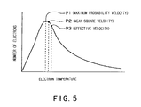
- the electron temperature is 3 eV or below, the excessive decomposition of the source gas can be suppressed, and an insulating film having a molecular structure effectively utilizing the characteristics of the source gas, such as an insulating film having a small relative dielectric constant and excellent electric characteristics, can be deposited.
- the slots have a length between half the wavelength of the microwave at the side of the waveguide with respect to a part of the flat antenna member and half the wavelength of the microwave at the side of the plasma producing space with respect to a part of the flat antenna member.
- the plurality of slots are arranged on concentric circles having their centers at the center of the flat antenna member or on a spiral around the center of the flat antenna member.
- the microwave radiated from the flat antenna member is a circularly polarized wave or a linearly polarized wave.
- the insulating film to be deposited on the substrate is a fluorine-containing carbon film.
- a plasma-assisted deposition system in a preferred embodiment according to the present invention will be described with reference to Figs. 1 to 7.
- the plasma-assisted deposition system is a CVD system (chemical vapor deposition system) using a radial line slot antenna for producing a plasma.
- a processing vessel (a vessel forming a vacuum chamber) 1 has a generally cylindrical shape.
- the side wall and the bottom wall of the processing vessel 1 are made of, for example, an Al-containing stainless steel.
- the inside surfaces of the processing vessel 1 is coated with a protective film of aluminum oxide.
- the processing vessel 1 has an open upper end.
- a first gas discharge head 2 substantially circular in a plane is placed in the open upper end of the processing vessel 1 opposite to the support table 11.
- a sealing member, not shown, such as an O ring, is placed between the upper end of the processing vessel 1 and the first gas discharge head 2.
- the first gas discharge head 2 is made of, for example, Al 2 O 3 and is provided many first gas discharge holes 21 opening in a surface thereof facing the support table 11.
- a gas passage 22 is formed in the gas discharge head 2 so as to connect to the first gas discharge holes 21.
- a first gas supply line 23 has one end connected to the gas passage 22 and the other end connected to a plasma gas source 24 for supplying a plasma gas, such as Ar gas or Kr gas and a hydrogen gas source 25 for supplying H 2 gas.
- a second gas discharge head 3 is disposed between the support table 11 and the first gas discharge head 2 in the processing vessel 1 so as to divide a space between the support table 11 and the first gas discharge head 2 into upper and lower spaces.
- the second gas discharge head 3 has, for example, a flat, substantially circular shape and is made of a conducting material, such as a Mg-containing Al alloy or an Al-containing stainless steel.
- the second gas discharge head 3 is provided in its surface facing the support table 11 with many second gas discharge holes 31.
- Gas passages 32 are formed, for example, in a grid inside the second gas discharge head 3 as shown in Fig. 2.
- the second gas discharge holes 31 communicate with the gas passages 32.
- the gas passages 32 are connected to one end of a second gas supply line 33.
- the second gas supply line 33 connects the second gas discharge head 3 to a source gas source 35 that supplies a source gas containing fluorine and carbon, such as C 5 F 8 .
- the second gas supply line 33 carries the source gas into the gas passages 32.
- the source gas is discharged through the gas discharge holes 31 into the lower space under the second gas discharge head 3 to distribute the source gas uniformly in the lower space.
- indicated at V1 to V3 are valves and at 101 to 103 are flow regulators.
- An antenna 4 is placed in close contact with the upper surface of the cover plate 13.
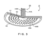
- the antenna 4 has an antenna body 41 of a flat, circular shape having an open lower end, and a circular, flat antenna member 42 provided with many slots (slot plate).
- the flat antenna member 42 is fitted in a recess formed in the open lower end of the antenna body 41.
- the antenna body 41 and the flat antenna member 42 are made of a conducting material.
- the antenna body 41 and the flat antenna member 42 constitute a flat, hollow circular waveguide.
- a lagging plate 43 made of a low-loss dielectric material, such as Al 2 O 3 , SiO 2 or Si 3 N 4 is sandwiched between the antenna body 41 and the flat antenna member 42.
- the lagging plate 43 shortens the wavelength of a microwave to shorten the wavelength in the waveguide.
- the antenna body 41, the flat antenna member 42 and the lagging plate 43 constitute a radial line slot antenna.
- the flat antenna member 42 is a copper plate of a thickness, for example, on the order of 1 mm. As shown in Figs. 3 and 4, the flat antenna member 42 is provided with many slots 46 for generating, for example, a circularly polarized wave.
- the slot 46 is a pair of slot 46a and slot 46b combined in T-shaped slot set so that the slots 46a and 46b are spaced a short distance apart.
- the T-shaped slot sets are arranged on concentric circles or a spiral. Since the slots 46a are perpendicular to their corresponding slots 46b, the antenna 4 radiates a circularly polarized wave having two perpendicularly intersecting wave components.
- the T-shaped slot sets each consisting of the slots 46a and 46b are arranged at intervals corresponding to the wavelength of the microwave compressed by the lagging plate 43 on concentric circles having their centers at the center of the flat antenna member 42 or a spiral around the center of the flat antenna member 42. Therefore, the flat antenna member 42 radiates a substantially plane microwave.
- the slots 46a and 46b are formed in a length L1 between half the wavelength of the microwave on the side of the waveguide 44 with respect to the flat antenna 42 and half the wavelength of the microwave on the side of a plasma producing space with respect to the flat antenna 42; that is the length L1 of the slots 46a and 46b is not longer than half the wavelength of the microwave on the side of the coaxial waveguide 44 with respect to the flat antenna 42 and longer than the wavelength of the microwave on the side of the plasma producing space, i.e., a space in the processing vessel 2, with respect to the antenna member 42.
- the microwave is able to propagate through the slots 46 into the plasma producing space and unable to propagate back from the plasma producing space into the coaxial waveguide 44.
- the distance L2 between the slot 46 on an inner circle and the slot 46 on an outer circle adjacent to the inner circle is, for example, equal to half the wavelength of the microwave on the side of the coaxial waveguide 44
- a film deposition method to be carried out by this plasma-assisted deposition system will be described by way of example.
- a wafer W namely, a substrate, provided with aluminum wiring lines on a surface thereof is carried through the gate valve into the processing vessel 1.
- the wafer W is placed on the support table 11.
- the processing vessel 1 is evacuated to a predetermined vacuum.
- a plasma gas such as Ar gas
- a source gas such as C 5 F 8 gas
- the interior of the processing vessel 1 is kept at a precess pressure of, for example, 13.3 Pa and the support table 11 is heated to a surface temperature of 350°C.
- the plasma-assisted deposition system in this embodiment forms the insulating film by plasma having the high electron density and a low electron temperature.
- the CF film thus formed has satisfactory electric characteristics including a small relative dielectric constant and capability of suppressing leakage current. It is inferred that such a CF film having satisfactory electric characteristics can be formed because all the cyclic bonds of C 5 F 8 gas, namely, a source gas, are not broken by excessive decomposed, only some of the cyclic bonds of C 5 F 8 gas are broken, and the broken C 5 F 8 molecules link together to form a three-dimensional structure of long CF chains.
- the CF film has molecular bonds intrinsic to the composition of the source gas.
- the CF film has excellent mechanical characteristics including high strength and high stress resistance, and excellent chemical characteristics including high water resistance. Since the plasma keeps a high electron density, the deposition rate will not decrease a level unsuitable for a mass production process.
- a source gas other than C 5 F 8 gas may be used for forming the CF film.
- Possible source gases are, for example, C 3 F 6 gas, C 4 F 6 gas and C 4 F 8 gas.
- the insulating film to be formed by the present invention is not limited to the CF film; the insulating film may be a SiOF film, namely, a film of a compound of silicon, oxygen and fluorine. Those insulating films, other than the CF film, having excellent electric characteristics and molecular bonds intrinsic to the composition of the source gas can be formed.
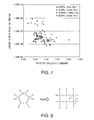
- blank squares indicate data on the CF films formed by using C 3 F 6 gas
- blank triangles indicate data on the CF films formed by using C 4 F 6 gas
- solid squares indicate data on the CF films formed by using C 4 F 8 gas
- blank rhombuses indicate data on the CF films formed by using C 5 F 8 gas.
- Electron temperature was preliminarily measured in a space between the source gas discharge holes and the wafer with a Langmuir probe. Electron temperature defined by mean square velocity was in the range of 1.1 to 2.0 eV. Since the process pressure is in the low process pressure range of 6.65 to 19.95 Pa (50 to 150 mTorr), electron density was on the order of 10 12 electrons per cubic centimeter. Electron density was confirmed by measurement using a Langmuir probe.
- Ar gas plasma Ar gas activated by plasma
- Ar gas plasma Ar gas activated by plasma
- the source gas plasma was used instead of the source gas plasma and measured the electron temperature and the electron density of the plasma with a Langmuir probe.
- Ar gas was used to determine electron temperature and electron density because there is the possibility that a CF gas corrodes the Langmuir probe. Values of electron temperature and electron density are substantially the same for different gases and hence there is no problem in the method of evaluation.
- Blank circles indicate data on CF films formed by the ECR plasma deposition system mentioned in Patent document 1 using C 5 F 8 gas and a plasma having an electron temperature in the range of 5 to 6 eV.
- An excellent interlayer insulation film must have a small relative dielectric constant and must be permitting only a low leakage current.
- the inventors of the present invention intend to provide interlayer insulation films having a relative dielectric constant of 2.2 or below and permitting a leakage current of 10 -8 A/cm 2 or below.
- the CF film has a large relative dielectric constant of 2.5 or above and permits a high leakage current of 10 -7 A/cm 2 when the electron temperature is higher than 5 eV.
- the large relative dielectric constant and the high leakage current are outside desired ranges.
- the electron temperature is 2 eV or below, the CF film has a small relative dielectric constant or permits only a low leakage current, or the small relative dielectric constant and the low leakage current. And characteristics of CF films are near the desired ranges.
- C 5 F 8 gas when used, data on the CF film lies near the desired ranges and it is inferred that CF bonds of C 5 F 8 gas are properly broken, the broken C 5 F 8 molecules link together to form a three-dimensional structure of long CF chains and the CF film is an insulating film having a small relative dielectric constant and permitting only a low leakage current.
- the electron temperature is higher than 5 eV, C 5 F 8 gas is completely decomposed and desired chain structure cannot be formed.
- CF films were formed under various process conditions by the plasma-assisted deposition system shown in Fig. 1 using C 5 F 8 gas as a source gas for pressures of processing atmosphere (process pressures) of 6.65 Pa (50 mTorr), 13.3 Pa (100 mTorr), 19.95 Pa (150 mTorr) and 26.6 Pa (200 mTorr).
- process pressures 6.65 Pa (50 mTorr), 13.3 Pa (100 mTorr), 19.95 Pa (150 mTorr) and 26.6 Pa (200 mTorr).
- the relative dielectric constants of the CF films and leakage currents flowed through the CF films were measured.
- Fig. 7 shows the measured results. In Fig. 7, leakage current is represented on the vertical axis and relative dielectric constant is represented on the horizontal axis.
- the process conditions are the distance between the second gas discharge head 3 and the wafer (Fig. 1), high-frequency power, the flow rate of Ar gas, the flow rate of the source gas and the temperature of the wafer.
- CF films were deposited by using various combinations of the process conditions for a fixed process pressure.
Landscapes
- Chemical & Material Sciences (AREA)
- Engineering & Computer Science (AREA)
- Physics & Mathematics (AREA)
- Plasma & Fusion (AREA)
- Analytical Chemistry (AREA)
- Chemical Kinetics & Catalysis (AREA)
- General Chemical & Material Sciences (AREA)
- Materials Engineering (AREA)
- Mechanical Engineering (AREA)
- Metallurgy (AREA)
- Organic Chemistry (AREA)
- Chemical Vapour Deposition (AREA)
- Formation Of Insulating Films (AREA)
Abstract
Description
Claims (14)
- A plasma-assisted deposition method for forming an insulating film on a substrate placed on a support device in an airtight processing vessel by activating a source gas by a plasma characterized in that a plasma producing space extending between source gas supply openings and a surface of the substrate has an electron temperature of 3 eV or below in terms of mean square velocity and an electron density of 5×10¹¹ electrons per cubic centimeter or above.
- The plasma-assisted deposition method according to claim 1, wherein a microwave is guided to a flat antenna member disposed opposite to the support device by a waveguide, and the microwave is radiated from a plurality of slots formed in a circumferential arrangement in the flat antenna member to activate the source gas by the energy of the microwave.
- The plasma-assisted deposition method according to claim 2, wherein the slots have a length between half the wavelength of the microwave at the side of the waveguide with respect to the flat antenna member and half the wavelength of the microwave at the side of the plasma producing space with respect to the flat antenna member.
- The plasma-assisted deposition method according to claim 2 or 3, wherein the plurality of slots are arranged on concentric circles having their centers at the center of the flat antenna member or on a spiral around the center of the flat antenna member.
- The plasma-assisted deposition method according to any one of claims 2 to 4, wherein the microwave radiated from the flat antenna member is a circularly polarized wave or a linearly polarized wave.
- The plasma-assisted deposition method according to any one of claims 1 to 5, wherein the pressure of a processing atmosphere is 19.95 Pa or below.
- The plasma-assisted deposition method according to any one of claims 1 to 6, wherein the insulating film to be deposited on the substrate is a fluorine-containing carbon film.
- The plasma-assisted deposition method according to claim 7, wherein the source gas is C5F8 gas.
- A plasma-assisted deposition system comprising:characterized in that a plasma producing space extending between source gas supply openings and a surface of the substrate has an electron temperature of 3 eV or below in terms of mean square velocity and an electron density of 5×10¹¹ electrons per cubic centimeter or above.an airtight processing vessel internally provided with a support device for supporting a substrate thereon;a source gas supply system for supplying a source gas for forming an insulating film on the substrate into the processing vessel;a microwave generator for generating a microwave for activating the source gas to produce a plasma;a waveguide for guiding the microwave generated by the microwave generator into the processing vessel; anda flat antenna member provided with a plurality of slots formed therein in a circumferential arrangement;
- The plasma-assisted deposition system according to claim 9, wherein the slots have a length between half the wavelength of the microwave at the side of the waveguide with respect to a part of the flat antenna member and half the wavelength of the microwave at the side of the plasma producing space with respect to a part of the flat antenna member.
- The plasma-assisted deposition system according to claim 10, wherein the plurality of slots are arranged on concentric circles having their centers at the center of the flat antenna member or on a spiral around the center of the flat antenna member.
- The plasma-assisted deposition system according to any one of claims 9 to 11, wherein the microwave radiated from the flat antenna member is a circularly polarized wave or a linearly polarized wave.
- The plasma-assisted deposition system according to any one of claims 9 to 12, wherein the insulating film to be deposited on the substrate is a fluorine-containing carbon film.
- The plasma-assisted deposition system according to claim 13, wherein the source gas is C5F8 gas.
Applications Claiming Priority (5)
| Application Number | Priority Date | Filing Date | Title |
|---|---|---|---|
| JP2003083292 | 2003-03-25 | ||
| JP2003083292 | 2003-03-25 | ||
| JP2004076958 | 2004-03-17 | ||
| JP2004076958A JP4369264B2 (en) | 2003-03-25 | 2004-03-17 | Plasma deposition method |
| PCT/JP2004/004070 WO2004086483A1 (en) | 2003-03-25 | 2004-03-24 | Plasma film-forming method and plasma film-forming apparatus |
Publications (2)
| Publication Number | Publication Date |
|---|---|
| EP1610369A1 true EP1610369A1 (en) | 2005-12-28 |
| EP1610369A4 EP1610369A4 (en) | 2007-03-07 |
Family
ID=33100373
Family Applications (1)
| Application Number | Title | Priority Date | Filing Date |
|---|---|---|---|
| EP04722947A Withdrawn EP1610369A4 (en) | 2003-03-25 | 2004-03-24 | PLASMA FILM FORMING METHOD AND PLASMA FILM FORMING APPARATUS |
Country Status (6)
| Country | Link |
|---|---|
| US (1) | US20060251828A1 (en) |
| EP (1) | EP1610369A4 (en) |
| JP (1) | JP4369264B2 (en) |
| KR (1) | KR100767492B1 (en) |
| TW (1) | TW200423213A (en) |
| WO (1) | WO2004086483A1 (en) |
Families Citing this family (20)
| Publication number | Priority date | Publication date | Assignee | Title |
|---|---|---|---|---|
| EP1115147A4 (en) * | 1999-05-26 | 2007-05-02 | Tadahiro Ohmi | PLASMA TREATMENT DEVICE |
| JP2006135303A (en) * | 2004-10-05 | 2006-05-25 | Tokyo Electron Ltd | Plasma film forming method, plasma film forming apparatus, and storage medium used in plasma film forming apparatus |
| JP4664119B2 (en) | 2005-05-17 | 2011-04-06 | 東京エレクトロン株式会社 | Plasma processing equipment |
| JP5162108B2 (en) | 2005-10-28 | 2013-03-13 | 日新電機株式会社 | Plasma generating method and apparatus, and plasma processing apparatus |
| EP1997620B1 (en) * | 2006-03-17 | 2016-06-15 | National Institute of Advanced Industrial Science and Technology | Laminated body and carbon film deposition method |
| US8006640B2 (en) * | 2006-03-27 | 2011-08-30 | Tokyo Electron Limited | Plasma processing apparatus and plasma processing method |
| JP5082411B2 (en) * | 2006-12-01 | 2012-11-28 | 東京エレクトロン株式会社 | Deposition method |
| KR100898128B1 (en) * | 2007-07-30 | 2009-05-18 | 한국생산기술연구원 | Micropattern manufacturing method using inkjet printing and plasma surface treatment |
| JP2009088267A (en) * | 2007-09-28 | 2009-04-23 | Tokyo Electron Ltd | Film forming method, film forming apparatus, storage medium, and semiconductor device |
| WO2010129901A2 (en) | 2009-05-08 | 2010-11-11 | Vandermeulen Peter F | Methods and systems for plasma deposition and treatment |
| JP5514310B2 (en) * | 2010-06-28 | 2014-06-04 | 東京エレクトロン株式会社 | Plasma processing method |
| US9530621B2 (en) * | 2014-05-28 | 2016-12-27 | Tokyo Electron Limited | Integrated induction coil and microwave antenna as an all-planar source |
| JP2019500495A (en) * | 2015-12-02 | 2019-01-10 | ビーエーエスエフ ソシエタス・ヨーロピアBasf Se | Method for producing thin inorganic film |
| JP6664047B2 (en) * | 2016-03-31 | 2020-03-13 | 株式会社昭和真空 | Film forming apparatus and film forming method |
| JP6899693B2 (en) * | 2017-04-14 | 2021-07-07 | 東京エレクトロン株式会社 | Plasma processing equipment and control method |
| US10546724B2 (en) * | 2017-05-10 | 2020-01-28 | Mks Instruments, Inc. | Pulsed, bidirectional radio frequency source/load |
| US10861667B2 (en) | 2017-06-27 | 2020-12-08 | Peter F. Vandermeulen | Methods and systems for plasma deposition and treatment |
| CN111033689B (en) | 2017-06-27 | 2023-07-28 | 彼得·F·范德莫伊伦 | Methods and systems for plasma deposition and processing |
| US12318499B2 (en) | 2020-03-13 | 2025-06-03 | Peter F. Vandermeulen | Methods and systems for medical plasma treatment and generation of plasma activated media |
| KR102864349B1 (en) * | 2022-06-21 | 2025-09-24 | 주식회사 히타치하이테크 | Plasma treatment device and heating device |
Family Cites Families (16)
| Publication number | Priority date | Publication date | Assignee | Title |
|---|---|---|---|---|
| US5134965A (en) * | 1989-06-16 | 1992-08-04 | Hitachi, Ltd. | Processing apparatus and method for plasma processing |
| US5698036A (en) * | 1995-05-26 | 1997-12-16 | Tokyo Electron Limited | Plasma processing apparatus |
| US5803975A (en) * | 1996-03-01 | 1998-09-08 | Canon Kabushiki Kaisha | Microwave plasma processing apparatus and method therefor |
| WO1998033362A1 (en) * | 1997-01-29 | 1998-07-30 | Tadahiro Ohmi | Plasma device |
| US5800621A (en) * | 1997-02-10 | 1998-09-01 | Applied Materials, Inc. | Plasma source for HDP-CVD chamber |
| TW376547B (en) * | 1997-03-27 | 1999-12-11 | Matsushita Electric Industrial Co Ltd | Method and apparatus for plasma processing |
| KR100382388B1 (en) * | 1997-11-27 | 2003-05-09 | 동경 엘렉트론 주식회사 | Method for forming plasma films |
| JP3515347B2 (en) * | 1997-11-27 | 2004-04-05 | 東京エレクトロン株式会社 | Semiconductor device manufacturing method and semiconductor device |
| JP3189781B2 (en) * | 1998-04-08 | 2001-07-16 | 日本電気株式会社 | Method for manufacturing semiconductor device |
| JP4361625B2 (en) * | 1998-10-05 | 2009-11-11 | 東京エレクトロン株式会社 | Semiconductor device and manufacturing method thereof |
| US6870123B2 (en) * | 1998-10-29 | 2005-03-22 | Canon Kabushiki Kaisha | Microwave applicator, plasma processing apparatus having same, and plasma processing method |
| JP2001308071A (en) * | 2000-04-26 | 2001-11-02 | Canon Inc | Plasma processing apparatus and plasma processing method using waveguide having E-plane branch |
| US6652709B1 (en) * | 1999-11-02 | 2003-11-25 | Canon Kabushiki Kaisha | Plasma processing apparatus having circular waveguide, and plasma processing method |
| JP4478352B2 (en) * | 2000-03-29 | 2010-06-09 | キヤノン株式会社 | Plasma processing apparatus, plasma processing method, and structure manufacturing method |
| JP2002220668A (en) * | 2000-11-08 | 2002-08-09 | Daikin Ind Ltd | Film forming gas and plasma film forming method |
| JP5010781B2 (en) * | 2001-03-28 | 2012-08-29 | 忠弘 大見 | Plasma processing equipment |
-
2004
- 2004-03-17 JP JP2004076958A patent/JP4369264B2/en not_active Expired - Fee Related
- 2004-03-24 US US10/549,859 patent/US20060251828A1/en not_active Abandoned
- 2004-03-24 TW TW093107994A patent/TW200423213A/en not_active IP Right Cessation
- 2004-03-24 EP EP04722947A patent/EP1610369A4/en not_active Withdrawn
- 2004-03-24 WO PCT/JP2004/004070 patent/WO2004086483A1/en not_active Ceased
- 2004-03-24 KR KR1020057017916A patent/KR100767492B1/en not_active Expired - Fee Related
Also Published As
| Publication number | Publication date |
|---|---|
| WO2004086483A1 (en) | 2004-10-07 |
| JP2004311975A (en) | 2004-11-04 |
| EP1610369A4 (en) | 2007-03-07 |
| TW200423213A (en) | 2004-11-01 |
| KR20050117576A (en) | 2005-12-14 |
| KR100767492B1 (en) | 2007-10-17 |
| US20060251828A1 (en) | 2006-11-09 |
| JP4369264B2 (en) | 2009-11-18 |
| TWI335610B (en) | 2011-01-01 |
Similar Documents
| Publication | Publication Date | Title |
|---|---|---|
| EP1610369A1 (en) | Plasma film-forming method and plasma film-forming apparatus | |
| US8753527B2 (en) | Plasma etching method and plasma etching apparatus | |
| US6497783B1 (en) | Plasma processing apparatus provided with microwave applicator having annular waveguide and processing method | |
| US6870123B2 (en) | Microwave applicator, plasma processing apparatus having same, and plasma processing method | |
| US5897713A (en) | Plasma generating apparatus | |
| US7138767B2 (en) | Surface wave plasma processing system and method of using | |
| US6372084B2 (en) | Plasma processing apparatus with a dielectric plate having a thickness based on a wavelength of a microwave introduced into a process chamber through the dielectric plate | |
| JP2925535B2 (en) | Microwave supplier having annular waveguide, plasma processing apparatus and processing method having the same | |
| US20070254113A1 (en) | Plasma processing apparatus having an evacuating arrangement to evacuate gas from gas-introducing part of a process chamber | |
| KR20200058298A (en) | Scaled liner layer for isolation structure | |
| TW200818269A (en) | Method of forming film, film forming device and memory medium as well as semiconductor device | |
| WO2006038976A2 (en) | Plasma processing system for treating a substrate | |
| SG11202112769WA (en) | Substrate processing chamber | |
| EP1895565A1 (en) | Plasma processing apparatus and method | |
| US7584714B2 (en) | Method and system for improving coupling between a surface wave plasma source and a plasma space | |
| US20080311313A1 (en) | Film Forming Method and Film Forming Apparatus | |
| JP4478352B2 (en) | Plasma processing apparatus, plasma processing method, and structure manufacturing method | |
| JP3530788B2 (en) | Microwave supplier, plasma processing apparatus and processing method | |
| KR100425658B1 (en) | Microwave applicator, plasma processing apparatus having same, and plasma processing method | |
| JPH11329792A (en) | Microwave feeder | |
| US12424422B2 (en) | Plasma processing apparatus and semiconductor device manufacturing method | |
| CN100527365C (en) | Plasma film forming method and plasma film forming device | |
| JP2019062045A (en) | Planarization method for boron-based film and formation method for boron-based film |
Legal Events
| Date | Code | Title | Description |
|---|---|---|---|
| PUAI | Public reference made under article 153(3) epc to a published international application that has entered the european phase |
Free format text: ORIGINAL CODE: 0009012 |
|
| 17P | Request for examination filed |
Effective date: 20050927 |
|
| AK | Designated contracting states |
Kind code of ref document: A1 Designated state(s): AT BE BG CH CY CZ DE DK EE ES FI FR GB GR HU IE IT LI LU MC NL PL PT RO SE SI SK TR |
|
| AX | Request for extension of the european patent |
Extension state: AL LT LV MK |
|
| DAX | Request for extension of the european patent (deleted) | ||
| RBV | Designated contracting states (corrected) |
Designated state(s): DE FR GB IT NL |
|
| A4 | Supplementary search report drawn up and despatched |
Effective date: 20070206 |
|
| RIN1 | Information on inventor provided before grant (corrected) |
Inventor name: NISHIZAWA, KENICHI Inventor name: TERAI, YASUHIRO Inventor name: ASANO, AKIRA Inventor name: KAWAMURA, KOHEIC/O TOKYO ELECTRON LIMITED Inventor name: KOBAYASHI, YASUOC/O TOKYO ELECTRON LIMITED |
|
| 17Q | First examination report despatched |
Effective date: 20070813 |
|
| RIC1 | Information provided on ipc code assigned before grant |
Ipc: H01J 37/32 20060101ALI20131217BHEP Ipc: H01L 21/02 20060101ALI20131217BHEP Ipc: C23C 16/511 20060101AFI20131217BHEP Ipc: H01L 21/312 20060101ALI20131217BHEP |
|
| GRAP | Despatch of communication of intention to grant a patent |
Free format text: ORIGINAL CODE: EPIDOSNIGR1 |
|
| INTG | Intention to grant announced |
Effective date: 20140416 |
|
| STAA | Information on the status of an ep patent application or granted ep patent |
Free format text: STATUS: THE APPLICATION IS DEEMED TO BE WITHDRAWN |
|
| 18D | Application deemed to be withdrawn |
Effective date: 20140827 |