EP1610349A2 - Inductance device - Google Patents

Inductance device Download PDF

Info

Publication number
EP1610349A2
EP1610349A2 EP05006868A EP05006868A EP1610349A2 EP 1610349 A2 EP1610349 A2 EP 1610349A2 EP 05006868 A EP05006868 A EP 05006868A EP 05006868 A EP05006868 A EP 05006868A EP 1610349 A2 EP1610349 A2 EP 1610349A2
Authority
EP
European Patent Office
Prior art keywords
aforementioned
magnetic
winding section
magnetic flux
inductance device
Prior art date
Legal status (The legal status is an assumption and is not a legal conclusion. Google has not performed a legal analysis and makes no representation as to the accuracy of the status listed.)
Granted
Application number
EP05006868A
Other languages
German (de)
French (fr)
Other versions
EP1610349A3 (en
EP1610349B1 (en
Inventor
Mitsugu c/o Sumida Corporation Kawarai
Current Assignee (The listed assignees may be inaccurate. Google has not performed a legal analysis and makes no representation or warranty as to the accuracy of the list.)
Sumida Corp
Original Assignee
Sumida Corp
Priority date (The priority date is an assumption and is not a legal conclusion. Google has not performed a legal analysis and makes no representation as to the accuracy of the date listed.)
Filing date
Publication date
Application filed by Sumida Corp filed Critical Sumida Corp
Publication of EP1610349A2 publication Critical patent/EP1610349A2/en
Publication of EP1610349A3 publication Critical patent/EP1610349A3/en
Application granted granted Critical
Publication of EP1610349B1 publication Critical patent/EP1610349B1/en
Anticipated expiration legal-status Critical
Expired - Lifetime legal-status Critical Current

Links

Images

Classifications

    • HELECTRICITY
    • H01ELECTRIC ELEMENTS
    • H01FMAGNETS; INDUCTANCES; TRANSFORMERS; SELECTION OF MATERIALS FOR THEIR MAGNETIC PROPERTIES
    • H01F17/00Fixed inductances of the signal type
    • H01F17/0006Printed inductances
    • H01F17/0033Printed inductances with the coil helically wound around a magnetic core
    • HELECTRICITY
    • H01ELECTRIC ELEMENTS
    • H01FMAGNETS; INDUCTANCES; TRANSFORMERS; SELECTION OF MATERIALS FOR THEIR MAGNETIC PROPERTIES
    • H01F17/00Fixed inductances of the signal type
    • H01F17/0006Printed inductances
    • H01F17/0013Printed inductances with stacked layers
    • HELECTRICITY
    • H01ELECTRIC ELEMENTS
    • H01FMAGNETS; INDUCTANCES; TRANSFORMERS; SELECTION OF MATERIALS FOR THEIR MAGNETIC PROPERTIES
    • H01F17/00Fixed inductances of the signal type
    • H01F17/04Fixed inductances of the signal type with magnetic core
    • H01F17/045Fixed inductances of the signal type with magnetic core with core of cylindric geometry and coil wound along its longitudinal axis, i.e. rod or drum core
    • HELECTRICITY
    • H01ELECTRIC ELEMENTS
    • H01FMAGNETS; INDUCTANCES; TRANSFORMERS; SELECTION OF MATERIALS FOR THEIR MAGNETIC PROPERTIES
    • H01F27/00Details of transformers or inductances, in general
    • H01F27/24Magnetic cores
    • H01F27/255Magnetic cores made from particles
    • HELECTRICITY
    • H01ELECTRIC ELEMENTS
    • H01FMAGNETS; INDUCTANCES; TRANSFORMERS; SELECTION OF MATERIALS FOR THEIR MAGNETIC PROPERTIES
    • H01F27/00Details of transformers or inductances, in general
    • H01F27/28Coils; Windings; Conductive connections
    • H01F27/2804Printed windings
    • HELECTRICITY
    • H01ELECTRIC ELEMENTS
    • H01FMAGNETS; INDUCTANCES; TRANSFORMERS; SELECTION OF MATERIALS FOR THEIR MAGNETIC PROPERTIES
    • H01F3/00Cores, Yokes, or armatures
    • H01F3/10Composite arrangements of magnetic circuits
    • H01F3/14Constrictions; Gaps, e.g. air-gaps

Definitions

  • patent literature associated with the present invention includes the gazette of Japanese Kokai Publication 2001-267129 as the first and the gazette of Japanese Kokai Publication Hei-10-335144 as the second.
  • the inductance device pursuant to the present invention is provided with a ring-shaped coil having an n winding section in which the number of windings is n and an n + 1 winding section in which the number of windings is n + 1, magnetic circuit material mounted within and without the ring of aforementioned coil through which magnetic flux is passed to form a magnetic circuit, and a magnetic gap that blocks either the magnetic flux that was formed so as to surround aforementioned n winding section or the magnetic flux that was formed so as to surround aforementioned n + 1 winding section.
  • the inductance device pursuant to the present invention is provided with a ring-shaped coil having an n winding section in which the number of windings is n and an n + 1 winding section in which the number of windings is n + 1, magnetic circuit material mounted within and without the ring of aforementioned coil through which magnetic flux is passed to form a magnetic circuit, a first magnetic gap that blocks either the magnetic flux that was formed so as to surround aforementioned n winding section or the magnetic flux that was formed so as to surround aforementioned n + 1 winding section, and a second magnetic gap that is narrower than the first magnetic gap that blocks aforementioned magnetic flux in a direction orthogonal to the axial direction of aforementioned ring.
  • aforementioned soft magnetic ceramic member that is mounted within and without the ring of aforementioned coil to comprise magnetic circuit material through which magnetic flux is passed to form a magnetic circuit, and a magnetic gap that is mounted that blocks either the magnetic flux that was formed so as to surround aforementioned n winding section or the magnetic flux that was formed so as to surround aforementioned n + 1 winding section.
  • aforementioned soft magnetic ceramic member that is mounted within and without the ring of aforementioned coil to comprise magnetic circuit material through which magnetic flux is passed to form a magnetic circuit, a first magnetic gap that blocks either the magnetic flux that was formed so as to surround aforementioned n winding section or the magnetic flux that was formed so as to surround aforementioned n + 1 winding section, and a second magnetic gap that is narrower than the first magnetic gap that blocks aforementioned magnetic flux in a direction orthogonal to the axial direction of aforementioned ring.
  • Winding origin 33 and winding terminus 34 of coil 3 extend from the ring-shaped section to the sides of electrodes 2, 2 where they connect to electrode 2.
  • n winding section 31 in coil 3 contains a section parallel to n+1 winding section 32.
  • the conductor comprising coil 3 with an exposed side is formed on the side wall of inductance device 1, and insulating resin 4 is applied to this exposed section.
  • the ring center in coil 3 and the exterior of n+1 winding section 32 are formed from magnetic material 5 which is magnetic circuit material.
  • Nonmagnetic material 6 is mounted so that conductor pattern 3a of the coil is interposed.
  • nonmagnetic material 6 is mounted above and below n winding section 31 so as to be thicker than the separation between conductor patterns 3a, 3a.
  • nonmagnetic material 6 that covers the region corresponding to one turn of coil 3 and the region that covers the terminus which extends to the electrode (region corresponding to 1.5 turns) is printed, as shown in ( Figure 5 (c1)).
  • a window is mounted in the section of nonmagnetic material 6 corresponding to the terminus of conductor pattern 3a shown in Figure 5 (b1), and nonmagnetic material 6 is not applied.
  • the exterior of the final straight part in conductor pattern 3a having a three-sided box (shape) as shown in Figure 5 (b1) remains exposed in this state.
  • insulating resin 4 is applied to this exposed section.
  • a paste comprising conducting powder primarily of silver with synthetic resin binder is used as conductor pattern 3a
  • a paste comprising ferrite soft magnetic powder (for example, Ni-Cu-Zn ferrite) with synthetic resin binder is used as magnetic material of the magnetic layer comprising magnetic material 5
  • a paste comprising nonmagnetic ceramic powder (for example, Ni-Cu ferrite or glass ceramic) with synthetic resin binder is used as nonmagnetic material 6.
  • a magnetic layer comprising magnetic material 5 that is laid on top of this multilayered construct is oriented in place, press-laminated and concurrently sintered to complete construction.
  • a structure having a section with two turns (two windings) and a section with one turn (one winding) so as to have 1.5 turns overall is shown to have poor direct-current superimposition characteristics and a low inductance value. Further improvement in the direct-current superimposition characteristics by mounting second magnetic gap 7 was attempted in a working example.
  • Figure 8 is an A-A profile of inductance device 1 in this working example while Figure 9 is a B-B profile.
  • the conductor comprising coil 3 with an exposed side is formed, and insulating resin 4 is applied to this exposed section, but in this working example, nonmagnetic material 6 is disposed on the section covered by aforementioned insulating resin 4, and the top, bottom and outside of n winding section 31 are surrounded by nonmagnetic material 6 so as to form a magnetic gap that blocks the magnetic flux from forming so as to surround n winding section 31.
  • the ring center in coil 3A and the exterior of n+1 winding section 32 are formed from magnetic material 5 which is magnetic circuit material.
  • Nonmagnetic material 6 is mounted so that conductor pattern 3a of the coil is interposed.
  • nonmagnetic material 6 is mounted above and below n winding section 31 so as to be thicker than the separation between conductor patterns 3a, 3a in n+1 winding section 32.
  • a structure having a section with two turns (two windings) and a section with one turn (one winding) so as to have 1.5 turns overall is shown to have poor direct-current superimposition characteristics and a low inductance value. Further improvement in the direct-current superimposition characteristics by mounting second magnetic gap 7 was attempted in a working example.
  • Second magnetic gap 7 comprising nonmagnetic material that is narrower (thinner) than nonmagnetic material 6 that is mounted above and below n winding section 31 is mounted between the bottom-most conductor pattern 3a in n+1 winding section 32 and conductor pattern 3a thereabove, viewed from the bottom of conductor pattern 3a of n winding section 31.

Landscapes

  • Engineering & Computer Science (AREA)
  • Power Engineering (AREA)
  • Microelectronics & Electronic Packaging (AREA)
  • Chemical & Material Sciences (AREA)
  • Composite Materials (AREA)
  • Coils Or Transformers For Communication (AREA)
  • Coils Of Transformers For General Uses (AREA)

Abstract

The superimposition characteristics are improved in an inductance device pursuant to the present invention provided with coils having sections with different numbers of windings. The inductance device pursuant to the present invention is provided with a ring-shaped coil having n winding section 31 in which the number of windings is n and n+1 winding section 32 in which the number of windings is n + 1, magnetic circuit material mounted within and without the ring of aforementioned coil through which magnetic flux is passed to form a magnetic circuit, and a magnetic gap that blocks either the magnetic flux that was formed so as to surround aforementioned n winding section 31 or the magnetic flux that was formed so as to surround aforementioned n+1 winding section 32.

Description

Technical Field of Invention
The present invention concerns an inductance device having a ring-shaped coil.
Background Technology
A multilayered type of inductance device has the shape of a block-shaped parallelepiped, for example, with electrodes mounted on two opposing surfaces of the parallelepiped and terminal patterns extended to a coil within the block that are connected to aforementioned electrodes.
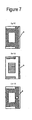
For this reason, aforementioned extended sections in a ring-shaped coil have a structure in which the number of windings (number of turns) is one turn greater than in other ring sections, as shown in Figure 4, for example.
When using an inductance device with such a structure, the magnetic field that is generated develops imbalance commensurate with the number of turns, and this is known to lower the direct-current superimposition characteristics.
The patent literature associated with the present invention that can be cited includes the gazette of Japanese Kokai Publication 2001-267129 as the first and the gazette of Japanese Kokai Publication Hei-10-335144 as the second.
Problems Solved by the Invention
The purpose of the present invention is to provide an inductance device with good direct-current superimposition characteristics in which the imbalance in the magnetic field that is generated is corrected by the provision of a section with a large number of turns and a section with a low number of turns to solve aforementioned problems.
Means of Solving the Problems
The inductance device pursuant to the present invention is provided with a ring-shaped coil having an n winding section in which the number of windings is n and an n + 1 winding section in which the number of windings is n + 1, magnetic circuit material mounted within and without the ring of aforementioned coil through which magnetic flux is passed to form a magnetic circuit, and a magnetic gap that blocks either the magnetic flux that was formed so as to surround aforementioned n winding section or the magnetic flux that was formed so as to surround aforementioned n + 1 winding section.
The inductance device pursuant to the present invention is provided with a ring-shaped coil having an n winding section in which the number of windings is n and an n + 1 winding section in which the number of windings is n + 1, magnetic circuit material mounted within and without the ring of aforementioned coil through which magnetic flux is passed to form a magnetic circuit, a first magnetic gap that blocks either the magnetic flux that was formed so as to surround aforementioned n winding section or the magnetic flux that was formed so as to surround aforementioned n + 1 winding section, and a second magnetic gap that is narrower than the first magnetic gap that blocks aforementioned magnetic flux in a direction orthogonal to the axial direction of aforementioned ring.
The inductance device pursuant to the present invention is a multilayered type of inductance device that is structured with a ring-shaped coil having an n winding section in which the number of windings is n and an n + 1 winding section in which the number of windings is n + 1, and with a soft magnetic ceramic member that is embedded within aforementioned coil, both of which are layered within the same device. It is provided with aforementioned soft magnetic ceramic member that is mounted within and without the ring of aforementioned coil to comprise magnetic circuit material through which magnetic flux is passed to form a magnetic circuit, and a magnetic gap that is mounted that blocks either the magnetic flux that was formed so as to surround aforementioned n winding section or the magnetic flux that was formed so as to surround aforementioned n + 1 winding section.
The inductance device pursuant to the present invention is a multilayered type of inductance device that is structured with a ring-shaped coil having an n winding section in which the number of windings is n and an n + 1 winding section in which the number of windings is n + 1, and with a soft magnetic ceramic member that is embedded within aforementioned coil, both of which are layered within the same device. It is provided with aforementioned soft magnetic ceramic member that is mounted within and without the ring of aforementioned coil to comprise magnetic circuit material through which magnetic flux is passed to form a magnetic circuit, a first magnetic gap that blocks either the magnetic flux that was formed so as to surround aforementioned n winding section or the magnetic flux that was formed so as to surround aforementioned n + 1 winding section, and a second magnetic gap that is narrower than the first magnetic gap that blocks aforementioned magnetic flux in a direction orthogonal to the axial direction of aforementioned ring.
The inductance device pursuant to the present invention is structured so that the first and second magnetic gaps that block aforementioned magnetic flux are made of nonmagnetic ceramic.
A magnetic gap that blocks the magnetic flux is formed since part of either aforementioned n winding section or aforementioned n+ 1 winding section is exposed outside of the block formed from magnetic circuit material in the inductance device pursuant to the present invention.
The inductance device pursuant to the present invention is characterized by coating aforementioned exposed section with insulating resin.
The number n in aforementioned n winding section and aforementioned n + 1 winding section in the inductance device pursuant to the present invention is not more than 4.
Effects of Invention
Improvement in the direction of balancing the imbalance in the magnetic flux that was formed is possible since either the magnetic flux that was formed so as to surround the n winding section or the magnetic flux that was formed so as to surround the n + 1 winding section is blocked in the inductance device having aforementioned structure, and the direct-current superimposition characteristics can be improved.
Brief Description of Drawings
  • Figure 1 is a general view of an inductance device in each working example of the present invention.
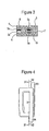
  • Figure 2 is an A-A profile of the inductance device in Figure 1 in the first working example.
  • Figure 3 is a B-B profile of the inductance device in Figure 1 in the first working example.
  • Figure 4 is an oblique view showing the coil used in the first and second working examples of the present invention.
  • Figure 5 is a diagram showing the production steps of the inductance device pursuant to the first working example of the present invention.
  • Figure 6 is a diagram showing the production steps of the inductance device pursuant to the first working example of the present invention.
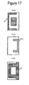
  • Figure 7 is a diagram showing the production steps of the inductance device pursuant to the first working example of the present invention.
  • Figure 8 is an A-A profile of the inductance device in Figure 1 in the second working example.
  • Figure 9 is a B-B profile of the inductance device in Figure 1 in the second working example.
  • Figure 10 is a diagram showing the production steps of the inductance device pursuant to the second working example of the present invention.
  • Figure 11 is a diagram showing the production steps of the inductance device pursuant to the second working example of the present invention.
  • Figure 12 is a diagram showing the production steps of the inductance device pursuant to the second working example of the present invention.
  • Figure 13 is an oblique view showing the coil used in the third and fourth working examples of the present invention.
  • Figure 14 is an A-A profile of the inductance device in Figure 1 in the third working example.
  • Figure 15 is a B-B profile of the inductance device in Figure 1 in the third working example.
  • Figure 16 is a diagram showing the production steps of the inductance device pursuant to the third working example of the present invention.
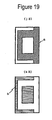
  • Figure 17 is a diagram showing the production steps of the inductance device pursuant to the third working example of the present invention.
  • Figure 18 is a diagram showing the production steps of the inductance device pursuant to the third working example of the present invention.
  • Figure 19 is a diagram showing the production steps of the inductance device pursuant to the third working example of the present invention.
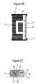
  • Figure 20 is an A-A profile of the inductance device in Figure 1 in the fourth working example.
  • Figure 21 is a B-B profile of the inductance device in Figure 1 in the fourth working example.
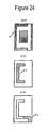
  • Figure 22 is a diagram showing the production steps of the inductance device pursuant to the fourth working example of the present invention.
  • Figure 23 is a diagram showing the production steps of the inductance device pursuant to the fourth working example of the present invention.
  • Figure 24 is a diagram showing the production steps of the inductance device pursuant to the fourth working example of the present invention.
  • Figure 25 is a diagram showing the production steps of the inductance device pursuant to the fourth working example of the present invention.
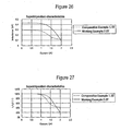
  • Figure 26 is a diagram showing the direct-current superimposition characteristics in this working example and in a comparative example.
  • Figure 27 is a diagram showing the ratios of the direct-current superimposition characteristics in this working example and in a comparative example.
  • Figure 28 is an A-A profile of the inductance device in Figure 1 in the fifth working example.
  • Figure 29 is a B-B profile of the inductance device in Figure 1 in the fifth working example.
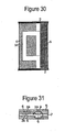
  • Figure 30 is an A-A profile of the inductance device in Figure 1 in the sixth working example.
  • Figure 31 is a B-B profile of the inductance device in Figure 1 in the sixth working example.
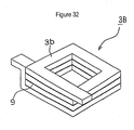
  • Figure 32 is an oblique view showing one example of a coil used in the seventh working example of the present invention.
  • Figure 33 is an oblique view showing one example of the case used when constructing an inductance device pursuant to the seventh working example using the coil shown in Figure 32.
  • Best Mode for Implementing Invention
    The objective of improving the direct-current superimposition characteristics by correcting the imbalance in the magnetic field that is generated in the section with a large number of turns and the section with a low number of turns is attained by a comparatively simple structure in which a magnetic gap that blocks the magnetic flux is mounted. Working examples of the inductance device pursuant to the present invention are explained with reference to the appended figures below. Identical structures in each diagram are given the same notation to avoid duplicate explanation.
    Working Example 1
    Figure 1 shows a general view of inductance device 1. Figure 2 is an A-A profile. Figure 3 is a B-B profile. Electrodes 2 are mounted on a pair of surfaces that face inductance device 1. Figure 4 shows isolated coil 3. In short, it has a square ring shape with n winding section 31 in which the number of windings is n and n+1 winding section 32 in which the number of windings is n + 1.
    Winding origin 33 and winding terminus 34 of coil 3 extend from the ring-shaped section to the sides of electrodes 2, 2 where they connect to electrode 2. n winding section 31 in coil 3 contains a section parallel to n+1 winding section 32. The conductor comprising coil 3 with an exposed side is formed on the side wall of inductance device 1, and insulating resin 4 is applied to this exposed section.
    The ring center in coil 3 and the exterior of n+1 winding section 32 are formed from magnetic material 5 which is magnetic circuit material. Nonmagnetic material 6 is mounted so that conductor pattern 3a of the coil is interposed. In particular, nonmagnetic material 6 is mounted above and below n winding section 31 so as to be thicker than the separation between conductor patterns 3a, 3a.
    Second magnetic gap 7 comprising nonmagnetic material that is narrower (thinner) than the first magnetic gap made of nonmagnetic material 6 that is mounted above and below n winding section 31 is mounted between the bottom-most conductor pattern 3a in n+1 winding section 32 and conductor pattern 3a thereabove, viewed from the bottom of conductor pattern 3a of n winding section 31.
    Inductance device 1 is constructed through the procedures shown in Figures 5 to 7. A magnetic layer is formed by superimposing a plurality of magnetic sheets, and nonmagnetic material 6 is thickly applied at the position where n winding section 31, which is over said magnetic layer, is disposed. Magnetic material 5 is mounted in the remaining regions so as to form a flat surface. Bar-shaped conductor pattern 3a, which is formed through printing with a mask, extends in linear shape from one edge on which is mounted electrode 2 and terminates 2/3 of the distance to the other end on this flat surface, as shown in Figure 5 (a1). Next, conductor pattern 3a with a three-sided box (shape) corresponding to 1/2 turn of coil 3 is formed by mask printing (Figure 5 (b1)).
    Next, nonmagnetic material 6 that covers the region corresponding to one turn of coil 3 and the region that covers the terminus which extends to the electrode (region corresponding to 1.5 turns) is printed, as shown in (Figure 5 (c1)). A window is mounted in the section of nonmagnetic material 6 corresponding to the terminus of conductor pattern 3a shown in Figure 5 (b1), and nonmagnetic material 6 is not applied. The exterior of the final straight part in conductor pattern 3a having a three-sided box (shape) as shown in Figure 5 (b1) remains exposed in this state.
    Next, as shown in Figure 6 (d1), magnetic material 5 is printed in regions excluding the region of nonmagnetic material 6 in Figure 5 (c1). Then, conductor pattern 3a is formed through printing by using a mask with an aperture at the region corresponding to 1/2 turn of the wire of coil 3 so as to match Figure 5 (b1), as shown in Figure 6 (e1). Bar-shaped conductor pattern 3a, which is formed through printing with a mask, extends in linear shape from the terminus of conductor pattern 3a in Figure 6 (e1) to the other end, as shown in Figure 6 (f1).
    Next, nonmagnetic material 6 that covers the region corresponding to one turn of coil 7 and the region that covers the terminus which extends to the electrode (region corresponding to 1.5 turns) is printed, as shown in Figure 7 (g1). Next, as shown in Figure 7 (h1), magnetic material 5 is printed in regions excluding the region of nonmagnetic material 6 in Figure 7 (g1). An inductance device for 1.5 turns worth is completed in aforementioned manner.
    To construct an inductance device for 1.5 turns worth + N (N is an integer) turns worth, nonmagnetic material 6 would be printed so as to cover the region corresponding to one turn of coil 3 and the region that covers the terminus which extends to the electrode (region corresponding to 1.5 turns), as shown in Figure 7 (f1'), instead of using the mask shown in Figure 6 (f1). In the region of nonmagnetic material 6, a window is mounted in the section of nonmagnetic material 6 corresponding to the terminus of conductor pattern 3a shown in Figure 6 (e1), and nonmagnetic material 6 is not applied. The sequence of procedures returns from the step shown in Figure 7 (f1') to the step shown in Figure 5 (b1), and the steps shown in Figure 5 (b1), Figure 5 (c1), Figure 6 (d1), Figure 6 (e1), Figure 7 (f1') are repeated.
    When second magnetic gap 7 is mounted, it has the same size as that of the surface of inductance device 1. A sheet of nonmagnetic material having the same window as the window mounted in nonmagnetic material 6 of Figure 7 (f1') is used. Second magnetic gap 7 can be mounted by using this sheet of nonmagnetic material instead of nonmagnetic material 6 from Figure 7 (f1').
    Since the side of the conductor comprising coil 3 is exposed in such a multilayered state, insulating resin 4 is applied to this exposed section. As noted above, a paste comprising conducting powder primarily of silver with synthetic resin binder is used as conductor pattern 3a, a paste comprising ferrite soft magnetic powder (for example, Ni-Cu-Zn ferrite) with synthetic resin binder is used as magnetic material of the magnetic layer comprising magnetic material 5, and a paste comprising nonmagnetic ceramic powder (for example, Ni-Cu ferrite or glass ceramic) with synthetic resin binder is used as nonmagnetic material 6. A magnetic layer comprising magnetic material 5 that is laid on top of this multilayered construct is oriented in place, press-laminated and concurrently sintered to complete construction.
    Nonmagnetic material 6 is mounted above and below n winding section 31 so as to be thicker than the separation between conductor patterns 3a, 3a, the conductor comprising coil 3 with an exposed side has insulating resin 4 applied to this exposed section that acts as a magnetic gap in the inductance device having aforementioned structure, and as clarified in Figure 3, no magnetic flux is created so as to surround n winding section 31. In short, a magnetic gap is mounted that blocks a magnetic flux from surrounding n winding section 31. On the other hand, magnetic flux Φ is formed so as to surround n+1 winding section 32 (Figure 3). This is because a magnetic gap that blocks magnetic flux Φ is not mounted in the magnetic circuit of magnetic flux Φ.
    The result of preventing the formation of magnetic flux surrounding only n winding section 31 in aforementioned structure is that the characteristics become equivalent to those of the inductance device having only n+1 winding section 32, thereby correcting the imbalance in the number of windings and permitting improvement of the direct-current superimposition characteristics. Figure 26 shows the direct-current superimposition characteristics in this working example and in a comparative example. Figure 27 shows the ratios of the direct-current superimposition characteristics in this working example and in a comparative example. These diagrams clearly indicate that the direct-current superimposition characteristics can be improved in this working example in which magnetic flux surrounds only the portion of two turns (two windings). A structure having a section with two turns (two windings) and a section with one turn (one winding) so as to have 1.5 turns overall is shown to have poor direct-current superimposition characteristics and a low inductance value. Further improvement in the direct-current superimposition characteristics by mounting second magnetic gap 7 was attempted in a working example.
    Working Example 2
    A second working example is explained below. Figure 8 is an A-A profile of inductance device 1 in this working example while Figure 9 is a B-B profile. In the first working example, the conductor comprising coil 3 with an exposed side is formed, and insulating resin 4 is applied to this exposed section, but in this working example, nonmagnetic material 6 is disposed on the section covered by aforementioned insulating resin 4, and the top, bottom and outside of n winding section 31 are surrounded by nonmagnetic material 6 so as to form a magnetic gap that blocks the magnetic flux from forming so as to surround n winding section 31.
    This inductance device 1 is constructed through the procedures shown in Figures 10 to 12. The construction procedures of this inductance device 1 are basically identical with the procedures explained in Figures 5 to 7. However, the difference is that nonmagnetic material 6 is disposed at the section covered by insulating resin 4 in aforementioned first working example. The section upon which is mounted nonmagnetic material 6 as explained above acts as a magnetic gap in this second working example as well, and a magnetic flux is not formed so as to surround n winding section 31, as shown in Figure 9. On the other hand, magnetic flux Φ is formed so as to surround n+1 winding section 32 (Figure 3). This is because a magnetic gap that blocks magnetic flux Φ is not mounted in the magnetic circuit of magnetic flux Φ.
    Working Example 3
    Coil 3A as shown in Figure 13 is used in the inductance device 1A (Figure 1) pursuant to the third working example. This coil 3A is a square ring shape having n winding section 31 in which the number of windings is n and n+1 winding section 32 in which the number of windings is n + 1. Winding origin 33 and winding terminus 34 of coil 3A extend from the ring-shaped section to the sides of electrodes 2, 2 where they connect to electrode 2.
    Figure 14 is an A-A profile of inductance device 1A in the third working example while Figure 15 is a B-B profile. A conductor comprising coil 3A with an exposed side is formed on the side wall of inductance device 1A in n winding section 31 in coil 3A, and insulating resin 4 is applied to this exposed section.
    The ring center in coil 3A and the exterior of n+1 winding section 32 are formed from magnetic material 5 which is magnetic circuit material. Nonmagnetic material 6 is mounted so that conductor pattern 3a of the coil is interposed. In particular, nonmagnetic material 6 is mounted above and below n winding section 31 so as to be thicker than the separation between conductor patterns 3a, 3a in n+1 winding section 32.
    Second magnetic gap 7 comprising nonmagnetic material that is narrower (thinner) than nonmagnetic material 6 that is mounted above and below n winding section 31 is mounted between the bottom-most conductor pattern 3a in n+1 winding section 32 and conductor pattern 3a thereabove, viewed from the bottom of conductor pattern 3a of n winding section 31.
    Inductance device 1 is constructed through the procedures shown in Figures 16 to 19. A magnetic layer is formed by superimposing a plurality of magnetic sheets, and nonmagnetic material 6 is thickly applied at the position where n winding section 31, which is over said magnetic layer, is disposed. Magnetic material 5 is mounted in the remaining regions so as to form a flat surface. Bar-shaped conductor pattern 3a, which is formed through printing with a mask on this flat surface, as shown in Figure 16 (a3), is bent, extends in linear shape from one edge on which is mounted electrode 2, and terminates at a distance equal to 1/2 of the side that is bent at a right angle. Next, conductor pattern 3a with a three-sided box (shape) corresponding to 1/2 turn of coil 3A is formed by mask printing (Figure 16 (b3)).
    Next, nonmagnetic material 6 that covers the region corresponding to one turn of coil 3A and the region that covers the terminus which extends to the electrode (remaining region of coil 3A) is printed, as shown in Figure 16 (c3). A window is mounted in the section of nonmagnetic material 6 corresponding to the terminus of conductor pattern 3a shown in Figure 16 (b3), and nonmagnetic material 6 is not applied. The exterior of the final straight part in conductor pattern 3a having a three-sided box (shape) as shown in Figure 16 (b3) remains exposed in this state.
    Next, as shown in Figure 17 (d3), magnetic material 5 is printed in regions excluding the region of nonmagnetic material 6 in Figure 16 (c3). Then, conductor pattern 3a is formed through printing by using a mask with an aperture at the region corresponding to 1/2 turn of the wire of coil 3A so as to match Figure 16 (b3), as shown in Figure 17 (e3).
    Next, nonmagnetic material 6 that covers the region corresponding to one turn of coil 3 and the region that covers the terminus which extends to the electrode (remaining region of coil) is printed, as shown in Figure 17 (f3). A window is mounted in the section of nonmagnetic material 6 corresponding to the terminus of conductor pattern 3a shown in Figure 17 (e3), and nonmagnetic material 6 is not applied.
    Next, as shown in Figure 18 (g3), magnetic material 5 is printed in regions excluding the region of nonmagnetic material 6 in Figure 17 (f3). Then, conductor pattern 3a is formed through printing by using a mask with an aperture at the region corresponding to 1/2 turn of the wire of coil 3A so as to match Figure 17 (e3), as shown in Figure 18 (h3). When the number of windings is increased, the sequence of procedures returns from the step shown in aforementioned Figure 18 (h3) to the step shown in Figure 16 (c3), and the steps shown in Figure 16 (d3), Figure 16 (c3), Figure 17 (f3), Figure 18 (g3), Figure 18 (h3) are repeated.
    When a predetermined number of windings is reached, the procedure advances from Figure 18 (h3) to Figure 18 (i3), and a key-shaped conductor pattern 3a that extends to electrode 2 is printed using a mask. Next, nonmagnetic material 6 that covers the region corresponding to one turn of coil 3A and the region that covers the terminus which extends to the electrode (remaining region of coil 3A) is printed, as shown in Figure 19 (j3). Next, as shown in Figure 19 (k3), magnetic material 5 is printed in regions excluding the region of nonmagnetic material 6 in Figure 19 (j3). Thus, a 1.5-turn inductance device 1A is completed in aforementioned manner.
    When second magnetic gap 7 is mounted, it has the same size as that of the surface of inductance device 1. A sheet of nonmagnetic material having the same window as the window mounted in nonmagnetic material 6 of Figure 16 (c3) is used. Second magnetic gap 7 can be mounted by using this sheet of nonmagnetic material instead of nonmagnetic material 6 from Figure 16 (c3).
    Since the side of the conductor comprising coil 3A is exposed in such a multilayered state, insulating resin 4 is applied to this exposed section. As noted above, a paste comprising conducting powder primarily of silver with synthetic resin binder is used as conductor pattern 3a, a paste comprising ferrite soft magnetic powder (for example, Ni-Cu-Zn ferrite) with synthetic resin binder is used as magnetic material of the magnetic layer comprising magnetic material 5, and a paste comprising nonmagnetic ceramic powder (for example, Ni-Cu ferrite or glass ceramic) with synthetic resin binder is used as nonmagnetic material 6. A magnetic layer comprising magnetic material 5 that is laid on top of this multilayered construct is oriented in place, press-laminated and concurrently sintered to complete construction.
    Nonmagnetic material 6 is mounted above and below n winding section 31 so as to be thicker than the separation between conductor patterns 3a, 3a, the conductor comprising coil 3 with an exposed side has insulating resin 4 applied to this exposed section that acts as a magnetic gap in the inductance device having aforementioned structure, and as clarified in Figure 15, no magnetic flux is created so as to surround n winding section 31. In short, a magnetic gap is mounted that blocks a magnetic flux from surrounding n winding section 31. On the other hand, magnetic flux Φ is formed so as to surround n+1 winding section 32 (Figure 15). This is because a magnetic gap that blocks magnetic flux Φ is not mounted in the magnetic circuit of magnetic flux Φ.
    The result of preventing the formation of magnetic flux surrounding only n winding section 31 in aforementioned structure is that the characteristics become equivalent to those of the inductance device having only n+1 winding section 32, thereby correcting the imbalance in the number of windings and permitting improvement of the direct-current superimposition characteristics. Figure 26 shows the direct-current superimposition characteristics in this working example and in a comparative example. Figure 27 shows the ratios of the direct-current superimposition characteristics in this working example and in a comparative example. These diagrams clearly indicate that the direct-current superimposition characteristics can be improved in this working example in which magnetic flux surrounds only the portion of two turns (two windings). A structure having a section with two turns (two windings) and a section with one turn (one winding) so as to have 1.5 turns overall is shown to have poor direct-current superimposition characteristics and a low inductance value. Further improvement in the direct-current superimposition characteristics by mounting second magnetic gap 7 was attempted in a working example.
    Working Example 4
    A fourth working example is explained below. Figure 20 is an A-A profile of inductance device 1 in this working example while Figure 21 is a B-B profile. In the third working example, the conductor comprising coil 3 with an exposed side is formed, and insulating resin 4 is applied to this exposed section, but in this working example, nonmagnetic material 6 is disposed on the section covered by aforementioned insulating resin 4, and the top, bottom and outside of n winding section 31 are surrounded by nonmagnetic material 6 so as to form a magnetic gap that blocks the magnetic flux from forming so as to surround n winding section 31.
    This inductance device 1A is constructed through the procedures shown in Figures 22 to 25. The construction procedures of this inductance device 1A are basically identical with the procedures explained in Figures 16 to 19. However, the difference is that nonmagnetic material 6 is disposed at the section covered by insulating resin 4 in aforementioned third working example. The section upon which is mounted nonmagnetic material 6 as explained above acts as a magnetic gap in this fourth working example as well, and a magnetic flux is not formed so as to surround n winding section 31, as shown in Figure 21. On the other hand, magnetic flux Φ is formed so as to surround n+1 winding section 32 (Figure 21). This is because a magnetic gap that blocks magnetic flux Φ is not mounted in the magnetic circuit of magnetic flux Φ.
    Working Example 5
    Coil 3A shown in Figure 13 is used in the inductance device 1A (Figure 1) in a fifth working example. Figure 28 is an A-A profile of inductance device 1A (Figure 1) in the fifth working example while Figure 29 is a B-B profile. The conductor comprising coil 3A with an exposed side is formed on the side of inductance device 1A in n+1 winding section 32 of coil 3A, and insulating resin 4 is applied to this exposed section.
    The ring center in coil 3A and the exterior of n winding section 31 are formed from magnetic material 5 which is magnetic circuit material. Nonmagnetic material 6 is mounted so that conductor pattern 3a of the coil is interposed. In particular, nonmagnetic material 6 is mounted above and below n+1 winding section 32 so as to be thicker than the separation between conductor patterns 3a, 3a in n winding section 31.
    Second magnetic gap 7 comprising nonmagnetic material that is narrower (thinner) than nonmagnetic material 6 that is mounted above and below n winding section 31 is mounted between the bottom-most conductor pattern 3a in n+1 winding section 32 and conductor pattern 3a thereabove, viewed from the bottom of conductor pattern 3a of n winding section 31.
    Inductance device 1A is constructed through the same procedures as those shown in Figures 16 to 19. Since the side of the conductor comprising coil 3A (side of n+1 winding section 32) is exposed in such a multilayered state, insulating resin 4 is applied to this exposed section. As noted above, nonmagnetic material 6 is mounted above and below n+1 winding section 32 so as to be thicker than the separation between conductor patterns 3a, 3a, and the conductor comprising coil 3 with an exposed side has insulating resin 4 applied to this exposed section that acts as a magnetic gap in the inductance device having aforementioned structure, and as clarified in Figure 29, no magnetic flux is created so as to surround n+1 winding section 32. In short, a magnetic gap is mounted that blocks a magnetic flux from surrounding n+1 winding section 32. On the other hand, magnetic flux Φ is formed so as to surround n winding section 31 (Figure 29). This is because a magnetic gap that blocks magnetic flux Φ is not mounted in the magnetic circuit of magnetic flux Φ. This working example as well is able to produce the same effects as those in each of aforementioned working examples.
    Working Example 6
    A sixth working example is explained below. Figure 30 is an A-A profile of inductance device 1A in this working example while Figure 31 is a B-B profile. In the fifth working example, the conductor comprising coil 3A with an exposed side is formed, and insulating resin 4 is applied to this exposed section, but in this working example, nonmagnetic material 6 is disposed on the section covered by aforementioned insulating resin 4, and the top, bottom and outside of n+1 winding section 32 are surrounded by nonmagnetic material 6 so as to form a magnetic gap that blocks the magnetic flux from forming so as to surround n+1 winding section 32.
    This inductance device 1A is constructed through the procedures shown in Figures 22 to 25. The construction procedures of this inductance device 1A are basically identical with the procedures explained in Figures 16 to 19. However, the difference is that nonmagnetic material 6 is disposed at the section covered by insulating resin 4 in aforementioned fifth working example. The section upon which is mounted nonmagnetic material 6 as explained above acts as a magnetic gap in this sixth working example as well, and a magnetic flux is not formed so as to surround n+1 winding section 32, as shown in Figure 31. On the other hand, magnetic flux Φ is formed so as to surround n winding section 31 (Figure 31). This is because a magnetic gap that blocks magnetic flux Φ is not mounted in the magnetic circuit of magnetic flux Φ.
    The difference in effect between an inductance device pursuant to one of the working examples (having a gap at either n winding section 31 or n+1 winding section 32) and a conventional inductance device (product provided with n winding section and n+1 winding section in which the magnetic flux balance is poor) decreases when the number of turns (number of windings) in a multilayered coil is high. Table 1 below shows the measurements of (current in a conventional device/current in a device pursuant to the present invention) when the inductance value has fallen by 20% in an inductance device having the structure pursuant to the present invention and an inductance device with a conventional structure. Table 1 clearly shows that the effects are pronounced when the value of n is not more than 4 in n winding section 31 and n+1 winding section 32 of the product pursuant to the present invention, while the difference from the effect of a conventional device diminishes when it is 5 or more.
    Number of windings 2 3 4 5 6
    Current ratio 83.3 84.0 88.0 96.7 98.0
    Working Example 7
    A multilayered inductance device was presented in aforementioned explanation, but a flat-square wound coil 3B with a hollow core winding may be constructed as shown in Figure 32, and the sides may be constructed with the structure shown in each of aforementioned working examples. For example, a magnetic gap (first magnetic gap) that blocks either the magnetic flux formed so as surround the n winding section or the magnetic flux formed so as to surround the n+1 winding section can be mounted by packing the same paste of nonmagnetic material 6 as that used in a multilayered device into and around gap 9 of conductor winding 3b that constitutes coil 3B in case 8 shown in Figure 33, and by then packing paste constituting the magnetic layer comprising magnetic material 5 in the remaining sections. In addition, the exposed sides may be coated with insulating resin 4. The application to a flat-square wound coil 3B of the structure explained with regard to a multilayered device is the important point.
    In addition, a second magnetic gap that is narrower (thinner) than the first magnetic gap that blocks aforementioned magnetic flux in a direction orthogonal to the axial direction of the ring that constitutes coil 3B can be formed by packing paste of nonmagnetic material 6 in gap 9 of conductor winding 3b that constitutes coil 3B.
    The same effects as those of a multilayered coil type of inductance device can be obtained by an inductance device using a flat-square wound coil 3B. The mounting of a second magnetic gap is not essential in either aforementioned working examples or variants (whether multilayered type or flat-square wound coil type of inductance device):

    Claims (8)

    1. An inductance device provided with
      a ring-shaped coil having an n winding section in which the number of windings is n and an n + 1 winding section in which the number of windings is n + 1,
      magnetic circuit material mounted within and without the ring of aforementioned coil through which magnetic flux is passed to form a magnetic circuit,
      and a magnetic gap that blocks either the magnetic flux that was formed so as to surround aforementioned n winding section or the magnetic flux that was formed so as to surround aforementioned n + 1 winding section.
    2. An inductance device provided with
      a ring-shaped coil having an n winding section in which the number of windings is n and an n + 1 winding section in which the number of windings is n + 1,
      magnetic circuit material mounted within and without the ring of aforementioned coil through which magnetic flux is passed to form a magnetic circuit,
      a first magnetic gap that blocks either the magnetic flux that was formed so as to surround aforementioned n winding section or the magnetic flux that was formed so as to surround aforementioned n + 1 winding section,
      and a second magnetic gap that is narrower than the first magnetic gap that blocks aforementioned magnetic flux in a direction orthogonal to the axial direction of aforementioned ring.
    3. A multilayered type of inductance device that is structured with
      a ring-shaped coil having an n winding section in which the number of windings is n and an n + 1 winding section in which the number of windings is n + 1,
      and with a soft magnetic ceramic member that is embedded within aforementioned coil, both of which are layered within the same device,
      wherein aforementioned soft magnetic ceramic member that is mounted within and without the ring of aforementioned coil comprises magnetic circuit material through which magnetic flux is passed to form a magnetic circuit,
      said device provided with a magnetic gap that is mounted that blocks either the magnetic flux that was formed so as to surround aforementioned n winding section or the magnetic flux that was formed so as to surround aforementioned n + 1 winding section.
    4. A multilayered type of inductance device that is structured with
      a ring-shaped coil having an n winding section in which the number of windings is n and an n + 1 winding section in which the number of windings is a + 1,
      and with a soft magnetic ceramic member that is embedded within aforementioned coil, both of which are layered within the same device,
      wherein aforementioned soft magnetic ceramic member that is mounted within and without the ring of aforementioned coil comprises magnetic circuit material through which magnetic flux is passed to form a magnetic circuit,
      said device provided with a first magnetic gap that blocks either the magnetic flux that was formed so as to surround aforementioned n winding section or the magnetic flux that was formed so as to surround aforementioned n + 1 winding section,
      and a second magnetic gap that is narrower than the first magnetic gap that blocks aforementioned magnetic flux in a direction orthogonal to the axial direction of aforementioned ring.
    5. The inductance device of Claims 2 or 4 that is structured so that the first and second magnetic gaps that block aforementioned magnetic flux are made of nonmagnetic ceramic.
    6. The inductance device of Claims 1 to 4 in which is formed a magnetic gap that blocks the magnetic flux since part of either aforementioned n winding section or aforementioned n+ 1 winding section is exposed outside of the block formed from magnetic circuit material.
    7. The inductance device of Claim 6 in which aforementioned exposed section is coated with insulating resin.
    8. The inductance device of Claims 1 to 4 in which the number n in aforementioned n winding section and aforementioned n + 1 winding section is not more than 4.
    EP05006868.3A 2004-03-31 2005-03-30 Inductance device Expired - Lifetime EP1610349B1 (en)

    Applications Claiming Priority (2)

    Application Number Priority Date Filing Date Title
    JP2004108584A JP4870913B2 (en) 2004-03-31 2004-03-31 Inductance element
    JP2004108584 2004-03-31

    Publications (3)

    Publication Number Publication Date
    EP1610349A2 true EP1610349A2 (en) 2005-12-28
    EP1610349A3 EP1610349A3 (en) 2010-10-06
    EP1610349B1 EP1610349B1 (en) 2016-01-20

    Family

    ID=34934575

    Family Applications (1)

    Application Number Title Priority Date Filing Date
    EP05006868.3A Expired - Lifetime EP1610349B1 (en) 2004-03-31 2005-03-30 Inductance device

    Country Status (6)

    Country Link
    US (1) US7397335B2 (en)
    EP (1) EP1610349B1 (en)
    JP (1) JP4870913B2 (en)
    KR (1) KR100660130B1 (en)
    CN (1) CN1700372B (en)
    TW (1) TWI258777B (en)

    Families Citing this family (12)

    * Cited by examiner, † Cited by third party
    Publication number Priority date Publication date Assignee Title
    CN102057452A (en) * 2008-06-12 2011-05-11 株式会社村田制作所 Electronic Component
    JP5193845B2 (en) * 2008-12-25 2013-05-08 Fdk株式会社 Multilayer inductor
    JP5193844B2 (en) * 2008-12-25 2013-05-08 Fdk株式会社 Multilayer inductor
    JP5193843B2 (en) * 2008-12-25 2013-05-08 Fdk株式会社 Multilayer inductor
    JP5703751B2 (en) * 2010-12-28 2015-04-22 Tdk株式会社 Multilayer inductor and method of manufacturing multilayer inductor
    KR101629983B1 (en) * 2011-09-30 2016-06-22 삼성전기주식회사 Coil Parts
    JP6149386B2 (en) * 2012-04-13 2017-06-21 株式会社村田製作所 Multilayer electronic components
    US10193430B2 (en) * 2013-03-15 2019-01-29 Board Of Trustees Of Michigan State University Electromagnetic device having discrete wires
    JP2014192359A (en) * 2013-03-27 2014-10-06 Toyota Motor Corp Reactor
    KR101740781B1 (en) * 2015-03-02 2017-05-26 삼성전기주식회사 Coil Parts
    WO2016145640A1 (en) * 2015-03-19 2016-09-22 Cooper Technologies Company High current swing-type inductor and methods of fabrication
    KR101883043B1 (en) * 2016-02-19 2018-07-27 삼성전기주식회사 Coil electronic component

    Family Cites Families (20)

    * Cited by examiner, † Cited by third party
    Publication number Priority date Publication date Assignee Title
    JPS5796513A (en) * 1980-12-08 1982-06-15 Hitachi Metals Ltd Inductor
    JP2694757B2 (en) * 1989-03-30 1997-12-24 東光株式会社 Multilayer inductor
    JP3114323B2 (en) * 1992-01-10 2000-12-04 株式会社村田製作所 Multilayer chip common mode choke coil
    US5302932A (en) * 1992-05-12 1994-04-12 Dale Electronics, Inc. Monolythic multilayer chip inductor and method for making same
    JPH08124746A (en) * 1994-10-26 1996-05-17 Tokin Corp Multilayer inductor
    JPH1027712A (en) 1996-07-09 1998-01-27 Tokin Corp High current type multilayer chip inductor
    US5889373A (en) * 1996-12-30 1999-03-30 General Electric Company Fluorescent lamp ballast with current feedback using a dual-function magnetic device
    JP3077061B2 (en) * 1998-10-28 2000-08-14 株式会社村田製作所 Laminated coil
    US6249205B1 (en) * 1998-11-20 2001-06-19 Steward, Inc. Surface mount inductor with flux gap and related fabrication methods
    JP2000164455A (en) * 1998-11-27 2000-06-16 Taiyo Yuden Co Ltd Chip-like electronic parts and its manufacture
    JP2000182834A (en) * 1998-12-10 2000-06-30 Tokin Corp Laminated inductance element and method of manufacturing the same
    JP3509058B2 (en) * 1998-12-15 2004-03-22 Tdk株式会社 Multilayer ferrite chip inductor array
    JP2001044037A (en) * 1999-08-03 2001-02-16 Taiyo Yuden Co Ltd Laminated inductor
    JP2001267129A (en) * 2000-03-16 2001-09-28 Murata Mfg Co Ltd Chip inductor and manufacturing method thereof
    JP3933844B2 (en) * 2000-05-09 2007-06-20 株式会社村田製作所 Manufacturing method of multilayer ceramic electronic component
    CN2457709Y (en) * 2000-08-10 2001-10-31 栢怡国际股份有限公司 Inductor with multiple air gap
    JP3449351B2 (en) * 2000-11-09 2003-09-22 株式会社村田製作所 Manufacturing method of multilayer ceramic electronic component and multilayer ceramic electronic component
    JP3449350B2 (en) * 2000-11-09 2003-09-22 株式会社村田製作所 Manufacturing method of multilayer ceramic electronic component and multilayer ceramic electronic component
    JP4009142B2 (en) * 2002-06-03 2007-11-14 Fdk株式会社 Magnetic core type multilayer inductor
    JP4304019B2 (en) 2003-07-24 2009-07-29 Fdk株式会社 Magnetic core type multilayer inductor

    Non-Patent Citations (1)

    * Cited by examiner, † Cited by third party
    Title
    None

    Also Published As

    Publication number Publication date
    CN1700372A (en) 2005-11-23
    JP4870913B2 (en) 2012-02-08
    EP1610349A3 (en) 2010-10-06
    KR100660130B1 (en) 2006-12-20
    TWI258777B (en) 2006-07-21
    KR20060044543A (en) 2006-05-16
    EP1610349B1 (en) 2016-01-20
    TW200532719A (en) 2005-10-01
    JP2005294602A (en) 2005-10-20
    CN1700372B (en) 2010-08-18
    US20050218742A1 (en) 2005-10-06
    US7397335B2 (en) 2008-07-08

    Similar Documents

    Publication Publication Date Title
    JP3621300B2 (en) Multilayer inductor for power circuit
    JP5821821B2 (en) Common mode filter
    US9019058B2 (en) Chip-type coil component
    EP1610349A2 (en) Inductance device
    CN102292782B (en) Laminated inductor
    JP2001044037A (en) Laminated inductor
    KR101865047B1 (en) Multilayer coil component
    US8947189B2 (en) Multilayer chip inductor and production method for same
    JPH0855726A (en) Laminated electronic part and its manufacture
    JP2003124027A (en) Common mode choke coil and method for adjusting common mode impedance thereof
    JP7222217B2 (en) Laminated coil parts
    JP2008078229A (en) Multilayer inductor
    JP4895193B2 (en) Multilayer inductor
    JP6336155B2 (en) Common mode filter
    CN107045925A (en) Coil component
    US20230253141A1 (en) Common mode filter
    JP4742516B2 (en) Multilayer coil component and manufacturing method thereof
    JP4930228B2 (en) Laminated electronic components
    WO2012077315A1 (en) Laminated inductor
    JP2003318045A (en) Multilayer transformer
    CN210722706U (en) Filtering transformer
    JPH07106131A (en) Laminated electronic part
    TW202044289A (en) Filter transformer for effectively simplifying control of winding machine and enhancing production efficiency
    KR101112752B1 (en) Multilayer surface mounting type inductor and method for manufacturing the same
    JPH0878236A (en) Multilayer chip transformer

    Legal Events

    Date Code Title Description
    PUAI Public reference made under article 153(3) epc to a published international application that has entered the european phase

    Free format text: ORIGINAL CODE: 0009012

    17P Request for examination filed

    Effective date: 20050330

    AK Designated contracting states

    Kind code of ref document: A2

    Designated state(s): AT BE BG CH CY CZ DE DK EE ES FI FR GB GR HU IE IS IT LI LT LU MC NL PL PT RO SE SI SK TR

    AX Request for extension of the european patent

    Extension state: AL BA HR LV MK YU

    PUAL Search report despatched

    Free format text: ORIGINAL CODE: 0009013

    AK Designated contracting states

    Kind code of ref document: A3

    Designated state(s): AT BE BG CH CY CZ DE DK EE ES FI FR GB GR HU IE IS IT LI LT LU MC NL PL PT RO SE SI SK TR

    AX Request for extension of the european patent

    Extension state: AL BA HR LV MK YU

    AKX Designation fees paid

    Designated state(s): DE FR GB

    17Q First examination report despatched

    Effective date: 20110712

    REG Reference to a national code

    Ref country code: DE

    Ref legal event code: R079

    Ref document number: 602005048319

    Country of ref document: DE

    Free format text: PREVIOUS MAIN CLASS: H01F0027280000

    Ipc: H01F0017000000

    GRAP Despatch of communication of intention to grant a patent

    Free format text: ORIGINAL CODE: EPIDOSNIGR1

    RIC1 Information provided on ipc code assigned before grant

    Ipc: H01F 3/14 20060101ALI20150715BHEP

    Ipc: H01F 17/00 20060101AFI20150715BHEP

    INTG Intention to grant announced

    Effective date: 20150819

    RIN1 Information on inventor provided before grant (corrected)

    Inventor name: KAWARAI, MITSUGU

    RAP1 Party data changed (applicant data changed or rights of an application transferred)

    Owner name: SUMIDA CORPORATION

    RIN1 Information on inventor provided before grant (corrected)

    Inventor name: KAWARAI, MITSUGU

    GRAS Grant fee paid

    Free format text: ORIGINAL CODE: EPIDOSNIGR3

    GRAA (expected) grant

    Free format text: ORIGINAL CODE: 0009210

    AK Designated contracting states

    Kind code of ref document: B1

    Designated state(s): DE FR GB

    REG Reference to a national code

    Ref country code: GB

    Ref legal event code: FG4D

    REG Reference to a national code

    Ref country code: DE

    Ref legal event code: R096

    Ref document number: 602005048319

    Country of ref document: DE

    REG Reference to a national code

    Ref country code: FR

    Ref legal event code: PLFP

    Year of fee payment: 12

    REG Reference to a national code

    Ref country code: DE

    Ref legal event code: R097

    Ref document number: 602005048319

    Country of ref document: DE

    PLBE No opposition filed within time limit

    Free format text: ORIGINAL CODE: 0009261

    STAA Information on the status of an ep patent application or granted ep patent

    Free format text: STATUS: NO OPPOSITION FILED WITHIN TIME LIMIT

    26N No opposition filed

    Effective date: 20161021

    REG Reference to a national code

    Ref country code: FR

    Ref legal event code: PLFP

    Year of fee payment: 13

    REG Reference to a national code

    Ref country code: FR

    Ref legal event code: PLFP

    Year of fee payment: 14

    PGFP Annual fee paid to national office [announced via postgrant information from national office to epo]

    Ref country code: FR

    Payment date: 20190322

    Year of fee payment: 15

    Ref country code: DE

    Payment date: 20190321

    Year of fee payment: 15

    Ref country code: GB

    Payment date: 20190320

    Year of fee payment: 15

    REG Reference to a national code

    Ref country code: DE

    Ref legal event code: R119

    Ref document number: 602005048319

    Country of ref document: DE

    PG25 Lapsed in a contracting state [announced via postgrant information from national office to epo]

    Ref country code: DE

    Free format text: LAPSE BECAUSE OF NON-PAYMENT OF DUE FEES

    Effective date: 20201001

    Ref country code: FR

    Free format text: LAPSE BECAUSE OF NON-PAYMENT OF DUE FEES

    Effective date: 20200331

    GBPC Gb: european patent ceased through non-payment of renewal fee

    Effective date: 20200330

    PG25 Lapsed in a contracting state [announced via postgrant information from national office to epo]

    Ref country code: GB

    Free format text: LAPSE BECAUSE OF NON-PAYMENT OF DUE FEES

    Effective date: 20200330