EP1610226A1 - Semiconductor device - Google Patents
Semiconductor device Download PDFInfo
- Publication number
- EP1610226A1 EP1610226A1 EP03715634A EP03715634A EP1610226A1 EP 1610226 A1 EP1610226 A1 EP 1610226A1 EP 03715634 A EP03715634 A EP 03715634A EP 03715634 A EP03715634 A EP 03715634A EP 1610226 A1 EP1610226 A1 EP 1610226A1
- Authority
- EP
- European Patent Office
- Prior art keywords
- registers
- address
- values
- processor
- setting
- Prior art date
- Legal status (The legal status is an assumption and is not a legal conclusion. Google has not performed a legal analysis and makes no representation as to the accuracy of the status listed.)
- Withdrawn
Links
- 239000004065 semiconductor Substances 0.000 title claims description 26
- 230000006870 function Effects 0.000 claims description 124
- 238000012545 processing Methods 0.000 claims description 32
- 238000012790 confirmation Methods 0.000 claims description 3
- 101100321720 Arabidopsis thaliana PP2AA1 gene Proteins 0.000 abstract description 25
- 230000001413 cellular effect Effects 0.000 description 10
- 238000000034 method Methods 0.000 description 5
- 238000010586 diagram Methods 0.000 description 4
- 230000001174 ascending effect Effects 0.000 description 2
- 230000004048 modification Effects 0.000 description 2
- 238000012986 modification Methods 0.000 description 2
- 230000008569 process Effects 0.000 description 2
- 230000008859 change Effects 0.000 description 1
- 238000006243 chemical reaction Methods 0.000 description 1
- 238000012937 correction Methods 0.000 description 1
- 238000013507 mapping Methods 0.000 description 1
- 230000009467 reduction Effects 0.000 description 1
- 230000004044 response Effects 0.000 description 1
Images


Classifications
-
- G—PHYSICS
- G06—COMPUTING; CALCULATING OR COUNTING
- G06F—ELECTRIC DIGITAL DATA PROCESSING
- G06F9/00—Arrangements for program control, e.g. control units
- G06F9/06—Arrangements for program control, e.g. control units using stored programs, i.e. using an internal store of processing equipment to receive or retain programs
- G06F9/30—Arrangements for executing machine instructions, e.g. instruction decode
- G06F9/30098—Register arrangements
- G06F9/3012—Organisation of register space, e.g. banked or distributed register file
- G06F9/30138—Extension of register space, e.g. register cache
-
- G—PHYSICS
- G06—COMPUTING; CALCULATING OR COUNTING
- G06F—ELECTRIC DIGITAL DATA PROCESSING
- G06F9/00—Arrangements for program control, e.g. control units
- G06F9/06—Arrangements for program control, e.g. control units using stored programs, i.e. using an internal store of processing equipment to receive or retain programs
- G06F9/30—Arrangements for executing machine instructions, e.g. instruction decode
- G06F9/30098—Register arrangements
- G06F9/30101—Special purpose registers
-
- G—PHYSICS
- G06—COMPUTING; CALCULATING OR COUNTING
- G06F—ELECTRIC DIGITAL DATA PROCESSING
- G06F9/00—Arrangements for program control, e.g. control units
- G06F9/06—Arrangements for program control, e.g. control units using stored programs, i.e. using an internal store of processing equipment to receive or retain programs
- G06F9/30—Arrangements for executing machine instructions, e.g. instruction decode
- G06F9/38—Concurrent instruction execution, e.g. pipeline or look ahead
- G06F9/3836—Instruction issuing, e.g. dynamic instruction scheduling or out of order instruction execution
- G06F9/3838—Dependency mechanisms, e.g. register scoreboarding
- G06F9/384—Register renaming
Definitions
- the present invention relates to a semiconductor device, especially suitable to be used for a multifunctional semiconductor integrated circuit which realizes different functions according to values set in a register.
- a multifunctional semiconductor integrated circuit that realizes different functions according to a setting value (data) in a register.
- improvements in the performance of the multifunctional LSI to get higher and more multiple functions have increased the amount of data that can be processed in the LSI.
- the number of registers to set up operation modes and various parameters to realize desired functions have increased.
- the setting of values to these registers is performed mainly by software or the firmware of a processor (for instance, a CPU or a DSP), which requires a considerable amount of time because of the increasing number of registers.
- FIG. 7 is a block diagram showing a configuration example of a conventional multifunctional LSI. Note that as for a functional block, only four functional blocks from 73 to 76 are shown to simplify the explanation thereof in FIG. 7.
- a processor 71 is structured including an instruction RAM (Random Access Memory) 72, and performs various functions such as microprocessing, register setting processing, and miscellaneous control processing.
- the instruction RAM 72 serves to store instruction codes and the like for commands to be performed by the processor 71.
- a function block A73 is a functional unit which is composed of hardware, and includes a plurality of registers REGA.
- the function block A73 realizes a predetermined function according to values set in the registers REGA.
- Function blocks B74 to D76 are composed in a similar manner to the function block A73, and realize predetermined functions according to values set in a plurality of registers REGB to REGD which are included in respective function blocks.
- the function blocks 73 to 76 are respectively connected to a processor bus PBUS of the processor 71, and the registers REGA to REGD which are included in the function blocks 73 to 76 are mapped in an external memory space of the processor 71.
- the registers REGA are assumed to be mapped in a region of address values from F000 to F0FF in the external memory space
- the registers REGB, REGC, and REGD are assumed to be mapped in the regions of address values from F100 to F1FF, from F200 to 21FF, and from F300 to F3FF in the external memory space respectively.
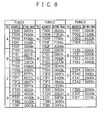
- FIG. 8 is a view showing an example of setting values to the registers from REGA to REGD in a multifunctional LSI shown in FIG. 7. It should be noted that a register from the registers REGA to REGD is supposed to be a 16-bit register.
- FIG. 9 is a view showing an example of an instruction code of the processor 71 relating to register setting stored in the instruction RAM 72.
- An instruction code 91 serves to realize the above-described first function (function 1).
- instruction codes 92, 93, and so on to realize a second function (function 2), a third function (function 3), and so on are also stored similarly.
- the total number of registers in all function blocks is about 2000 pieces, and the types of functions (search of initial base stations after power-on, a phone conversation, intermittent reception and so on) numbers several hundred. Accordingly, assuming that values are set only to several hundred registers for one function, instructions numbering 10 4 or more (the number of commands is twice the number of instructions) are to be stored. Further, a change in a cellular phone system from a PDC (Personal Digital Cellular) system to a CDMA (Code Division Multiple Access) system increases the number of types of executable functions in a multifunctional LSI and increases further the number of function blocks as well as the number of registers associated with these functions.
- PDC Personal Digital Cellular
- CDMA Code Division Multiple Access
- the capacity of the instruction RAM 72 becomes large in the multifunctional LSI, and when regions occupied by the instruction RAM 72 becomes large in the processor 71, a logical portion in the processor 71 becomes small. Further, there is a disadvantage in that the ratio of register setting processing (writing into or reading from the register) occupied in processing of the processor 71 becomes large, which disturbs effective utilization of the processing capability (processing ability such as, for instance, calculation of field intensity in a case of a cellular phone) of the processor 71 in itself.
- Patent Document 1 a method to prevent pressure of the instruction RAM 72 through stored instruction codes and to initialize plural registers is disclosed in a Patent Document 1.
- Patent Document 1
- the present invention is achieved to solve the above-described disadvantages, and the object of the present invention is to make it possible to reduce the number of instruction codes relating to register setting, so that the storage capacity of instruction RAM included in a processor can be reduced. Another object of the present invention is to allow easy coding of instruction codes for a processor which are stored in the instruction RAM.
- the present invention includes a processor having an instruction memory in which instruction to be executed is stored; a setting interface unit to which a piece of addressing information and setting values to set a plurality of registers from the processor; and an address output unit to output address values of plural registers based on the addressing information, in which the address values and the setting values are outputted from the address output unit and the setting interface unit respectively to set setting values to registers.
- the processor when setting values are set to the registers, can set the values to the registers without being aware of an address in the register by merely supplying addressing information and setting values to be set to the registers to the setting interface unit. Accordingly, addressing of each register by an instruction code stored in the instruction memory is not required, which makes it possible to reduce the number of instruction codes and coding of the instruction code can be easily performed.
- FIG. 1 is a block diagram showing a configuration example of a multifunctional semiconductor integrated circuit (multifunctional LSI) to which a semiconductor device according to an embodiment of the present invention is applied.
- multifunctional semiconductor integrated circuit multifunctional LSI
- the multifunctional LSI in the present embodiment includes a processor 1, a setting interface unit 3, an address control unit 5, and function blocks 6 to 9. It should be noted that though only four function blocks from 6 to 9 are shown to simplify explanation in FIG. 1, the number of function blocks provided by the functional LSI in the present embodiment is arbitrary.
- the setting interface unit 3 is mapped in an external memory space of the processor 1 and registers from REGA to REGD included in the function blocks 6 to 9 are mapped in a local address space which is different from the external memory space.
- the processor 1 includes an instruction RAM 2 in which instruction codes and the like for instructions to be performed by the processor 1, and performs microprocessing, register setting processing, and various control processing, and so on according to the instruction codes.
- the setting interface unit 3 function numbers showing types of functions to be realized, and setting values to realize the above functions are written by the processor 1 into a memory unit 4 provided inside via a processor bus PBUS.
- the setting interface unit 3 supplies a function number FN held in the memory unit 4 to an address control unit 5, and supplies a setting value STV to the function blocks 6 to 9. Note that the memory unit 4 will be described later.
- the address control unit 5 includes a ROM in which a table linking the function numbers and local addresses of the registers to be set is stored.
- the address control unit 5 supplies the local address LAD corresponding to the function number FN to the function block 6 to 9 based on the function number FN supplied from the setting interface unit 3. It should be noted that the processor 1 can rewrite the table at an arbitrary point of time by using a rewritable memory such as a RAM for the address control unit 5, and by connecting the rewritable memory to the processor bus PBUS and mapping it in the external memory space of the processor 1.
- a function block A6 includes a plurality of registers REGA, and is a functional unit composed of hardware realizing predetermined functions according to values set to the registers REGA.
- Function blocks B7 to D9 are composed in a similar manner to the function block A6, and realize predetermined functions according to values set in a plurality of registers from REGB to REGD which are included in the function blocks respectively.
- the function blocks 6 to 9 realize a modulation function, a demodulation function, an error-correction function, a channel coding (decoding) function and so on respectively.
- registers REGA, REGB, REGC, and REGD are mapped in regions having address values from F000 to F0FF, from F100 to F1FF, from F200 to 21FF, and from F300 to F3FF on the local address space respectively. It is also assumed that a register of the registers from REGA to REGD is a 16-bit register.
- FIG. 2 is a view showing a configuration example of the memory unit 4 which is provided in the setting interface unit 3.
- the memory unit 4 is provided to fit to the one having the maximum number of registers to set setting values among the functions to realize with the multifunctional LSI of the present embodiment.
- a memory unit 4 which is mapped in regions having address values from F000 to F016 in the external memory space in the processor 1 is shown as an example. That is, the example shows a case in which the number of registers to set a setting value is 22 pieces at the maximum to realize a certain function in a multifunctional LSI.
- a function number is written in a region having the top address of F000 in the memory unit 4, and setting values to be set to a register to realize a function are written in a region having addresses from F001 to F016.
- setting values are written in the region having the addresses from F001 to F016, only the setting values are written in succession by ascending or descending numeric order of a local address of a register where the setting values exist.
- a function number written in the region having the address of F000 is supplied to the address control unit 5, and the setting values written in the addresses from F001 to F014 are supplied to the function blocks 6 to 9.
- function numbers are to be written in a region having the address of F000, the present invention is not limited to this, an arbitrary region (address) in which a function number is written can be determined in advance, and the value written in the region can be supplied to the address control unit 5 as a function number FN.
- the setting values are to be written in succession to regions having address numbers from F001 to F016 in ascending or descending numeric order of the local address of the register, if conformity between the writing order of the setting values and the writing order of the local addresses in a table described later is maintained, the setting values can be written in succession in an arbitrary order regardless of local addresses in a register.
- FIG. 3 is a view showing an example of a table included in the address control unit 5.
- FIG. 3 shows a table of functions from 1 to 3 (FUNCs from 1 to 3), one example of which is shown in FIG. 8.
- a local address in a register for which a setting value is to be set corresponding to the function number is shown for every function number, through which a local address LAD is outputted based on the function number FN.
- F000, F008, F009, ⁇ , F380, F381 are shown as local addresses of the register to be set, and when "0001h" is supplied as the function number FN, the address control unit 5 supplies F000, F008, F009, ⁇ , F380, F381 in turn as the local addresses to the function blocks 6 to 9.
- the multifunctional LSI thus configured, when a function number and setting values to be set to registers from REGA to REGD are supplied to the setting interface unit 3 from the processor 1, the function number and setting values are written in turn into the memory unit 4 in the setting interface unit 3.
- the register setting processing associated with the processor 1 is completed with the above-described processing.
- the function number FN written in the memory unit 4 is supplied from the setting interface unit 3 to the address control unit 5, and the local addresses LAD are outputted in accordance with the function number FN from the address control unit 5.
- the local addresses outputted from the address control unit 5, and the setting values outputted from the setting interface unit 3 in accordance with the local addresses, are supplied to the function blocks 6 to 9 with a predetermined writing timing, so that setting values are set to the registers from REGA to REGD of the function blocks 6 to 9.
- an address is outputted as shown in FIG. 4.
- a setting value written in a region having an address of F001 in the setting interface unit 3 is written in a register having an address of F000 in a local address.
- setting values written in regions having addresses of F002, F003, ⁇ , F014, in the setting interface unit 3 are written in the registers having addresses of F008, F009, ⁇ , F381 in a local address respectively.
- the address control unit 5 outputs a writing pulse and the like for instance, and controls writing operation of setting values into the registers from REGA to REGD of the function blocks 6 to 9.
- FIG. 5 is a view showing an example of instruction codes and the like relating to register setting processing stored in the instruction RAM 2 in the present embodiment.
- an instruction code 51 is an instruction code to realize the above-described first function (function 1: FUNC 1).
- setting values to be set finally can be set to the registers from REGA to REGD.
- the conventional processor processes relating to an address value and a setting value alternatively in such a manner that an address value is related to a setting value which is related to another address value which is related to another setting value in turn and so on, but in the present embodiment, an addressing portion of a register for an instruction code is eliminated, and the processor only processes almost relating to setting values in such a manner that a function number to a setting value to another setting value and so on. That is, the present embodiment makes it possible to set setting values to be set to the registers REGA to REGD with nearly half the amount of processing by the processor.
- a second function (function 2: FUNC 2) and a third function (function 3: FUNC 1) by storing instruction codes 52 and 53, and data tables 55 and 56 into respective instruction RAM 2, setting values to be set can be set to the registers from REGA to REGD. Note that since data in the data tables 54, 55, 56 can be renewed based on a result of microprocessing in the processor 1, the data tables 54, 55, and 56 are provided in the instruction RAM 2.
- the processor 1 when setting values in response to functions to be realized are set into the registers from REGA to REGD, the processor 1 can set setting values to the registers from REGA to REGD by just supplying function numbers and the setting values to the setting interface unit 3 without being conscious of numerous addresses of registers from REGA to REGD to where the setting values are set.
- the register setting processing performed by the processor 1 is only to supply function numbers and setting values to be set to the registers from REGA to REGD to the setting interface unit 3, it becomes possible to reduce the processing time required for the register setting processing by the processor 1 compared with the time required conventionally. Accordingly, the original processing capacity of the processor 1 can be effectively used, or cost can be reduced by using a processor 1 having a lower processing capability (MIPS value).
- MIPS value processing capability
- FIG. 6 is a view explaining the operation of an intermittent reception processing of a cellular phone to which the multifunctional LSI in the present embodiment is applied.
- the term "intermittent reception processing” corresponds to "a processing P1" (processing 1) to monitor a paging channel (hereinafter referred to as "PCH") at predetermined time intervals (2.56 seconds shown by an intermittent reception cycle in an example shown in FIG. 6), and to confirm (call-in confirmation) whether there is a telephone call or not.
- PCH paging channel
- the intermittent control block includes a register and a timer and operates with low frequency clock signals.
- Setting values to set to registers from REGA to REGD which are necessary to receive the above PCH are defined as one of its function, and when performing an intermittent reception processing, the processor 1 supplies a function number for the PCH reception and the setting values to set to the registers from REGA to REGD to the setting interface unit 3. Then, the setting values to receive the PCH are set to the registers from REGA to REGD (processing P2), and it transits (processing 2) to receiving operation of the PCH (processing P3).
- the multifunctional LSI blocks power supply to the instruction RAM 2 in the processor 1 in a power down state, boot operation is required during the intermittent reception processing, power is supplied to the instruction RAM 2 in either of the above-described intermittent reception processing or the power down state. Accordingly, if the capacity of the instruction RAM 2 is as large as previously, a large amount of power is consumed by leakage current, which is a big disadvantage for a battery operated device, such as a cellular phone.
- the volume of the instruction RAM can be substantially reduced so that consumption of power due to leakage current in the instruction RAM 2 can also be substantially reduced.
- a function number is shown as an example to show types of functions to be realized, it is not limited to this, arbitrary information to show the types of the functions may be used. Besides, it is not limited to those showing the types of the functions, any arbitrary information to allow it to output address values of a plurality of registers can be accepted.
- one of addressing information and setting values to set to a plurality of registers are supplied from a processor having an instruction memory to a setting interface unit, and address values of a plurality of registers are outputted from an address output unit based on the addressing information, so that the outputted address values and setting values are outputted to resister respectively to set setting values.
- the processor can set setting values just by supplying addressing information and setting values to be set to the registers, without being conscious of addresses of the registers, it is possible to reduce the addressing portion by an instruction codes so that the number of the instruction codes can be reduced, which leads to reduction of storage capacity of the instruction memory included in the processor. Besides, since the instruction becomes very simple compared with the conventional ways, coding of the instruction codes can be easily performed.
Landscapes
- Engineering & Computer Science (AREA)
- Software Systems (AREA)
- Theoretical Computer Science (AREA)
- Physics & Mathematics (AREA)
- General Engineering & Computer Science (AREA)
- General Physics & Mathematics (AREA)
- Microcomputers (AREA)
- Semiconductor Integrated Circuits (AREA)
- Executing Machine-Instructions (AREA)
- Techniques For Improving Reliability Of Storages (AREA)
- Mobile Radio Communication Systems (AREA)
Abstract
Description
- The present invention relates to a semiconductor device, especially suitable to be used for a multifunctional semiconductor integrated circuit which realizes different functions according to values set in a register.
- Among semiconductor integrated circuits such as an LSI, there exists a multifunctional semiconductor integrated circuit (a multifunctional LSI) that realizes different functions according to a setting value (data) in a register. In recent years, improvements in the performance of the multifunctional LSI to get higher and more multiple functions have increased the amount of data that can be processed in the LSI. Also the number of registers to set up operation modes and various parameters to realize desired functions have increased. The setting of values to these registers is performed mainly by software or the firmware of a processor (for instance, a CPU or a DSP), which requires a considerable amount of time because of the increasing number of registers.
- FIG. 7 is a block diagram showing a configuration example of a conventional multifunctional LSI. Note that as for a functional block, only four functional blocks from 73 to 76 are shown to simplify the explanation thereof in FIG. 7.
- In FIG. 7, a
processor 71 is structured including an instruction RAM (Random Access Memory) 72, and performs various functions such as microprocessing, register setting processing, and miscellaneous control processing. Theinstruction RAM 72 serves to store instruction codes and the like for commands to be performed by theprocessor 71. - A function block A73 is a functional unit which is composed of hardware, and includes a plurality of registers REGA. The function block A73 realizes a predetermined function according to values set in the registers REGA. Function blocks B74 to D76 are composed in a similar manner to the function block A73, and realize predetermined functions according to values set in a plurality of registers REGB to REGD which are included in respective function blocks.
- The
function blocks 73 to 76 are respectively connected to a processor bus PBUS of theprocessor 71, and the registers REGA to REGD which are included in thefunction blocks 73 to 76 are mapped in an external memory space of theprocessor 71. In the following explanation, the registers REGA are assumed to be mapped in a region of address values from F000 to F0FF in the external memory space, and the registers REGB, REGC, and REGD are assumed to be mapped in the regions of address values from F100 to F1FF, from F200 to 21FF, and from F300 to F3FF in the external memory space respectively. - FIG. 8 is a view showing an example of setting values to the registers from REGA to REGD in a multifunctional LSI shown in FIG. 7. It should be noted that a register from the registers REGA to REGD is supposed to be a 16-bit register.
- For instance, in order to realize a first function (function 1: FUNC 1), "0001h" (h means it is expressed in a hexadecimal notation) is set to a register having an address of F000 of the function block A73, and "F000h" is set to a register having an address of F008, and so on. Similarly, "0001h" is set to an address of F100, "0011h" is set to an address of F101 of the function block B74, and so on, "0001h" is set to an address of F200, "FFFFh" is set to an address of F2F0 of the function block C75, and so on, and "0001h" is set to an address of F300, "4002h" is set to an address of F330 of the function block D76, and so on.
- Also, for instance, in order to realize a second function (function 2: FUNC 2) which is different from the first function, "0002h" is set to an address of F000, "F0F0h" is set to an address of F008, and so on of the function block A73, and "0002h" is set to an address of F100, "0001h" is set to an address of F101, and so on of the function block B74, and "0002h" is set to an address of F200, "000Fh" is set to an address of F2F0, and so on of the function block C75, and "0002h" is set to an address of F300, "0002h" is set to an address of F330, and so on of the function block D76.
- That is, in a multifunctional LSI as shown in FIG. 8, the number of registers to be set and their addresses differ according to the function to be realized, and even among the same registers, a setting value to be set differs according to a function. Therefore, in the
instruction RAM 72 included in theprocessor 71, an instruction code of theprocessor 71 relating to register setting is written in each function as shown in FIG. 9, and the instructions to give access to registers are redundantly and repeatedly stored. - FIG. 9 is a view showing an example of an instruction code of the
processor 71 relating to register setting stored in theinstruction RAM 72. Aninstruction code 91 serves to realize the above-described first function (function 1). An address showing a register to be set is substituted to a variable (for instance, "MOV X = F000"), and then a setting value is written into the address which is substituted into the variable (for instance, "MOV (x++0), 0001h"). That is, a value is set to a register with two commands, and this procedure is repeated for the whole registers to be set in a similar manner. Note thatinstruction codes - However, in a multifunctional LSI having many kinds of executable functions owing to increased functionality, there is a disadvantage in that the number of instruction codes stored in the
instruction RAM 72 of theprocessor 71 dramatically increases and demands greater storage capacity to theinstruction RAM 72. Another disadvantage is that the coding of instruction codes to be stored in theinstruction RAM 72 becomes very difficult. - For instance, in a multifunctional LSI used in a cellular phone, the total number of registers in all function blocks is about 2000 pieces, and the types of functions (search of initial base stations after power-on, a phone conversation, intermittent reception and so on) numbers several hundred. Accordingly, assuming that values are set only to several hundred registers for one function, instructions numbering 104 or more (the number of commands is twice the number of instructions) are to be stored. Further, a change in a cellular phone system from a PDC (Personal Digital Cellular) system to a CDMA (Code Division Multiple Access) system increases the number of types of executable functions in a multifunctional LSI and increases further the number of function blocks as well as the number of registers associated with these functions.
- As described above, the capacity of the
instruction RAM 72 becomes large in the multifunctional LSI, and when regions occupied by theinstruction RAM 72 becomes large in theprocessor 71, a logical portion in theprocessor 71 becomes small. Further, there is a disadvantage in that the ratio of register setting processing (writing into or reading from the register) occupied in processing of theprocessor 71 becomes large, which disturbs effective utilization of the processing capability (processing ability such as, for instance, calculation of field intensity in a case of a cellular phone) of theprocessor 71 in itself. - In addition, a method to prevent pressure of the
instruction RAM 72 through stored instruction codes and to initialize plural registers is disclosed in aPatent Document 1. - Japanese Patent Application Laid-open No. Hei 8-153001
- The present invention is achieved to solve the above-described disadvantages, and the object of the present invention is to make it possible to reduce the number of instruction codes relating to register setting, so that the storage capacity of instruction RAM included in a processor can be reduced. Another object of the present invention is to allow easy coding of instruction codes for a processor which are stored in the instruction RAM.
- The present invention includes a processor having an instruction memory in which instruction to be executed is stored; a setting interface unit to which a piece of addressing information and setting values to set a plurality of registers from the processor; and an address output unit to output address values of plural registers based on the addressing information, in which the address values and the setting values are outputted from the address output unit and the setting interface unit respectively to set setting values to registers.
- According to the present invention, when setting values are set to the registers, the processor can set the values to the registers without being aware of an address in the register by merely supplying addressing information and setting values to be set to the registers to the setting interface unit. Accordingly, addressing of each register by an instruction code stored in the instruction memory is not required, which makes it possible to reduce the number of instruction codes and coding of the instruction code can be easily performed.
-
- FIG. 1 is a block diagram showing a configuration example of a multifunctional semiconductor integrated circuit to which a semiconductor device according to an embodiment of the present invention is applied;
- FIG. 2 is a view showing a configuration example of a memory unit provided to a setting interface unit.
- FIG. 3 is a view showing an example of a table included in the address control unit;
- FIG. 4 is a view to explain a conversion example of a function number vs. a local address in the present embodiment;
- FIG. 5 is a view showing a configuration of an instruction RAM in the present embodiment;
- FIG. 6 is a view to explain the operation of an intermittent reception processing of a cellular phone to which the present embodiment is applied;
- FIG. 7 is a block diagram showing a configuration example of a conventional multifunctional LSI;
- FIG. 8 is a view showing an example of setting values to set to registers; and
- FIG. 9 is a view showing a configuration example of instruction codes relating to register setting written in the instruction RAM shown in FIG. 7.
-
- Hereinafter, an embodiment of the present invention will be explained based on the drawing.
- FIG. 1 is a block diagram showing a configuration example of a multifunctional semiconductor integrated circuit (multifunctional LSI) to which a semiconductor device according to an embodiment of the present invention is applied.
- The multifunctional LSI in the present embodiment includes a
processor 1, a setting interface unit 3, an address control unit 5, and function blocks 6 to 9. It should be noted that though only four function blocks from 6 to 9 are shown to simplify explanation in FIG. 1, the number of function blocks provided by the functional LSI in the present embodiment is arbitrary. - In the multifunctional LSI in the present embodiment, the setting interface unit 3 is mapped in an external memory space of the
processor 1 and registers from REGA to REGD included in thefunction blocks 6 to 9 are mapped in a local address space which is different from the external memory space. - The
processor 1 includes aninstruction RAM 2 in which instruction codes and the like for instructions to be performed by theprocessor 1, and performs microprocessing, register setting processing, and various control processing, and so on according to the instruction codes. - In the setting interface unit 3, function numbers showing types of functions to be realized, and setting values to realize the above functions are written by the
processor 1 into amemory unit 4 provided inside via a processor bus PBUS. The setting interface unit 3 supplies a function number FN held in thememory unit 4 to an address control unit 5, and supplies a setting value STV to the function blocks 6 to 9. Note that thememory unit 4 will be described later. - The address control unit 5 includes a ROM in which a table linking the function numbers and local addresses of the registers to be set is stored. The address control unit 5 supplies the local address LAD corresponding to the function number FN to the
function block 6 to 9 based on the function number FN supplied from the setting interface unit 3. It should be noted that theprocessor 1 can rewrite the table at an arbitrary point of time by using a rewritable memory such as a RAM for the address control unit 5, and by connecting the rewritable memory to the processor bus PBUS and mapping it in the external memory space of theprocessor 1. - A function block A6 includes a plurality of registers REGA, and is a functional unit composed of hardware realizing predetermined functions according to values set to the registers REGA. Function blocks B7 to D9 are composed in a similar manner to the function block A6, and realize predetermined functions according to values set in a plurality of registers from REGB to REGD which are included in the function blocks respectively. For instance, when the multifunctional LSI in the present embodiment is used in a cellular phone, the function blocks 6 to 9 realize a modulation function, a demodulation function, an error-correction function, a channel coding (decoding) function and so on respectively.
- It should be noted that in the following explanation, it is assumed that registers REGA, REGB, REGC, and REGD are mapped in regions having address values from F000 to F0FF, from F100 to F1FF, from F200 to 21FF, and from F300 to F3FF on the local address space respectively. It is also assumed that a register of the registers from REGA to REGD is a 16-bit register.
- FIG. 2 is a view showing a configuration example of the
memory unit 4 which is provided in the setting interface unit 3. Thememory unit 4 is provided to fit to the one having the maximum number of registers to set setting values among the functions to realize with the multifunctional LSI of the present embodiment. In FIG. 2, amemory unit 4 which is mapped in regions having address values from F000 to F016 in the external memory space in theprocessor 1 is shown as an example. That is, the example shows a case in which the number of registers to set a setting value is 22 pieces at the maximum to realize a certain function in a multifunctional LSI. - As shown in FIG. 2, a function number is written in a region having the top address of F000 in the
memory unit 4, and setting values to be set to a register to realize a function are written in a region having addresses from F001 to F016. When setting values are written in the region having the addresses from F001 to F016, only the setting values are written in succession by ascending or descending numeric order of a local address of a register where the setting values exist. As described above, a function number written in the region having the address of F000 is supplied to the address control unit 5, and the setting values written in the addresses from F001 to F014 are supplied to the function blocks 6 to 9. - For instance, as shown in FIG. 2, when setting values of the first function (function 1: FUNC 1) shown in FIG. 8 are written, "0001h" is written in a region having an address of F000, and "0001h", "F000h", ···, "0100h", "0001h" are written in the following addresses from F001 to F014 in order. Writing is not performed in regions having addresses of F015 and F016 where no setting value to be written exists (or arbitrary values are written and thus written values are neglected in following operations).
- In the explanation described above, though function numbers are to be written in a region having the address of F000, the present invention is not limited to this, an arbitrary region (address) in which a function number is written can be determined in advance, and the value written in the region can be supplied to the address control unit 5 as a function number FN.
- Further, though the setting values are to be written in succession to regions having address numbers from F001 to F016 in ascending or descending numeric order of the local address of the register, if conformity between the writing order of the setting values and the writing order of the local addresses in a table described later is maintained, the setting values can be written in succession in an arbitrary order regardless of local addresses in a register.
- FIG. 3 is a view showing an example of a table included in the address control unit 5. FIG. 3 shows a table of functions from 1 to 3 (FUNCs from 1 to 3), one example of which is shown in FIG. 8.
- As shown in FIG. 3, a local address in a register for which a setting value is to be set corresponding to the function number, is shown for every function number, through which a local address LAD is outputted based on the function number FN. For instance, as for function 1 (FUNC 1), F000, F008, F009, ···, F380, F381 are shown as local addresses of the register to be set, and when "0001h" is supplied as the function number FN, the address control unit 5 supplies F000, F008, F009, ···, F380, F381 in turn as the local addresses to the function blocks 6 to 9.
- In the multifunctional LSI thus configured, when a function number and setting values to be set to registers from REGA to REGD are supplied to the setting interface unit 3 from the
processor 1, the function number and setting values are written in turn into thememory unit 4 in the setting interface unit 3. The register setting processing associated with theprocessor 1 is completed with the above-described processing. Then, the function number FN written in thememory unit 4 is supplied from the setting interface unit 3 to the address control unit 5, and the local addresses LAD are outputted in accordance with the function number FN from the address control unit 5. - Thus, the local addresses outputted from the address control unit 5, and the setting values outputted from the setting interface unit 3 in accordance with the local addresses, are supplied to the function blocks 6 to 9 with a predetermined writing timing, so that setting values are set to the registers from REGA to REGD of the function blocks 6 to 9.
- For instance, in a case of the function 1 (the function number FN is "0001h"), an address is outputted as shown in FIG. 4. A setting value written in a region having an address of F001 in the setting interface unit 3 is written in a register having an address of F000 in a local address. Similarly, setting values written in regions having addresses of F002, F003,···, F014, in the setting interface unit 3 are written in the registers having addresses of F008, F009, ···, F381 in a local address respectively.
- At this time, the address control unit 5 outputs a writing pulse and the like for instance, and controls writing operation of setting values into the registers from REGA to REGD of the function blocks 6 to 9.
- By taking the above-described configuration, coding of an instruction code of the
processor 1 shown in FIG. 5 becomes possible in the present embodiment. FIG. 5 is a view showing an example of instruction codes and the like relating to register setting processing stored in theinstruction RAM 2 in the present embodiment. In FIG. 5, aninstruction code 51 is an instruction code to realize the above-described first function (function 1: FUNC 1). - First, a leading address (F000) of the
memory unit 4 in the setting interface unit 3 is substituted into a variable X (MOV X=A), then data in a data table (TBL_DTA) 54 in theinstruction RAM 2 in which only setting values are arranged is obtained and is substituted into a variable Y (MOV Y=TBL_DTA). Then, the value substituted into the variable Y is written into the address substituted into variable X in the setting interface unit 3. That is, a setting value is written into the setting interface unit 3 (MOV (X++) , (Y++) h) . - By successively incrementing the variable X (address) through a LOOP form or the like, setting values to be set finally can be set to the registers from REGA to REGD. Accordingly, the conventional processor processes relating to an address value and a setting value alternatively in such a manner that an address value is related to a setting value which is related to another address value which is related to another setting value in turn and so on, but in the present embodiment, an addressing portion of a register for an instruction code is eliminated, and the processor only processes almost relating to setting values in such a manner that a function number to a setting value to another setting value and so on. That is, the present embodiment makes it possible to set setting values to be set to the registers REGA to REGD with nearly half the amount of processing by the processor.
- It should be noted that as for a second function (function 2: FUNC 2) and a third function (function 3: FUNC 1) by storing instruction codes 52 and 53, and data tables 55 and 56 into
respective instruction RAM 2, setting values to be set can be set to the registers from REGA to REGD. Note that since data in the data tables 54, 55, 56 can be renewed based on a result of microprocessing in theprocessor 1, the data tables 54, 55, and 56 are provided in theinstruction RAM 2. - As explained in detail above, according to the present embodiment, when setting values in response to functions to be realized are set into the registers from REGA to REGD, the
processor 1 can set setting values to the registers from REGA to REGD by just supplying function numbers and the setting values to the setting interface unit 3 without being conscious of numerous addresses of registers from REGA to REGD to where the setting values are set. - Accordingly, the necessity to include addressing portion in an instruction code relating to register setting to store in the
instruction RAM 2 disappears, and as is understood by comparing an instruction code according to the present embodiment shown in FIG. 5 and a conventional instruction code shown in FIG. 9, it becomes possible to reduce the number of instruction codes so as to reduce storage capacity to be provided by theinstruction RAM 2, which facilitates coding of the instruction code. Besides, when a portion of a setting value is modified, since address values and setting values are mixedly existed previously, it may cause a mistake in the modification. However, in the present embodiment, since only setting values are shown, it becomes possible to reduce the probability of mistake in modification. - The register setting processing performed by the
processor 1 is only to supply function numbers and setting values to be set to the registers from REGA to REGD to the setting interface unit 3, it becomes possible to reduce the processing time required for the register setting processing by theprocessor 1 compared with the time required conventionally. Accordingly, the original processing capacity of theprocessor 1 can be effectively used, or cost can be reduced by using aprocessor 1 having a lower processing capability (MIPS value). - A concrete example of applying a multifunctional LSI according to the present embodiment described above to a cellular phone, will be explained below.
- FIG. 6 is a view explaining the operation of an intermittent reception processing of a cellular phone to which the multifunctional LSI in the present embodiment is applied. The term "intermittent reception processing" corresponds to "a processing P1" (processing 1) to monitor a paging channel (hereinafter referred to as "PCH") at predetermined time intervals (2.56 seconds shown by an intermittent reception cycle in an example shown in FIG. 6), and to confirm (call-in confirmation) whether there is a telephone call or not.
- As a result of the confirmation, if there is no telephone call, it transits to a power down state (operating state in low power consumption) in which only intermittent control block is allowed to operate and power supply of other function blocks is suspended, and in the case of having a telephone call, steps to start a phone conversation are carried out. The intermittent control block includes a register and a timer and operates with low frequency clock signals.
- Setting values to set to registers from REGA to REGD which are necessary to receive the above PCH are defined as one of its function, and when performing an intermittent reception processing, the
processor 1 supplies a function number for the PCH reception and the setting values to set to the registers from REGA to REGD to the setting interface unit 3. Then, the setting values to receive the PCH are set to the registers from REGA to REGD (processing P2), and it transits (processing 2) to receiving operation of the PCH (processing P3). - Since the multifunctional LSI blocks power supply to the
instruction RAM 2 in theprocessor 1 in a power down state, boot operation is required during the intermittent reception processing, power is supplied to theinstruction RAM 2 in either of the above-described intermittent reception processing or the power down state. Accordingly, if the capacity of theinstruction RAM 2 is as large as previously, a large amount of power is consumed by leakage current, which is a big disadvantage for a battery operated device, such as a cellular phone. However, according to the present embodiment, since the storage capacity required of theinstruction RAM 2 can be largely reduced as described above, the volume of the instruction RAM can be substantially reduced so that consumption of power due to leakage current in theinstruction RAM 2 can also be substantially reduced. - Note that as for other examples of functions when the multifunctional LSI according to the present embodiment is applied to a cellular phone, initial base station search, a telephone call and so on after power on can be cited.
- It should be noted that in the above-described embodiment, though a function number is shown as an example to show types of functions to be realized, it is not limited to this, arbitrary information to show the types of the functions may be used. Besides, it is not limited to those showing the types of the functions, any arbitrary information to allow it to output address values of a plurality of registers can be accepted.
- The present embodiments are to be considered in all respects as illustrative and no restrictive, and all changes which come within the meaning and range of equivalency of the claims are therefore intended to be embraced therein. The invention may be embodied in other specific forms without departing from the spirit or essential characteristics thereof.
- As described above, according to the present invention, one of addressing information and setting values to set to a plurality of registers are supplied from a processor having an instruction memory to a setting interface unit, and address values of a plurality of registers are outputted from an address output unit based on the addressing information, so that the outputted address values and setting values are outputted to resister respectively to set setting values.
- Through this procedure, since the processor can set setting values just by supplying addressing information and setting values to be set to the registers, without being conscious of addresses of the registers, it is possible to reduce the addressing portion by an instruction codes so that the number of the instruction codes can be reduced, which leads to reduction of storage capacity of the instruction memory included in the processor. Besides, since the instruction becomes very simple compared with the conventional ways, coding of the instruction codes can be easily performed.
Claims (16)
- A semiconductor device comprising:wherein said setting values outputted from said setting interface unit are set to said registers, using said address values outputted from said address output unit.a processor having an instruction memory in which an instruction to be executed is stored and connected to a first bus;a setting interface unit connected to said first bus, and supplied with one piece of addressing information and setting values to be set to a plurality of registers from said processor; andan address output unit outputting address values of said plural registers based on said addressing information supplied from said setting interface unit;
- The semiconductor device according to claim 1, wherein said address output unit includes a table linking said addressing information with address values of said plural registers in accordance with the addressing information.
- The semiconductor device according to claim 2, wherein said table is stored in a read only memory.
- The semiconductor device according to claim 2, wherein said table is stored in a rewritable memory connected to said first bus.
- The semiconductor device according to claim 1, wherein said setting interface unit includes a memory unit to store said addressing information and setting values to be set to said registers.
- The semiconductor device according to claim 5, wherein said memory unit has storage capacity in accordance with the maximum number of setting values to be set to registers which can be supplied from said processor.
- The semiconductor device according to claim 5, wherein setting values to be set to said plural registers supplied from said processor are written in continuous regions of said memory unit.
- A semiconductor device including a function unit capable of realizing different functions according to setting values to be set to registers, said semiconductor device comprising:wherein said setting values to be outputted by said setting interface unit are set to said registers using said address values outputted by said address output unit.a processor having an instruction memory in which an instruction to be executed is stored, and connected to a first bus;a setting interface unit, connected to said first bus, and supplied with one piece of function information showing a realizable function and setting values to be set to a plurality of registers to realize the function, from said processor; andan address output unit outputting address values of said plural registers based on said function information supplied from said setting interface unit,
- The semiconductor device according to claim 8, wherein said address output unit includes a table linking said function information with address values of said plural registers in accordance with the function information.
- The semiconductor device according to claim 8, wherein said setting interface unit includes a memory unit to store said function information and setting values to be set to said registers,
wherein said memory unit has storage capacity in accordance with the maximum number of setting values to be set to registers which can be supplied from said processor. - The semiconductor device according to claim 8, further comprising:wherein the power supply to other functional units different from the intermittent control function unit is suspended according to the execution result of said intermittent processing.a plurality of said functional units including an intermittent control functional unit to allow other functional units to execute an intermittent processing at fixed intervals,
- The semiconductor device according to claim 11, wherein the intermittent processing comprises an intermittent reception processing to perform call-in confirmation.
- A semiconductor device comprising:wherein said setting values outputted from said setting interface unit are set to said registers using said local address values outputted from said address output unit.a processor having an instruction memory in which instructions to be executed are stored;a plurality of registers disposed in a local address space different from an address space of said processor;a setting interface unit disposed in the address space of said processor, and supplied with one piece of addressing information and setting values to be set to said plural registers from said processor; andan address output unit outputting local address values of said plural registers based on said addressing information supplied from said setting interface unit,
- The semiconductor device according to claim 13, wherein said address output unit includes a table linking said addressing information with local address values of said plural registers.
- The semiconductor device according to claim 13, wherein said setting interface unit includes a memory unit to store said addressing information and setting values to be set to said registers,
wherein said memory unit has storage capacity in accordance with the maximum number of setting values to be set to registers which can be supplied from said processor. - The semiconductor device according to claim 13, wherein said register is a register provided in a functional unit to realize different functions according to setting values.
Applications Claiming Priority (1)
| Application Number | Priority Date | Filing Date | Title |
|---|---|---|---|
| PCT/JP2003/004055 WO2004088528A1 (en) | 2003-03-31 | 2003-03-31 | Semiconductor device |
Publications (2)
| Publication Number | Publication Date |
|---|---|
| EP1610226A1 true EP1610226A1 (en) | 2005-12-28 |
| EP1610226A4 EP1610226A4 (en) | 2009-05-06 |
Family
ID=33105332
Family Applications (1)
| Application Number | Title | Priority Date | Filing Date |
|---|---|---|---|
| EP03715634A Withdrawn EP1610226A4 (en) | 2003-03-31 | 2003-03-31 | Semiconductor device |
Country Status (7)
| Country | Link |
|---|---|
| US (1) | US7260710B2 (en) |
| EP (1) | EP1610226A4 (en) |
| JP (1) | JP4241625B2 (en) |
| CN (1) | CN100474284C (en) |
| AU (1) | AU2003220994A1 (en) |
| TW (1) | TWI240888B (en) |
| WO (1) | WO2004088528A1 (en) |
Families Citing this family (3)
| Publication number | Priority date | Publication date | Assignee | Title |
|---|---|---|---|---|
| KR100615694B1 (en) * | 2004-08-16 | 2006-08-25 | 삼성전자주식회사 | Control system for controlling plural function block |
| JP2010122787A (en) * | 2008-11-18 | 2010-06-03 | Panasonic Corp | Semiconductor integrated circuit and register address control device |
| GB2493340A (en) * | 2011-07-28 | 2013-02-06 | St Microelectronics Res & Dev | Address mapping of boot transactions between dies in a system in package |
Citations (3)
| Publication number | Priority date | Publication date | Assignee | Title |
|---|---|---|---|---|
| JP2001022685A (en) * | 1999-07-13 | 2001-01-26 | Mitsubishi Electric Corp | Device and method for transferring data |
| JP2001068993A (en) * | 1999-08-25 | 2001-03-16 | Fuji Xerox Co Ltd | Information processing system |
| US20020174266A1 (en) * | 2001-05-18 | 2002-11-21 | Krishna Palem | Parameterized application programming interface for reconfigurable computing systems |
Family Cites Families (4)
| Publication number | Priority date | Publication date | Assignee | Title |
|---|---|---|---|---|
| JPH025115A (en) * | 1988-06-24 | 1990-01-10 | Hitachi Ltd | Initializing system for register |
| JPH096483A (en) * | 1995-06-20 | 1997-01-10 | Hitachi Ltd | Microcomputer and portable telephone set |
| US6820191B2 (en) * | 2000-12-05 | 2004-11-16 | Faraday Technology Corp. | Apparatus and method for executing an instruction with a register bit mask for transferring data between a plurality of registers and memory inside a processor |
| KR100447178B1 (en) * | 2001-12-18 | 2004-09-04 | 엘지전자 주식회사 | Finite impulse response filter |
-
2003
- 2003-03-31 TW TW092107294A patent/TWI240888B/en not_active IP Right Cessation
- 2003-03-31 WO PCT/JP2003/004055 patent/WO2004088528A1/en active Application Filing
- 2003-03-31 AU AU2003220994A patent/AU2003220994A1/en not_active Abandoned
- 2003-03-31 JP JP2004570150A patent/JP4241625B2/en not_active Expired - Fee Related
- 2003-03-31 CN CNB038257602A patent/CN100474284C/en not_active Expired - Fee Related
- 2003-03-31 EP EP03715634A patent/EP1610226A4/en not_active Withdrawn
-
2005
- 2005-03-29 US US11/091,584 patent/US7260710B2/en active Active
Patent Citations (3)
| Publication number | Priority date | Publication date | Assignee | Title |
|---|---|---|---|---|
| JP2001022685A (en) * | 1999-07-13 | 2001-01-26 | Mitsubishi Electric Corp | Device and method for transferring data |
| JP2001068993A (en) * | 1999-08-25 | 2001-03-16 | Fuji Xerox Co Ltd | Information processing system |
| US20020174266A1 (en) * | 2001-05-18 | 2002-11-21 | Krishna Palem | Parameterized application programming interface for reconfigurable computing systems |
Non-Patent Citations (1)
| Title |
|---|
| See also references of WO2004088528A1 * |
Also Published As
| Publication number | Publication date |
|---|---|
| JPWO2004088528A1 (en) | 2006-07-06 |
| JP4241625B2 (en) | 2009-03-18 |
| CN1720515A (en) | 2006-01-11 |
| US7260710B2 (en) | 2007-08-21 |
| TW200419441A (en) | 2004-10-01 |
| TWI240888B (en) | 2005-10-01 |
| AU2003220994A1 (en) | 2004-10-25 |
| WO2004088528A1 (en) | 2004-10-14 |
| CN100474284C (en) | 2009-04-01 |
| US20050210230A1 (en) | 2005-09-22 |
| EP1610226A4 (en) | 2009-05-06 |
Similar Documents
| Publication | Publication Date | Title |
|---|---|---|
| TWI403954B (en) | Electronic system, microcontrollers with instruction sets and method for executing instruction thererof | |
| JPH08505965A (en) | Context switching device and method | |
| US20050198471A1 (en) | Micro-controller for reading out compressed instruction code and program memory for compressing instruction code and storing therein | |
| KR101132484B1 (en) | System and method of executing instructions in a multi-stage data processing pipeline | |
| US6415338B1 (en) | System for writing a data value at a starting address to a number of consecutive locations equal to a segment length identifier | |
| EP2734918B1 (en) | Table call instruction for frequently called functions | |
| US7260710B2 (en) | Initializing function block registers using value supplying setting interface coupled to table linking block identifier to multiple register address set | |
| JP5186802B2 (en) | Microprocessor | |
| JP3578735B2 (en) | Information processing apparatus and information processing method | |
| KR100773800B1 (en) | Semiconductor device | |
| JP3562215B2 (en) | Microcomputer and electronic equipment | |
| US7093148B2 (en) | Microcontroller Operable in normal and low speed modes utilizing control signals for executing commands in a read-only memory during the low speed modes | |
| JP2826309B2 (en) | Information processing device | |
| US7290153B2 (en) | System, method, and apparatus for reducing power consumption in a microprocessor | |
| US6760834B2 (en) | Microprocessor for saving contextual data when switching to a test program | |
| JPH01205339A (en) | Microcomputer system | |
| JP2005242621A (en) | Semiconductor device and its interrupt processing method | |
| JPH07129398A (en) | Microprocessor | |
| WO1998044408A1 (en) | Microcomputer and electronic equipment | |
| JP3586689B2 (en) | Arithmetic device and arithmetic device design method | |
| JPH11316691A (en) | Execution method for operating system and information processor using the method | |
| JP2000259489A (en) | Data storage device | |
| JPH073030U (en) | Microprocessor control unit | |
| JPH10260829A (en) | Micro computer | |
| JPH073659B2 (en) | Microprocessor |
Legal Events
| Date | Code | Title | Description |
|---|---|---|---|
| PUAI | Public reference made under article 153(3) epc to a published international application that has entered the european phase |
Free format text: ORIGINAL CODE: 0009012 |
|
| 17P | Request for examination filed |
Effective date: 20051024 |
|
| AK | Designated contracting states |
Kind code of ref document: A1 Designated state(s): AT BE BG CH CY CZ DE DK EE ES FI FR GB GR HU IE IT LI LU MC NL PT RO SE SI SK TR |
|
| AX | Request for extension of the european patent |
Extension state: AL LT LV MK |
|
| DAX | Request for extension of the european patent (deleted) | ||
| RBV | Designated contracting states (corrected) |
Designated state(s): DE FR GB IT |
|
| RAP1 | Party data changed (applicant data changed or rights of an application transferred) |
Owner name: FUJITSU MICROELECTRONICS LIMITED |
|
| A4 | Supplementary search report drawn up and despatched |
Effective date: 20090406 |
|
| RAP1 | Party data changed (applicant data changed or rights of an application transferred) |
Owner name: FUJITSU SEMICONDUCTOR LIMITED |
|
| RAP1 | Party data changed (applicant data changed or rights of an application transferred) |
Owner name: SOCIONEXT INC. |
|
| 17Q | First examination report despatched |
Effective date: 20160414 |
|
| STAA | Information on the status of an ep patent application or granted ep patent |
Free format text: STATUS: THE APPLICATION IS DEEMED TO BE WITHDRAWN |
|
| 18D | Application deemed to be withdrawn |
Effective date: 20160825 |