EP1608040A1 - Anisotropic conductive connector, conductive paste composition, probe member, wafer inspection device and wafer inspection method - Google Patents
Anisotropic conductive connector, conductive paste composition, probe member, wafer inspection device and wafer inspection method Download PDFInfo
- Publication number
- EP1608040A1 EP1608040A1 EP04722670A EP04722670A EP1608040A1 EP 1608040 A1 EP1608040 A1 EP 1608040A1 EP 04722670 A EP04722670 A EP 04722670A EP 04722670 A EP04722670 A EP 04722670A EP 1608040 A1 EP1608040 A1 EP 1608040A1
- Authority
- EP
- European Patent Office
- Prior art keywords
- conductive
- anisotropically conductive
- wafer
- inspection
- particles
- Prior art date
- Legal status (The legal status is an assumption and is not a legal conclusion. Google has not performed a legal analysis and makes no representation as to the accuracy of the status listed.)
- Withdrawn
Links
Images







Classifications
-
- H—ELECTRICITY
- H01—ELECTRIC ELEMENTS
- H01R—ELECTRICALLY-CONDUCTIVE CONNECTIONS; STRUCTURAL ASSOCIATIONS OF A PLURALITY OF MUTUALLY-INSULATED ELECTRICAL CONNECTING ELEMENTS; COUPLING DEVICES; CURRENT COLLECTORS
- H01R11/00—Individual connecting elements providing two or more spaced connecting locations for conductive members which are, or may be, thereby interconnected, e.g. end pieces for wires or cables supported by the wire or cable and having means for facilitating electrical connection to some other wire, terminal, or conductive member, blocks of binding posts
- H01R11/01—Individual connecting elements providing two or more spaced connecting locations for conductive members which are, or may be, thereby interconnected, e.g. end pieces for wires or cables supported by the wire or cable and having means for facilitating electrical connection to some other wire, terminal, or conductive member, blocks of binding posts characterised by the form or arrangement of the conductive interconnection between the connecting locations
-
- G—PHYSICS
- G01—MEASURING; TESTING
- G01R—MEASURING ELECTRIC VARIABLES; MEASURING MAGNETIC VARIABLES
- G01R1/00—Details of instruments or arrangements of the types included in groups G01R5/00 - G01R13/00 and G01R31/00
- G01R1/02—General constructional details
- G01R1/06—Measuring leads; Measuring probes
- G01R1/067—Measuring probes
- G01R1/073—Multiple probes
- G01R1/07307—Multiple probes with individual probe elements, e.g. needles, cantilever beams or bump contacts, fixed in relation to each other, e.g. bed of nails fixture or probe card
- G01R1/0735—Multiple probes with individual probe elements, e.g. needles, cantilever beams or bump contacts, fixed in relation to each other, e.g. bed of nails fixture or probe card arranged on a flexible frame or film
-
- H—ELECTRICITY
- H01—ELECTRIC ELEMENTS
- H01R—ELECTRICALLY-CONDUCTIVE CONNECTIONS; STRUCTURAL ASSOCIATIONS OF A PLURALITY OF MUTUALLY-INSULATED ELECTRICAL CONNECTING ELEMENTS; COUPLING DEVICES; CURRENT COLLECTORS
- H01R13/00—Details of coupling devices of the kinds covered by groups H01R12/70 or H01R24/00 - H01R33/00
- H01R13/02—Contact members
- H01R13/22—Contacts for co-operating by abutting
- H01R13/24—Contacts for co-operating by abutting resilient; resiliently-mounted
- H01R13/2407—Contacts for co-operating by abutting resilient; resiliently-mounted characterized by the resilient means
- H01R13/2414—Contacts for co-operating by abutting resilient; resiliently-mounted characterized by the resilient means conductive elastomers
-
- H—ELECTRICITY
- H10—SEMICONDUCTOR DEVICES; ELECTRIC SOLID-STATE DEVICES NOT OTHERWISE PROVIDED FOR
- H10P—GENERIC PROCESSES OR APPARATUS FOR THE MANUFACTURE OR TREATMENT OF DEVICES COVERED BY CLASS H10
- H10P74/00—Testing or measuring during manufacture or treatment of wafers, substrates or devices
-
- H—ELECTRICITY
- H10—SEMICONDUCTOR DEVICES; ELECTRIC SOLID-STATE DEVICES NOT OTHERWISE PROVIDED FOR
- H10W—GENERIC PACKAGES, INTERCONNECTIONS, CONNECTORS OR OTHER CONSTRUCTIONAL DETAILS OF DEVICES COVERED BY CLASS H10
- H10W70/00—Package substrates; Interposers; Redistribution layers [RDL]
- H10W70/60—Insulating or insulated package substrates; Interposers; Redistribution layers
- H10W70/62—Insulating or insulated package substrates; Interposers; Redistribution layers characterised by their interconnections
- H10W70/63—Vias, e.g. via plugs
- H10W70/635—Through-vias
Definitions
- the present invention relates to an anisotropically conductive connector suitable for use in conducting electrical inspection of printed circuit boards, integrated circuit devices, integrated circuits formed on a wafer, liquid crystal panels, in which circuits have been formed, etc., a conductive paste composition for obtaining this anisotropically conductive connector, a probe member equipped with this anisotropically conductive connector, a wafer inspection apparatus equipped with this probe member, and a wafer inspection method using this probe member, and particularly to an anisotropically conductive connector suitable for use in conducting electrical inspection, such as a probe test or a burn-in test, as to integrated circuits formed on a wafer, a conductive paste composition for obtaining this anisotropically conductive connector, a probe member equipped with this anisotropically conductive connector, a wafer inspection apparatus equipped with this probe member, and a wafer inspection method using this probe member.
- a probe test for sorting defective integrated circuits is generally conducted as to each of these integrated circuit, by inspecting basic electrical properties.
- This probe test is conducted under a temperature environment of, for example, 85°C.
- This wafer is then cut, thereby forming semiconductor chips.
- semiconductor chips are contained and sealed in respective proper packages.
- Each of the packaged semiconductor integrated circuit devices is further subjected to a burn-in test that electrical properties thereof are inspected under a high-temperature environment of, for example, 125°C, thereby sorting semiconductor integrated circuit devices having latent defects.
- a probe member is in use for electrically connecting each of electrodes to be inspected in an object of inspection to a tester.
- a probe member is known a member composed of a circuit board for inspection, on which inspection electrodes have been formed in accordance with a pattern corresponding to a pattern of electrodes to be inspected, and an anisotropically conductive elastomer sheet arranged on this circuit board for inspection.
- anisotropically conductive elastomer sheets those of various structures have heretofore been known.
- Prior Art. 1 or the like discloses an anisotropically conductive elastomer sheet (hereinafter referred to as "dispersion type anisotropically conductive elastomer sheet") obtained by dispersing conductive particles in an elastomer in a state oriented so as to align in a thickness-wise direction of the elastomer, and the following Prior Art.
- an anisotropically conductive elastomer sheet (hereinafter referred to as "uneven distribution type anisotropically conductive elastomer sheet") obtained by unevenly distributing conductive particles in an elastomer in a state oriented so as to align in a thickness-wise direction of the elastomer, thereby forming a great number of conductive parts extending in the thickness-wise direction and an insulating part for mutually insulating them.
- Prior Art. 3 or the like discloses an uneven distribution type anisotropically conductive elastomer sheet with a difference in level defined between the surface of the conductive part and an insulating part.
- the conductive parts are formed in accordance with a pattern corresponding to a pattern of electrodes to be inspected of an integrated circuit to be inspected, it is advantageous compared with the dispersion type anisotropically conductive elastomer sheet in that electrical connection between electrodes can be achieved with high reliability even to an integrated circuit small in the arrangement pitch of electrodes to be inspected, i.e., center distance between adjacent electrodes to be inspected.
- an anisotropically conductive elastomer sheet used in a probe member for conducting the probe test is required to have durability capable of withstanding repeated use of, for example, at least 50,000 times when wafers that are an object of inspection are mass-produced products.
- an anisotropically conductive elastomer sheet used in a probe member for conducting the WLBI test is required to have durability capable of withstanding repeated use of, for example, at least 500 times when wafers that are an object of inspection are mass-produced products.
- a flip chip mounting method semiconductor chips, in which a semi-spherical projected electrode composed of eutectic solder, lead-free solder, high-temperature solder (lead-rich solder) or the like has been formed on surface electrodes, are used. In order to obtain such semiconductor chips at high efficiency, it is conducted to form a projected electrode on electrodes in respective integrated circuits in a state of a wafer.
- an anisotropically conductive elastomer sheet used in the probe test of a wafer is also required to have durability capable of withstanding repeated use over a great number of times even when the wafer, which is an object of inspection, has projected electrodes to be inspected.
- the present invention has been made on the basis of the foregoing circumstances and has as its first object the provision of an anisotropically conductive connector, by which good conductivity is retained over a long period of time even when it is used in electrical inspection of a plurality of integrated circuits formed on a wafer repeatedly over a great number of times, and thus high durability and long service life are achieved.
- a second object of the present invention is to provide an anisotropically conductive connector, by which good conductivity is retained over a long period of time even when it is used in electrical inspection of a plurality of integrated circuits formed on a wafer repeatedly over a great number of times, and electrodes to be inspected of the integrated circuits formed on the wafer are projected electrodes, and thus high durability and long service life are achieved.
- a third object of the present invention is to provide an anisotropically conductive connector, by which good conductivity is retained over a long period of time even when it is used in electrical inspection of a plurality of integrated circuits formed on a wafer repeatedly over a great number of times, and the electrical inspection is conducted under a high-temperature environment, and thus high durability and long service life are achieved.
- a fourth object of the present invention is to provide an anisotropically conductive connector, by which good conductivity is retained over a long period of time even when it is used in direct contact with electrodes to be inspected of integrated circuits formed on a wafer repeatedly over a great number of times, and thus high durability and long service life are achieved, in addition to the above objects.
- a fifth object of the present invention is to provide an anisotropically conductive connector, by which good conductivity is retained over a long period of time even when it is used in electrical inspection of circuit parts repeatedly over a great number of times, and the electrical inspection is conducted under a high-temperature environment, and thus high durability and long service life are achieved.
- a sixth object of the present invention is to provide a conductive paste composition suitable for use in forming elastic anisotropically conductive films in the above-described anisotropically conductive connectors.
- a seventh object of the present invention is to provide a probe member, by which good conductivity is retained over a long period of time even when it is used in electrical inspection of a plurality of integrated circuits formed on a wafer repeatedly over a great number of times, and thus high durability and long service life are achieved.
- An eighth object of the present invention is to provide a wafer inspection apparatus and a wafer inspection method for conducting electrical inspection of a plurality of integrated circuits formed on a wafer in a state of the wafer using the above-described probe member.
- the present inventors have carried out an extensive investigations repeatedly as to the cause of marked deterioration of the conductivity of conductive parts when an anisotropically conductive connector is used repeatedly.
- gold forming a coating layer in conductive particles is low in hardness as a metal, separation, abrasion, deformation and/or the like occurs on the coating layer in the conductive particles by contact between the conductive particles and contact between the conductive particles and an electrode to be inspected as the anisotropically conductive connector is used repeatedly, and consequently core particles composed of nickel or the like are exposed to the surface, thereby markedly deteriorating the conductivity of the conductive parts, and the present invention has been completed on the basis of this finding.
- an anisotropically conductive connector comprising an elastic anisotropically conductive film, in which a plurality of conductive parts for connection containing conductive particles and extending in a thickness-wise direction of the film have been formed, wherein the conductive particles contained in the conductive parts for connection are obtained by laminating a coating layer formed of a high-conductive metal on a surface of core particle exhibiting magnetism, and the coating layer is a coating layer having a high hardness.
- an anisotropically conductive connector comprising an elastic anisotropically conductive film, in which a plurality of conductive parts for connection containing conductive particles and extending in a thickness-wise direction of the film have been formed, wherein the conductive particles contained in the conductive parts for connection are obtained by laminating a plurality of coating layers each formed of a high-conductive metal on a surface of core particle exhibiting magnetism, and the outermost coating layer among the plurality of the coating layers is a coating layer having a high hardness.
- the Vickers hardness (HV) of the coating layer having the high hardness may preferably be at least 40.
- the coating layer having the Vickers hardness (Hv) of at least 40 in the conductive particles may be formed of at least 2 high-conductive metals.
- the coating layer having the Vickers hardness (Hv) of at least 40 in the conductive particles may preferably be formed of gold and another high-conductive metal.
- the coating layer having the Vickers hardness (Hv) of at least 40 in the conductive particles may be formed by a sputtering method using an alloy composed of at least 2 high-conductive metals as a target.
- the coating layer having the Vickers hardness (Hv) of at least 40 in the conductive particles may be formed by a plating treatment with a plating solution containing at least 2 high-conductive metal components.
- anisotropically conductive connectors it may be preferred that they have a frame plate, in which an anisotropically conductive film-arranging hole extending through in a thickness-wise direction has been formed, and the elastic anisotropically conductive film be arranged in the anisotropically conductive film-arranging hole of this frame plate and supported by the frame plate.
- the anisotropically conductive connector when the anisotropically conductive connector is an anisotropically conductive connector used for conducting electrical inspection of each of a plurality of integrated circuits formed on a wafer in a state of the wafer, the anisotropically conductive connector comprises a frame plate, in which a plurality of anisotropically conductive film-arranging holes each extending in a thickness-wise direction have been formed corresponding to electrode regions, in which electrodes to be inspected have been formed, in the integrated circuits formed on the wafer, which is an object of inspection, and the elastic anisotropically conductive films be arranged in the respective anisotropically conductive film-arranging holes of this frame plate and supported by the frame plate.
- a conductive paste composition comprising a polymer-forming material, which will become an elastic polymeric substance by being cured, and the conductive particles obtained above.
- Such a conductive paste composition is suitable for forming the elastic anisotropically conductive film in the anisotropically conductive connector.
- a probe member suitable for use in conducting electrical inspection of each of a plurality of integrated circuits formed on a wafer in a state of the wafer which comprises:
- the coefficient of linear thermal expansion of the frame plate in the anisotropically conductive connector be at most 3 x 10 -5 /K, and the coefficient of linear thermal expansion of a base material making up the circuit board for inspection be at most 3 x 10 -5 /K.
- a sheet-like connector composed of an insulating sheet and a plurality of electrode structures each extending through in a thickness-wise direction of the insulating sheet and arranged in accordance with a pattern corresponding to the pattern of the electrodes to be inspected may be arranged on the anisotropically conductive connector.
- a wafer inspection apparatus for conducting electrical inspection of each of a plurality of integrated circuits formed on a wafer in a state of the wafer, which comprises:
- a wafer inspection method comprising electrically connecting each of a plurality of integrated circuits formed on a wafer to a tester through the probe member described above to perform electrical inspection of the integrated circuits formed on the wafer.
- the conductive particles contained in the conductive parts for connection in the elastic anisotropically conductive films are obtained by forming a coating layer having a high hardness, for example, a Vickers hardness (Hv) of at least 40, so that occurrence of separation, abrasion, deformation and/or the like on the coating layer in the conductive particles by contact between the conductive particles, and the like is inhibited even when they are used repeatedly over a great number of times in electrical inspection of, for example, integrated circuits formed on wafer.
- Hv Vickers hardness
- the coating layer is formed of gold and another high-conductive metal, whereby conductive parts for connection having high conductivity are obtained, and moreover the surfaces of the conductive particles are inhibited from being deteriorated even when the anisotropically conductive connector is used repeatedly over a great number of times under a high-temperature environment. As a result, necessary conductivity is retained over a long period of time, and thus high durability and long service life are achieved.
- the frame plate for supporting the elastic anisotropically conductive films is provided, whereby the anisotropically conductive connectors are hard to be deformed and easy to handle, and the positioning and the holding and fixing to a wafer can be easily conducted in an electrically connecting operation to the wafer.
- a frame plate in which a plurality of anisotropically conductive film-arranging holes have been formed corresponding to electrode regions, in which electrodes to be inspected have been formed, of integrated circuits in a wafer, which is an object of inspection, is used as the frame plate, whereby the elastic anisotropically conductive film arranged in each of the anisotropically conductive film-arranging holes of the frame plate may be small in area, the individual elastic anisotropically conductive films are easy to be formed.
- the elastic anisotropically conductive film small in area is little in the absolute quantity of thermal expansion in a plane direction of the elastic anisotropically conductive film even when it is subjected to thermal hysteresis, the thermal expansion of the elastic anisotropically conductive film in the plane direction is surely restrained by the frame plate by using a material having a low coefficient of linear thermal expansion as that for forming the frame plate. Accordingly, a good electrically connected state can be stably retained even when the probe test or wafer level burn-in test is performed on a large-area wafer.
- the elastic anisotropically conductive films in the above-described anisotropically conductive connectors can be advantageously formed.
- the probe members according to the present invention are equipped with any of the above-described anisotropically conductive connectors, good conductivity is retained over a long period of time even when they are used repeatedly over a great number of times, and thus high durability and long service life are achieved.
- the probe member having the anisotropically conductive connector high in durability and long in service life is used, so that the frequency to replace the anisotropically conductive connector by a new one can be lessened even when the inspection of wafers are conducted over great number of times, whereby the inspection of wafers can be conducted at high efficiency, and the inspection cost can be reduced.
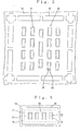
- Fig. 1 is a plan view illustrating an exemplary anisotropically conductive connector according to the present invention
- Fig. 2 is a plan view illustrating, on an enlarged scale, a part of the anisotropically conductive connector shown in Fig. 1
- Fig. 3 is a plan view illustrating, on an enlarged scale, an elastic anisotropically conductive film in the anisotropically conductive connector shown in Fig. 1
- Fig. 4 is a cross-sectional view illustrating, on an enlarged scale, the elastic anisotropically conductive film in the anisotropically conductive connector shown in Fig. 1.
- the anisotropically conductive connector shown in Fig. 1 is that used in conducting electrical inspection of each of, for example, a plurality of integrated circuits formed on a wafer in a state of the wafer and has a frame plate 10 in which a plurality of anisotropically conductive film-arranging holes 11 (indicated by broken lines) each extending through in a thickness-wise direction of the frame plate have been formed as illustrated in Fig. 2.
- the anisotropically conductive film-arranging holes 11 in this frame plate 10 are formed in accordance with a pattern of electrode regions, in which electrodes to be inspected have been formed in the integrated circuits formed on the wafer that is an object of inspection.
- Elastic anisotropically conductive films 20 having conductivity in the thickness-wise direction are arranged in the respective anisotropically conductive film-arranging holes 11 in the frame plate 10 in a state that they are each supported by the peripheral edge about the anisotropically conductive film-arranging hole 11 of the frame plate 10 and in a state independent of adjacent anisotropically conductive films 20 to each other.
- air circulating holes 15 for circulating air between the anisotropically conductive connector and a member adjacent thereto when a pressurizing means of a pressure reducing system is used in a wafer inspection apparatus, which will be described subsequently.
- positioning holes 16 for positioning between the wafer, which is the object of inspection, and a circuit board for inspection are formed.
- the elastic anisotropically conductive films 20 is formed by an elastic polymeric substance and, as illustrated in Fig. 3, has a functional part 21 composed of a plurality of conductive parts 22 for connection each extending in the thickness-wise direction (direction perpendicular to the paper in Fig. 3) of the film and an insulating part 23 formed around each of the conductive parts 22 for connection and mutually insulating these conductive parts 22 for connection.
- the functional part 21 is arranged so as to be located on the anisotropically conductive film-arranging hole 11 in the frame plate 10.
- the conductive parts 22 for connection in the functional part 21 are arranged in accordance with a pattern corresponding to a pattern of the electrodes to be inspected in the integrated circuit formed on the wafer, which is the object of inspection, and electrically connected to the electrodes to be inspected in the inspection of the wafer.
- a part 25 to be supported which is fixed to and supported by the periphery about the anisotropically conductive film-arranging hole 11 in the frame plate 10, is formed integrally and continuously with the functional part 21. More specifically, the part 25 to be supported in this embodiment is shaped in a forked form and fixed and supported in a closely contacted state so as to grasp the periphery about the anisotropically conductive film-arranging hole 11 in the frame plate 10.
- conductive particles P exhibiting magnetism are contained at a high density in a state oriented so as to align in the thickness-wise direction as illustrated in Fig. 4.
- the insulating part 23 does not contain the conductive particles P at all or scarcely contain them.
- the part 25 to be supported in the elastic anisotropically conductive film 20 contains the conductive particles P.
- projected parts 24 protruding from other surfaces than portions, at which the conductive parts 22 for connection and peripheries thereof are located, are formed at those portions on both sides of the functional part 21 in the elastic anisotropically conductive film 20.
- the thickness of the frame plate 10 varies according to the material thereof, but is preferably 20 to 600 ⁇ m, more preferably 40 to 400 ⁇ m.
- this thickness is less than 20 ⁇ m, the strength required upon use of the resulting anisotropically conductive connector is not achieved, and the durability thereof is liable to be lowered. In addition, such stiffness as the form of the frame plate is retained is not achieved, and the handling property of the anisotropically conductive connector becomes low. If the thickness exceeds 600 ⁇ m on the other hand, the elastic anisotropically conductive films 20 formed in the anisotropically conductive film-arranging holes 11 become too great in thickness, and it may be difficult in some cases to achieve good conductivity in the conductive parts 22 for connection and insulating property between adjoining conductive parts 22 for connection.
- the form and size in a plane direction of the anisotropically conductive film-arranging holes 11 in the frame plate 10 are designed according to the size, pitch and pattern of electrodes to be inspected in a wafer that is an object of inspection.
- the frame plate 10 As a material for forming the frame plate 10, no particular limitation is imposed so far as it has such stiffness as the resulting frame plate 10 is hard to be deformed, and the form thereof is stably retained, and for example, various kinds of materials such as metallic materials, ceramic materials and resin materials may be used.
- the frame plate 10 is formed by, for example, a metallic material, an insulating film may be formed on the surface of the frame plate 10.
- the metallic material for forming the frame plate 10 include metals such as iron, copper, nickel, chromium, cobalt, magnesium, manganese, molybdenum, indium, lead, palladium, titanium, tungsten, aluminum, gold, platinum and silver, and alloys or alloy steels composed of a combination of at least two of these metals.
- resin material forming the frame plate 10 include liquid crystal polymers and polyimide resins.
- the insulating film may be used a fluororesin film, a polyimide resin film, a composite film containing a fluororesin or polyimide resin, or a metal oxide film.
- the frame plate 10 may preferably exhibit magnetism at least at the peripheral portion about each of the anisotropically conductive film-arranging holes 11, i.e., a portion supporting the elastic anisotropically conductive film 20 in that the conductive particles P can be caused to be contained with ease in the part 25 to be supported in the elastic anisotropically conductive film 20 by a process which will be described subsequently.
- this portion may preferably have a saturation magnetization of at least 0.1 Wb/m 2 .
- the whole frame plate 10 may preferably be formed by a magnetic substance in that the frame plate 10 is easy to be produced.
- magnétique substance forming such a frame plate 10 include iron, nickel, cobalt, alloys of these magnetic metals, and alloys or alloy steels of these magnetic metals with any other metal.
- the resulting anisotropically conductive connector is used in the probe test or wafer level burn-in test, it is preferable to use a material having a coefficient of linear thermal expansion of at most 3 x 10 -5 /K, more preferably -1 x 10 -7 to 1 x 10 -5 /K, particularly preferably 1 x 10 -6 to 8 x 10 -6 /K as a material for forming the frame plate 10.
- invar alloys such as invar, Elinvar alloys such as Elinvar, and alloys or alloy steels of magnetic metals, such as superinvar, covar and 42 alloy.
- the overall thickness (thickness of the conductive parts 22 for connection in the illustrated embodiment) of the elastic anisotropically conductive film 20 is preferably 50 to 3,000 ⁇ m, more preferably 70 to 2,500 ⁇ m, particularly preferably 100 to 2,000 ⁇ m. When this thickness is 50 ⁇ m or greater, elastic anisotropically conductive films 20 having sufficient strength are provided with certainty. When this thickness is 3,000 ⁇ m or less on the other hand, conductive parts 22 for connection having necessary conductive properties are provided with certainty.
- the projected parts 24 are formed on both surfaces of the elastic anisotropically conductive film 20, respectively, but may be formed on only one surface of the elastic anisotropically conductive film 20.
- the projected height of such projected part 24 is preferably at least 10% in total of the thickness in the projected part 24, more preferably at least 20%. Projected parts 24 having such a projected height are formed, whereby the conductive parts 22 for connection are sufficiently compressed by small pressurizing force, so that good conductivity is surely achieved.
- the projected height of the projected part 24 is preferably at most 100%, more preferably at most 70% of the shortest width or diameter of the projected part 24. Projected parts 24 having such a projected height are formed, whereby the projected parts 24 are not buckled when they are pressurized, so that the expected conductivity is surely achieved.
- the thickness (thickness of one of the forked portions in the illustrated embodiment) of the part 25 to be supported is preferably 5 to 600 ⁇ m, more preferably 10 to 500 ⁇ m, particularly preferably 20 to 400 ⁇ m.
- part 25 it is not essential for the part 25 to be supported to be formed in the forked form, and it may be fixed to only one surface of the frame plate 10.
- the elastic polymeric substance forming the anisotropically conductive films 20 is preferably a heat-resistant polymeric substance having a crosslinked structure.
- Various materials may be used as curable polymeric substance-forming materials usable for obtaining such a crosslinked polymeric substance.
- liquid silicone rubber is preferred.
- the liquid silicone rubber may be any of addition type and condensation type. However, the addition type liquid silicone rubber is preferred.
- This addition type liquid silicone rubber is that cured by a reaction of a vinyl group with an Si-H bond and includes a one-pack type (one-component type) composed of polysiloxane having both vinyl group and Si-H bond and a two-pack type (two-component type) composed of polysiloxane having a vinyl group and polysiloxane having an Si-H bond.
- addition type liquid silicone rubber of the two-pack type is preferably used.
- the addition type liquid silicone rubber is used that having a viscosity of preferably 100 to 1,000 Pa ⁇ s, more preferably 150 to 800 Pa ⁇ s, particularly preferably 250 to 500 Pa ⁇ s at 23°C. If this viscosity is lower than 100 Pa ⁇ s, precipitation of the conductive particles in such addition type liquid silicone rubber is easy to occur in a molding material for obtaining the elastic anisotropically conductive films 20, which will be described subsequently, so that good storage stability is not obtained.
- the conductive particles are not oriented so as to align in the thickness-wise direction of the molding material layer when a parallel magnetic field is applied to the molding material layer, so that it may be difficult in some cases to form a chain of the conductive particles in an even state.
- the viscosity of such addition type liquid silicone rubber can be measured by means of a Brookfield type viscometer.
- the cured silicone rubber When the elastic anisotropically conductive films 20 are formed by a cured product (hereinafter referred to as "cured silicon rubber") of the liquid silicone rubber, the cured silicone rubber preferably has a compression set of at most 10%, more preferably at most 8%, still more preferably at most 6% at 150°C. If the compression set exceeds 10%, a chain of the conductive particles P in the conductive part 22 for connection is disordered when the resulting anisotropically conductive connector is used repeatedly under a high-temperature environment. As a result, it is difficult to retain the necessary conductivity.
- the compression set of the cured silicone rubber can be measured by a method in accordance with JIS K 6249.
- the cured silicone rubber forming the elastic anisotropically conductive films 20 preferably has a durometer A hardness of 10 to 60, more preferably 15 to 60, particularly preferably 20 to 60 at 23°C. If the durometer A hardness is lower than 10, the insulating part 23 mutually insulating the conductive parts 22 for connection is easily over-distorted when pressurized, and so it may be difficult in some cases to retain the necessary insulating property between the conductive parts 22 for connection. If the durometer A hardness exceeds 60 on the other hand, pressurizing force by a considerably heavy load is required for giving proper distortion to the conductive parts 22 for connection, so that, for example, a wafer, which is an object of inspection, tends to cause great deformation or breakage.
- the durometer A hardness of the cured silicone rubber can be measured by a method in accordance with JIS K 6249.
- the cured silicone rubber for forming the elastic anisotropically conductive films 20 preferably has tear strength of at least 8 kN/m, more preferably at least 10 kN/m, still more preferably at least 15 kN/m, particularly preferably at least 20 kN/m at 23°C. If the tear strength is lower than 8 kN/m, the resulting elastic anisotropically conductive films 20 tend to deteriorate durability when they are distorted in excess.
- the tear strength of the cured silicone rubber can be measured by a method in accordance with JIS K 6249.
- liquid silicone rubber having such properties may be used that marketed as liquid silicone rubber "KE2000” series, “KE1950” series or “KE1990” series from Shin-Etsu Chemical Co., Ltd.
- a proper curing catalyst may be used for curing the addition type liquid silicone rubber.
- a curing catalyst may be used a platinum-containing catalyst.
- Specific examples thereof include publicly known catalysts such as platinic chloride and salts thereof, platinum-unsaturated group-containing siloxane complexes, vinylsiloxane-platinum complexes, platinum-1,3-divinyltetramethyldisiloxane complexes, complexes of triorganophosphine or phosphite with platinum, acetyl acetate-platinum chelates, and cyclic diene-platinum complexes.
- the amount of the curing catalyst used is suitably selected in view of the kind of the curing catalyst and other curing treatment conditions. However, it is generally 3 to 15 parts by weight per 100 parts by weight of the addition type liquid silicone rubber.
- a general inorganic filler such as silica powder, colloidal silica, aerogel silica or alumina may be contained in the addition type liquid silicone rubber as needed.
- the conductive particles P contained in the conductive parts 22 for connection and the parts 25 to be supported in each of the elastic anisotropically conductive films 20 are used particles obtained by forming one or more coating layers composed of a high-conductive metal on the surfaces of core particles (hereinafter also referred to as “magnetic core particles") exhibiting magnetism.
- core particles hereinafter also referred to as “magnetic core particles”
- high-conductive metal means a metal having an electric conductivity of at least 5 x 10 6 ⁇ -1 m -1 at 0°C.
- the magnetic core particles for obtaining the conductive particles P preferably have a number average particle diameter of 3 to 50 ⁇ m.
- the number average particle diameter of the magnetic core particles means a value measured by a laser diffraction scattering method.
- conductive parts 22 for connection When the number average particle diameter is 3 ⁇ m or greater, conductive parts 22 for connection, which are easy to be deformed under pressure, low in resistance value and high in connection reliability can be easily obtained. When the number average particle diameter is 50 ⁇ m or smaller on the other hand, fine conductive parts 22 for connection can be easily formed, and the resultant conductive parts 22 for connection tend to have stable conductivity.
- the magnetic core particles preferably have a BET specific surface area of 10 to 1,500 m 2 /kg, more preferably 20 to 1,000 m 2 /kg, particularly preferably 50 to 500 m 2 /kg.
- the BET specific surface area is 10 m 2 /kg or wider, plating can be surely conducted on such magnetic core particles in a necessary amount because such magnetic core particles have a sufficiently wide area capable of being plated. Accordingly, conductive particles P high in conductivity can be obtained, and stable and high conductivity is achieved because a contact area between the conductive particles P is sufficiently wide.
- the BET specific surface area is 1,500 m 2 /kg or smaller on the other hand, such magnetic core particles do not become brittle, so that they are seldom broken when physical stress is applied, and so stable and high conductivity is retained.
- the magnetic core particles preferably have a coefficient of variation of particle diameter of at most 50%, more preferably at most 40%, still more preferably at most 30%, particularly preferably at most 20%.
- the coefficient of variation of particle diameter is a value determined in accordance with an expression: ( ⁇ /Dn) x 100, wherein ⁇ is a standard deviation value of the particle diameter, and Dn is a number average particle diameter of the particles.
- conductive parts 22 for connection which are narrow in scatter of conductivity, can be formed because the evenness of particle diameter is high.
- a material for forming the magnetic core particles may be used iron, nickel, cobalt, a material obtained by coating copper or a resin with such a metal, or the like.
- those having a saturation magnetization of at least 0.1 Wb/m 2 may be preferably used.
- the saturation magnetization thereof is more preferably at least 0.3 Wb/m 2 , particularly preferably 0.5 Wb/m 2 .
- Specific examples of the material include iron, nickel, cobalt and alloys thereof.
- the conductive particles P can be easily moved in the molding material layers for forming the elastic anisotropically conductive films 20 by a process, which will be described subsequently, whereby the conductive particles P can be surely moved to portions to become conductive parts for connection in the respective molding material layers to form chains of the conductive particles P.
- the coating layer in the conductive particles P is composed of one layer in the present invention
- such a coating layer has a high hardness of, for example, at least 40, preferably at least 50 in terms of a Vickers hardness (Hv).
- the coating layer in the conductive particles P is composed of 2 or more layers, at least the outermost coating layer (hereinafter referred to as "surface coating layer”) among them has a high hardness of, for example, at least 40, preferably at least 150 in terms of a Vickers hardness (Hv).
- Such a coating layer may be formed by a single metal or 2 or more metals.
- the coating layer may be that formed of an alloy of a metal having a Vickers hardness (Hv) of at least 40 and another metal than such a metal, for example, gold or that having a phase-separation structure that a metal phase composed of a metal having a Vickers hardness (Hv) of at least 40 is dispersed in a metal phase composed of another metal than such a metal, for example, gold so far as the coating layer has a Vickers hardness (Hv) of at least 40 as a whole.
- the high-conductive metal having a Vickers hardness (Hv) of at least 40 may be used palladium, rhodium, ruthenium, iridium, platinum, tungsten, nickel, cobalt, chromium or an alloy thereof.
- palladium, rhodium, ruthenium, iridium and platinum may preferably be used in that they are chemically stable and have a high electric conductivity.
- the alloy of the metal having a Vickers hardness (Hv) of at least 40 and gold may be used a gold-palladium alloy, a gold-copper alloy, a platinum-gold alloy, hard gold containing 0.1 to 1.0% of nickel or cobalt, or the like.
- the gold-palladium alloy and the hard gold containing 0.1 to 1.0% of nickel or cobalt may preferably be used in that they are chemically stable and have a high electric conductivity.
- the metal forming any other coating layer (hereinafter referred to as "intermediate coating layer") than the surface coating layer.
- intermediate coating layer any other coating layer (hereinafter referred to as "intermediate coating layer") than the surface coating layer.
- silver, copper and gold may preferably be used in that they have exceptionally high conductivity, with gold being particularly preferred in that it is chemically stable.
- a proportion [(mass of coating layer/mass of core particles) x 100] of the mass (in the case where the conductive particles have the coating layer of 2 or more layers, a total mass thereof) of the coating layer to the mass of the core particles is preferably at least 15% by mass, more preferably 25 to 35% by mass.
- the proportion of the mass of the coating layer is lower than 15% by mass, the conductivity of such conductive particles P is markedly deteriorated when the resulting anisotropically conductive connector is used repeatedly under a high-temperature environment, and so it may be difficult in some cases to retain the necessary conductivity.
- the thickness t of the coating layer is preferably at least 40 nm, more preferably 100 to 200 nm.
- t [1/(Sw ⁇ )] x [N/ (1 - N)] wherein t is the thickness (m) of the coating layer, Sw is a BET specific surface area (m 2 /kg) of the core particles, ⁇ is a specific gravity (kg/m 3 ) of the metal forming the coating layer, and N is a value of (mass of the coating layer/total mass of the conductive particles).
- this thickness t of the coating layer is at least 40 nm, the conductivity of such conductive particles P is not markedly lowered, in the case where the resulting anisotropically conductive connector is used repeatedly under a high-temperature environment, because the high-conductive metal exists in a high proportion on the surfaces of the conductive particles P even when the substance forming the magnetic core particles and the substance forming the electrodes to be inspected migrate into the coating layer. Thus, the expected conductivity is retained.
- the BET specific surface area of the conductive particles P is preferably 10 to 1,500 m 2 /kg.
- this BET specific surface area is 10 m 2 /kg or wider, the surface area of the coating layer becomes sufficiently wide, so that the coating layer great in the overall weight of the high-conductive metal can be formed. Accordingly, particles high in conductivity can be provided. In addition, stable and high conductivity can be achieved because a contact area among the conductive particles P is sufficiently wide.
- this BET specific surface area is 1,500 m 2 /kg or smaller on the other hand, such conductive particles do not become brittle, and thus they are not broken even when physical stress is applied thereto, and so the stable and high conductivity is retained.
- the number average particle diameter of the conductive particles P is preferably 3 to 50 ⁇ m, more preferably 6 to 15 ⁇ m.
- Such conductive particles P are used, whereby the resulting elastic anisotropically conductive films 20 become easy to be deformed under pressure. In addition, sufficient electrical contact is achieved between the conductive particles P in the conductive parts 22 for connection in the elastic anisotropically conductive films 20.
- the conductive particles P are preferably in the shape of a sphere or star, or lump by secondary particles obtained by aggregating these particles from the viewpoint of permitting easy dispersion of these particles in the polymeric substance-forming material.
- the electric resistance value R is preferably at most 0.3 ⁇ , more preferably at most 0.1 ⁇ .
- Electric resistance value R an electric resistance value determined by preparing a paste composition by kneading 6 g of the conductive particles and 8 g of liquid rubber, arranging this paste composition between a pair of electrodes arranged at a clearance of 0.5 mm so as to oppose to each other and each having a diameter of 1 mm, applying a magnetic field of 0.3 T between the pair of the electrodes, and leaving those to stand in this state until the electric resistance value between the pair of the electrodes becomes stable.
- the electric resistance value R is measured in the following manner.
- Fig. 5 illustrates an apparatus for measuring an electric resistance value R.
- Reference numeral 71 indicates a ceramic cell in which a sample chamber S is formed, and the cell is constructed by a cylindrical side wall material 72 and a pair of lid members 73 each having a through-hole 73H at its center.
- Reference numeral 74 designates a pair of conductive magnets each having an electrode part 75, which is in the form protruding from the surface thereof and fitted to the through-hole 73H in the lid member 73. Each magnet is fixed to the lid member 73 in a state that the electrode part 75 has been fitted into the through-hole 73H in the lid member 73.
- Reference numeral 76 indicates an electric resistance meter connected to each of the pair of the magnets 74.
- the sample chamber S of the cell 71 is in the form of a disk having a diameter d1 of 3 mm and a thickness d2 of 0.5 mm, and the inner diameter of the through-hole 73H in the lid member 73, i.e., the diameter r of the electrode part 75 of the magnet 74 is 1 mm.
- the paste composition described above is filled into the sample chamber S of the cell 71, and an electric resistance value between the electrodes 75 of the magnets 74 is measured by the electric resistance meter 76 while applying a parallel magnetic field of 0.3 T between the electrodes 75 of the magnets 74 in the thickness-wise direction of the sample chamber S.
- the conductive particles dispersed in the paste composition are gathered between the electrodes 75 of the magnets 74 by the effect of the parallel magnetic field and oriented so as to align in the thickness-wise direction.
- the electric resistance value between the electrodes 75 of the magnets 74 lowers and then becomes a stable state, thereby measuring an electric resistance value at this time.
- the duration of time from the time the parallel magnetic field has been applied to the paste composition up to the time the electric resistance value between the electrodes 75 of the magnets 74 has reached the stable state varies according to the kind of the conductive particles.
- an electric resistance value after 500 seconds have elapsed from the application of the parallel magnetic field to the paste composition is generally measured as the electric resistance value R.
- the water content in the conductive particles P is preferably at most 5% by mass, more preferably at most 3% by mass, still more preferably at most 2% by mass, particularly preferably at most 1% by mass.
- the conductive particles P may be those treated with a coupling agent such as a silane coupling agent on surfaces thereof.
- a coupling agent such as a silane coupling agent
- the adhesion property of the conductive particles P to the elastic polymeric substance is enhanced. As a result, a conductive material high in durability is obtained.
- the amount of the coupling agent used is suitably selected within limits not affecting the conductivity of the conductive particles P. However, it is preferably such an amount that a coating rate (proportion of an area coated with the coupling agent to the surface area of the conductive particles) of the coupling agent on the surfaces of the conductive particles P amounts to at least 5%, more preferably 7 to 100%, still more preferably 10 to 100%, particularly preferably 20 to 100%.
- Such conductive particles P may be obtained in accordance with, for example, the following process.
- Particles are first formed from a ferromagnetic material in accordance with a method known per se in the art, or commercially available particles of a ferromagnetic substance are provided. The particles are subjected to a classification treatment to prepare magnetic core particles having a necessary particle diameter.
- the classification treatment of the particles can be conducted by means of, for example, a classifier such as an air classifier or sonic classifier.
- Specific conditions for the classification treatment are suitably preset according to the intended number average particle diameter of the magnetic core particles, the kind of the classifier, and the like.
- the magnetic core particles are then subjected to a surface oxide film-removing treatment and further to a surface-washing treatment with, for example, purified water, thereby removing impurities such as dirt, foreign matter and oxide films, which are present on the surfaces of the magnetic core particles.
- a coating layer composed of the high-conductive metal is formed on the surfaces of the magnetic core particles.
- the thus-treated particles are further subjected to a classification treatment as needed, thereby obtaining conductive particles.
- a specific method of the surface oxide film-removing treatment for the magnetic core particles may be used a treatment method with an acid such as hydrochloric acid.
- the anti-oxidizing treatment for the magnetic core particles may be used a treatment method with water-soluble fullerene or the like.
- a wet process such as an electroless plating process such as a displacement plating process or chemical reduction plating process, or an electroplating process, or a dry process such as a sputtering process or vapor deposition process may be used.
- the electroless plating process, electroplating process and sputtering process may preferably be used.
- a process for forming the coating layer by the electroless plating process such as the chemical reduction plating process or displacement plating process will be described.
- the magnetic core particles subjected to the acid treatment and washing treatment are first added to a plating solution to prepare a slurry, and electroless plating on the magnetic core particles is conducted while stirring the slurry.
- the particles in the slurry are then separated from the plating solution. Thereafter, the particles separated are subjected to a washing treatment with, for example, purified water, thereby obtaining conductive particles with a coating layer composed of the high-conductive metal formed on the surfaces of the magnetic core particles.
- an intermediate coating layer be formed on the surfaces of the magnetic core particles by, for example, the electroless plating process, and a surface coating layer be then formed on the surface of the intermediate coating layer by electroplating process.
- plating solution used in the electroless plating process No particular limitation is imposed on the plating solution used in the electroless plating process, and various kinds of commercially available plating solutions may be used.
- the resultant conductive particles are preferably subjected to a classification treatment as needed.
- a classification treatment By the classification treatment, conductive particles having the expected particle diameter can be surely obtained.
- classifier used for conducting the classification treatment for the conductive particles may be mentioned those exemplified as the classifier used in the classification treatment for preparing the magnetic core particles.
- a proportion of the conductive particles P contained in the conductive parts 22 for connection in the functional part 21 is preferably 10 to 60%, more preferably 15 to 50% in terms of volume fraction. If this proportion is lower than 10%, it may be impossible in some cased to obtain conductive parts 22 for connection sufficiently low in electric resistance value. If this proportion exceeds 60% on the other hand, the resulting conductive parts 22 for connection are liable to be brittle, so that elasticity required of the conductive parts 22 for connection may not be achieved in some cases.
- a proportion of the conductive particles P contained in the parts 25 to be supported varies according to the content of the conductive particles in the molding material for forming the elastic anisotropically conductive films 20. However, it is preferably equivalent to or higher than the proportion of the conductive particles contained in the molding material in that the conductive particles P are surely prevented from being contained in excess in the conductive parts 22 for connection located most outside among the conductive parts 22 for connection in the elastic anisotropically conductive film 20. It is also preferably at most 30% in terms of volume fraction in that parts 25 to be supported having sufficient strength are provided.
- the anisotropically conductive connector described above may be produced, for example, in the following manner.
- a method for forming the anisotropically conductive film-arranging holes 11 in the frame plate 10 may be used, for example, an etching method or the like.
- a mold 60 for molding elastic anisotropically conductive films is provided, and the conductive paste composition as a molding material for elastic anisotropically conductive films is applied to the respective molding surfaces of a top force 61 and a bottom force 65 in the mold 60 in accordance with a necessary pattern, i.e., an arrangement pattern of elastic anisotropically conductive films to be formed, thereby forming molding material layers 20A.
- the mold 60 will be described specifically. This mold 60 is constructed by arranging the top force 61 and the bottom force 65 making a pair therewith so as to oppose to each other.
- ferromagnetic substance layers 63 are formed on a lower surface of a base plate 62 in accordance with a pattern antipodal to an arrangement pattern of conductive parts 22 for connection in elastic anisotropically conductive films 20 to be molded, and a non-magnetic substance layer 64 is formed at another portion than the ferromagnetic substance layers 63.
- the molding surface is formed by these ferromagnetic substance layers 63 and non-magnetic substance layer 64.
- Recessed parts 64a are formed in the molding surface of the top force 61 corresponding to the projected parts 24 in the elastic anisotropically conductive films 20 to be molded.
- ferromagnetic substance layers 67 are formed on an upper surface of a base plate 66 in accordance with the same pattern as the arrangement pattern of the conductive parts 22 for connection in the elastic anisotropically conductive films 20 to be molded, and a non-magnetic substance layer 68 is formed at another portion than the ferromagnetic substance layers 67.
- the molding surface is formed by these ferromagnetic substance layers 67 and non-magnetic substance layer 68.
- Recessed parts 68a are formed in the molding surface of the bottom force 65 corresponding to the projected parts 24 in the elastic anisotropically conductive films 20 to be molded.
- the respective base plates 62 and 66 in the top force 61 and bottom force 65 are preferably formed by a ferromagnetic substance.
- a ferromagnetic substance include ferromagnetic metals such as iron, iron-nickel alloys, iron-cobalt alloys, nickel and cobalt.
- the base plates 62, 66 preferably have a thickness of 0.1 to 50 mm, and surfaces thereof are preferably smooth and subjected to a chemical degreasing treatment and/or mechanical polishing treatment.
- a ferromagnetic metal such as iron, iron-nickel alloy, iron-cobalt alloy, nickel or cobalt.
- the ferromagnetic substance layers 63, 67 preferably have a thickness of at least 10 ⁇ m. When this thickness is at least 10 ⁇ m, a magnetic field having a sufficient intensity distribution can be applied to the molding material layers 20A. As a result, the conductive particles can be gathered at a high density to portions to become conductive parts 22 for connection in the molding material layers 20A, and so conductive parts 22 for connection having good conductivity can be provided.
- non-magnetic substance layers 64, 68 in both top force 61 and bottom force 65 may be used a non-magnetic metal such as copper, a polymeric substance having heat resistance, or the like.
- a polymeric substance cured by radiation may preferably be used in that the non-magnetic substance layers 64, 68 can be easily formed by a technique of photolithography.
- a photoresist such as an acrylic type dry film resist, epoxy type liquid resist or polyimide type liquid resist.
- a method for applying the molding material to the molding surfaces of the top force 61 and bottom force 65 may preferably be used a screen printing method. According to such a method, the molding material can be easily applied according to a necessary pattern, and a proper amount of the molding material can be applied.
- the frame plate 10 is then arranged in alignment on the molding surface of the bottom force 65, on which the molding material layers 20A have been formed, through a spacer 69a, and on the frame plate 10, the top force 61, on which the molding material layers 20A have been formed, is arranged in alignment through a spacer 69b.
- These top and bottom forces are superimposed on each other, whereby molding material layers 20A of the intended form (form of the elastic anisotropically conductive films 20 to be formed) are formed between the top force 61 and the bottom force 65 as illustrated in Fig. 9.
- the conductive particles P are contained in a state dispersed throughout in the molding material layer 20A as illustrated in Fig. 10.
- the spacers 69a and 69b are arranged between the frame plate 10, and the bottom force 65 and the top force 61, respectively, whereby the elastic anisotropically conductive films of the intended form can be formed, and adjoining elastic anisotropically conductive films are prevented from being connected to each other, so that a great number of anisotropically conductive films independent of one another can be formed with certainty.
- a pair of, for example, electromagnets are then arranged on the upper surface of the base plate 62 in the top force 61 and the lower surface of the base plate 66 in the bottom force 65, and the electromagnets are operated, whereby a magnetic field having higher intensity at portions between the ferromagnetic substance layers 63 of the top force 61 and their corresponding ferromagnetic substance layers 67 of the bottom force 65 than surrounding regions thereof is formed because the top force 61 and bottom force 65 have the ferromagnetic substance layers 63 and 67, respectively.
- the conductive particles P dispersed in the molding material layers 20A are gathered to portions to become the conductive parts 22 for connection, which are located between the ferromagnetic substance layers 63 of the top force 61 and their corresponding ferromagnetic substance layers 67 of the bottom force 65, and oriented so as to align in the thickness-wise direction of the molding material layers as illustrated in Fig. 11.
- the frame plate 10 is composed of the magnetic metal, a magnetic field having higher intensity at portions between the top force 61 and the bottom force 65, and the frame plate 10 than vicinities thereof is formed.
- the conductive particles P existing above and below the frame plate 10 in the molding material layers 20A are not gathered between the ferromagnetic substance layers 63 of the top force 61 and the ferromagnetic substance layers 67 of the bottom force 65, but remain retained above and below the frame plate 10.
- the molding material layers 20A are subjected to a curing treatment, whereby the elastic anisotropically conductive films 20 each composed of a functional part 21, in which a plurality of conductive parts 22 for connection containing the conductive particles P in the elastic polymeric substance in a state oriented so as to align in the thickness-wise direction are arranged in a state mutually insulated by an insulating part 23 composed of the elastic polymeric substance, in which the conductive particles P are not present at all or scarcely present, and a part 25 to be supported, which is continuously and integrally formed at a peripheral edge of the functional part 21 and in which the conductive particles P are contained in the elastic polymeric substance, are formed in a state that the part 25 to be supported has been fixed to the periphery about each anisotropically conductive film-arranging hole 11 of the frame plate 10, thus producing an anisotropically conductive connector.
- the intensity of the external magnetic field applied to the portions to become the conductive parts 22 for connection and the portions to become the parts 25 to be supported in the molding material layers 20A is preferably an intensity that it amounts to 0.1 to 2.5 T on the average.
- the curing treatment of the molding material layers 20A is suitably selected according to the material used. However, the treatment is generally conducted by a heating treatment. When the curing treatment of the molding material layers 20A is conducted by heating, it is only necessary to provide a heater to an electromagnet. Specific heating temperature and heating time are suitably selected in view of the kinds of the polymeric substance-forming material for forming the molding material layers 20A, and the like, the time required for movement of the conductive particles P, and the like.
- the conductive particles P contained in the conductive parts 22 for connection in the elastic anisotropically conductive films 20 are obtained by forming a coating layer having a Vickers hardness (Hv) of at least 40, so that occurrence of separation, abrasion, deformation and/or the like on the coating layer in the conductive particles P by contact between the conductive particles P, and the like is inhibited even when it is used repeatedly over a great number of times in electrical inspection of, for example, integrated circuits formed on wafer.
- Hv Vickers hardness
- Those composed of gold and another high-conductive metal are used as the conductive particles P, whereby conductive parts for connection having high conductivity are obtained, and moreover the surfaces of the conductive particles are inhibited from being deteriorated even when the anisotropically conductive connector is used repeatedly over a great number of times under a high-temperature environment. As a result, necessary conductivity is retained over a long period of time, and thus high durability and long service life are achieved.
- the proportion of the mass of the coating layer 20 to the mass of the core particles is at least 15% by mass, and the thickness t of the coating layer formed of the high-conductive metal is at least 40 nm are used as the conductive particles P, whereby, in the case where the anisotropically conductive connector is used repeatedly under a high-temperature environment, the conductivity of such conductive particles P is not markedly lowered because the high-conductive metal exists in a high proportion on the surfaces of the conductive particles P even when the substance forming the magnetic core particles and a substance forming electrodes to be inspected migrate into the coating layer. As a result, necessary conductivity is retained over a long period of time, and thus high durability and long service life are achieved.
- the anisotropically conductive connector is hard to be deformed and easy to handle, so that the positioning and the holding and fixing to a wafer, which is an object of inspection, can be easily conducted in an electrically connecting operation to the wafer.
- the respective anisotropically conductive film-arranging holes 11 in the frame plate 10 are formed corresponding to electrode regions, in which electrodes to be inspected have been formed, of integrated circuits in a wafer, which is an object of inspection, and the elastic anisotropically conductive film 20 arranged in each of the anisotropically conductive film-arranging holes 11 may be small in area, the individual elastic anisotropically conductive films 20 are easy to be formed.
- the elastic anisotropically conductive film 20 small in area is little in the absolute quantity of thermal expansion in a plane direction of the elastic anisotropically conductive film 20 even when it is subjected to thermal hysteresis, the thermal expansion of the elastic anisotropically conductive film 20 in the plane direction is surely restrained by the frame plate by using a material having a low coefficient of linear thermal expansion as that for forming the frame plate 10. Accordingly, a good electrically connected state can be stably retained even when the WLBI test or probe test is performed on a large-area wafer.
- That exhibiting magnetism is used as the frame plate 10, whereby the curing treatment of the molding material layers 20A can be conducted in the formation of the elastic anisotropically conductive films 20 in a state that the conductive particles P have been existed in the portions to become the parts 25 to be supported in the molding material layers 20A by applying, for example, a magnetic field to said portions, so that the conductive particles P existing in the portions to become the parts 25 to be supported in the molding material layers 20A, i.e., the portions located above and below the peripheries about the anisotropically conductive film-arranging holes 11 in the frame plate 10 are not gathered to the portions to become the conductive parts 22 for connection.
- the conductive particles P are surely prevented from being contained in excess in the conductive parts 22 for connection located most outside among the conductive parts 22 for connection in the elastic anisotropically conductive film 20. Accordingly, there is no need to reduce the content of the conductive particles P in the molding material layers 20A, so that good conductivity is surely achieved as to all the conductive parts 22 for connection, and insulating property between adjoining conductive parts 22 for connection is surely attained.
- positioning holes 16 are formed in the frame plate 10, positioning to the wafer, which is the object of inspection, or the circuit board for inspection can be easily conducted.
- air existing between the anisotropically conductive connector and the circuit board for inspection is discharged through the air circulating holes 15 in the frame plate 10 at the time the pressure within a chamber is reduced when that by the pressure reducing system is utilized as the means for pressing the probe member in a wafer inspection apparatus, which will be described subsequently, whereby the anisotropically conductive connector can be surely brought into close contact with the circuit board for inspection, so that the necessary electrical connection can be achieved with certainty.
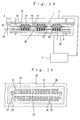
- Fig. 12 is a cross-sectional view schematically illustrating the construction of an exemplary wafer inspection apparatus making use of the anisotropically conductive connector according to the present invention.
- This wafer inspection apparatus serves to perform electrical inspection of each of a plurality of integrated circuits formed on a wafer in a state of the wafer.
- the wafer inspection apparatus shown in Fig. 12 has a probe member 1 for conducting electrical connection of each of electrodes 7 to be inspected of a wafer 6, which is an object of inspection, to a tester.
- the probe member 1 has a circuit board 30 for inspection, on the front surface (lower surface in the figure) of which a plurality of inspection electrodes 31 have been formed in accordance with a pattern corresponding to a pattern of the electrodes 7 to be inspected of the wafer 6 that is the object of inspection.
- On the front surface of the circuit board 30 for inspection is provided the anisotropically conductive connector 2 of the construction illustrated in Figs.
- a sheet-like connector 40 On the front surface (lower surface in the figure) of the anisotropically conductive connector 2 is provided a sheet-like connector 40, in which a plurality of electrode structures 42 have been arranged in an insulating sheet 41 in accordance with the pattern corresponding to the pattern of the electrodes 7 to be inspected of the wafer 6, which is the object of inspection, in such a manner that the electrode structures 42 are opposed to and brought into contact with the conductive parts 22 for connection in the elastic anisotropically conductive films 20 of the anisotropically conductive connector 2, respectively.
- a base material for making up the circuit board 30 for inspection may be used any of conventionally known various base materials. Specific examples thereof include composite resin materials such as glass fiber-reinforced epoxy resins, glass fiber-reinforced phenol resins, glass fiber-reinforced polyimide resins and glass fiber-reinforced bismaleimidotriazine resins, and ceramic materials such as glass, silicon dioxide and alumina.
- composite resin materials such as glass fiber-reinforced epoxy resins, glass fiber-reinforced phenol resins, glass fiber-reinforced polyimide resins and glass fiber-reinforced bismaleimidotriazine resins, and ceramic materials such as glass, silicon dioxide and alumina.
- Such a base material include Pyrex (Registered trademark) glass, quartz glass, alumina, beryllia, silicon carbide, aluminum nitride and boron nitride.
- This sheet-like connector 40 in the probe member 1 will be described specifically.
- This sheet-like connector 40 has a flexible insulating sheet 41, and in this insulating sheet 41, a plurality of electrode structures 42 extending in the thickness-wise direction of the insulating sheet 41 and composed of a metal are arranged in a state separated from each other in a plane direction of the insulating sheet 41 in accordance with the pattern corresponding to the pattern of the electrodes 7 to be inspected of the wafer 6 that is the object of inspection.
- Each of the electrode structures 42 is formed by integrally connecting a projected front-surface electrode part 43 exposed to the front surface (lower surface in the figure) of the insulating sheet 41 and a plate-like back-surface electrode part 44 exposed to the back surface of the insulating sheet 41 to each other by a short circuit part 45 extending through in the thickness-wise direction of the insulating sheet 41.
- the insulating sheet 41 has insulating property and is flexible.
- a resin sheet formed of a polyimide resin, liquid crystal polymer, polyester, fluororesin or the like, or a sheet obtained by impregnating a cloth woven by fibers with any of the above-described resins may be used.
- the thickness of the insulating sheet 41 is flexible. However, it is preferably 10 to 50 ⁇ m, more preferably 10 to 25 ⁇ m.
- the electrode structures 42 may be used nickel, copper, gold, silver, palladium, iron or the like.
- the electrode structures 42 may be any of those formed of a single metal as a whole, those formed of an alloy of at least two metals and those obtained by laminating at least two metals.
- a film of a chemically stable metal having high conductivity, such as gold, silver or palladium is preferably formed in that oxidation of the electrode parts is prevented, and electrode parts small in contact resistance are obtained.
- the projected height of the front-surface electrode part 43 in the electrode structure 42 is preferably 15 to 50 ⁇ m, more preferably 15 to 30 ⁇ m in that stable electrical connection to the electrode 7 to be inspected of the wafer 6 can be achieved.
- the diameter of the front-surface electrode part 43 is preset according to the size and pitch of the electrodes to be inspected of the wafer 6 and is, for example, 30 to 80 ⁇ m, preferably 30 to 50 ⁇ m.
- the diameter of the back-surface electrode part 44 in the electrode structure 42 is only necessary for the diameter of the back-surface electrode part 44 in the electrode structure 42 to be greater than the diameter of the short circuit part 45 and smaller than the arrangement pitch of the electrode structures 42, and the diameter is preferably great as much as possible, whereby stable electrical connection to the conductive part 22 for connection in the elastic anisotropically conductive film 20 of the anisotropically conductive connector 2 can also be achieved with certainty.
- the thickness of the back-surface electrode part 44 is preferably 20 to 50 ⁇ m, more preferably 30 to 40 ⁇ m in that sufficiently high strength and excellent repetitive durability are achieved.
- the diameter of the short circuit part 45 in the electrode structure 42 is preferably 30 to 80 ⁇ m, more preferably 30 to 50 ⁇ m in that sufficiently high strength is achieved.
- the sheet-like connector 40 can be produced, for example, in the following manner.
- a laminate material obtained by laminating a metal layer on an insulating sheet 41 is provided, and a plurality of through-holes extending through in the thickness-wise direction of the insulating sheet 41 are formed in the insulating sheet 41 of the laminate material in accordance with a pattern corresponding to a pattern of electrode structures 42 to be formed by laser machining, dry etch machining or the like.
- This laminate material is then subjected to photolithography and a plating treatment, whereby short circuit parts 45 integrally connected to the metal layer are formed in the through-holes in the insulating sheet 41, and at the same time, projected front-surface electrode parts 43 integrally connected to the respective short circuit parts 45 are formed on a front surface of the insulating sheet 41.
- the metal layer of the laminate material is subjected to a photo-etching treatment to remove a part thereof, thereby forming back-surface electrode parts 44 to form the electrode structures 42, thus obtaining the sheet-like connector 40.
- a wafer 6, which is an object of inspection is mounted on the wafer mounting table 4, and the probe member 1 is then pressurized downward by the pressurizing plate 3, whereby the respective front-surface electrode parts 43 in the electrode structures 42 of the sheet-like connector 40 thereof are brought into contact with their corresponding electrodes 7 to be inspected of the wafer 6, and moreover the respective electrodes 7 to be inspected of the wafer 6 are pressurized by the front-surface electrodes parts 43.
- the conductive parts 22 for connection in the elastic anisotropically conductive films 20 of the anisotropically conductive connector 2 are respectively held and pressurized by the inspection electrodes 31 of the circuit board 30 for inspection and the front-surface electrode parts 43 of the electrode structures 42 of the sheet-like connector 40 and compressed in the thickness-wise direction of the elastic anisotropically conductive films 20, whereby conductive paths are formed in the respective conductive parts 22 for connection in the thickness-wise direction thereof.
- electrical connection between the electrodes 7 to be inspected of the wafer 6 and the inspection electrodes 31 of the circuit board 30 for inspection is achieved.
- the wafer 6 is heated to a predetermined temperature through the wafer mounting table 4 and the pressurizing plate 3 by the heater 5. In this state, necessary electrical inspection is performed on each of a plurality of integrated circuits in the wafer 6.
- a wafer inspection apparatus it is equipped with the probe member 1 having the anisotropically conductive connector 2 high in durability and long in service life, so that the frequency of replacing the anisotropically conductive connector 2 by a new one can be reduced, whereby the inspection of wafers can be conducted at high efficiency, and the inspection cost can be reduced.
- positioning, and holding and fixing to the wafer can be conducted with ease even when the pitch of the electrodes 7 to be inspected is small, and moreover the necessary electrical inspection can be stably performed over a long period of time even when the apparatus is used repeatedly under a high-temperature environment.
- each of the elastic anisotropically conductive films 20 in the anisotropically conductive connector 2 is small in its own area, and the absolute quantity of thermal expansion in a plane direction of the elastic anisotropically conductive film 20 is little even when it is subjected to thermal hysteresis, the thermal expansion of the elastic anisotropically conductive film 20 in the plane direction is surely restrained by the frame plate by using a material having a low coefficient of linear thermal expansion as that for forming the frame plate 10. Accordingly, a good electrically connected state can be stably retained even when the WLBI test is performed on a large-area wafer.
- Fig. 14 is a cross-sectional view schematically illustrating the construction of another exemplary wafer inspection apparatus making use of the anisotropically conductive connector according to the present invention.
- This wafer inspection apparatus has a box-type chamber 50 opened at the top thereof, in which a wafer 6 that is an object of inspection is housed.
- An evacuation pipe 51 for evacuating air within the chamber 50 is provided in a sidewall of this chamber 50, and an evacuator (not illustrated) such as, for example, a vacuum pump, is connected to the evacuation pipe 51.
- a probe member 1 of the same construction as the probe member 1 in the wafer inspection apparatus shown in Fig. 12 is arranged on the chamber 50 so as to air-tightly close the opening of the chamber 50. More specifically, an elastic 0-ring 55 is arranged in close contact on an upper end surface of the sidewall in the chamber 50, and the probe member 1 is arranged in a state that the anisotropically conductive connector 2 and sheet-like connector 40 thereof have been housed in the chamber 50, and the periphery of the circuit board 30 for inspection thereof has been brought into close contact with the O-ring 55. Further, the circuit board 30 for inspection is held in a state pressurized downward by a pressurizing plate 3 provided on the back surface (upper surface in the figure) thereof.
- a heater 5 is connected to the chamber 50 and the pressurizing plate 3.
- the evacuator connected to the evacuation pipe 51 of the chamber 50 is driven, whereby the pressure within the chamber 50 is reduced to, for example, 1,000 Pa or lower.
- the probe member 1 is pressurized downward by the atmospheric pressure, whereby the 0-ring 55 is elastically deformed, and so the probe member 1 is moved downward.
- electrodes 7 to be inspected of the wafer 6 are respectively pressurized by their corresponding front-surface electrode parts 43 in electrode structures 42 of the sheet-like connector 40.
- the conductive parts 22 for connection in the elastic anisotropically conductive films 20 of the anisotropically conductive connector 2 are respectively held and pressurized by the inspection electrodes 31 of the circuit board 30 for inspection and the front-surface electrode parts 43 in the electrode structures 42 of the sheet-like connector 40 and compressed in the thickness-wise direction, whereby conductive paths are formed in the respective conductive parts 22 for connection in the thickness-wise direction thereof.
- electrical connection between the electrodes 7 to be inspected of the wafer 6 and the inspection electrodes 31 of the circuit board 30 for inspection is achieved.
- the wafer 6 is heated to a predetermined temperature through the chamber 50 and the pressurizing plate 3 by the heater 5. In this state, necessary electrical inspection is performed on each of a plurality of integrated circuits in the wafer 6.
- the whole inspection apparatus can be miniaturized because any large-sized pressurizing mechanism is not required, and moreover the whole wafer 6, which is the object of inspection, can be pressed by even force even when the wafer 6 has a large area of, for example, 8 inches or greater in diameter.
- the air circulating holes 15 are formed in the frame plate 10 in the anisotropically conductive connector 2, air existing between the anisotropically conductive connector 2 and the circuit board 30 for inspection is discharged through the air circulating holes 15 of the frame plate 10 in the anisotropically conductive connector 2 when the pressure within the chamber 50 is reduced, whereby the anisotropically conductive connector 2 can be surely brought into close contact with the circuit board 30 for inspection, so that the necessary electrical connection can be achieved with certainty.
- inspection time required of each of integrated circuits is as long as several hours, and so high time efficiency can be achieved when the inspection is conducted collectively on all integrated circuits formed on a wafer.
- inspection time required of each of integrated circuits is as short as several minutes, and so a wafer may be divided into 2 or more areas to conduct the probe test collectively on integrated circuits formed in each of the divided areas.
- the numbers of inspection electrodes and wirings of the circuit board for inspection used can be reduced compared with the method that the inspection is conducted collectively on all the integrated circuits, whereby the production cost of the inspection apparatus can be reduced.
- the anisotropically conductive connector according to the present invention or the probe member according to the present invention is high in durability in repeated use, the frequency of occurrence of trouble with the anisotropically conductive connector and replacement of the same by a new one becomes low when it is used in the method that the electrical inspection is conducted, as to the integrated circuits formed on a wafer, in every divided area, so that inspection cost can be reduced.
- the thickness of the coating layer formed is preset in accordance with JIS Z 2244.
- the thickness was preset within a range of 0.5 to 1 ⁇ m because it was difficult to form a coating layer having a great thickness.
- FC1000 Magnetic Core Particles
- An air classifier (manufactured by Nittetsu Mining Co., Ltd., "Elbow-Jet EJ-L-3 Model") making use of Coanda effect was used to subject 2 kg of the nickel particles to a classification treatment under conditions of a specific gravity of 8.9, an ejector pressure of 0.2 MPa, cut points of F 6 ⁇ m, M 12 ⁇ m and a feed rate of the nickel particles of 1.47 kg/hr to collect particles, thereby preparing 1.4 kg of magnetic core particles.
- the magnetic core particles will hereinafter be referred to as "Magnetic Core Particles [A]".
- Magnetic Core Particles [A] thus obtained had a number average particle diameter of 8.5 ⁇ m, a coefficient of variation of the particle diameter of 31%, a BET specific surface area of 0.45 x 10 3 m 2 /kg and a saturation magnetization of 0.6 Wb/m 2 .
- Magnetic Core Particles [B] had a number average particle diameter of 26.9 ⁇ m, a coefficient of variation of the particle diameter of 33%, a BET specific surface area of 0.19 x 10 3 m 2 /kg and a saturation magnetization of 0.6 Wb/m 2 .
- Magnetic Core Particles [A] subjected to the surface oxide film-removing treatment were added 2 L of purified water, and the mixture was stirred at ordinary temperature for 2 minutes. The mixture was then left at rest for 1 minute to precipitate Magnetic Core Particles [A], and a supernatant was removed. This process was further conducted repeatedly twice, thereby conducting a surface-washing treatment for Magnetic Core Particles [A].
- a 0.5% by mass aqueous solution of water-soluble fullerene (Mitsubishi Corporation, "PEG-Fullerene") was added to Magnetic Core Particles [A] subjected to the surface oxide film-removing treatment and surface-washing treatment, and the resulting mixture was stirred, thereby obtaining a slurry containing Magnetic Core Particles [A].
- This slurry was stirred at ordinary temperature for 30 minutes, thereby conducting an anti-oxidizing treatment for the magnetic core particles. Thereafter, the slurry thus treated was left at rest for 1 minute to precipitate Magnetic Core Particles [A], and a supernatant was removed.
- Magnetic Core Particles [A] subjected to the anti-oxidizing treatment were poured into a treating vessel of a powder plating apparatus, and a gold plating solution (product of Tanaka Kikinzoku Kogyo K.K., "LECTROLESS”) containing gold in a proportion of 20 g/L was added.
- the temperature within the treating vessel was raised to 90°C, and the contents were stirred, thereby preparing a slurry. While stirring the slurry in this state, Magnetic Core Particles [A] were subjected to electroless plating with gold.
- the slurry was left at rest while allowing it to cool, to precipitate particles, and a supernatant was removed, thereby preparing intermediate particles with an intermediate coating layer composed of gold formed on the surfaces of the magnetic core particles.
- 2 L of purified water was then added to the treating vessel, and the contents were stirred at ordinary temperature for 2 minutes, the contents were left at rest for 1 minute to precipitate particles, and a supernatant was removed. This process was further conducted repeatedly twice, thereby conducting a surface-washing treatment for the intermediate particles.
- a gold-cobalt alloy plating solution (product of JAPAN PURE CHEMICAL CO., LTD., "Ororabright HS-15") containing gold and cobalt in proportions of 15 g/L and 2 g/L, respectively, was poured into a treating vessel of a powder electroplating apparatus, in which mesh-like electrodes had been arranged. While stirring the gold-cobalt alloy plating solution, the intermediate particles were added into the gold-cobalt alloy plating solution to subject the intermediate particles to electroplating with a gold-cobalt alloy, thereby preparing conductive particles with a surface coating layer composed of the gold-cobalt alloy (cobalt content: 1%) formed on the surfaces of the magnetic core particles through the intermediate coating layer composed of gold.
- the conductive particles were poured into a ball milling machine, into which a plurality of ceramic rods had been put, to conduct a grinding treatment for 2 hours. Thereafter, the conductive particles were taken out of the ball milling machine and subjected to a classification treatment by means of a sonic sifter (manufactured by Tsutsui Rikagaku Kiki K.K., "SW-20AT Model"). Specifically, 3 sieves respectively having opening diameters of 20 ⁇ m, 16 ⁇ m and 10 ⁇ m were superimposed on one another in this order from the top.
- Each of the sieves was charged with 7 g of ceramic balls, and the conductive particles subjected to the grinding treatment were placed on the uppermost sieve (opening diameter: 20 ⁇ m) to subject them to a classification treatment under conditions of 125 Hz for 15 minutes, thereby collecting conductive particles captured on the lowest sieve (opening diameter: 10 ⁇ m). This process was conducted twice, thereby conducting a classification treatment for the conductive particles.
- the conductive particles subjected to this classification treatment will hereinafter be referred to as "Conductive Particles [A1]".
- Conductive Particles [A1] were such that the number average particle diameter was 8.8 ⁇ m, the BET specific surface area was 0.38 x 10 3 m 2 /kg, the thickness of the intermediate coating layer was 42 nm, the thickness of the surface coating layer was 11 ⁇ m (total thickness of the coating layers: 53 ⁇ m), the proportion of the intermediate coating layer to Magnetic Core Particles [A] was 27% by mass, the proportion of the surface coating layer to Magnetic Core Particles [A] was 9% by mass (total proportion of the coating layers: 36% by mass), and the electric resistance value R was 0.05 Q. Further, the Vickers hardness (Hv) of the intermediate coating layer was 20, and the Vickers hardness (HV) of the surface coating layer was 200.
- Magnetic Core Particles [A] were subjected to a surface oxide film-removing treatment and a surface-washing treatment in the same manner as in Preparation Example 1 of conductive particles. Thereafter, a drying treatment of the particles was conducted by means of a vacuum drier under conditions of 150°C, 1 x 10 -3 Pa and 10 hours. Magnetic Core Particles [A] thus treated were then poured into a treating vessel of a powder sputtering apparatus (manufactured by NISSHIN STEEL CO., LTD.), and a target composed of gold was set.
- a powder sputtering apparatus manufactured by NISSHIN STEEL CO., LTD.
- the intermediate particles thus obtained were poured into a treating vessel of a powder sputtering apparatus (manufactured by NISSHIN STEEL CO., LTD.), and a target composed of rhodium was set. Thereafter, air within the treating vessel was evacuated to an atmospheric pressure of 1 x 10 -3 Pa while stirring the intermediate particles, and argon gas was introduced into the treating vessel so as to give an atmospheric pressure of 1 x 10 -1 Pa. In this state, the intermediate particles were subjected to a sputtering treatment to form a surface coating layer composed of rhodium, thereby preparing conductive particles.
- the conductive particles were then cooled, they were taken out of the treating vessel. After the particles were then poured into ethanol, stirred and left at rest for 2 minutes, a supernatant was removed. This process was further conducted repeatedly twice, thereby conducting a washing treatment for the conductive particles. A drying treatment of the conductive particles was then conducted in an oven heated to 80°C.
- the conductive particles were subjected to a classification treatment in the same manner as in Preparation Example 1 of conductive particles.
- the conductive particles will hereinafter be referred to as "Conductive Particles [A2]".
- Conductive Particles [A2] thus obtained were such that the number average particle diameter was 8.9 ⁇ m, the BET specific surface area of 0.37 x 10 3 m 2 /kg, the thickness of the intermediate coating layer was 40 nm, the thickness of the surface coating layer was 11 nm (total thickness of the coating layers: 51 ⁇ m), the proportion of the intermediate coating layer to Magnetic Core Particles [A] was 26% by mass, the proportion of the surface coating layer to Magnetic Core Particles [A] was 6% by mass (total proportion of the coating layers: 32% by mass), and the electric resistance value R was 0.07 ⁇ . Further, the Vickers hardness (Hv) of the intermediate coating layer was 21, and the Vickers hardness (Hv) of the surface coating layer was 800.
- Conductive particles were obtained in the same manner as in Preparation Example 2 of conductive particles except that a target composed of silver was used in place of the target composed of gold in Preparation Example 2 of conductive particles.
- the conductive particles will hereinafter be referred to as "Conductive Particles [A3]".
- Conductive Particles [A3] thus obtained were such that the number average particle diameter was 9.1 ⁇ m, the BET specific surface area of 0.35 x 10 3 m 2 /kg, the thickness of the intermediate coating layer was 37 nm, the thickness of the surface coating layer was 20 nm (total thickness of the coating layers: 57 nm), the proportion of the intermediate coating layer to Magnetic Core Particles [A] was 15% by mass, the proportion of the surface coating layer to Magnetic Core Particles [A] was 10% by mass (total proportion of the coating layers: 25% by mass), and the electric resistance value R was 0.08 Q. Further, the Vickers hardness (Hv) of the intermediate coating layer was 24, and the Vickers hardness (Hv) of the surface coating layer was 800.
- the conductive particles will hereinafter be referred to as "Conductive Particles [A4]".
- Conductive Particles [A4] thus obtained were such that the number average particle diameter was 8.8 ⁇ m, the BET specific surface area of 0.38 x 10 3 m 2 /kg, the thickness of the surface coating layer was 40 nm (total thickness of the coating layers: 40 nm), the proportion of the surface coating layer to Magnetic Core Particles [A] was 25% by mass (total proportion of the coating layers: 25% by mass), and the electric resistance value R was 0.08 ⁇ . Further, the Vickers hardness (Hv) of the surface coating layer was 58.
- Conductive particles were prepared in the same manner as in Preparation Example 1 of conductive particles except that the treating conditions of the electroless plating with gold were changed, and the electroplating with the gold-cobalt alloy was not conducted.
- the conductive particles will hereinafter be referred to as "Conductive Particles [A5]".
- Conductive Particles [A5] thus obtained were such that the number average particle diameter was 8.9 ⁇ m, the BET specific surface area of 0.37 x 10 3 m 2 /kg, the thickness of the coating layer was 42 ⁇ m, the proportion of the coating layer to Magnetic Core Particles [A] was 26% by mass, and the electric resistance value R was 0.04 Q. Further, the Vickers hardness (Hv) of the coating layer was 20.
- Conductive particles were prepared in the same manner as in Preparation Example 1 of conductive particles except that Magnetic Core Particles [B] were used in place of Magnetic Core Particles [A], the treating conditions of the electroless plating with gold were changed, the treating conditions of the electroplating with the gold-cobalt alloy were changed, and in the classification treatment of the conductive particles, sieves respectively having opening diameters of 50 ⁇ m and 32 ⁇ m were superimposed on each other in this order from above in place of the sieves respectively having opening diameters of 20 ⁇ m, 16 ⁇ m and 10 ⁇ m to collect conductive particles captured on the sieve having the opening diameter of 32 ⁇ m.
- the conductive particles will hereinafter be referred to as "Conductive Particles [B1]".
- Conductive Particles [B1] thus obtained were such that the number average particle diameter was 32.8 ⁇ m, the BET specific surface area of 0.12 x 10 3 m 2 /kg, the thickness of the intermediate coating layer was 48 nm, the thickness of the surface coating layer was 5.5 nm (total thickness of the coating layers: 54 nm), the proportion of the intermediate coating layer to Magnetic Core Particles [B] was 15% by mass, the proportion of the surface coating layer to Magnetic Core Particles [B] was 2% by mass (total proportion of the coating layers: 17% by mass), and the electric resistance value R was 0.03 Q. Further, the Vickers hardness (Hv) of the intermediate coating layer was 20, and the Vickers hardness (Hv) of the surface coating layer was 200.
- Conductive particles were prepared in the same manner as in Preparation Example 6 of conductive particles except that the treating conditions of the electroless plating with gold were changed, and the electroplating with the gold-cobalt alloy was not conducted.
- the conductive particles will hereinafter be referred to as "Conductive Particles [B2]".
- Conductive Particles [B2] thus obtained were such that the number average particle diameter was 32 ⁇ m, the BET specific surface area of 0.14 x 10 3 m 2 /kg, the thickness of the surface coating layer was 48 nm (total thickness of the coating layers: 48 nm), the proportion of the surface coating layer to Magnetic Core Particles [B] was 15% by mass (total proportion of the coating layers: 15% by mass), and the electric resistance value R was 0.03 ⁇ . Further, the Vickers hardness (Hv) of the surface coating layer was 20.
- Conductive Particles [A1] to Conductive Particles [A5], and Conductive Particles [B1] and Conductive Particles [B2] are shown collectively in the following Table 1.
- each of the integrated circuits L formed on the wafer 6 has a region A of electrodes to be inspected at its center as illustrated in Fig. 19. In the region A of the electrodes to be inspected, as illustrated in Fig.
- 26 semi-spherical solder-made electrodes 7 to be inspected each having a diameter of 80 ⁇ m and a height of 60 ⁇ m are arranged at a pitch of 120 ⁇ m in 2 lines (the number of electrodes 7 to be inspected in a line: 13) in the lateral direction.
- a clearance between electrodes 7 to be inspected adjoining in the vertical direction is 450 ⁇ m. Every two electrodes among the 26 electrodes 7 to be inspected are electrically connected to each other.
- the total number of the electrodes 7 to be inspected in the whole wafer 6 is 15,496. This wafer will hereinafter be referred to as "Wafer W1 for test".
- Wafer W2 On a wafer made of silicon (coefficient of linear thermal expansion: 3.3 x 10 -6 /K) and having a diameter of 8 inches were formed 596 integrated circuits of the same construction as in Wafer W1 for test except that the electrodes to be inspected were rectangular flat plate-like electrodes made of gold and having dimensions of 70 ⁇ m x 220 ⁇ m. This wafer will hereinafter be referred to as "Wafer W2 for test".
- Each of the integrated circuits formed on the wafer has a region of electrodes to be inspected, in which 78 semi-spherical solder-made electrodes to be inspected each having a diameter of 450 ⁇ m and a height of 350 ⁇ m are arranged at a pitch of 800 ⁇ m in vertical and lateral directions (6 electrodes in the vertical direction and 13 electrodes in the lateral direction). Every two electrodes among the 78 electrodes 7 to be inspected are electrically connected to each other. This wafer will hereinafter be referred to as "Wafer W3 for test”.
- a frame plate having a diameter of 8 inches and 596 anisotropically conductive film-arranging holes formed corresponding to each of the regions of the electrodes to be inspected in Wafer W1 for test described above was produced under the following conditions in accordance with the construction shown in Figs. 21 and 22.
- a material of this frame plate 10 is covar (saturation magnetization: 1.4 Wb/m 2 ; coefficient of linear thermal expansion: 5 x 10 -6 /K), and the thickness thereof is 60 ⁇ m.
- the anisotropically conductive film-arranging holes 11 each have dimensions of 1,800 ⁇ m in a lateral direction (left and right direction in Figs. 21 and 22) and 600 ⁇ m in a vertical direction (upper and lower direction in Figs. 21 and 22).
- a circular air circulating hole 15 is formed at a central position between anisotropically conductive film-arranging holes 11 adjoining in the vertical direction, and the diameter thereof is 1,000 ⁇ m.
- Two spacers for molding elastic anisotropically conductive films which each have a plurality of through-holes formed corresponding to the regions of the electrodes to be inspected in Wafer W1 for test, were produced under the following conditions.
- a material of these spacers is stainless steel (SUS304), and the thickness thereof is 20 ⁇ m.
- the through-hole corresponding to each region of the electrodes to be inspected has dimensions of 2,500 ⁇ m in the lateral direction and 1,400 ⁇ m in the vertical direction.
- a mold for molding elastic anisotropically conductive films was produced under the following conditions in accordance with the construction shown in Figs. 7 and 23.
- a top force 61 and a bottom force 65 in this mold respectively have base plates 62 and 66 made of iron and each having a thickness of 6 mm.
- base plates 62 and 66 made of iron and each having a thickness of 6 mm.
- each of the ferromagnetic substance layers 63 (67) for forming conductive parts for connection are 60 ⁇ m (lateral direction) x 200 ⁇ m (vertical direction) x 100 ⁇ m (thickness), and 26 ferromagnetic substance layers 63 (67) are arranged at a pitch of 120 ⁇ m in 2 lines (the number of ferromagnetic substance layers 63 (67) in a line: 13; clearance between ferromagnetic substance layers 63 (67) adjoining in the vertical direction: 450 ⁇ m) in the lateral direction.
- the ferromagnetic substance layers 63a (67a) for forming conductive parts for non-connection are arranged outside the ferromagnetic substance layers 63 (67) located most outside in a direction that the ferromagnetic substance layers 63 (67) are arranged.
- the dimensions of each of the ferromagnetic substance layers 63a (67a) are 80 ⁇ m (lateral direction) x 300 ⁇ m (vertical direction) x 100 ⁇ m (thickness).
- Non-magnetic substance layers 64 (68) are formed by subjecting dry film resists to a curing treatment.
- each of recessed parts 64a (68a), at which the ferromagnetic substance layer 63 (67) for forming the conductive part for connection is located are 70 ⁇ m (lateral direction) x 210 ⁇ m (vertical direction) x 30 ⁇ m (depth), the dimensions of each of recessed parts 64b (68b), at which the ferromagnetic substance layer 63a (67a) for forming the conductive part for non-connection is located, are 90 ⁇ m (lateral direction) x 260 ⁇ m (vertical direction) x 25 ⁇ m (depth), and the thickness of other portions than the recessed parts is 75 ⁇ m (the thickness of the recessed parts: 50 ⁇ m).
- liquid silicone rubber of a two-pack type that the viscosity of Solution A is 250 Pa ⁇ s, the viscosity of Solution B is 250 Pa ⁇ s, the compression set of a cured product thereof at 150°C is 5%, the durometer A hardness of the cured product is 32, and the tear strength of the cured product is 25 kN/m was used as the addition type liquid silicone rubber.
- the conductive paste composition prepared as a molding material for elastic anisotropically conductive films was applied to the surfaces of the top force and bottom force of the mold by screen printing, thereby forming molding material layers in accordance with a pattern of elastic anisotropically conductive films to be formed, and the frame plate was superimposed in alignment on the molding surface of the bottom force through the spacer on the side of the bottom force. Further, the top force was superimposed in alignment on the frame plate through the spacer on the side of the top force.
- the molding material layers formed between the top force and the bottom force were subjected to a curing treatment under conditions of 100°C for 1 hour while applying a magnetic field of 2 T to portions located between the corresponding ferromagnetic substance layers in the thickness-wise direction by electromagnets, thereby forming an elastic anisotropically conductive film in each of the anisotropically conductive film-arranging holes of the frame plate, thus producing an anisotropically conductive connector.
- This anisotropically conductive connector will hereinafter be referred to as "Anisotropically Conductive Connector C1".
- Each of the elastic anisotropically conductive films has dimensions of 2,500 ⁇ m in the lateral direction and 1,400 ⁇ m in the vertical direction.
- 26 conductive parts for connection are arranged at a pitch of 120 ⁇ m in 2 lines (the number of conductive parts for connection in a line: 13; clearance between conductive parts for connection adjoining in the vertical direction: 450 ⁇ m) in the lateral direction.
- the dimensions of each of the conductive parts for connection are 60 ⁇ m in the lateral direction, 200 ⁇ m in the vertical direction and 160 ⁇ m in thickness.
- the thickness of the insulating part in the functional part is 100 ⁇ m.
- Conductive parts for non-connection are arranged between the conductive parts for connection located most outside in the lateral direction and the frame plate.
- the dimensions of each of the conductive parts for non-connection are 80 ⁇ m in the lateral direction, 300 ⁇ m in the vertical direction and 100 ⁇ m in thickness.
- the thickness (thickness of one of the forked portions) of the part to be supported in each of the elastic anisotropically conductive films is 20 ⁇ m.
- the content of the conductive particles in the conductive parts for connection in each of the elastic anisotropically conductive films of Anisotropically Conductive Connector C1 thus obtained was investigated. As a result, the content was about 30% in terms of a volume fraction in all the conductive parts for connection.
- the part to be supported and the insulating part in the functional part of the elastic anisotropically conductive film were observed. As a result, it was confirmed that the conductive particles are present in the part to be supported and that the conductive particles are scarcely present in the insulating part in the functional part.
- An anisotropically conductive connector was produced in the same manner as in Example 1 except that Conductive Particles [A2] were used in place of Conductive Particles [A1].
- This anisotropically conductive connector will hereinafter be referred to as "Anisotropically Conductive Connector C2".
- the content of the conductive particles in the conductive parts for connection in each of the elastic anisotropically conductive films of Anisotropically Conductive Connector C2 thus obtained was investigated. As a result, the content was about 30% in terms of a volume fraction in all the conductive parts for connection.
- the part to be supported and the insulating part in the functional part of the elastic anisotropically conductive film were observed. As a result, it was confirmed that the conductive particles are present in the part to be supported and that the conductive particles are scarcely present in the insulating part in the functional part.
- An anisotropically conductive connector was produced in the same manner as in Example 1 except that Conductive Particles [A3] were used in place of Conductive Particles [A1].
- This anisotropically conductive connector will hereinafter be referred to as "Anisotropically Conductive Connector C3".
- the content of the conductive particles in the conductive parts for connection in each of the elastic anisotropically conductive films of Anisotropically Conductive Connector C3 thus obtained was investigated. As a result, the content was about 30% in terms of a volume fraction in all the conductive parts for connection.
- the part to be supported and the insulating part in the functional part of the elastic anisotropically conductive film were observed. As a result, it was confirmed that the conductive particles are present in the part to be supported and that the conductive particles are scarcely present in the insulating part in the functional part.
- An anisotropically conductive connector was produced in the same manner as in Example 1 except that Conductive Particles [A4] were used in place of Conductive Particles [A1].
- This anisotropically conductive connector will hereinafter be referred to as "Anisotropically Conductive Connector C4".
- the content of the conductive particles in the conductive parts for connection in each of the elastic anisotropically conductive films of Anisotropically Conductive Connector C4 thus obtained was investigated. As a result, the content was about 30% in terms of a volume fraction in all the conductive parts for connection.
- the part to be supported and the insulating part in the functional part of the elastic anisotropically conductive film were observed. As a result, it was confirmed that the conductive particles are present in the part to be supported and that the conductive particles are scarcely present in the insulating part in the functional part.
- a frame plate having 32 anisotropically conductive film-arranging holes formed corresponding to the regions of the electrodes to be inspected in Wafer W3 for test described above was produced under the following conditions in accordance with the construction shown in Fig. 24.
- a material of this frame plate 10 is 4,2 alloy (saturation magnetization: 1.45 Wb/m 2 ; coefficient of linear thermal expansion: 5 x 10 -6 /K), and, the frame plate is a rectangular plate having a vertical and lateral dimension of 133.5 mm ⁇ 54.8 mm and the thickness thereof is 150 ⁇ m.
- the 32 anisotropically conductive film-arranging holes 11 each having dimensions of 11.2 mm in a lateral direction (left and right direction in Fig. 24) and 5.6 mm in a vertical direction (upper and lower direction in Fig. 24) are formed corresponding to a pattern of a part of integrated circuits in Wafer W3 for test so as to align in vertical and lateral directions (4 electrodes in the vertical direction and 8 electrodes in the lateral direction).
- Two spacers for molding elastic anisotropically conductive films which each have a plurality of through-holes formed corresponding to the regions of the electrodes to be inspected in Wafer W3 for test, were produced under the following conditions.
- a material of these spacers is stainless steel (SUS304), and the thickness thereof is 30 ⁇ m.
- the through-hole corresponding to each region of the electrodes to be inspected has dimensions of 104.1 mm in the lateral direction and 26.4 mm in the vertical direction.
- a mold for molding elastic anisotropically conductive films was produced under the following conditions in accordance with the construction shown in Figs. 25 and 26.
- a top force 61 and a bottom force 65 in this mold respectively have base plates 62 and 66 made of iron and each having a thickness of 6 mm, on the surfaces of which a plurality of recessed parts 62a and 66a have been respectively formed corresponding to a part of the integrated circuits in Wafer W3 for test.
- ferromagnetic substance layers 63, 67 for forming conductive parts for connection which are arranged in accordance with a pattern corresponding to a pattern of the electrodes to be inspected in a part of the integrated circuits of Wafer W3 for test, and a plurality of ferromagnetic substance layers 63a, 67a for forming conductive parts for non-connection, which are arranged so as to surround the plurality of the ferromagnetic substance layers 63, 67 for forming conductive parts for connection corresponding to the electrodes to be inspected in a part of the integrated circuits of Wafer W3 for test.
- These base plates 62 and 66, and the ferromagnetic substance layers 63, 63a, 67 and 67a are formed by etching a base material.
- the ferromagnetic substance layers 63, 63a, 67 and 67a are formed continuously and integrally with the base plates 62 and 66, respectively, and a material thereof is iron.
- the ferromagnetic substance layers 63, 67 corresponding to the electrodes to be inspected in an integrated circuit of Wafer W3 for test will be described.
- the dimensions of each of the ferromagnetic substance layers 63, 67 for forming conductive parts for connection are 350 ⁇ m (diameter) x 150 ⁇ m (thickness), and 78 ferromagnetic substance layers 63, 67 are arranged at a pitch of 800 ⁇ m in 6 lines (the number of ferromagnetic substance layers 63, 67 in a line: 13) in the lateral direction.
- Around the 78 ferromagnetic substance layers 63, 67, 42 ferromagnetic substance layers 63a, 67a for forming conductive parts for non-connection are arranged at a pitch of 800 ⁇ m.
- First non-magnetic substance layers 64c, 68c formed by subjecting a liquid resin to a curing treatment are provided between the respective ferromagnetic substance layers 63, 63a, 67, 67a in the recessed parts 62a, 66a of the base plates 62, 66, and second non-magnetic substance layers 64d, 68d formed by subjecting a dry film resist to a curing treatment are provided at other portions than the recessed parts 62a, 66a in the surfaces of the base plates 62, 66 and on the surfaces of the first non-magnetic substance layers 64c, 68c and the surfaces of the ferromagnetic substance layers 63a, 67 for forming conductive parts for non-connection, whereby recessed parts 64a, 68a are formed at portions on which the ferromagnetic substance layers 63, 67 for forming conductive parts for connection are located.
- each of the recessed parts 64a in the top force 61 are 380 ⁇ m (diameter) x 30 ⁇ m (depth), and the dimensions of each of the recessed parts 68a in the bottom force 65 are 380 ⁇ m (diameter) x 100 ⁇ m (depth).
- liquid silicone rubber of a two-pack type that the viscosity of Solution A is 250 Pa ⁇ s, the viscosity of Solution B is 250 Pa ⁇ s, the compression set of a cured product thereof at 150°C is 5%, the durometer A hardness of the cured product is 32, and the tear strength of the cured product is 25 kN/m was used as the addition type liquid silicone rubber.
- the conductive paste composition prepared as a molding material for elastic anisotropically conductive films was applied to the surfaces of the top force and bottom force of the mold by screen printing, thereby forming molding material layers in accordance with a pattern of elastic anisotropically conductive films to be formed, and the frame plate was superimposed in alignment on the molding surface of the bottom force through the spacer on the side of the bottom force. Further, the top force was superimposed in alignment on the frame plate through the spacer on the side of the top force.
- the molding material layers formed between the top force and the bottom force were subjected to a curing treatment under conditions of 100°C for 1 hour while applying a magnetic field of 2 T to portions located between the ferromagnetic substance layers in the thickness-wise direction by electromagnets, thereby forming an elastic anisotropically conductive film in each of the anisotropically conductive film-arranging holes of the frame plate, thus producing an anisotropically conductive connector.
- This anisotropically conductive connector will hereinafter be referred to as "Anisotropically Conductive Connector C5".
- Each of the elastic anisotropically conductive films has dimensions of 104.1 mm in the lateral direction and 26.4 mm in the vertical direction.
- 78 conductive parts for connection are arranged at a pitch of 800 ⁇ m in 6 lines (the number of conductive parts for connection in a line is 13) in the lateral direction.
- the dimensions of each of the conductive parts for connection are 380 ⁇ m in diameter and 340 ⁇ m in thickness.
- the thickness of the insulating part in the functional part is 210 ⁇ m.
- Conductive parts for non-connection are arranged between the conductive parts for connection and the frame plate, respectively.
- each of the conductive parts for non-connection are 350 ⁇ m in diameter and 210 ⁇ m in thickness.
- the thickness (thickness of one of the forked portions) of the part to be supported in each of the elastic anisotropically conductive films is 30 ⁇ m.
- the content of the conductive particles in the conductive parts for connection in each of the elastic anisotropically conductive films of Anisotropically Conductive Connector C5 thus obtained was investigated. As a result, the content was about 30% in terms of a volume fraction in all the conductive parts for connection.
- the part to be supported and the insulating part in the functional part of the elastic anisotropically conductive film were observed. As a result, it was confirmed that the conductive particles are present in the part to be supported and that the conductive particles are scarcely present in the insulating part in the functional part.
- An anisotropically conductive connector was produced in the same manner as in Example 1 except that Conductive Particles [A5] were used in place of Conductive Particles [A1].
- This anisotropically conductive connector will hereinafter be referred to as "Anisotropically Conductive Connector C6".
- the content of the conductive particles in the conductive parts for connection in each of the elastic anisotropically conductive films of Anisotropically Conductive Connector C6 thus obtained was investigated. As a result, the content was about 30% in terms of a volume fraction in all the conductive parts for connection.
- the part to be supported and the insulating part in the functional part of the elastic anisotropically conductive film were observed. As a result, it was confirmed that the conductive particles are present in the part to be supported and that the conductive particles are scarcely present in the insulating part in the functional part.
- An anisotropically conductive connector was produced in the same manner as in Example 5 except that Conductive Particles [B2] were used in place of Conductive Particles [B1].
- This anisotropically conductive connector will hereinafter be referred to as "Anisotropically Conductive Connector C7".
- the content of the conductive particles in the conductive parts for connection in each of the elastic anisotropically conductive films of Anisotropically Conductive Connector C7 thus obtained was investigated. As a result, the content was about 30% in terms of a volume fraction in all the conductive parts for connection.
- the part to be supported and the insulating part in the functional part of the elastic anisotropically conductive film were observed. As a result, it was confirmed that the conductive particles are present in the part to be supported and that the conductive particles are scarcely present in the insulating part in the functional part.
- Alumina ceramic (coefficient of linear thermal expansion: 4.8 x 10 -6 /K) was used as a base material to produce a circuit board for inspection, in which inspection electrodes had been formed in accordance with a pattern corresponding to the pattern of the electrodes to be inspected in Wafer W1 for test.
- This circuit board for inspection has dimensions of 30 cm x 30 cm as a whole and is rectangular.
- the inspection electrodes thereof each have dimensions of 60 ⁇ m in the lateral direction and 200 ⁇ m in the vertical direction, and the surfaces thereof are plated with gold.
- This circuit board for inspection will hereinafter be referred to as "Circuit Board T1 for inspection".
- alumina ceramic coefficient of linear thermal expansion: 4.8 x 10 -6 /K
- This circuit board for inspection has dimensions of 140 mm x 60 mm as a whole and is rectangular.
- the inspection electrodes thereof each have a diameter of 450 ⁇ m and is circular, and the surfaces thereof are plated with gold.
- This circuit board for inspection will hereinafter be referred to as "Circuit Board T2 for inspection”.
- Wafer W1 for test was arranged on a test table equipped with an electric heater, and an anisotropically conductive connector was arranged on this Wafer W1 for test in alignment in such a manner that the conductive parts for connection thereof are located on the respective electrodes to be inspected of Wafer W1 for test.
- Circuit Board T for inspection was arranged on this anisotropically conductive connector in alignment in such a manner that the inspection electrodes thereof are located on the respective conductive parts for connection of the anisotropically conductive connector. Further, Circuit Board T for inspection was pressurized downward for 1 minute under a load of 150 kg (load applied to every conductive part for connection: about 10 g on the average).
- Process (ii) The above-described Processes (i) and (ii) were regarded as a cycle, and this cycle was continuously repeated to determine the number of cycles until the conduction resistance value measured in Process (i) exceeded 1 ⁇ .
- Wafer W3 for test was arranged on a test table equipped with an electric heater, and an anisotropically conductive connector was arranged on the region, in which the adjoining 32 (4 x 8) integrated circuit among the integrated circuit formed on this Wafer W3 for test had been formed, in alignment in such a manner that the conductive parts for connection thereof are located on the respective electrodes to be inspected of Wafer W3 for test.
- Circuit Board T2 for inspection was arranged on this anisotropically conductive connector in alignment in such a manner that the respective inspection electrodes thereof are located on the respective conductive parts for connection of the anisotropically conductive connector.
- Circuit Board T2 for inspection was moved downward to pressurize the anisotropically conductive connector, thereby finding a minimum displacement position that the conductive parts for connection of the anisotropically conductive connector conduct.
- the Circuit Board T2 for inspection was displaced by additional 60 ⁇ m from the minimum displacement position, and the anisotropically conductive connector was held for 1 minute in this state.
- the test table was then heated to 85°C to measure a conduction resistance of each of the conductive part for connection in the anisotropically conductive connector.
- the above-described process is referred to as "Process (i)".
- the pressure against the Circuit Board T2 for inspection was then released, and the anisotropically conductive connector was left to stand for 15 second in this non-pressurized state.
- Process (ii) The above-described process is referred to as "Process (ii)".
- Processes (i) and (ii) were regarded as a cycle, and this cycle was continuously repeated to determine the number of cycles until the conduction resistance value measured in Process (i) exceeded 1 ⁇ .
- Wafer W3 for test the integrated circuits subjected to the test in Wafer W3 for test were changed every 3,000 cycles. After all the integrated circuit of Wafer W3 for test were tested, Wafer W3 for test was changed to new one to continue Test 3.
- Wafer W2 for test was arranged on a test table provided in a thermostatic oven, and Anisotropically Conductive Connector C1 was arranged on this Wafer W2 for test in alignment in such a manner that the conductive parts for connection thereof are located on the respective electrodes to be inspected of Wafer W2 for test.
- Circuit Board T for inspection was arranged on this anisotropically conductive connector in alignment in such a manner that the inspection electrodes thereof are located on the respective conductive parts for connection of this Anisotropically Conductive Connector C1. Further, Circuit Board T1 for inspection was pressurized downward under a load of 150 kg (load applied to every conductive part for connection: about 10 g on the average).
- Process (i) The temperature within the thermostatic oven was raised to 125°C, and the circuit board for inspection was pressurized and held for 4 hours under the temperature conditions of 125°C. Thereafter, a conduction resistance of the conductive parts for connection in the anistopically conductive connector was measured.
- the above-described process is referred to as "Process (i)”.
- the temperature was lowered to room temperature (30°C or lower)
- the pressure against the Circuit Board T1 for inspection was released, and the anisotropically conductive connector was left to stand for 15 second in this non-pressurized state.
- the above-described process is referred to as "Process (ii)”.
- the above-described Processes (i) and (ii) were regarded as a cycle, and this cycle was continuously repeated to determine the number of cycles until the conduction resistance value measured in Process (i) exceeded 1 ⁇ .
Landscapes
- Physics & Mathematics (AREA)
- General Physics & Mathematics (AREA)
- Testing Or Measuring Of Semiconductors Or The Like (AREA)
- Measuring Leads Or Probes (AREA)
- Non-Insulated Conductors (AREA)
- Conductive Materials (AREA)
Abstract
Disclosed herein are an anisotropically conductive
connector, by which good conductivity is retained over a
long period of time even when it is used in electrical
inspection of a plurality of integrated circuits formed on
a wafer repeatedly over a great number of times, and thus
high durability and long service life are achieved, and
applications thereof.
The anisotropically conductive connector of the
invention comprises elastic anisotropically conductive
films, in each of which a plurality of conductive parts for
connection containing conductive particles and extending in
a thickness-wise direction of the film have been formed.
The conductive particles contained in the conductive parts
for connection in the anisotropically conductive connector
are obtained by laminating surfaces of core particles
exhibiting magnetism with a coating layer formed of a high-conductive
metal, and the coating layer is a coating layer
having a high hardness.
Description
The present invention relates to an anisotropically
conductive connector suitable for use in conducting
electrical inspection of printed circuit boards, integrated
circuit devices, integrated circuits formed on a wafer,
liquid crystal panels, in which circuits have been formed,
etc., a conductive paste composition for obtaining this
anisotropically conductive connector, a probe member
equipped with this anisotropically conductive connector, a
wafer inspection apparatus equipped with this probe member,
and a wafer inspection method using this probe member, and
particularly to an anisotropically conductive connector
suitable for use in conducting electrical inspection, such
as a probe test or a burn-in test, as to integrated
circuits formed on a wafer, a conductive paste composition
for obtaining this anisotropically conductive connector, a
probe member equipped with this anisotropically conductive
connector, a wafer inspection apparatus equipped with this
probe member, and a wafer inspection method using this
probe member.
In the production process of semiconductor integrated
circuit devices, after a great number of integrated
circuits are formed on a wafer composed of, for example,
silicon, a probe test for sorting defective integrated
circuits is generally conducted as to each of these
integrated circuit, by inspecting basic electrical
properties. This probe test is conducted under a
temperature environment of, for example, 85°C. This wafer
is then cut, thereby forming semiconductor chips. Such
semiconductor chips are contained and sealed in respective
proper packages. Each of the packaged semiconductor
integrated circuit devices is further subjected to a burn-in
test that electrical properties thereof are inspected
under a high-temperature environment of, for example, 125°C,
thereby sorting semiconductor integrated circuit devices
having latent defects.
In such electrical inspection of integrated circuits,
such as probe test or burn-in test, a probe member is in
use for electrically connecting each of electrodes to be
inspected in an object of inspection to a tester. As such
a probe member, is known a member composed of a circuit
board for inspection, on which inspection electrodes have
been formed in accordance with a pattern corresponding to a
pattern of electrodes to be inspected, and an
anisotropically conductive elastomer sheet arranged on this
circuit board for inspection.
As such anisotropically conductive elastomer sheets,
those of various structures have heretofore been known.
For example, the following Prior Art. 1 or the like
discloses an anisotropically conductive elastomer sheet
(hereinafter referred to as "dispersion type
anisotropically conductive elastomer sheet") obtained by
dispersing conductive particles in an elastomer in a state
oriented so as to align in a thickness-wise direction of
the elastomer, and the following Prior Art. 2 or the like
discloses an anisotropically conductive elastomer sheet
(hereinafter referred to as "uneven distribution type
anisotropically conductive elastomer sheet") obtained by
unevenly distributing conductive particles in an elastomer
in a state oriented so as to align in a thickness-wise
direction of the elastomer, thereby forming a great number
of conductive parts extending in the thickness-wise
direction and an insulating part for mutually insulating
them. Further, the following Prior Art. 3 or the like
discloses an uneven distribution type anisotropically
conductive elastomer sheet with a difference in level
defined between the surface of the conductive part and an
insulating part.
In the uneven distribution type anisotropically
conductive elastomer sheet, since the conductive parts are
formed in accordance with a pattern corresponding to a
pattern of electrodes to be inspected of an integrated
circuit to be inspected, it is advantageous compared with
the dispersion type anisotropically conductive elastomer
sheet in that electrical connection between electrodes can
be achieved with high reliability even to an integrated
circuit small in the arrangement pitch of electrodes to be
inspected, i.e., center distance between adjacent
electrodes to be inspected.
In such an anisotropically conductive elastomer sheet,
since the conductive particles are oriented by application
of a magnetic field so as to align in the thickness-wise
direction upon the production of this anisotropically
conductive elastomer sheet, it is necessary to use
particles exhibiting magnetism as the conductive particles.
In order to provide an anisotropically conductive elastomer
sheet having high conductivity and permitting the
conductivity to be retained for a long period of time, it
is essential for the conductive particles to have high
conductivity by themselves and be chemically stable over a
long period of time. From such a point of view, particles
obtained by forming a coating layer formed of gold on the
surfaces of core particles composed of ferromagnetic
substance such as nickel are used as the conductive
particles.
By the way, in a probe test conducted for integrated
circuits formed on a wafer, a method that a probe test is
collectively performed on a group of integrated circuits
composed of, for example, 16 or 32 integrated circuits
among a great number of integrated circuits formed on a
wafer, and the probe test is successively performed on
other groups of integrated circuits has heretofore been
adopted.
In recent years, there has been a demand for
collectively performing a probe test on, for example, 64 or
128 integrated circuits among a great number of integrated
circuits formed on a wafer, or all the integrated circuits
for the purpose of improving inspection efficiency and
reducing inspection cost.
In such a probe test, an anisotropically conductive
elastomer sheet used in a probe member for conducting the
probe test is required to have durability capable of
withstanding repeated use of, for example, at least 50,000
times when wafers that are an object of inspection are
mass-produced products.
In a conventional anisotropically conductive
elastomer sheet, however, the conductivity of conductive
parts thereof has been markedly deteriorated when it has
been used in the probe test repeatedly, for example, 20,000
times or more, so that it has been unable to be used in
subsequent tests, and so it has been required to be
replaced by new one.
In a burn-in test on the other hand, it takes a long
time to individually conduct electrical inspection of a
great number of integrated circuit devices because each
integrated circuit device, which is an object of inspection,
is fine, and its handling is inconvenient, whereby
inspection cost becomes considerably high. From such
reasons, there has been proposed a WLBI (Wafer Lebel Burn-in)
test in which the burn-in test is collectively
performed on a great number of integrated circuits formed
on a wafer in the state of the wafer.
In such a WLBI test, an anisotropically conductive
elastomer sheet used in a probe member for conducting the
WLBI test is required to have durability capable of
withstanding repeated use of, for example, at least 500
times when wafers that are an object of inspection are
mass-produced products.
In a conventional anisotropically conductive
elastomer sheet, however, the conductivity of conductive
parts thereof has been markedly deteriorated when it has
been used in the WLBI test repeatedly, for example, 200
times or more, so that it has been unable to be used in
subsequent tests, and so it has been required to be
replaced by new one.
In, for example, a flip chip mounting method,
semiconductor chips, in which a semi-spherical projected
electrode composed of eutectic solder, lead-free solder,
high-temperature solder (lead-rich solder) or the like has
been formed on surface electrodes, are used. In order to
obtain such semiconductor chips at high efficiency, it is
conducted to form a projected electrode on electrodes in
respective integrated circuits in a state of a wafer.
Thus, an anisotropically conductive elastomer sheet
used in the probe test of a wafer is also required to have
durability capable of withstanding repeated use over a
great number of times even when the wafer, which is an
object of inspection, has projected electrodes to be
inspected.
In a conventional anisotropically conductive
elastomer sheet, however, the conductivity of conductive
parts thereof has been markedly deteriorated when it has
been used in the probe test of wafers having projected
electrodes to be inspected repeatedly, for example, 10,000
times or more, so that it has been unable to be used in
subsequent tests, and so it has been required to be
replaced by new one.
The present invention has been made on the basis of
the foregoing circumstances and has as its first object the
provision of an anisotropically conductive connector, by
which good conductivity is retained over a long period of
time even when it is used in electrical inspection of a
plurality of integrated circuits formed on a wafer
repeatedly over a great number of times, and thus high
durability and long service life are achieved.
A second object of the present invention is to
provide an anisotropically conductive connector, by which
good conductivity is retained over a long period of time
even when it is used in electrical inspection of a
plurality of integrated circuits formed on a wafer
repeatedly over a great number of times, and electrodes to
be inspected of the integrated circuits formed on the wafer
are projected electrodes, and thus high durability and long
service life are achieved.
A third object of the present invention is to provide
an anisotropically conductive connector, by which good
conductivity is retained over a long period of time even
when it is used in electrical inspection of a plurality of
integrated circuits formed on a wafer repeatedly over a
great number of times, and the electrical inspection is
conducted under a high-temperature environment, and thus
high durability and long service life are achieved.
A fourth object of the present invention is to
provide an anisotropically conductive connector, by which
good conductivity is retained over a long period of time
even when it is used in direct contact with electrodes to
be inspected of integrated circuits formed on a wafer
repeatedly over a great number of times, and thus high
durability and long service life are achieved, in addition
to the above objects.
A fifth object of the present invention is to provide
an anisotropically conductive connector, by which good
conductivity is retained over a long period of time even
when it is used in electrical inspection of circuit parts
repeatedly over a great number of times, and the electrical
inspection is conducted under a high-temperature
environment, and thus high durability and long service life
are achieved.
A sixth object of the present invention is to provide
a conductive paste composition suitable for use in forming
elastic anisotropically conductive films in the above-described
anisotropically conductive connectors.
A seventh object of the present invention is to
provide a probe member, by which good conductivity is
retained over a long period of time even when it is used in
electrical inspection of a plurality of integrated circuits
formed on a wafer repeatedly over a great number of times,
and thus high durability and long service life are achieved.
An eighth object of the present invention is to
provide a wafer inspection apparatus and a wafer inspection
method for conducting electrical inspection of a plurality
of integrated circuits formed on a wafer in a state of the
wafer using the above-described probe member.
The present inventors have carried out an extensive
investigations repeatedly as to the cause of marked
deterioration of the conductivity of conductive parts when
an anisotropically conductive connector is used repeatedly.
As a result, it has been found that since gold forming a
coating layer in conductive particles is low in hardness as
a metal, separation, abrasion, deformation and/or the like
occurs on the coating layer in the conductive particles by
contact between the conductive particles and contact
between the conductive particles and an electrode to be
inspected as the anisotropically conductive connector is
used repeatedly, and consequently core particles composed
of nickel or the like are exposed to the surface, thereby
markedly deteriorating the conductivity of the conductive
parts, and the present invention has been completed on the
basis of this finding.
According to the present invention, there is provided
an anisotropically conductive connector comprising an
elastic anisotropically conductive film, in which a
plurality of conductive parts for connection containing
conductive particles and extending in a thickness-wise
direction of the film have been formed,
wherein the conductive particles contained in the conductive parts for connection are obtained by laminating a coating layer formed of a high-conductive metal on a surface of core particle exhibiting magnetism, and the coating layer is a coating layer having a high hardness.
wherein the conductive particles contained in the conductive parts for connection are obtained by laminating a coating layer formed of a high-conductive metal on a surface of core particle exhibiting magnetism, and the coating layer is a coating layer having a high hardness.
According to the present invention, there is also
provided an anisotropically conductive connector comprising
an elastic anisotropically conductive film, in which a
plurality of conductive parts for connection containing
conductive particles and extending in a thickness-wise
direction of the film have been formed,
wherein the conductive particles contained in the conductive parts for connection are obtained by laminating a plurality of coating layers each formed of a high-conductive metal on a surface of core particle exhibiting magnetism, and the outermost coating layer among the plurality of the coating layers is a coating layer having a high hardness.
wherein the conductive particles contained in the conductive parts for connection are obtained by laminating a plurality of coating layers each formed of a high-conductive metal on a surface of core particle exhibiting magnetism, and the outermost coating layer among the plurality of the coating layers is a coating layer having a high hardness.
In the anisotropically conductive connectors
according to the present invention, the Vickers hardness
(HV) of the coating layer having the high hardness may
preferably be at least 40.
The coating layer having the Vickers hardness (Hv) of
at least 40 in the conductive particles may be formed of at
least 2 high-conductive metals.
In such an anisotropically conductive connector, the
coating layer having the Vickers hardness (Hv) of at least
40 in the conductive particles may preferably be formed of
gold and another high-conductive metal.
The coating layer having the Vickers hardness (Hv) of
at least 40 in the conductive particles may be formed by a
sputtering method using an alloy composed of at least 2
high-conductive metals as a target.
The coating layer having the Vickers hardness (Hv) of
at least 40 in the conductive particles may be formed by a
plating treatment with a plating solution containing at
least 2 high-conductive metal components.
In the anisotropically conductive connectors
according to the present invention, it may be preferred
that they have a frame plate, in which an anisotropically
conductive film-arranging hole extending through in a
thickness-wise direction has been formed, and the elastic
anisotropically conductive film be arranged in the
anisotropically conductive film-arranging hole of this
frame plate and supported by the frame plate.
In the anisotropically conductive connectors
according to the present invention, it may be preferred
that when the anisotropically conductive connector is an
anisotropically conductive connector used for conducting
electrical inspection of each of a plurality of integrated
circuits formed on a wafer in a state of the wafer, the
anisotropically conductive connector comprises a frame
plate, in which a plurality of anisotropically conductive
film-arranging holes each extending in a thickness-wise
direction have been formed corresponding to electrode
regions, in which electrodes to be inspected have been
formed, in the integrated circuits formed on the wafer,
which is an object of inspection, and the elastic
anisotropically conductive films be arranged in the
respective anisotropically conductive film-arranging holes
of this frame plate and supported by the frame plate.
According to the present invention, there is further
provided a conductive paste composition comprising a
polymer-forming material, which will become an elastic
polymeric substance by being cured, and the conductive
particles obtained above.
Such a conductive paste composition is suitable for
forming the elastic anisotropically conductive film in the
anisotropically conductive connector.
According to the present invention, there is still
further provided a probe member suitable for use in
conducting electrical inspection of each of a plurality of
integrated circuits formed on a wafer in a state of the
wafer, which comprises:
When the anisotropically conductive connector in the
probe member according to the present invention is equipped
with the frame plate, it may be preferable that the
coefficient of linear thermal expansion of the frame plate
in the anisotropically conductive connector be at most 3 x
10-5/K, and the coefficient of linear thermal expansion of
a base material making up the circuit board for inspection
be at most 3 x 10⁻⁵/K.
In the probe member according to the present
invention, a sheet-like connector composed of an insulating
sheet and a plurality of electrode structures each
extending through in a thickness-wise direction of the
insulating sheet and arranged in accordance with a pattern
corresponding to the pattern of the electrodes to be
inspected may be arranged on the anisotropically conductive
connector.
According to the present invention, there is yet
still further provided a wafer inspection apparatus for
conducting electrical inspection of each of a plurality of
integrated circuits formed on a wafer in a state of the
wafer, which comprises:
According to the present invention, there is yet
still further provided a wafer inspection method comprising
electrically connecting each of a plurality of integrated
circuits formed on a wafer to a tester through the probe
member described above to perform electrical inspection of
the integrated circuits formed on the wafer.
According to the anisotropically conductive
connectors of the present invention, the conductive
particles contained in the conductive parts for connection
in the elastic anisotropically conductive films are
obtained by forming a coating layer having a high hardness,
for example, a Vickers hardness (Hv) of at least 40, so
that occurrence of separation, abrasion, deformation and/or
the like on the coating layer in the conductive particles
by contact between the conductive particles, and the like
is inhibited even when they are used repeatedly over a
great number of times in electrical inspection of, for
example, integrated circuits formed on wafer. As a result,
necessary conductivity is retained over a long period of
time, and thus high durability and long service life are
achieved.
The coating layer is formed of gold and another high-conductive
metal, whereby conductive parts for connection
having high conductivity are obtained, and moreover the
surfaces of the conductive particles are inhibited from
being deteriorated even when the anisotropically conductive
connector is used repeatedly over a great number of times
under a high-temperature environment. As a result,
necessary conductivity is retained over a long period of
time, and thus high durability and long service life are
achieved.
The frame plate for supporting the elastic
anisotropically conductive films is provided, whereby the
anisotropically conductive connectors are hard to be
deformed and easy to handle, and the positioning and the
holding and fixing to a wafer can be easily conducted in an
electrically connecting operation to the wafer.
Since a frame plate, in which a plurality of
anisotropically conductive film-arranging holes have been
formed corresponding to electrode regions, in which
electrodes to be inspected have been formed, of integrated
circuits in a wafer, which is an object of inspection, is
used as the frame plate, whereby the elastic
anisotropically conductive film arranged in each of the
anisotropically conductive film-arranging holes of the
frame plate may be small in area, the individual elastic
anisotropically conductive films are easy to be formed. In
addition, since the elastic anisotropically conductive film
small in area is little in the absolute quantity of thermal
expansion in a plane direction of the elastic
anisotropically conductive film even when it is subjected
to thermal hysteresis, the thermal expansion of the elastic
anisotropically conductive film in the plane direction is
surely restrained by the frame plate by using a material
having a low coefficient of linear thermal expansion as
that for forming the frame plate. Accordingly, a good
electrically connected state can be stably retained even
when the probe test or wafer level burn-in test is
performed on a large-area wafer.
According to the conductive paste composition of the
present invention, the elastic anisotropically conductive
films in the above-described anisotropically conductive
connectors can be advantageously formed.
Since the probe members according to the present
invention are equipped with any of the above-described
anisotropically conductive connectors, good conductivity is
retained over a long period of time even when they are used
repeatedly over a great number of times, and thus high
durability and long service life are achieved.
According to the wafer inspection apparatus and wafer
inspection method of the present invention, the probe
member having the anisotropically conductive connector high
in durability and long in service life is used, so that the
frequency to replace the anisotropically conductive
connector by a new one can be lessened even when the
inspection of wafers are conducted over great number of
times, whereby the inspection of wafers can be conducted at
high efficiency, and the inspection cost can be reduced.
The embodiments of the present invention will
hereinafter be described in details.
Fig. 1 is a plan view illustrating an exemplary
anisotropically conductive connector according to the
present invention, Fig. 2 is a plan view illustrating, on
an enlarged scale, a part of the anisotropically conductive
connector shown in Fig. 1, Fig. 3 is a plan view
illustrating, on an enlarged scale, an elastic
anisotropically conductive film in the anisotropically
conductive connector shown in Fig. 1, and Fig. 4 is a
cross-sectional view illustrating, on an enlarged scale,
the elastic anisotropically conductive film in the
anisotropically conductive connector shown in Fig. 1.
The anisotropically conductive connector shown in
Fig. 1 is that used in conducting electrical inspection of
each of, for example, a plurality of integrated circuits
formed on a wafer in a state of the wafer and has a frame
plate 10 in which a plurality of anisotropically conductive
film-arranging holes 11 (indicated by broken lines) each
extending through in a thickness-wise direction of the
frame plate have been formed as illustrated in Fig. 2. The
anisotropically conductive film-arranging holes 11 in this
frame plate 10 are formed in accordance with a pattern of
electrode regions, in which electrodes to be inspected have
been formed in the integrated circuits formed on the wafer
that is an object of inspection. Elastic anisotropically
conductive films 20 having conductivity in the thickness-wise
direction are arranged in the respective
anisotropically conductive film-arranging holes 11 in the
frame plate 10 in a state that they are each supported by
the peripheral edge about the anisotropically conductive
film-arranging hole 11 of the frame plate 10 and in a state
independent of adjacent anisotropically conductive films 20
to each other. In the frame plate 10 of this embodiment,
are formed air circulating holes 15 for circulating air
between the anisotropically conductive connector and a
member adjacent thereto when a pressurizing means of a
pressure reducing system is used in a wafer inspection
apparatus, which will be described subsequently. In
addition, positioning holes 16 for positioning between the
wafer, which is the object of inspection, and a circuit
board for inspection are formed.
The elastic anisotropically conductive films 20 is
formed by an elastic polymeric substance and, as
illustrated in Fig. 3, has a functional part 21 composed of
a plurality of conductive parts 22 for connection each
extending in the thickness-wise direction (direction
perpendicular to the paper in Fig. 3) of the film and an
insulating part 23 formed around each of the conductive
parts 22 for connection and mutually insulating these
conductive parts 22 for connection. The functional part 21
is arranged so as to be located on the anisotropically
conductive film-arranging hole 11 in the frame plate 10.
The conductive parts 22 for connection in the functional
part 21 are arranged in accordance with a pattern
corresponding to a pattern of the electrodes to be
inspected in the integrated circuit formed on the wafer,
which is the object of inspection, and electrically
connected to the electrodes to be inspected in the
inspection of the wafer.
At a peripheral edge of the functional part 21, a
part 25 to be supported, which is fixed to and supported by
the periphery about the anisotropically conductive film-arranging
hole 11 in the frame plate 10, is formed
integrally and continuously with the functional part 21.
More specifically, the part 25 to be supported in this
embodiment is shaped in a forked form and fixed and
supported in a closely contacted state so as to grasp the
periphery about the anisotropically conductive film-arranging
hole 11 in the frame plate 10.
In the conductive parts 22 for connection in the
functional part 21 of the elastic anisotropically
conductive film 20, conductive particles P exhibiting
magnetism are contained at a high density in a state
oriented so as to align in the thickness-wise direction as
illustrated in Fig. 4. On the other hand, the insulating
part 23 does not contain the conductive particles P at all
or scarcely contain them. In this embodiment, the part 25
to be supported in the elastic anisotropically conductive
film 20 contains the conductive particles P.
In the embodiment illustrated, projected parts 24
protruding from other surfaces than portions, at which the
conductive parts 22 for connection and peripheries thereof
are located, are formed at those portions on both sides of
the functional part 21 in the elastic anisotropically
conductive film 20.
The thickness of the frame plate 10 varies according
to the material thereof, but is preferably 20 to 600 µm,
more preferably 40 to 400 µm.
If this thickness is less than 20 µm, the strength
required upon use of the resulting anisotropically
conductive connector is not achieved, and the durability
thereof is liable to be lowered. In addition, such
stiffness as the form of the frame plate is retained is not
achieved, and the handling property of the anisotropically
conductive connector becomes low. If the thickness exceeds
600 µm on the other hand, the elastic anisotropically
conductive films 20 formed in the anisotropically
conductive film-arranging holes 11 become too great in
thickness, and it may be difficult in some cases to achieve
good conductivity in the conductive parts 22 for connection
and insulating property between adjoining conductive parts
22 for connection.
The form and size in a plane direction of the
anisotropically conductive film-arranging holes 11 in the
frame plate 10 are designed according to the size, pitch
and pattern of electrodes to be inspected in a wafer that
is an object of inspection.
As a material for forming the frame plate 10, no
particular limitation is imposed so far as it has such
stiffness as the resulting frame plate 10 is hard to be
deformed, and the form thereof is stably retained, and for
example, various kinds of materials such as metallic
materials, ceramic materials and resin materials may be
used. When the frame plate 10 is formed by, for example, a
metallic material, an insulating film may be formed on the
surface of the frame plate 10.
Specific examples of the metallic material for
forming the frame plate 10 include metals such as iron,
copper, nickel, chromium, cobalt, magnesium, manganese,
molybdenum, indium, lead, palladium, titanium, tungsten,
aluminum, gold, platinum and silver, and alloys or alloy
steels composed of a combination of at least two of these
metals.
Specific examples of the resin material forming the
frame plate 10 include liquid crystal polymers and
polyimide resins.
As the insulating film, may be used a fluororesin
film, a polyimide resin film, a composite film containing a
fluororesin or polyimide resin, or a metal oxide film.
The frame plate 10 may preferably exhibit magnetism
at least at the peripheral portion about each of the
anisotropically conductive film-arranging holes 11, i.e., a
portion supporting the elastic anisotropically conductive
film 20 in that the conductive particles P can be caused to
be contained with ease in the part 25 to be supported in
the elastic anisotropically conductive film 20 by a process
which will be described subsequently. Specifically, this
portion may preferably have a saturation magnetization of
at least 0.1 Wb/m2. In particular, the whole frame plate
10 may preferably be formed by a magnetic substance in that
the frame plate 10 is easy to be produced.
Specific examples of the magnetic substance forming
such a frame plate 10 include iron, nickel, cobalt, alloys
of these magnetic metals, and alloys or alloy steels of
these magnetic metals with any other metal.
When the resulting anisotropically conductive
connector is used in the probe test or wafer level burn-in
test, it is preferable to use a material having a
coefficient of linear thermal expansion of at most 3 x
10-5/K, more preferably -1 x 10⁻⁷ to 1 x 10⁻⁵/K, particularly
preferably 1 x 10⁻⁶ to 8 x 10⁻⁶/K as a material for forming
the frame plate 10.
Specific examples of such a material include invar
alloys such as invar, Elinvar alloys such as Elinvar, and
alloys or alloy steels of magnetic metals, such as
superinvar, covar and 42 alloy.
The overall thickness (thickness of the conductive
parts 22 for connection in the illustrated embodiment) of
the elastic anisotropically conductive film 20 is
preferably 50 to 3,000 µm, more preferably 70 to 2,500 µm,
particularly preferably 100 to 2,000 µm. When this
thickness is 50 µm or greater, elastic anisotropically
conductive films 20 having sufficient strength are provided
with certainty. When this thickness is 3,000 µm or less on
the other hand, conductive parts 22 for connection having
necessary conductive properties are provided with certainty.
In the embodiment illustrated, the projected parts 24
are formed on both surfaces of the elastic anisotropically
conductive film 20, respectively, but may be formed on only
one surface of the elastic anisotropically conductive film
20. The projected height of such projected part 24 is
preferably at least 10% in total of the thickness in the
projected part 24, more preferably at least 20%. Projected
parts 24 having such a projected height are formed, whereby
the conductive parts 22 for connection are sufficiently
compressed by small pressurizing force, so that good
conductivity is surely achieved.
The projected height of the projected part 24 is
preferably at most 100%, more preferably at most 70% of the
shortest width or diameter of the projected part 24.
Projected parts 24 having such a projected height are
formed, whereby the projected parts 24 are not buckled when
they are pressurized, so that the expected conductivity is
surely achieved.
The thickness (thickness of one of the forked
portions in the illustrated embodiment) of the part 25 to
be supported is preferably 5 to 600 µm, more preferably 10
to 500 µm, particularly preferably 20 to 400 µm.
It is not essential for the part 25 to be supported
to be formed in the forked form, and it may be fixed to
only one surface of the frame plate 10.
The elastic polymeric substance forming the
anisotropically conductive films 20 is preferably a heat-resistant
polymeric substance having a crosslinked
structure. Various materials may be used as curable
polymeric substance-forming materials usable for obtaining
such a crosslinked polymeric substance. However, liquid
silicone rubber is preferred.
The liquid silicone rubber may be any of addition
type and condensation type. However, the addition type
liquid silicone rubber is preferred. This addition type
liquid silicone rubber is that cured by a reaction of a
vinyl group with an Si-H bond and includes a one-pack type
(one-component type) composed of polysiloxane having both
vinyl group and Si-H bond and a two-pack type (two-component
type) composed of polysiloxane having a vinyl
group and polysiloxane having an Si-H bond. In the present
invention, addition type liquid silicone rubber of the two-pack
type is preferably used.
As the addition type liquid silicone rubber, is used
that having a viscosity of preferably 100 to 1,000 Pa·s,
more preferably 150 to 800 Pa·s, particularly preferably
250 to 500 Pa·s at 23°C. If this viscosity is lower than
100 Pa·s, precipitation of the conductive particles in such
addition type liquid silicone rubber is easy to occur in a
molding material for obtaining the elastic anisotropically
conductive films 20, which will be described subsequently,
so that good storage stability is not obtained. In
addition, the conductive particles are not oriented so as
to align in the thickness-wise direction of the molding
material layer when a parallel magnetic field is applied to
the molding material layer, so that it may be difficult in
some cases to form a chain of the conductive particles in
an even state. If this viscosity exceeds 1,000 Pa·s on the
other hand, the viscosity of the resulting molding material
becomes too high, so that it may be difficult in some cases
to form the molding material layer in the mold. In
addition, the conductive particles are not sufficiently
moved even when a parallel magnetic field is applied to the
molding material layer. Therefore, it may be difficult in
some cases to orient the conductive particles so as to
align in the thickness-wise direction.
The viscosity of such addition type liquid silicone
rubber can be measured by means of a Brookfield type
viscometer.
When the elastic anisotropically conductive films 20
are formed by a cured product (hereinafter referred to as
"cured silicon rubber") of the liquid silicone rubber, the
cured silicone rubber preferably has a compression set of
at most 10%, more preferably at most 8%, still more
preferably at most 6% at 150°C. If the compression set
exceeds 10%, a chain of the conductive particles P in the
conductive part 22 for connection is disordered when the
resulting anisotropically conductive connector is used
repeatedly under a high-temperature environment. As a
result, it is difficult to retain the necessary
conductivity.
In the present invention, the compression set of the
cured silicone rubber can be measured by a method in
accordance with JIS K 6249.
The cured silicone rubber forming the elastic
anisotropically conductive films 20 preferably has a
durometer A hardness of 10 to 60, more preferably 15 to 60,
particularly preferably 20 to 60 at 23°C. If the durometer
A hardness is lower than 10, the insulating part 23
mutually insulating the conductive parts 22 for connection
is easily over-distorted when pressurized, and so it may be
difficult in some cases to retain the necessary insulating
property between the conductive parts 22 for connection.
If the durometer A hardness exceeds 60 on the other hand,
pressurizing force by a considerably heavy load is required
for giving proper distortion to the conductive parts 22 for
connection, so that, for example, a wafer, which is an
object of inspection, tends to cause great deformation or
breakage.
In the present invention, the durometer A hardness of
the cured silicone rubber can be measured by a method in
accordance with JIS K 6249.
Further, the cured silicone rubber for forming the
elastic anisotropically conductive films 20 preferably has
tear strength of at least 8 kN/m, more preferably at least
10 kN/m, still more preferably at least 15 kN/m,
particularly preferably at least 20 kN/m at 23°C. If the
tear strength is lower than 8 kN/m, the resulting elastic
anisotropically conductive films 20 tend to deteriorate
durability when they are distorted in excess.
In the present invention, the tear strength of the
cured silicone rubber can be measured by a method in
accordance with JIS K 6249.
As the addition type liquid silicone rubber having
such properties, may be used that marketed as liquid
silicone rubber "KE2000" series, "KE1950" series or
"KE1990" series from Shin-Etsu Chemical Co., Ltd.
In the present invention, a proper curing catalyst
may be used for curing the addition type liquid silicone
rubber. As such a curing catalyst, may be used a platinum-containing
catalyst. Specific examples thereof include
publicly known catalysts such as platinic chloride and
salts thereof, platinum-unsaturated group-containing
siloxane complexes, vinylsiloxane-platinum complexes,
platinum-1,3-divinyltetramethyldisiloxane complexes,
complexes of triorganophosphine or phosphite with platinum,
acetyl acetate-platinum chelates, and cyclic diene-platinum
complexes.
The amount of the curing catalyst used is suitably
selected in view of the kind of the curing catalyst and
other curing treatment conditions. However, it is
generally 3 to 15 parts by weight per 100 parts by weight
of the addition type liquid silicone rubber.
In order to, for example, improve the thixotropic
property of the addition type liquid silicone rubber,
adjust the viscosity, improve the dispersion stability of
the conductive particles or provide a base material having
high strength, a general inorganic filler such as silica
powder, colloidal silica, aerogel silica or alumina may be
contained in the addition type liquid silicone rubber as
needed.
No particular limitation is imposed on the amount of
such an inorganic filler used. However, the use in a too
large amount is not preferred because the orientation of
the conductive particles by a magnetic field cannot be
sufficiently achieved.
As the conductive particles P contained in the
conductive parts 22 for connection and the parts 25 to be
supported in each of the elastic anisotropically conductive
films 20, are used particles obtained by forming one or
more coating layers composed of a high-conductive metal on
the surfaces of core particles (hereinafter also referred
to as "magnetic core particles") exhibiting magnetism. The
term "high-conductive metal" as used herein means a metal
having an electric conductivity of at least 5 x 10⁶ Ω-1m-1
at 0°C.
The magnetic core particles for obtaining the
conductive particles P preferably have a number average
particle diameter of 3 to 50 µm.
In the present invention, the number average particle
diameter of the magnetic core particles means a value
measured by a laser diffraction scattering method.
When the number average particle diameter is 3 µm or
greater, conductive parts 22 for connection, which are easy
to be deformed under pressure, low in resistance value and
high in connection reliability can be easily obtained.
When the number average particle diameter is 50 µm or
smaller on the other hand, fine conductive parts 22 for
connection can be easily formed, and the resultant
conductive parts 22 for connection tend to have stable
conductivity.
Further, the magnetic core particles preferably have
a BET specific surface area of 10 to 1,500 m2/kg, more
preferably 20 to 1,000 m2/kg, particularly preferably 50 to
500 m2/kg.
When the BET specific surface area is 10 m2/kg or
wider, plating can be surely conducted on such magnetic
core particles in a necessary amount because such magnetic
core particles have a sufficiently wide area capable of
being plated. Accordingly, conductive particles P high in
conductivity can be obtained, and stable and high
conductivity is achieved because a contact area between the
conductive particles P is sufficiently wide. When the BET
specific surface area is 1,500 m2/kg or smaller on the
other hand, such magnetic core particles do not become
brittle, so that they are seldom broken when physical
stress is applied, and so stable and high conductivity is
retained.
Further, the magnetic core particles preferably have
a coefficient of variation of particle diameter of at most
50%, more preferably at most 40%, still more preferably at
most 30%, particularly preferably at most 20%.
In the present invention, the coefficient of
variation of particle diameter is a value determined in
accordance with an expression: (σ/Dn) x 100, wherein σ is
a standard deviation value of the particle diameter, and Dn
is a number average particle diameter of the particles.
When the coefficient of variation of particle
diameter is 50% or lower, conductive parts 22 for
connection, which are narrow in scatter of conductivity,
can be formed because the evenness of particle diameter is
high.
As a material for forming the magnetic core particles,
may be used iron, nickel, cobalt, a material obtained by
coating copper or a resin with such a metal, or the like.
However, those having a saturation magnetization of at
least 0.1 Wb/m2 may be preferably used. The saturation
magnetization thereof is more preferably at least 0.3 Wb/m2,
particularly preferably 0.5 Wb/m2. Specific examples of
the material include iron, nickel, cobalt and alloys
thereof.
When this saturation magnetization is at least
0.1 Wb/m2, the conductive particles P can be easily moved
in the molding material layers for forming the elastic
anisotropically conductive films 20 by a process, which
will be described subsequently, whereby the conductive
particles P can be surely moved to portions to become
conductive parts for connection in the respective molding
material layers to form chains of the conductive particles
P.
When the coating layer in the conductive particles P
is composed of one layer in the present invention, such a
coating layer has a high hardness of, for example, at least
40, preferably at least 50 in terms of a Vickers hardness
(Hv). When the coating layer in the conductive particles P
is composed of 2 or more layers, at least the outermost
coating layer (hereinafter referred to as "surface coating
layer") among them has a high hardness of, for example, at
least 40, preferably at least 150 in terms of a Vickers
hardness (Hv).
Such a coating layer may be formed by a single metal
or 2 or more metals. When the coating layer is formed by 2
or more metals, it is not necessary to use only metals
having a Vickers hardness (Hv) of at least 40, but the
coating layer may be that formed of an alloy of a metal
having a Vickers hardness (Hv) of at least 40 and another
metal than such a metal, for example, gold or that having a
phase-separation structure that a metal phase composed of a
metal having a Vickers hardness (Hv) of at least 40 is
dispersed in a metal phase composed of another metal than
such a metal, for example, gold so far as the coating layer
has a Vickers hardness (Hv) of at least 40 as a whole.
As the high-conductive metal having a Vickers
hardness (Hv) of at least 40, may be used palladium,
rhodium, ruthenium, iridium, platinum, tungsten, nickel,
cobalt, chromium or an alloy thereof. Among these,
palladium, rhodium, ruthenium, iridium and platinum may
preferably be used in that they are chemically stable and
have a high electric conductivity.
As the alloy of the metal having a Vickers hardness
(Hv) of at least 40 and gold, may be used a gold-palladium
alloy, a gold-copper alloy, a platinum-gold alloy, hard
gold containing 0.1 to 1.0% of nickel or cobalt, or the
like. Among these, the gold-palladium alloy and the hard
gold containing 0.1 to 1.0% of nickel or cobalt may
preferably be used in that they are chemically stable and
have a high electric conductivity.
In the conductive particles having the coating layer
of 2 or more layers, no particular limitation is imposed on
the metal forming any other coating layer (hereinafter
referred to as "intermediate coating layer") than the
surface coating layer. However, silver, copper and gold
may preferably be used in that they have exceptionally high
conductivity, with gold being particularly preferred in
that it is chemically stable.
In the conductive particles P, a proportion [(mass of
coating layer/mass of core particles) x 100] of the mass
(in the case where the conductive particles have the
coating layer of 2 or more layers, a total mass thereof) of
the coating layer to the mass of the core particles is
preferably at least 15% by mass, more preferably 25 to 35%
by mass.
If the proportion of the mass of the coating layer is
lower than 15% by mass, the conductivity of such conductive
particles P is markedly deteriorated when the resulting
anisotropically conductive connector is used repeatedly
under a high-temperature environment, and so it may be
difficult in some cases to retain the necessary
conductivity.
In the conductive particles P, the thickness t of the
coating layer, which is calculated out in accordance with
the following equation, is preferably at least 40 nm, more
preferably 100 to 200 nm.
t = [1/(Sw·ρ)] x [N/ (1 - N)]
wherein t is the thickness (m) of the coating layer, Sw is
a BET specific surface area (m2/kg) of the core particles,
ρ is a specific gravity (kg/m3) of the metal forming the
coating layer, and N is a value of (mass of the coating
layer/total mass of the conductive particles).
The above-described equation is derived in the
following manner.
N(1 + m/Mp) = m/Mp, and in its turn,
N + N(m/Mp) = m/Mp. When N(m/Mp) is shifted to the right side, N = m/Mp - N(m/Mp) = (m/Mp)(1 - N) is given. Divide both sides by (1 - N), and N/(1 - N) = m/Mp is given. Accordingly, the mass Mp of the magnetic core particles is determined by:
When this thickness t of the coating layer is at
least 40 nm, the conductivity of such conductive particles
P is not markedly lowered, in the case where the resulting
anisotropically conductive connector is used repeatedly
under a high-temperature environment, because the high-conductive
metal exists in a high proportion on the
surfaces of the conductive particles P even when the
substance forming the magnetic core particles and the
substance forming the electrodes to be inspected migrate
into the coating layer. Thus, the expected conductivity is
retained.
The BET specific surface area of the conductive
particles P is preferably 10 to 1,500 m2/kg.
When this BET specific surface area is 10 m2/kg or
wider, the surface area of the coating layer becomes
sufficiently wide, so that the coating layer great in the
overall weight of the high-conductive metal can be formed.
Accordingly, particles high in conductivity can be provided.
In addition, stable and high conductivity can be achieved
because a contact area among the conductive particles P is
sufficiently wide. When this BET specific surface area is
1,500 m2/kg or smaller on the other hand, such conductive
particles do not become brittle, and thus they are not
broken even when physical stress is applied thereto, and so
the stable and high conductivity is retained.
The number average particle diameter of the
conductive particles P is preferably 3 to 50 µm, more
preferably 6 to 15 µm.
Such conductive particles P are used, whereby the
resulting elastic anisotropically conductive films 20
become easy to be deformed under pressure. In addition,
sufficient electrical contact is achieved between the
conductive particles P in the conductive parts 22 for
connection in the elastic anisotropically conductive
films 20.
No particular limitation is imposed on the shape of
the conductive particles P. However, they are preferably
in the shape of a sphere or star, or lump by secondary
particles obtained by aggregating these particles from the
viewpoint of permitting easy dispersion of these particles
in the polymeric substance-forming material.
With respect to the conductive particles P, the
electric resistance value R, which will be described
subsequently, is preferably at most 0.3 Ω, more preferably
at most 0.1 Ω.
Electric resistance value R: an electric resistance value determined by preparing a paste composition by kneading 6 g of the conductive particles and 8 g of liquid rubber, arranging this paste composition between a pair of electrodes arranged at a clearance of 0.5 mm so as to oppose to each other and each having a diameter of 1 mm, applying a magnetic field of 0.3 T between the pair of the electrodes, and leaving those to stand in this state until the electric resistance value between the pair of the electrodes becomes stable.
Electric resistance value R: an electric resistance value determined by preparing a paste composition by kneading 6 g of the conductive particles and 8 g of liquid rubber, arranging this paste composition between a pair of electrodes arranged at a clearance of 0.5 mm so as to oppose to each other and each having a diameter of 1 mm, applying a magnetic field of 0.3 T between the pair of the electrodes, and leaving those to stand in this state until the electric resistance value between the pair of the electrodes becomes stable.
Specifically, the electric resistance value R is
measured in the following manner.
Fig. 5 illustrates an apparatus for measuring an
electric resistance value R. Reference numeral 71
indicates a ceramic cell in which a sample chamber S is
formed, and the cell is constructed by a cylindrical side
wall material 72 and a pair of lid members 73 each having a
through-hole 73H at its center. Reference numeral 74
designates a pair of conductive magnets each having an
electrode part 75, which is in the form protruding from the
surface thereof and fitted to the through-hole 73H in the
lid member 73. Each magnet is fixed to the lid member 73
in a state that the electrode part 75 has been fitted into
the through-hole 73H in the lid member 73. Reference
numeral 76 indicates an electric resistance meter connected
to each of the pair of the magnets 74. The sample chamber
S of the cell 71 is in the form of a disk having a diameter
d1 of 3 mm and a thickness d2 of 0.5 mm, and the inner
diameter of the through-hole 73H in the lid member 73, i.e.,
the diameter r of the electrode part 75 of the magnet 74 is
1 mm.
The paste composition described above is filled into
the sample chamber S of the cell 71, and an electric
resistance value between the electrodes 75 of the magnets
74 is measured by the electric resistance meter 76 while
applying a parallel magnetic field of 0.3 T between the
electrodes 75 of the magnets 74 in the thickness-wise
direction of the sample chamber S. As a result, the
conductive particles dispersed in the paste composition are
gathered between the electrodes 75 of the magnets 74 by the
effect of the parallel magnetic field and oriented so as to
align in the thickness-wise direction. With the movement
of the conductive particles, the electric resistance value
between the electrodes 75 of the magnets 74 lowers and then
becomes a stable state, thereby measuring an electric
resistance value at this time. The duration of time from
the time the parallel magnetic field has been applied to
the paste composition up to the time the electric
resistance value between the electrodes 75 of the magnets
74 has reached the stable state varies according to the
kind of the conductive particles. However, an electric
resistance value after 500 seconds have elapsed from the
application of the parallel magnetic field to the paste
composition is generally measured as the electric
resistance value R.
When the electric resistance value R is at most 0.3 Ω,
conductive parts 22 for connection having high conductivity
can be surely obtained.
The water content in the conductive particles P is
preferably at most 5% by mass, more preferably at most 3%
by mass, still more preferably at most 2% by mass,
particularly preferably at most 1% by mass. By satisfying
such conditions, occurrence of bubbles is prevented or
inhibited upon a curing treatment in the preparation of the
molding material or the formation of the elastic
anisotropically conductive films 20.
The conductive particles P may be those treated with
a coupling agent such as a silane coupling agent on
surfaces thereof. By treating the surfaces of the
conductive particles P with the coupling agent, the
adhesion property of the conductive particles P to the
elastic polymeric substance is enhanced. As a result, a
conductive material high in durability is obtained.
The amount of the coupling agent used is suitably
selected within limits not affecting the conductivity of
the conductive particles P. However, it is preferably such
an amount that a coating rate (proportion of an area coated
with the coupling agent to the surface area of the
conductive particles) of the coupling agent on the surfaces
of the conductive particles P amounts to at least 5%, more
preferably 7 to 100%, still more preferably 10 to 100%,
particularly preferably 20 to 100%.
Such conductive particles P may be obtained in
accordance with, for example, the following process.
Particles are first formed from a ferromagnetic
material in accordance with a method known per se in the
art, or commercially available particles of a ferromagnetic
substance are provided. The particles are subjected to a
classification treatment to prepare magnetic core particles
having a necessary particle diameter.
In the present invention, the classification
treatment of the particles can be conducted by means of,
for example, a classifier such as an air classifier or
sonic classifier.
Specific conditions for the classification treatment
are suitably preset according to the intended number
average particle diameter of the magnetic core particles,
the kind of the classifier, and the like.
The magnetic core particles are then subjected to a
surface oxide film-removing treatment and further to a
surface-washing treatment with, for example, purified water,
thereby removing impurities such as dirt, foreign matter
and oxide films, which are present on the surfaces of the
magnetic core particles. After the magnetic core particles
are then subjected to an anti-oxidizing treatment as needed,
a coating layer composed of the high-conductive metal is
formed on the surfaces of the magnetic core particles. The
thus-treated particles are further subjected to a
classification treatment as needed, thereby obtaining
conductive particles. As a specific method of the surface
oxide film-removing treatment for the magnetic core
particles, may be used a treatment method with an acid such
as hydrochloric acid.
As a specific method of the anti-oxidizing treatment
for the magnetic core particles, may be used a treatment
method with water-soluble fullerene or the like.
No particular limitation is imposed on the process
for forming the coating layer, and various processes may be
used. For example, a wet process, such as an electroless
plating process such as a displacement plating process or
chemical reduction plating process, or an electroplating
process, or a dry process such as a sputtering process or
vapor deposition process may be used. Among these, the
electroless plating process, electroplating process and
sputtering process may preferably be used.
A process for forming the coating layer by the
electroless plating process such as the chemical reduction
plating process or displacement plating process will be
described. The magnetic core particles subjected to the
acid treatment and washing treatment are first added to a
plating solution to prepare a slurry, and electroless
plating on the magnetic core particles is conducted while
stirring the slurry. The particles in the slurry are then
separated from the plating solution. Thereafter, the
particles separated are subjected to a washing treatment
with, for example, purified water, thereby obtaining
conductive particles with a coating layer composed of the
high-conductive metal formed on the surfaces of the
magnetic core particles.
When 2 or more coating layers are formed, it is
preferred that an intermediate coating layer be formed on
the surfaces of the magnetic core particles by, for example,
the electroless plating process, and a surface coating
layer be then formed on the surface of the intermediate
coating layer by electroplating process.
No particular limitation is imposed on the plating
solution used in the electroless plating process, and
various kinds of commercially available plating solutions
may be used.
Since conductive particles having a great particle
diameter may be produced due to aggregation of the magnetic
core particles upon the coating of the surfaces of the
particles with the high-conductive metal, the resultant
conductive particles are preferably subjected to a
classification treatment as needed. By the classification
treatment, conductive particles having the expected
particle diameter can be surely obtained.
As examples of a classifier used for conducting the
classification treatment for the conductive particles, may
be mentioned those exemplified as the classifier used in
the classification treatment for preparing the magnetic
core particles.
A proportion of the conductive particles P contained
in the conductive parts 22 for connection in the functional
part 21 is preferably 10 to 60%, more preferably 15 to 50%
in terms of volume fraction. If this proportion is lower
than 10%, it may be impossible in some cased to obtain
conductive parts 22 for connection sufficiently low in
electric resistance value. If this proportion exceeds 60%
on the other hand, the resulting conductive parts 22 for
connection are liable to be brittle, so that elasticity
required of the conductive parts 22 for connection may not
be achieved in some cases.
A proportion of the conductive particles P contained
in the parts 25 to be supported varies according to the
content of the conductive particles in the molding material
for forming the elastic anisotropically conductive films 20.
However, it is preferably equivalent to or higher than the
proportion of the conductive particles contained in the
molding material in that the conductive particles P are
surely prevented from being contained in excess in the
conductive parts 22 for connection located most outside
among the conductive parts 22 for connection in the elastic
anisotropically conductive film 20. It is also preferably
at most 30% in terms of volume fraction in that parts 25 to
be supported having sufficient strength are provided.
The anisotropically conductive connector described
above may be produced, for example, in the following manner.
A frame plate 10 composed of a magnetic metal, in
which anisotropically conductive film-arranging holes 11
have been formed corresponding to a pattern of electrode
regions, in which electrodes to be inspected have been
arranged, of integrated circuits in a wafer, which is an
object of inspection, is first produced. As a method for
forming the anisotropically conductive film-arranging holes
11 in the frame plate 10, may be used, for example, an
etching method or the like.
A conductive paste composition with the above-described
conductive particles dispersed in a polymer-forming
material, which will become an elastic polymeric
substance by being cured, is then prepared. As illustrated
in Fig. 6, a mold 60 for molding elastic anisotropically
conductive films is provided, and the conductive paste
composition as a molding material for elastic
anisotropically conductive films is applied to the
respective molding surfaces of a top force 61 and a bottom
force 65 in the mold 60 in accordance with a necessary
pattern, i.e., an arrangement pattern of elastic
anisotropically conductive films to be formed, thereby
forming molding material layers 20A.
The mold 60 will be described specifically. This
mold 60 is constructed by arranging the top force 61 and
the bottom force 65 making a pair therewith so as to oppose
to each other.
In the top force 61, as illustrated on an enlarged
scale in Fig. 7, ferromagnetic substance layers 63 are
formed on a lower surface of a base plate 62 in accordance
with a pattern antipodal to an arrangement pattern of
conductive parts 22 for connection in elastic
anisotropically conductive films 20 to be molded, and a
non-magnetic substance layer 64 is formed at another
portion than the ferromagnetic substance layers 63. The
molding surface is formed by these ferromagnetic substance
layers 63 and non-magnetic substance layer 64. Recessed
parts 64a are formed in the molding surface of the top
force 61 corresponding to the projected parts 24 in the
elastic anisotropically conductive films 20 to be molded.
In the bottom force 65 on the other hand,
ferromagnetic substance layers 67 are formed on an upper
surface of a base plate 66 in accordance with the same
pattern as the arrangement pattern of the conductive
parts 22 for connection in the elastic anisotropically
conductive films 20 to be molded, and a non-magnetic
substance layer 68 is formed at another portion than the
ferromagnetic substance layers 67. The molding surface is
formed by these ferromagnetic substance layers 67 and non-magnetic
substance layer 68. Recessed parts 68a are formed
in the molding surface of the bottom force 65 corresponding
to the projected parts 24 in the elastic anisotropically
conductive films 20 to be molded.
The respective base plates 62 and 66 in the top
force 61 and bottom force 65 are preferably formed by a
ferromagnetic substance. Specific examples of such a
ferromagnetic substance include ferromagnetic metals such
as iron, iron-nickel alloys, iron-cobalt alloys, nickel and
cobalt. The base plates 62, 66 preferably have a thickness
of 0.1 to 50 mm, and surfaces thereof are preferably smooth
and subjected to a chemical degreasing treatment and/or
mechanical polishing treatment.
As a material for forming the ferromagnetic substance
layers 63, 67 in both top force 61 and bottom force 65, may
be used a ferromagnetic metal such as iron, iron-nickel
alloy, iron-cobalt alloy, nickel or cobalt. The
ferromagnetic substance layers 63, 67 preferably have a
thickness of at least 10 µm. When this thickness is at
least 10 µm, a magnetic field having a sufficient intensity
distribution can be applied to the molding material
layers 20A. As a result, the conductive particles can be
gathered at a high density to portions to become conductive
parts 22 for connection in the molding material layers 20A,
and so conductive parts 22 for connection having good
conductivity can be provided.
As a material for forming the non-magnetic substance
layers 64, 68 in both top force 61 and bottom force 65, may
be used a non-magnetic metal such as copper, a polymeric
substance having heat resistance, or the like. However, a
polymeric substance cured by radiation may preferably be
used in that the non-magnetic substance layers 64, 68 can
be easily formed by a technique of photolithography. As a
material thereof, may be used, for example, a photoresist
such as an acrylic type dry film resist, epoxy type liquid
resist or polyimide type liquid resist.
As a method for applying the molding material to the
molding surfaces of the top force 61 and bottom force 65,
may preferably be used a screen printing method. According
to such a method, the molding material can be easily
applied according to a necessary pattern, and a proper
amount of the molding material can be applied.
As illustrated in Fig. 8, the frame plate 10 is then
arranged in alignment on the molding surface of the bottom
force 65, on which the molding material layers 20A have
been formed, through a spacer 69a, and on the frame
plate 10, the top force 61, on which the molding material
layers 20A have been formed, is arranged in alignment
through a spacer 69b. These top and bottom forces are
superimposed on each other, whereby molding material
layers 20A of the intended form (form of the elastic
anisotropically conductive films 20 to be formed) are
formed between the top force 61 and the bottom force 65 as
illustrated in Fig. 9. In these molding material layers
20A, the conductive particles P are contained in a state
dispersed throughout in the molding material layer 20A
as illustrated in Fig. 10.
As described above, the spacers 69a and 69b are
arranged between the frame plate 10, and the bottom
force 65 and the top force 61, respectively, whereby the
elastic anisotropically conductive films of the intended
form can be formed, and adjoining elastic anisotropically
conductive films are prevented from being connected to each
other, so that a great number of anisotropically conductive
films independent of one another can be formed with
certainty.
A pair of, for example, electromagnets are then
arranged on the upper surface of the base plate 62 in the
top force 61 and the lower surface of the base plate 66 in
the bottom force 65, and the electromagnets are operated,
whereby a magnetic field having higher intensity at
portions between the ferromagnetic substance layers 63 of
the top force 61 and their corresponding ferromagnetic
substance layers 67 of the bottom force 65 than surrounding
regions thereof is formed because the top force 61 and
bottom force 65 have the ferromagnetic substance layers 63
and 67, respectively. As a result, in the molding material
layers 20a, the conductive particles P dispersed in the
molding material layers 20A are gathered to portions to
become the conductive parts 22 for connection, which are
located between the ferromagnetic substance layers 63 of
the top force 61 and their corresponding ferromagnetic
substance layers 67 of the bottom force 65, and oriented so
as to align in the thickness-wise direction of the molding
material layers as illustrated in Fig. 11. In the above-described
process, since the frame plate 10 is composed of
the magnetic metal, a magnetic field having higher
intensity at portions between the top force 61 and the
bottom force 65, and the frame plate 10 than vicinities
thereof is formed. As a result, the conductive particles P
existing above and below the frame plate 10 in the molding
material layers 20A are not gathered between the
ferromagnetic substance layers 63 of the top force 61 and
the ferromagnetic substance layers 67 of the bottom force
65, but remain retained above and below the frame plate 10.
In this state, the molding material layers 20A are
subjected to a curing treatment, whereby the elastic
anisotropically conductive films 20 each composed of a
functional part 21, in which a plurality of conductive
parts 22 for connection containing the conductive
particles P in the elastic polymeric substance in a state
oriented so as to align in the thickness-wise direction are
arranged in a state mutually insulated by an insulating
part 23 composed of the elastic polymeric substance, in
which the conductive particles P are not present at all or
scarcely present, and a part 25 to be supported, which is
continuously and integrally formed at a peripheral edge of
the functional part 21 and in which the conductive
particles P are contained in the elastic polymeric
substance, are formed in a state that the part 25 to be
supported has been fixed to the periphery about each
anisotropically conductive film-arranging hole 11 of the
frame plate 10, thus producing an anisotropically
conductive connector.
In the above-described process, the intensity of the
external magnetic field applied to the portions to become
the conductive parts 22 for connection and the portions to
become the parts 25 to be supported in the molding material
layers 20A is preferably an intensity that it amounts to
0.1 to 2.5 T on the average.
The curing treatment of the molding material
layers 20A is suitably selected according to the material
used. However, the treatment is generally conducted by a
heating treatment. When the curing treatment of the
molding material layers 20A is conducted by heating, it is
only necessary to provide a heater to an electromagnet.
Specific heating temperature and heating time are suitably
selected in view of the kinds of the polymeric substance-forming
material for forming the molding material
layers 20A, and the like, the time required for movement of
the conductive particles P, and the like.
According to the above-described anisotropically
conductive connector, the conductive particles P contained
in the conductive parts 22 for connection in the elastic
anisotropically conductive films 20 are obtained by forming
a coating layer having a Vickers hardness (Hv) of at least
40, so that occurrence of separation, abrasion, deformation
and/or the like on the coating layer in the conductive
particles P by contact between the conductive particles P,
and the like is inhibited even when it is used repeatedly
over a great number of times in electrical inspection of,
for example, integrated circuits formed on wafer. As a
result, necessary conductivity is retained over a long
period of time, and thus high durability and long service
life are achieved.
Those composed of gold and another high-conductive
metal are used as the conductive particles P, whereby
conductive parts for connection having high conductivity
are obtained, and moreover the surfaces of the conductive
particles are inhibited from being deteriorated even when
the anisotropically conductive connector is used repeatedly
over a great number of times under a high-temperature
environment. As a result, necessary conductivity is
retained over a long period of time, and thus high
durability and long service life are achieved.
Those that the proportion of the mass of the coating
layer 20 to the mass of the core particles is at least 15%
by mass, and the thickness t of the coating layer formed of
the high-conductive metal is at least 40 nm are used as the
conductive particles P, whereby, in the case where the
anisotropically conductive connector is used repeatedly
under a high-temperature environment, the conductivity of
such conductive particles P is not markedly lowered because
the high-conductive metal exists in a high proportion on
the surfaces of the conductive particles P even when the
substance forming the magnetic core particles and a
substance forming electrodes to be inspected migrate into
the coating layer. As a result, necessary conductivity is
retained over a long period of time, and thus high
durability and long service life are achieved.
Since the part 25 to be supported is formed at the
peripheral edge of the functional part 21 having the
conductive parts 22 for connection in each of the elastic
anisotropically conductive films 20, and this part 25 to be
supported is fixed to the periphery about the
anisotropically conductive film-arranging hole 11 in the
frame plate 10, the anisotropically conductive connector is
hard to be deformed and easy to handle, so that the
positioning and the holding and fixing to a wafer, which is
an object of inspection, can be easily conducted in an
electrically connecting operation to the wafer.
Since the respective anisotropically conductive film-arranging
holes 11 in the frame plate 10 are formed
corresponding to electrode regions, in which electrodes to
be inspected have been formed, of integrated circuits in a
wafer, which is an object of inspection, and the elastic
anisotropically conductive film 20 arranged in each of the
anisotropically conductive film-arranging holes 11 may be
small in area, the individual elastic anisotropically
conductive films 20 are easy to be formed. In addition,
since the elastic anisotropically conductive film 20 small
in area is little in the absolute quantity of thermal
expansion in a plane direction of the elastic
anisotropically conductive film 20 even when it is
subjected to thermal hysteresis, the thermal expansion of
the elastic anisotropically conductive film 20 in the plane
direction is surely restrained by the frame plate by using
a material having a low coefficient of linear thermal
expansion as that for forming the frame plate 10.
Accordingly, a good electrically connected state can be
stably retained even when the WLBI test or probe test is
performed on a large-area wafer.
That exhibiting magnetism is used as the frame plate
10, whereby the curing treatment of the molding material
layers 20A can be conducted in the formation of the elastic
anisotropically conductive films 20 in a state that the
conductive particles P have been existed in the portions to
become the parts 25 to be supported in the molding material
layers 20A by applying, for example, a magnetic field to
said portions, so that the conductive particles P existing
in the portions to become the parts 25 to be supported in
the molding material layers 20A, i.e., the portions located
above and below the peripheries about the anisotropically
conductive film-arranging holes 11 in the frame plate 10
are not gathered to the portions to become the conductive
parts 22 for connection. As a result, the conductive
particles P are surely prevented from being contained in
excess in the conductive parts 22 for connection located
most outside among the conductive parts 22 for connection
in the elastic anisotropically conductive film 20.
Accordingly, there is no need to reduce the content of the
conductive particles P in the molding material layers 20A,
so that good conductivity is surely achieved as to all the
conductive parts 22 for connection, and insulating property
between adjoining conductive parts 22 for connection is
surely attained.
Since the positioning holes 16 are formed in the
frame plate 10, positioning to the wafer, which is the
object of inspection, or the circuit board for inspection
can be easily conducted.
Since the air circulating holes 15 are formed in the
frame plate 10, air existing between the anisotropically
conductive connector and the circuit board for inspection
is discharged through the air circulating holes 15 in the
frame plate 10 at the time the pressure within a chamber is
reduced when that by the pressure reducing system is
utilized as the means for pressing the probe member in a
wafer inspection apparatus, which will be described
subsequently, whereby the anisotropically conductive
connector can be surely brought into close contact with the
circuit board for inspection, so that the necessary
electrical connection can be achieved with certainty.
Fig. 12 is a cross-sectional view schematically
illustrating the construction of an exemplary wafer
inspection apparatus making use of the anisotropically
conductive connector according to the present invention.
This wafer inspection apparatus serves to perform
electrical inspection of each of a plurality of integrated
circuits formed on a wafer in a state of the wafer.
The wafer inspection apparatus shown in Fig. 12 has a
probe member 1 for conducting electrical connection of each
of electrodes 7 to be inspected of a wafer 6, which is an
object of inspection, to a tester. As also illustrated on
an enlarged scale in Fig. 13, the probe member 1 has a
circuit board 30 for inspection, on the front surface
(lower surface in the figure) of which a plurality of
inspection electrodes 31 have been formed in accordance
with a pattern corresponding to a pattern of the
electrodes 7 to be inspected of the wafer 6 that is the
object of inspection. On the front surface of the circuit
board 30 for inspection is provided the anisotropically
conductive connector 2 of the construction illustrated in
Figs. 1 to 4 in such a manner that the conductive parts 22
for connection in the elastic anisotropically conductive
films 20 thereof are opposed to and brought into contact
with the inspection electrodes 31 of the circuit board 30
for inspection, respectively. On the front surface (lower
surface in the figure) of the anisotropically conductive
connector 2 is provided a sheet-like connector 40, in which
a plurality of electrode structures 42 have been arranged
in an insulating sheet 41 in accordance with the pattern
corresponding to the pattern of the electrodes 7 to be
inspected of the wafer 6, which is the object of inspection,
in such a manner that the electrode structures 42 are
opposed to and brought into contact with the conductive
parts 22 for connection in the elastic anisotropically
conductive films 20 of the anisotropically conductive
connector 2, respectively.
On the back surface (upper surface in the figure) of
the circuit board 30 for inspection in the probe member 1
is provided a pressurizing plate 3 for pressurizing the
probe member 1 downward. A wafer mounting table 4, on
which the wafer 6 that is the object of inspection is
mounted, is provided below the probe member 1. A heater 5
is connected to each of the pressurizing plate 3 and the
wafer mounting table 4.
As a base material for making up the circuit board 30
for inspection; may be used any of conventionally known
various base materials. Specific examples thereof include
composite resin materials such as glass fiber-reinforced
epoxy resins, glass fiber-reinforced phenol resins, glass
fiber-reinforced polyimide resins and glass fiber-reinforced
bismaleimidotriazine resins, and ceramic
materials such as glass, silicon dioxide and alumina.
When a wafer inspection apparatus for performing the
WLBI test or probe test is constructed, a material having a
coefficient of linear thermal expansion of at most 3 x
10-5/K, more preferably 1 x 10⁻⁷ to 1 x 10⁻⁵/K, particularly
preferably 1 x 10⁻⁶ to 6 x 10⁻⁶/K is preferably used.
Specific examples of such a base material include
Pyrex (Registered trademark) glass, quartz glass, alumina,
beryllia, silicon carbide, aluminum nitride and boron
nitride.
The sheet-like connector 40 in the probe member 1
will be described specifically. This sheet-like
connector 40 has a flexible insulating sheet 41, and in
this insulating sheet 41, a plurality of electrode
structures 42 extending in the thickness-wise direction of
the insulating sheet 41 and composed of a metal are
arranged in a state separated from each other in a plane
direction of the insulating sheet 41 in accordance with the
pattern corresponding to the pattern of the electrodes 7 to
be inspected of the wafer 6 that is the object of
inspection.
Each of the electrode structures 42 is formed by
integrally connecting a projected front-surface electrode
part 43 exposed to the front surface (lower surface in the
figure) of the insulating sheet 41 and a plate-like back-surface
electrode part 44 exposed to the back surface of
the insulating sheet 41 to each other by a short circuit
part 45 extending through in the thickness-wise direction
of the insulating sheet 41.
No particular limitation is imposed on the insulating
sheet 41 so far as it has insulating property and is
flexible. For example, a resin sheet formed of a polyimide
resin, liquid crystal polymer, polyester, fluororesin or
the like, or a sheet obtained by impregnating a cloth woven
by fibers with any of the above-described resins may be
used.
No particular limitation is also imposed on the
thickness of the insulating sheet 41 so far as such an
insulating sheet 41 is flexible. However, it is preferably
10 to 50 µm, more preferably 10 to 25 µm.
As a material for forming the electrode structures 42,
may be used nickel, copper, gold, silver, palladium, iron
or the like. The electrode structures 42 may be any of
those formed of a single metal as a whole, those formed of
an alloy of at least two metals and those obtained by
laminating at least two metals.
On the surfaces of the front-surface electrode
part 43 and back-surface electrode part 44 in the electrode
structure 42, a film of a chemically stable metal having
high conductivity, such as gold, silver or palladium is
preferably formed in that oxidation of the electrode parts
is prevented, and electrode parts small in contact
resistance are obtained.
The projected height of the front-surface electrode
part 43 in the electrode structure 42 is preferably 15 to
50 µm, more preferably 15 to 30 µm in that stable
electrical connection to the electrode 7 to be inspected of
the wafer 6 can be achieved. The diameter of the front-surface
electrode part 43 is preset according to the size
and pitch of the electrodes to be inspected of the wafer 6
and is, for example, 30 to 80 µm, preferably 30 to 50 µm.
It is only necessary for the diameter of the back-surface
electrode part 44 in the electrode structure 42 to
be greater than the diameter of the short circuit part 45
and smaller than the arrangement pitch of the electrode
structures 42, and the diameter is preferably great as much
as possible, whereby stable electrical connection to the
conductive part 22 for connection in the elastic
anisotropically conductive film 20 of the anisotropically
conductive connector 2 can also be achieved with certainty.
The thickness of the back-surface electrode part 44 is
preferably 20 to 50 µm, more preferably 30 to 40 µm in that
sufficiently high strength and excellent repetitive
durability are achieved.
The diameter of the short circuit part 45 in the
electrode structure 42 is preferably 30 to 80 µm, more
preferably 30 to 50 µm in that sufficiently high strength
is achieved.
The sheet-like connector 40 can be produced, for
example, in the following manner.
More specifically, a laminate material obtained by
laminating a metal layer on an insulating sheet 41 is
provided, and a plurality of through-holes extending
through in the thickness-wise direction of the insulating
sheet 41 are formed in the insulating sheet 41 of the
laminate material in accordance with a pattern
corresponding to a pattern of electrode structures 42 to be
formed by laser machining, dry etch machining or the like.
This laminate material is then subjected to
photolithography and a plating treatment, whereby short
circuit parts 45 integrally connected to the metal layer
are formed in the through-holes in the insulating sheet 41,
and at the same time, projected front-surface electrode
parts 43 integrally connected to the respective short
circuit parts 45 are formed on a front surface of the
insulating sheet 41. Thereafter, the metal layer of the
laminate material is subjected to a photo-etching treatment
to remove a part thereof, thereby forming back-surface
electrode parts 44 to form the electrode structures 42,
thus obtaining the sheet-like connector 40.
In such an electrical inspection apparatus, a wafer 6,
which is an object of inspection, is mounted on the wafer
mounting table 4, and the probe member 1 is then
pressurized downward by the pressurizing plate 3, whereby
the respective front-surface electrode parts 43 in the
electrode structures 42 of the sheet-like connector 40
thereof are brought into contact with their corresponding
electrodes 7 to be inspected of the wafer 6, and moreover
the respective electrodes 7 to be inspected of the wafer 6
are pressurized by the front-surface electrodes parts 43.
In this state, the conductive parts 22 for connection in
the elastic anisotropically conductive films 20 of the
anisotropically conductive connector 2 are respectively
held and pressurized by the inspection electrodes 31 of the
circuit board 30 for inspection and the front-surface
electrode parts 43 of the electrode structures 42 of the
sheet-like connector 40 and compressed in the thickness-wise
direction of the elastic anisotropically conductive
films 20, whereby conductive paths are formed in the
respective conductive parts 22 for connection in the
thickness-wise direction thereof. As a result, electrical
connection between the electrodes 7 to be inspected of the
wafer 6 and the inspection electrodes 31 of the circuit
board 30 for inspection is achieved. Thereafter, the
wafer 6 is heated to a predetermined temperature through
the wafer mounting table 4 and the pressurizing plate 3 by
the heater 5. In this state, necessary electrical
inspection is performed on each of a plurality of
integrated circuits in the wafer 6.
According to such a wafer inspection apparatus, it is
equipped with the probe member 1 having the anisotropically
conductive connector 2 high in durability and long in
service life, so that the frequency of replacing the
anisotropically conductive connector 2 by a new one can be
reduced, whereby the inspection of wafers can be conducted
at high efficiency, and the inspection cost can be reduced.
In addition, positioning, and holding and fixing to
the wafer can be conducted with ease even when the pitch of
the electrodes 7 to be inspected is small, and moreover the
necessary electrical inspection can be stably performed
over a long period of time even when the apparatus is used
repeatedly under a high-temperature environment.
Further, since each of the elastic anisotropically
conductive films 20 in the anisotropically conductive
connector 2 is small in its own area, and the absolute
quantity of thermal expansion in a plane direction of the
elastic anisotropically conductive film 20 is little even
when it is subjected to thermal hysteresis, the thermal
expansion of the elastic anisotropically conductive film 20
in the plane direction is surely restrained by the frame
plate by using a material having a low coefficient of
linear thermal expansion as that for forming the frame
plate 10. Accordingly, a good electrically connected state
can be stably retained even when the WLBI test is performed
on a large-area wafer.
Fig. 14 is a cross-sectional view schematically
illustrating the construction of another exemplary wafer
inspection apparatus making use of the anisotropically
conductive connector according to the present invention.
This wafer inspection apparatus has a box-type
chamber 50 opened at the top thereof, in which a wafer 6
that is an object of inspection is housed. An evacuation
pipe 51 for evacuating air within the chamber 50 is
provided in a sidewall of this chamber 50, and an evacuator
(not illustrated) such as, for example, a vacuum pump, is
connected to the evacuation pipe 51.
A probe member 1 of the same construction as the
probe member 1 in the wafer inspection apparatus shown in
Fig. 12 is arranged on the chamber 50 so as to air-tightly
close the opening of the chamber 50. More specifically, an
elastic 0-ring 55 is arranged in close contact on an upper
end surface of the sidewall in the chamber 50, and the
probe member 1 is arranged in a state that the
anisotropically conductive connector 2 and sheet-like
connector 40 thereof have been housed in the chamber 50,
and the periphery of the circuit board 30 for inspection
thereof has been brought into close contact with the O-ring
55. Further, the circuit board 30 for inspection is held
in a state pressurized downward by a pressurizing plate 3
provided on the back surface (upper surface in the figure)
thereof.
A heater 5 is connected to the chamber 50 and the
pressurizing plate 3.
In such a wafer inspection apparatus, the evacuator
connected to the evacuation pipe 51 of the chamber 50 is
driven, whereby the pressure within the chamber 50 is
reduced to, for example, 1,000 Pa or lower. As a result,
the probe member 1 is pressurized downward by the
atmospheric pressure, whereby the 0-ring 55 is elastically
deformed, and so the probe member 1 is moved downward. As
a result, electrodes 7 to be inspected of the wafer 6 are
respectively pressurized by their corresponding front-surface
electrode parts 43 in electrode structures 42 of
the sheet-like connector 40. In this state, the conductive
parts 22 for connection in the elastic anisotropically
conductive films 20 of the anisotropically conductive
connector 2 are respectively held and pressurized by the
inspection electrodes 31 of the circuit board 30 for
inspection and the front-surface electrode parts 43 in the
electrode structures 42 of the sheet-like connector 40 and
compressed in the thickness-wise direction, whereby
conductive paths are formed in the respective conductive
parts 22 for connection in the thickness-wise direction
thereof. As a result, electrical connection between the
electrodes 7 to be inspected of the wafer 6 and the
inspection electrodes 31 of the circuit board 30 for
inspection is achieved. Thereafter, the wafer 6 is heated
to a predetermined temperature through the chamber 50 and
the pressurizing plate 3 by the heater 5. In this state,
necessary electrical inspection is performed on each of a
plurality of integrated circuits in the wafer 6.
According to such a wafer inspection apparatus, the
same effects as those in the wafer inspection apparatus
shown in Fig. 12 are brought about. In addition, the whole
inspection apparatus can be miniaturized because any large-sized
pressurizing mechanism is not required, and moreover
the whole wafer 6, which is the object of inspection, can
be pressed by even force even when the wafer 6 has a large
area of, for example, 8 inches or greater in diameter. In
addition, since the air circulating holes 15 are formed in
the frame plate 10 in the anisotropically conductive
connector 2, air existing between the anisotropically
conductive connector 2 and the circuit board 30 for
inspection is discharged through the air circulating
holes 15 of the frame plate 10 in the anisotropically
conductive connector 2 when the pressure within the chamber
50 is reduced, whereby the anisotropically conductive
connector 2 can be surely brought into close contact with
the circuit board 30 for inspection, so that the necessary
electrical connection can be achieved with certainty.
The present invention is not limited to the above-described
embodiments, and the following various changes or
modifications may be added thereto.
In the burn-in test, inspection time required of each
of integrated circuits is as long as several hours, and so
high time efficiency can be achieved when the inspection is
conducted collectively on all integrated circuits formed on
a wafer. In the probe test on the other hand, inspection
time required of each of integrated circuits is as short as
several minutes, and so a wafer may be divided into 2 or
more areas to conduct the probe test collectively on
integrated circuits formed in each of the divided areas.
According to the method that electrical inspection is
conducted every divided area as to integrated circuits
formed on a wafer as described above, when the electrical
inspection is conducted as to integrated circuits formed at
a high degree of integration on a wafer having a diameter
of 8 inches or 12 inches, the numbers of inspection
electrodes and wirings of the circuit board for inspection
used can be reduced compared with the method that the
inspection is conducted collectively on all the integrated
circuits, whereby the production cost of the inspection
apparatus can be reduced.
Since the anisotropically conductive connector
according to the present invention or the probe member
according to the present invention is high in durability in
repeated use, the frequency of occurrence of trouble with
the anisotropically conductive connector and replacement of
the same by a new one becomes low when it is used in the
method that the electrical inspection is conducted, as to
the integrated circuits formed on a wafer, in every divided
area, so that inspection cost can be reduced.
The present invention will hereinafter be described
specifically by the following examples. However, the
present invention is not limited to these examples.
In the following Examples, physical properties of
addition type liquid silicone rubber and physical
properties of coating layers in conductive particles were
determined in the following manner.
Incidentally, the thickness of the coating layer
formed is preset in accordance with JIS Z 2244. When the
coating layer is formed by sputtering, however, the
thickness was preset within a range of 0.5 to 1 µm because
it was difficult to form a coating layer having a great
thickness.
Commercially available nickel particles (product of
Westaim Co., "FC1000") were used to prepare Magnetic Core
Particles [A] in the following manner.
An air classifier (manufactured by Nittetsu Mining
Co., Ltd., "Elbow-Jet EJ-L-3 Model") making use of Coanda
effect was used to subject 2 kg of the nickel particles to
a classification treatment under conditions of a specific
gravity of 8.9, an ejector pressure of 0.2 MPa, cut points
of F 6 µm, M 12 µm and a feed rate of the nickel particles
of 1.47 kg/hr to collect particles, thereby preparing
1.4 kg of magnetic core particles. The magnetic core
particles will hereinafter be referred to as "Magnetic Core
Particles [A]".
Magnetic Core Particles [A] thus obtained had a
number average particle diameter of 8.5 µm, a coefficient
of variation of the particle diameter of 31%, a BET
specific surface area of 0.45 x 10³ m2/kg and a saturation
magnetization of 0.6 Wb/m2.
Commercially available nickel particles (product of
Westaim Co., "SF300") were used as Magnetic Core Particles
[B] as they are.
Magnetic Core Particles [B] had a number average
particle diameter of 26.9 µm, a coefficient of variation of
the particle diameter of 33%, a BET specific surface area
of 0.19 x 10³ m2/kg and a saturation magnetization of
0.6 Wb/m2.
Into a powder treating vessel, were poured 100 g of
Magnetic Core Particles [A], and 2 L of 3.2 N hydrochloric
acid was added. The resultant mixture was stirred to
obtain a slurry containing Magnetic Core Particles [A].
This slurry was stirred at ordinary temperature for 30
minutes, thereby conducting a surface oxide film-removing
treatment for Magnetic Core Particles [A]. Thereafter, the
slurry thus treated was left at rest for 1 minute to
precipitate Magnetic Core Particles [A], and a supernatant
was removed.
To Magnetic Core Particles [A] subjected to the
surface oxide film-removing treatment, were added 2 L of
purified water, and the mixture was stirred at ordinary
temperature for 2 minutes. The mixture was then left at
rest for 1 minute to precipitate Magnetic Core Particles
[A], and a supernatant was removed. This process was
further conducted repeatedly twice, thereby conducting a
surface-washing treatment for Magnetic Core Particles [A].
A 0.5% by mass aqueous solution of water-soluble
fullerene (Mitsubishi Corporation, "PEG-Fullerene") was
added to Magnetic Core Particles [A] subjected to the
surface oxide film-removing treatment and surface-washing
treatment, and the resulting mixture was stirred, thereby
obtaining a slurry containing Magnetic Core Particles [A].
This slurry was stirred at ordinary temperature for
30 minutes, thereby conducting an anti-oxidizing treatment
for the magnetic core particles. Thereafter, the slurry
thus treated was left at rest for 1 minute to precipitate
Magnetic Core Particles [A], and a supernatant was removed.
Magnetic Core Particles [A] subjected to the anti-oxidizing
treatment were poured into a treating vessel of a
powder plating apparatus, and a gold plating solution
(product of Tanaka Kikinzoku Kogyo K.K., "LECTROLESS")
containing gold in a proportion of 20 g/L was added. The
temperature within the treating vessel was raised to 90°C,
and the contents were stirred, thereby preparing a slurry.
While stirring the slurry in this state, Magnetic Core
Particles [A] were subjected to electroless plating with
gold. Thereafter, the slurry was left at rest while
allowing it to cool, to precipitate particles, and a
supernatant was removed, thereby preparing intermediate
particles with an intermediate coating layer composed of
gold formed on the surfaces of the magnetic core particles.
After 2 L of purified water was then added to the treating
vessel, and the contents were stirred at ordinary
temperature for 2 minutes, the contents were left at rest
for 1 minute to precipitate particles, and a supernatant
was removed. This process was further conducted repeatedly
twice, thereby conducting a surface-washing treatment for
the intermediate particles.
A gold-cobalt alloy plating solution (product of
JAPAN PURE CHEMICAL CO., LTD., "Ororabright HS-15")
containing gold and cobalt in proportions of 15 g/L and
2 g/L, respectively, was poured into a treating vessel of a
powder electroplating apparatus, in which mesh-like
electrodes had been arranged. While stirring the gold-cobalt
alloy plating solution, the intermediate particles
were added into the gold-cobalt alloy plating solution to
subject the intermediate particles to electroplating with a
gold-cobalt alloy, thereby preparing conductive particles
with a surface coating layer composed of the gold-cobalt
alloy (cobalt content: 1%) formed on the surfaces of the
magnetic core particles through the intermediate coating
layer composed of gold.
After 2 L of purified water was then added to the
treating vessel, and the contents were stirred at ordinary
temperature for 2 minutes, the contents were left at rest
for 1 minute to precipitate particles, and a supernatant
was removed. After 2 L of purified water was then added to
the treating vessel, and the contents were heated to 90°C,
stirred and left at rest, a supernatant was removed. After
this process was further repeated, a slurry containing
conductive particles was taken out of the treating vessel
and the slurry was filtered through filter paper, thereby
collecting the conductive particles. The conductive
particles thus obtained were subjected to a drying
treatment by a dryer preset to 90°C.
The conductive particles were poured into a ball
milling machine, into which a plurality of ceramic rods had
been put, to conduct a grinding treatment for 2 hours.
Thereafter, the conductive particles were taken out of the
ball milling machine and subjected to a classification
treatment by means of a sonic sifter (manufactured by
Tsutsui Rikagaku Kiki K.K., "SW-20AT Model"). Specifically,
3 sieves respectively having opening diameters of 20 µm,
16 µm and 10 µm were superimposed on one another in this
order from the top. Each of the sieves was charged with 7
g of ceramic balls, and the conductive particles subjected
to the grinding treatment were placed on the uppermost
sieve (opening diameter: 20 µm) to subject them to a
classification treatment under conditions of 125 Hz for
15 minutes, thereby collecting conductive particles
captured on the lowest sieve (opening diameter: 10 µm).
This process was conducted twice, thereby conducting a
classification treatment for the conductive particles. The
conductive particles subjected to this classification
treatment will hereinafter be referred to as "Conductive
Particles [A1]".
Conductive Particles [A1] were such that the number
average particle diameter was 8.8 µm, the BET specific
surface area was 0.38 x 10³ m2/kg, the thickness of the
intermediate coating layer was 42 nm, the thickness of the
surface coating layer was 11 µm (total thickness of the
coating layers: 53 µm), the proportion of the intermediate
coating layer to Magnetic Core Particles [A] was 27% by
mass, the proportion of the surface coating layer to
Magnetic Core Particles [A] was 9% by mass (total
proportion of the coating layers: 36% by mass), and the
electric resistance value R was 0.05 Q. Further, the
Vickers hardness (Hv) of the intermediate coating layer was
20, and the Vickers hardness (HV) of the surface coating
layer was 200.
Magnetic Core Particles [A] were subjected to a
surface oxide film-removing treatment and a surface-washing
treatment in the same manner as in Preparation Example 1 of
conductive particles. Thereafter, a drying treatment of the
particles was conducted by means of a vacuum drier under
conditions of 150°C, 1 x 10⁻³ Pa and 10 hours. Magnetic Core
Particles [A] thus treated were then poured into a treating
vessel of a powder sputtering apparatus (manufactured by
NISSHIN STEEL CO., LTD.), and a target composed of gold was
set. Thereafter, air within the treating vessel was
evacuated to an atmospheric pressure of 1 x 10⁻³ Pa while
stirring Magnetic Core Particles [A], and argon gas was
introduced into the treating vessel so as to give an
atmospheric pressure of 1 x 10⁻¹ Pa. In this state,
Magnetic Core Particle [A] were subjected to a sputtering
treatment, thereby preparing intermediate particles with a
coating layer composed of gold formed.
After the intermediate particles were cooled, they
were taken out of the treating vessel. After the particles
were then poured into ethanol, stirred and left at rest for
2 minutes, a supernatant was removed. This process was
further conducted repeatedly twice, thereby conducting a
washing treatment of the intermediate particles. A drying
treatment of the intermediate particles was then conducted
in an oven heated to 80°C.
The intermediate particles thus obtained were poured
into a treating vessel of a powder sputtering apparatus
(manufactured by NISSHIN STEEL CO., LTD.), and a target
composed of rhodium was set. Thereafter, air within the
treating vessel was evacuated to an atmospheric pressure of
1 x 10⁻³ Pa while stirring the intermediate particles, and
argon gas was introduced into the treating vessel so as to
give an atmospheric pressure of 1 x 10⁻¹ Pa. In this state,
the intermediate particles were subjected to a sputtering
treatment to form a surface coating layer composed of
rhodium, thereby preparing conductive particles.
After the conductive particles were then cooled, they
were taken out of the treating vessel. After the particles
were then poured into ethanol, stirred and left at rest for
2 minutes, a supernatant was removed. This process was
further conducted repeatedly twice, thereby conducting a
washing treatment for the conductive particles. A drying
treatment of the conductive particles was then conducted in
an oven heated to 80°C.
The conductive particles were subjected to a
classification treatment in the same manner as in
Preparation Example 1 of conductive particles. The
conductive particles will hereinafter be referred to as
"Conductive Particles [A2]".
Conductive Particles [A2] thus obtained were such
that the number average particle diameter was 8.9 µm, the
BET specific surface area of 0.37 x 10³ m2/kg, the
thickness of the intermediate coating layer was 40 nm, the
thickness of the surface coating layer was 11 nm (total
thickness of the coating layers: 51 µm), the proportion of
the intermediate coating layer to Magnetic Core Particles
[A] was 26% by mass, the proportion of the surface coating
layer to Magnetic Core Particles [A] was 6% by mass (total
proportion of the coating layers: 32% by mass), and the
electric resistance value R was 0.07 Ω. Further, the
Vickers hardness (Hv) of the intermediate coating layer was
21, and the Vickers hardness (Hv) of the surface coating
layer was 800.
Conductive particles were obtained in the same manner
as in Preparation Example 2 of conductive particles except
that a target composed of silver was used in place of the
target composed of gold in Preparation Example 2 of
conductive particles. The conductive particles will
hereinafter be referred to as "Conductive Particles [A3]".
Conductive Particles [A3] thus obtained were such
that the number average particle diameter was 9.1 µm, the
BET specific surface area of 0.35 x 10³ m2/kg, the
thickness of the intermediate coating layer was 37 nm, the
thickness of the surface coating layer was 20 nm (total
thickness of the coating layers: 57 nm), the proportion of
the intermediate coating layer to Magnetic Core Particles
[A] was 15% by mass, the proportion of the surface coating
layer to Magnetic Core Particles [A] was 10% by mass (total
proportion of the coating layers: 25% by mass), and the
electric resistance value R was 0.08 Q. Further, the
Vickers hardness (Hv) of the intermediate coating layer was
24, and the Vickers hardness (Hv) of the surface coating
layer was 800.
Conductive particles were obtained in the same manner
as in Preparation Example 2 of conductive particles except
that a target composed of an alloy (weight ratio:
gold/palladium = 9/1) of gold and palladium was used in
place of the target composed of gold, and a scanning of the
sputtering treatment and the washing treatment was
conducted only once in Preparation Example 2 of conductive
particles. The conductive particles will hereinafter be
referred to as "Conductive Particles [A4]".
Conductive Particles [A4] thus obtained were such
that the number average particle diameter was 8.8 µm, the
BET specific surface area of 0.38 x 10³ m2/kg, the
thickness of the surface coating layer was 40 nm (total
thickness of the coating layers: 40 nm), the proportion of
the surface coating layer to Magnetic Core Particles [A]
was 25% by mass (total proportion of the coating layers:
25% by mass), and the electric resistance value R was
0.08 Ω. Further, the Vickers hardness (Hv) of the surface
coating layer was 58.
Conductive particles were prepared in the same manner
as in Preparation Example 1 of conductive particles except
that the treating conditions of the electroless plating
with gold were changed, and the electroplating with the
gold-cobalt alloy was not conducted. The conductive
particles will hereinafter be referred to as "Conductive
Particles [A5]".
Conductive Particles [A5] thus obtained were such
that the number average particle diameter was 8.9 µm, the
BET specific surface area of 0.37 x 10³ m2/kg, the
thickness of the coating layer was 42 µm, the proportion of
the coating layer to Magnetic Core Particles [A] was 26% by
mass, and the electric resistance value R was 0.04 Q.
Further, the Vickers hardness (Hv) of the coating layer was
20.
Conductive particles were prepared in the same manner
as in Preparation Example 1 of conductive particles except
that Magnetic Core Particles [B] were used in place of
Magnetic Core Particles [A], the treating conditions of the
electroless plating with gold were changed, the treating
conditions of the electroplating with the gold-cobalt alloy
were changed, and in the classification treatment of the
conductive particles, sieves respectively having opening
diameters of 50 µm and 32 µm were superimposed on each
other in this order from above in place of the sieves
respectively having opening diameters of 20 µm, 16 µm and
10 µm to collect conductive particles captured on the sieve
having the opening diameter of 32 µm. The conductive
particles will hereinafter be referred to as "Conductive
Particles [B1]".
Conductive Particles [B1] thus obtained were such
that the number average particle diameter was 32.8 µm, the
BET specific surface area of 0.12 x 10³ m2/kg, the
thickness of the intermediate coating layer was 48 nm, the
thickness of the surface coating layer was 5.5 nm (total
thickness of the coating layers: 54 nm), the proportion of
the intermediate coating layer to Magnetic Core Particles
[B] was 15% by mass, the proportion of the surface coating
layer to Magnetic Core Particles [B] was 2% by mass (total
proportion of the coating layers: 17% by mass), and the
electric resistance value R was 0.03 Q. Further, the
Vickers hardness (Hv) of the intermediate coating layer was
20, and the Vickers hardness (Hv) of the surface coating
layer was 200.
Conductive particles were prepared in the same manner
as in Preparation Example 6 of conductive particles except
that the treating conditions of the electroless plating
with gold were changed, and the electroplating with the
gold-cobalt alloy was not conducted. The conductive
particles will hereinafter be referred to as "Conductive
Particles [B2]".
Conductive Particles [B2] thus obtained were such
that the number average particle diameter was 32 µm, the
BET specific surface area of 0.14 x 10³ m2/kg, the
thickness of the surface coating layer was 48 nm (total
thickness of the coating layers: 48 nm), the proportion of
the surface coating layer to Magnetic Core Particles [B]
was 15% by mass (total proportion of the coating layers:
15% by mass), and the electric resistance value R was
0.03 Ω. Further, the Vickers hardness (Hv) of the surface
coating layer was 20.
The properties of Conductive Particles [A1] to
Conductive Particles [A5], and Conductive Particles [B1]
and Conductive Particles [B2] are shown collectively in the
following Table 1.

As illustrated in Fig. 18, 596 square integrated
circuits L in total, which each had dimensions of 6.5 mm x
6.5 mm, were formed on a wafer 6 made of silicon
(coefficient of linear thermal expansion: 3.3 x 10⁻⁶/K) and
having a diameter of 8 inches. Each of the integrated
circuits L formed on the wafer 6 has a region A of
electrodes to be inspected at its center as illustrated in
Fig. 19. In the region A of the electrodes to be inspected,
as illustrated in Fig. 20, 26 semi-spherical solder-made
electrodes 7 to be inspected each having a diameter of
80 µm and a height of 60 µm are arranged at a pitch of
120 µm in 2 lines (the number of electrodes 7 to be
inspected in a line: 13) in the lateral direction. A
clearance between electrodes 7 to be inspected adjoining in
the vertical direction is 450 µm. Every two electrodes
among the 26 electrodes 7 to be inspected are electrically
connected to each other. The total number of the
electrodes 7 to be inspected in the whole wafer 6 is 15,496.
This wafer will hereinafter be referred to as "Wafer W1 for
test".
On a wafer made of silicon (coefficient of linear
thermal expansion: 3.3 x 10⁻⁶/K) and having a diameter of
8 inches were formed 596 integrated circuits of the same
construction as in Wafer W1 for test except that the
electrodes to be inspected were rectangular flat plate-like
electrodes made of gold and having dimensions of 70 µm x
220 µm. This wafer will hereinafter be referred to as
"Wafer W2 for test".
On a wafer made of silicon (coefficient of linear
thermal expansion: 3.3 x 10⁻⁶/K) and having a diameter of
8 inches were formed 286 rectangular integrated circuits L
in total, which each had dimensions of 13.0 mm x 6.2 mm.
Each of the integrated circuits formed on the wafer has a
region of electrodes to be inspected, in which 78 semi-spherical
solder-made electrodes to be inspected each
having a diameter of 450 µm and a height of 350 µm are
arranged at a pitch of 800 µm in vertical and lateral
directions (6 electrodes in the vertical direction and 13
electrodes in the lateral direction). Every two electrodes
among the 78 electrodes 7 to be inspected are electrically
connected to each other. This wafer will hereinafter be
referred to as "Wafer W3 for test".
A frame plate having a diameter of 8 inches and
596 anisotropically conductive film-arranging holes formed
corresponding to each of the regions of the electrodes to
be inspected in Wafer W1 for test described above was
produced under the following conditions in accordance with
the construction shown in Figs. 21 and 22.
A material of this frame plate 10 is covar
(saturation magnetization: 1.4 Wb/m2; coefficient of linear
thermal expansion: 5 x 10⁻⁶/K), and the thickness thereof
is 60 µm.
The anisotropically conductive film-arranging holes
11 each have dimensions of 1,800 µm in a lateral direction
(left and right direction in Figs. 21 and 22) and 600 µm in
a vertical direction (upper and lower direction in Figs. 21
and 22).
A circular air circulating hole 15 is formed at a
central position between anisotropically conductive film-arranging
holes 11 adjoining in the vertical direction, and
the diameter thereof is 1,000 µm.
Two spacers for molding elastic anisotropically
conductive films, which each have a plurality of through-holes
formed corresponding to the regions of the electrodes
to be inspected in Wafer W1 for test, were produced under
the following conditions.
A material of these spacers is stainless steel
(SUS304), and the thickness thereof is 20 µm.
The through-hole corresponding to each region of the
electrodes to be inspected has dimensions of 2,500 µm in
the lateral direction and 1,400 µm in the vertical
direction.
A mold for molding elastic anisotropically conductive
films was produced under the following conditions in
accordance with the construction shown in Figs. 7 and 23.
A top force 61 and a bottom force 65 in this mold
respectively have base plates 62 and 66 made of iron and
each having a thickness of 6 mm. On the base plate 62, 66,
ferromagnetic substance layers 63 (67) for forming
conductive parts for connection and ferromagnetic substance
layers 63a (67a) for forming conductive parts for non-connection,
which are made of nickel, are arranged in
accordance with a pattern corresponding to a pattern of the
electrodes to be inspected in Wafer W1 for test. More
specifically, the dimensions of each of the ferromagnetic
substance layers 63 (67) for forming conductive parts for
connection are 60 µm (lateral direction) x 200 µm (vertical
direction) x 100 µm (thickness), and 26 ferromagnetic
substance layers 63 (67) are arranged at a pitch of 120 µm
in 2 lines (the number of ferromagnetic substance layers 63
(67) in a line: 13; clearance between ferromagnetic
substance layers 63 (67) adjoining in the vertical
direction: 450 µm) in the lateral direction. The
ferromagnetic substance layers 63a (67a) for forming
conductive parts for non-connection are arranged outside
the ferromagnetic substance layers 63 (67) located most
outside in a direction that the ferromagnetic substance
layers 63 (67) are arranged. The dimensions of each of the
ferromagnetic substance layers 63a (67a) are 80 µm (lateral
direction) x 300 µm (vertical direction) x 100 µm
(thickness).
Corresponding to the regions of the electrodes to be
inspected in Wafer W1 for test, are formed 596 regions in
total, in each of which 26 ferromagnetic substance layers
63 (67) for forming conductive parts for connection and 2
ferromagnetic substance layers 63a (67a) for forming
conductive parts for non-connection have been formed. On
the whole base plate, are formed 15,496 ferromagnetic
substance layers 63 (67) for forming conductive parts for
connection and 1,192 ferromagnetic substance layers 63a
(67a) for forming conductive parts for non-connection.
Non-magnetic substance layers 64 (68) are formed by
subjecting dry film resists to a curing treatment. The
dimensions of each of recessed parts 64a (68a), at which
the ferromagnetic substance layer 63 (67) for forming the
conductive part for connection is located, are 70 µm
(lateral direction) x 210 µm (vertical direction) x 30 µm
(depth), the dimensions of each of recessed parts 64b (68b),
at which the ferromagnetic substance layer 63a (67a) for
forming the conductive part for non-connection is located,
are 90 µm (lateral direction) x 260 µm (vertical direction)
x 25 µm (depth), and the thickness of other portions than
the recessed parts is 75 µm (the thickness of the recessed
parts: 50 µm).
The above-described frame plate, spacers and mold
were used to form elastic anisotropically conductive films
in the frame plate in the following manner.
To and with 100 parts by weight of addition type
liquid silicone rubber were added and mixed 30 parts by
weight of Conductive Particles [A1]. Thereafter, the
resultant mixture was subjected to a defoaming treatment by
pressure reduction, thereby preparing a conductive paste
composition.
In the above-described process, liquid silicone
rubber of a two-pack type that the viscosity of Solution A
is 250 Pa·s, the viscosity of Solution B is 250 Pa·s, the
compression set of a cured product thereof at 150°C is 5%,
the durometer A hardness of the cured product is 32, and
the tear strength of the cured product is 25 kN/m was used
as the addition type liquid silicone rubber.
The conductive paste composition prepared as a
molding material for elastic anisotropically conductive
films was applied to the surfaces of the top force and
bottom force of the mold by screen printing, thereby
forming molding material layers in accordance with a
pattern of elastic anisotropically conductive films to be
formed, and the frame plate was superimposed in alignment
on the molding surface of the bottom force through the
spacer on the side of the bottom force. Further, the top
force was superimposed in alignment on the frame plate
through the spacer on the side of the top force.
The molding material layers formed between the top
force and the bottom force were subjected to a curing
treatment under conditions of 100°C for 1 hour while
applying a magnetic field of 2 T to portions located
between the corresponding ferromagnetic substance layers in
the thickness-wise direction by electromagnets, thereby
forming an elastic anisotropically conductive film in each
of the anisotropically conductive film-arranging holes of
the frame plate, thus producing an anisotropically
conductive connector. This anisotropically conductive
connector will hereinafter be referred to as
"Anisotropically Conductive Connector C1".
The elastic anisotropically conductive films thus
obtained will be described specifically. Each of the
elastic anisotropically conductive films has dimensions of
2,500 µm in the lateral direction and 1,400 µm in the
vertical direction. In a functional part in each of the
elastic anisotropically conductive films, 26 conductive
parts for connection are arranged at a pitch of 120 µm in
2 lines (the number of conductive parts for connection in a
line: 13; clearance between conductive parts for connection
adjoining in the vertical direction: 450 µm) in the lateral
direction. The dimensions of each of the conductive parts
for connection are 60 µm in the lateral direction, 200 µm
in the vertical direction and 160 µm in thickness. The
thickness of the insulating part in the functional part is
100 µm. Conductive parts for non-connection are arranged
between the conductive parts for connection located most
outside in the lateral direction and the frame plate. The
dimensions of each of the conductive parts for non-connection
are 80 µm in the lateral direction, 300 µm in
the vertical direction and 100 µm in thickness. The
thickness (thickness of one of the forked portions) of the
part to be supported in each of the elastic anisotropically
conductive films is 20 µm.
The content of the conductive particles in the
conductive parts for connection in each of the elastic
anisotropically conductive films of Anisotropically
Conductive Connector C1 thus obtained was investigated. As
a result, the content was about 30% in terms of a volume
fraction in all the conductive parts for connection.
The part to be supported and the insulating part in
the functional part of the elastic anisotropically
conductive film were observed. As a result, it was
confirmed that the conductive particles are present in the
part to be supported and that the conductive particles are
scarcely present in the insulating part in the functional
part.
An anisotropically conductive connector was produced
in the same manner as in Example 1 except that Conductive
Particles [A2] were used in place of Conductive Particles
[A1]. This anisotropically conductive connector will
hereinafter be referred to as "Anisotropically Conductive
Connector C2".
The content of the conductive particles in the
conductive parts for connection in each of the elastic
anisotropically conductive films of Anisotropically
Conductive Connector C2 thus obtained was investigated. As
a result, the content was about 30% in terms of a volume
fraction in all the conductive parts for connection.
The part to be supported and the insulating part in
the functional part of the elastic anisotropically
conductive film were observed. As a result, it was
confirmed that the conductive particles are present in the
part to be supported and that the conductive particles are
scarcely present in the insulating part in the functional
part.
An anisotropically conductive connector was produced
in the same manner as in Example 1 except that Conductive
Particles [A3] were used in place of Conductive Particles
[A1]. This anisotropically conductive connector will
hereinafter be referred to as "Anisotropically Conductive
Connector C3".
The content of the conductive particles in the
conductive parts for connection in each of the elastic
anisotropically conductive films of Anisotropically
Conductive Connector C3 thus obtained was investigated. As
a result, the content was about 30% in terms of a volume
fraction in all the conductive parts for connection.
The part to be supported and the insulating part in
the functional part of the elastic anisotropically
conductive film were observed. As a result, it was
confirmed that the conductive particles are present in the
part to be supported and that the conductive particles are
scarcely present in the insulating part in the functional
part.
An anisotropically conductive connector was produced
in the same manner as in Example 1 except that Conductive
Particles [A4] were used in place of Conductive Particles
[A1]. This anisotropically conductive connector will
hereinafter be referred to as "Anisotropically Conductive
Connector C4".
The content of the conductive particles in the
conductive parts for connection in each of the elastic
anisotropically conductive films of Anisotropically
Conductive Connector C4 thus obtained was investigated. As
a result, the content was about 30% in terms of a volume
fraction in all the conductive parts for connection.
The part to be supported and the insulating part in
the functional part of the elastic anisotropically
conductive film were observed. As a result, it was
confirmed that the conductive particles are present in the
part to be supported and that the conductive particles are
scarcely present in the insulating part in the functional
part.
A frame plate having 32 anisotropically conductive
film-arranging holes formed corresponding to the regions of
the electrodes to be inspected in Wafer W3 for test
described above was produced under the following conditions
in accordance with the construction shown in Fig. 24.
A material of this frame plate 10 is 4,2 alloy
(saturation magnetization: 1.45 Wb/m2; coefficient of
linear thermal expansion: 5 x 10⁻⁶/K), and, the frame plate
is a rectangular plate having a vertical and lateral
dimension of 133.5 mm × 54.8 mm and the thickness thereof
is 150 µm.
In this frame plate 10, the 32 anisotropically
conductive film-arranging holes 11 each having dimensions
of 11.2 mm in a lateral direction (left and right direction
in Fig. 24) and 5.6 mm in a vertical direction (upper and
lower direction in Fig. 24) are formed corresponding to a
pattern of a part of integrated circuits in Wafer W3 for
test so as to align in vertical and lateral directions (4
electrodes in the vertical direction and 8 electrodes in
the lateral direction).
In addition, 10 positioning holes 16 in total are
formed in a peripheral edge part of this frame plate 10,
and the diameter of each of the holes is 3.0 mm.
Two spacers for molding elastic anisotropically
conductive films, which each have a plurality of through-holes
formed corresponding to the regions of the electrodes
to be inspected in Wafer W3 for test, were produced under
the following conditions.
A material of these spacers is stainless steel
(SUS304), and the thickness thereof is 30 µm.
The through-hole corresponding to each region of the
electrodes to be inspected has dimensions of 104.1 mm in
the lateral direction and 26.4 mm in the vertical direction.
A mold for molding elastic anisotropically conductive
films was produced under the following conditions in
accordance with the construction shown in Figs. 25 and 26.
A top force 61 and a bottom force 65 in this mold
respectively have base plates 62 and 66 made of iron and
each having a thickness of 6 mm, on the surfaces of which a
plurality of recessed parts 62a and 66a have been
respectively formed corresponding to a part of the
integrated circuits in Wafer W3 for test. In the recessed
parts of the base plate 62, 66, are formed ferromagnetic
substance layers 63, 67 for forming conductive parts for
connection, which are arranged in accordance with a pattern
corresponding to a pattern of the electrodes to be
inspected in a part of the integrated circuits of Wafer W3
for test, and a plurality of ferromagnetic substance layers
63a, 67a for forming conductive parts for non-connection,
which are arranged so as to surround the plurality of the
ferromagnetic substance layers 63, 67 for forming
conductive parts for connection corresponding to the
electrodes to be inspected in a part of the integrated
circuits of Wafer W3 for test. These base plates 62 and 66,
and the ferromagnetic substance layers 63, 63a, 67 and 67a
are formed by etching a base material. Thus, the
ferromagnetic substance layers 63, 63a, 67 and 67a are
formed continuously and integrally with the base plates 62
and 66, respectively, and a material thereof is iron.
The ferromagnetic substance layers 63, 67
corresponding to the electrodes to be inspected in an
integrated circuit of Wafer W3 for test will be described.
The dimensions of each of the ferromagnetic substance
layers 63, 67 for forming conductive parts for connection
are 350 µm (diameter) x 150 µm (thickness), and 78
ferromagnetic substance layers 63, 67 are arranged at a
pitch of 800 µm in 6 lines (the number of ferromagnetic
substance layers 63, 67 in a line: 13) in the lateral
direction. Around the 78 ferromagnetic substance layers 63,
67, 42 ferromagnetic substance layers 63a, 67a for forming
conductive parts for non-connection are arranged at a pitch
of 800 µm.
Corresponding to the 32 regions of the electrodes to
be inspected in the integrated circuits L of Wafer W3 for
test, are formed 32 regions in total, in each of which the
78 ferromagnetic substance layers 63, 67 for forming
conductive parts for connection and the 42 ferromagnetic
substance layers 63a, 67a for forming conductive parts for
non-connection have been formed.
First non-magnetic substance layers 64c, 68c formed
by subjecting a liquid resin to a curing treatment are
provided between the respective ferromagnetic substance
layers 63, 63a, 67, 67a in the recessed parts 62a, 66a of
the base plates 62, 66, and second non-magnetic substance
layers 64d, 68d formed by subjecting a dry film resist to a
curing treatment are provided at other portions than the
recessed parts 62a, 66a in the surfaces of the base plates
62, 66 and on the surfaces of the first non-magnetic
substance layers 64c, 68c and the surfaces of the
ferromagnetic substance layers 63a, 67 for forming
conductive parts for non-connection, whereby recessed parts
64a, 68a are formed at portions on which the ferromagnetic
substance layers 63, 67 for forming conductive parts for
connection are located. On the other hand, no recessed
part is formed at portions on which the ferromagnetic
substance layers 63a, 67a for forming conductive parts for
non-connection are located. The dimensions of each of the
recessed parts 64a in the top force 61 are 380 µm
(diameter) x 30 µm (depth), and the dimensions of each of
the recessed parts 68a in the bottom force 65 are 380 µm
(diameter) x 100 µm (depth).
The above-described frame plate, spacers and mold
were used to form elastic anisotropically conductive films
in the frame plate in the following manner.
To and with 100 parts by weight of addition type
liquid silicone rubber were added and mixed 67 parts by
weight of Conductive Particles [B1]. Thereafter, the
resultant mixture was subjected to a defoaming treatment by
pressure reduction, thereby preparing a conductive paste
composition.
In the above-described process, liquid silicone
rubber of a two-pack type that the viscosity of Solution A
is 250 Pa·s, the viscosity of Solution B is 250 Pa·s, the
compression set of a cured product thereof at 150°C is 5%,
the durometer A hardness of the cured product is 32, and
the tear strength of the cured product is 25 kN/m was used
as the addition type liquid silicone rubber.
The conductive paste composition prepared as a
molding material for elastic anisotropically conductive
films was applied to the surfaces of the top force and
bottom force of the mold by screen printing, thereby
forming molding material layers in accordance with a
pattern of elastic anisotropically conductive films to be
formed, and the frame plate was superimposed in alignment
on the molding surface of the bottom force through the
spacer on the side of the bottom force. Further, the top
force was superimposed in alignment on the frame plate
through the spacer on the side of the top force.
The molding material layers formed between the top
force and the bottom force were subjected to a curing
treatment under conditions of 100°C for 1 hour while
applying a magnetic field of 2 T to portions located
between the ferromagnetic substance layers in the
thickness-wise direction by electromagnets, thereby forming
an elastic anisotropically conductive film in each of the
anisotropically conductive film-arranging holes of the
frame plate, thus producing an anisotropically conductive
connector. This anisotropically conductive connector will
hereinafter be referred to as "Anisotropically Conductive
Connector C5".
The elastic anisotropically conductive films thus
obtained will be described specifically. Each of the
elastic anisotropically conductive films has dimensions of
104.1 mm in the lateral direction and 26.4 mm in the
vertical direction. In a functional part in each of the
elastic anisotropically conductive films, 78 conductive
parts for connection are arranged at a pitch of 800 µm in
6 lines (the number of conductive parts for connection in a
line is 13) in the lateral direction. The dimensions of
each of the conductive parts for connection are 380 µm in
diameter and 340 µm in thickness. The thickness of the
insulating part in the functional part is 210 µm.
Conductive parts for non-connection are arranged between
the conductive parts for connection and the frame plate,
respectively. The dimensions of each of the conductive
parts for non-connection are 350 µm in diameter and 210 µm
in thickness. The thickness (thickness of one of the
forked portions) of the part to be supported in each of the
elastic anisotropically conductive films is 30 µm.
The content of the conductive particles in the
conductive parts for connection in each of the elastic
anisotropically conductive films of Anisotropically
Conductive Connector C5 thus obtained was investigated. As
a result, the content was about 30% in terms of a volume
fraction in all the conductive parts for connection.
The part to be supported and the insulating part in
the functional part of the elastic anisotropically
conductive film were observed. As a result, it was
confirmed that the conductive particles are present in the
part to be supported and that the conductive particles are
scarcely present in the insulating part in the functional
part.
An anisotropically conductive connector was produced
in the same manner as in Example 1 except that Conductive
Particles [A5] were used in place of Conductive Particles
[A1]. This anisotropically conductive connector will
hereinafter be referred to as "Anisotropically Conductive
Connector C6".
The content of the conductive particles in the
conductive parts for connection in each of the elastic
anisotropically conductive films of Anisotropically
Conductive Connector C6 thus obtained was investigated. As
a result, the content was about 30% in terms of a volume
fraction in all the conductive parts for connection.
The part to be supported and the insulating part in
the functional part of the elastic anisotropically
conductive film were observed. As a result, it was
confirmed that the conductive particles are present in the
part to be supported and that the conductive particles are
scarcely present in the insulating part in the functional
part.
An anisotropically conductive connector was produced
in the same manner as in Example 5 except that Conductive
Particles [B2] were used in place of Conductive Particles
[B1]. This anisotropically conductive connector will
hereinafter be referred to as "Anisotropically Conductive
Connector C7".
The content of the conductive particles in the
conductive parts for connection in each of the elastic
anisotropically conductive films of Anisotropically
Conductive Connector C7 thus obtained was investigated. As
a result, the content was about 30% in terms of a volume
fraction in all the conductive parts for connection.
The part to be supported and the insulating part in
the functional part of the elastic anisotropically
conductive film were observed. As a result, it was
confirmed that the conductive particles are present in the
part to be supported and that the conductive particles are
scarcely present in the insulating part in the functional
part.
Alumina ceramic (coefficient of linear thermal
expansion: 4.8 x 10⁻⁶/K) was used as a base material to
produce a circuit board for inspection, in which inspection
electrodes had been formed in accordance with a pattern
corresponding to the pattern of the electrodes to be
inspected in Wafer W1 for test. This circuit board for
inspection has dimensions of 30 cm x 30 cm as a whole and
is rectangular. The inspection electrodes thereof each
have dimensions of 60 µm in the lateral direction and
200 µm in the vertical direction, and the surfaces thereof
are plated with gold. This circuit board for inspection
will hereinafter be referred to as "Circuit Board T1 for
inspection".
Further, alumina ceramic (coefficient of linear
thermal expansion: 4.8 x 10⁻⁶/K) was used as a base
material to produce a circuit board for inspection, in
which inspection electrodes had been formed in accordance
with a pattern corresponding to the pattern of the
electrodes to be inspected of the 32 (4 x 8) integrated
circuits in Wafer W3 for test. This circuit board for
inspection has dimensions of 140 mm x 60 mm as a whole and
is rectangular. The inspection electrodes thereof each
have a diameter of 450 µm and is circular, and the surfaces
thereof are plated with gold. This circuit board for
inspection will hereinafter be referred to as "Circuit
Board T2 for inspection".
The following test was conducted as to
Anisotropically Conductive Connector C1 according to
Example 1, Anisotropically Conductive Connector C2
according to Example 2 and Anisotropically Conductive
Connector C6 according to Comparative Example 1.
Wafer W1 for test was arranged on a test table
equipped with an electric heater, and an anisotropically
conductive connector was arranged on this Wafer W1 for test
in alignment in such a manner that the conductive parts for
connection thereof are located on the respective electrodes
to be inspected of Wafer W1 for test. Circuit Board T for
inspection was arranged on this anisotropically conductive
connector in alignment in such a manner that the inspection
electrodes thereof are located on the respective conductive
parts for connection of the anisotropically conductive
connector. Further, Circuit Board T for inspection was
pressurized downward for 1 minute under a load of 150 kg
(load applied to every conductive part for connection:
about 10 g on the average). An electric resistance between
2 inspection electrodes electrically connected to each
other through the anisotropically conductive connector and
Wafer W1 for test among the 15,496 inspection electrodes in
Circuit Board T for inspection was successively measured at
room temperature (25°C), and an electric resistance value
of a circuit of Wafer W1 for test, which had been measured
in advance, was subtracted from the electric resistance
value measured to measure a half of the value thus obtained
as an electric resistance (hereinafter referred to as
"conduction resistance") of the conductive part for
connection in the anisotropically conductive connector.
The above-described process is referred to as "Process (i)".
The pressure against the Circuit Board T for inspection was
then released, and the anisotropically conductive connector
was left to stand for 15 second in this non-pressurized
state. The above-described process is referred to as
"Process (ii)". The above-described Processes (i) and (ii)
were regarded as a cycle, and this cycle was continuously
repeated to determine the number of cycles until the
conduction resistance value measured in Process (i)
exceeded 1 Ω.
In the above-described test, those that the
conduction resistance of the conductive parts for
connection is 1 Ω or higher are difficult to be actually
used in electrical inspection of integrated circuits formed
on a wafer.
The results are shown in the following Table 2.
| type of conductive particles | number of cycles until conduction resistance exceeded 1Ω | |
| Example 1 | conductive particles [A1] | 60.000 |
| Example 2 | conductive particles [A2] | 80.000 |
| Comparative example 1 | conductive particles [A5] | 25.000 |
The number of cycles until the conduction resistance
value of the conductive part for connection in the
anisotropically conductive connector exceeded 1 Ω was
determined as to Anisotropically Conductive Connector C1
according to Example 1, Anisotropically Conductive
Connector C2 according to Example 2 and Anisotropically
Conductive Connector C6 according to Comparative Example
1 in the same manner as in Test 1 except that Wafer W2 for
test was used in place of Wafer W1 for test. The results
are shown in the following Table 3.
| [Table 3] | ||
| type of conductive particles | number of cycles until conduction resistance exceeded 1Ω | |
| Example 1 | conductive particles [A1] | 58.000 |
| Example 2 | conductive particles [A2] | 55.000 |
| Comparative example 1 | conductive particles [A5] | 25.000 |
The following test was conducted as to
Anisotropically Conductive Connector C5 according to
Example 5 and Anisotropically Conductive Connector C7
according to Comparative Example 2.
Wafer W3 for test was arranged on a test table
equipped with an electric heater, and an anisotropically
conductive connector was arranged on the region, in which
the adjoining 32 (4 x 8) integrated circuit among the
integrated circuit formed on this Wafer W3 for test had
been formed, in alignment in such a manner that the
conductive parts for connection thereof are located on the
respective electrodes to be inspected of Wafer W3 for test.
Circuit Board T2 for inspection was arranged on this
anisotropically conductive connector in alignment in such a
manner that the respective inspection electrodes thereof
are located on the respective conductive parts for
connection of the anisotropically conductive connector.
Further, Circuit Board T2 for inspection was moved downward
to pressurize the anisotropically conductive connector,
thereby finding a minimum displacement position that the
conductive parts for connection of the anisotropically
conductive connector conduct. The Circuit Board T2 for
inspection was displaced by additional 60 µm from the
minimum displacement position, and the anisotropically
conductive connector was held for 1 minute in this state.
The test table was then heated to 85°C to measure a
conduction resistance of each of the conductive part for
connection in the anisotropically conductive connector.
The above-described process is referred to as "Process (i)".
The pressure against the Circuit Board T2 for inspection
was then released, and the anisotropically conductive
connector was left to stand for 15 second in this non-pressurized
state. The above-described process is referred
to as "Process (ii)". The above-described Processes (i)
and (ii) were regarded as a cycle, and this cycle was
continuously repeated to determine the number of cycles
until the conduction resistance value measured in Process
(i) exceeded 1 Ω.
In this Test 3, the integrated circuits subjected to
the test in Wafer W3 for test were changed every 3,000
cycles. After all the integrated circuit of Wafer W3 for
test were tested, Wafer W3 for test was changed to new one
to continue Test 3.
In the above-described test, those that the
conduction resistance of the conductive parts for
connection is 1Ω or higher are difficult to be actually
used in electrical inspection of integrated circuits formed
on a wafer.
The results are shown in the following Table 4.
| type of conductive particles | number of cycles until conduction resistance exceeded 1Ω | |
| Example 5 | conductive particles [B1] | 52.000 |
| Comparative example 2 | conductive particles [B2] | 22.000 |
The following test was conducted as to
Anisotropically Conductive Connector C1 to Anisotropically
Conductive Connectors C4 according to Examples 1 to 4 and
Anisotropically Conductive Connector C6 according to
Comparative Example 1.
Wafer W2 for test was arranged on a test table
provided in a thermostatic oven, and Anisotropically
Conductive Connector C1 was arranged on this Wafer W2 for
test in alignment in such a manner that the conductive
parts for connection thereof are located on the respective
electrodes to be inspected of Wafer W2 for test. Circuit
Board T for inspection was arranged on this anisotropically
conductive connector in alignment in such a manner that the
inspection electrodes thereof are located on the respective
conductive parts for connection of this Anisotropically
Conductive Connector C1. Further, Circuit Board T1 for
inspection was pressurized downward under a load of 150 kg
(load applied to every conductive part for connection:
about 10 g on the average). The temperature within the
thermostatic oven was raised to 125°C, and the circuit
board for inspection was pressurized and held for 4 hours
under the temperature conditions of 125°C. Thereafter, a
conduction resistance of the conductive parts for
connection in the anistopically conductive connector was
measured. The above-described process is referred to as
"Process (i)". After the temperature was lowered to room
temperature (30°C or lower), the pressure against the
Circuit Board T1 for inspection was released, and the
anisotropically conductive connector was left to stand for
15 second in this non-pressurized state. The above-described
process is referred to as "Process (ii)". The
above-described Processes (i) and (ii) were regarded as a
cycle, and this cycle was continuously repeated to
determine the number of cycles until the conduction
resistance value measured in Process (i) exceeded 1 Ω.
In the above-described test, those that the
conduction resistance of the conductive parts for
connection is 1 Ω or higher are difficult to be actually
used in electrical inspection of integrated circuits formed
on a wafer.
The results are shown in the following Table 5.
| type of conductive particles | number of cycles until conduction resistance exceeded 1Ω | |
| Example 1 | conductive particles [A1] | 485 |
| Example 2 | conductive particles [A2] | 465 |
| Example 3 | conductive particles [A3] | 430 |
| Example 4 | conductive particles [A4] | 250 |
| Comparative example 1 | conductive particles [A5] | 180 |
As apparent from the results shown in Table 2 to
Table 5, it was confirmed that according to the
anisotropically conductive connectors according to
Example 1 to Example 5, good conductivity is retained over
a long period of time even when electrodes to be inspected
are either projected or flat.
Claims (16)
- An anisotropically conductive connector comprising an elastic anisotropically conductive film, in which a plurality of conductive parts for connection containing conductive particles and extending in a thickness-wise direction of the film have been formed,
wherein the conductive particles contained in the conductive parts for connection are obtained by laminating a coating layer formed of a high-conductive metal on a surface of core particle exhibiting magnetism, and the coating layer is a coating layer having a high hardness. - An anisotropically conductive connector comprising an elastic anisotropically conductive film, in which a plurality of conductive parts for connection containing conductive particles and extending in a thickness-wise direction of the film have been formed,
wherein the conductive particles contained in the conductive parts for connection are obtained by laminating a plurality of coating layers each formed of a high-conductive metal on a surface of core particle exhibiting magnetism, and the outermost coating layer among the plurality of the coating layers is a coating layer having a high hardness. - The anisotropically conductive connector according to claim 1 or 2, wherein the Vickers hardness (HV) of the coating layer having the high hardness is at least 40.
- The anisotropically conductive connector according to claim 3, wherein the coating layer having the Vickers hardness (Hv) of at least 40 in the conductive particles is formed of at least 2 high-conductive metals.
- The anisotropically conductive connector according to claim 4, wherein the coating layer having the Vickers hardness (Hv) of at least 40 in the conductive particles is formed of gold and another high-conductive metal.
- The anisotropically conductive connector according to claim 4 or 5, wherein the coating layer having the Vickers hardness (Hv) of at least 40 in the conductive particles is formed by a sputtering method using an alloy composed of at least 2 high-conductive metals as a target.
- The anisotropically conductive connector according to claim 4 or 5, wherein the coating layer having the Vickers hardness (Hv) of at least 40 in the conductive particles is formed by a plating treatment with a plating solution containing at least 2 high-conductive metal components.
- The anisotropically conductive connector according to any one of claims 1 to 7, which has a frame plate, in which an anisotropically conductive film-arranging hole extending through in a thickness-wise direction has been formed, and the elastic anisotropically conductive film is arranged in the anisotropically conductive film-arranging hole of this frame plate and supported by the frame plate.
- The anisotropically conductive connector according to any one of claims 1 to 7, which is an anisotropically conductive connector used for conducting electrical inspection of each of a plurality of integrated circuits formed on a wafer in a state of the wafer, and
wherein the anisotropically conductive connector comprises a frame plate, in which a plurality of anisotropically conductive film-arranging holes each extending in a thickness-wise direction have been formed corresponding to electrode regions, in which electrodes to be inspected have been formed, in the integrated circuits formed on the wafer, which is an object of inspection, and the elastic anisotropically conductive films are arranged in the respective anisotropically conductive film-arranging holes of this frame plate and supported by the frame plate. - A conductive paste composition comprising a polymer-forming material, which will become an elastic polymeric substance by being cured, and the conductive particles according to any one of claims 1 to 7.
- The conductive paste composition according to claim 10, which is suitable for forming the elastic anisotropically conductive film in the anisotropically conductive connector according to any one of claims 1 to 9.
- A probe member suitable for use in conducting electrical inspection of each of a plurality of integrated circuits formed on a wafer in a state of the wafer, which comprises:a circuit board for inspection, on the surface of which inspection electrodes have been formed in accordance with a pattern corresponding to a pattern of electrodes to be inspected of the integrated circuits formed on the wafer, which is an object of inspection, and the anisotropically conductive connector according to any one of claims 1 to 9, which is arranged on the surface of the circuit board for inspection.
- The probe member according to claim 12, which is equipped with the anisotropically conductive connector according to claim 8 or 9, and wherein the coefficient of linear thermal expansion of the frame plate in the anisotropically conductive connector is at most 3 x 10⁻⁵/K, and the coefficient of linear thermal expansion of a base material making up the circuit board for inspection is at most 3 x 10⁻⁵/K.
- The probe member according to claim 12 or 13, wherein a sheet-like connector composed of an insulating sheet and a plurality of electrode structures each extending through in a thickness-wise direction of the insulating sheet and arranged in accordance with a pattern corresponding to the pattern of the electrodes to be inspected is arranged on the anisotropically conductive connector.
- A wafer inspection apparatus for conducting electrical inspection of each of a plurality of integrated circuits formed on a wafer in a state of the wafer, which comprises:the probe member according to any one of claims 12 to 14, and wherein electrical connection to the integrated circuits formed on the wafer, which is an object of inspection, is achieved through the probe member.
- A wafer inspection method comprising electrically connecting each of a plurality of integrated circuits formed on a wafer to a tester through the probe member according to any one of claims 12 to 14 to perform electrical inspection of the integrated circuits formed on the wafer.
Applications Claiming Priority (3)
| Application Number | Priority Date | Filing Date | Title |
|---|---|---|---|
| JP2003085092 | 2003-03-26 | ||
| JP2003085092 | 2003-03-26 | ||
| PCT/JP2004/003931 WO2004086565A1 (en) | 2003-03-26 | 2004-03-23 | Anisotropic conductive connector, conductive paste composition, probe member, wafer inspection device and wafer inspection method |
Publications (2)
| Publication Number | Publication Date |
|---|---|
| EP1608040A1 true EP1608040A1 (en) | 2005-12-21 |
| EP1608040A4 EP1608040A4 (en) | 2007-11-14 |
Family
ID=33095013
Family Applications (1)
| Application Number | Title | Priority Date | Filing Date |
|---|---|---|---|
| EP04722670A Withdrawn EP1608040A4 (en) | 2003-03-26 | 2004-03-23 | ANISOTROPIC CONDUCTIVE CONNECTOR, CONDUCTIVE PULP COMPOSITION, PROBE ELEMENT, PLATELET INSPECTION DEVICE, AND PLATELET INSPECTION METHOD |
Country Status (6)
| Country | Link |
|---|---|
| US (1) | US7311531B2 (en) |
| EP (1) | EP1608040A4 (en) |
| KR (1) | KR100756120B1 (en) |
| CN (1) | CN1765032A (en) |
| TW (1) | TW200503138A (en) |
| WO (1) | WO2004086565A1 (en) |
Cited By (1)
| Publication number | Priority date | Publication date | Assignee | Title |
|---|---|---|---|---|
| US20210359434A1 (en) * | 2018-10-11 | 2021-11-18 | Sekisui Polymatech Co., Ltd. | Electrical connection sheet and terminal-equipped glass plate structure |
Families Citing this family (32)
| Publication number | Priority date | Publication date | Assignee | Title |
|---|---|---|---|---|
| WO2004075283A1 (en) * | 2003-02-18 | 2004-09-02 | Jsr Corporation | Anisotropic conductive connector and probe member and wafer inspecting device and wafer inspecting method |
| US8518304B1 (en) | 2003-03-31 | 2013-08-27 | The Research Foundation Of State University Of New York | Nano-structure enhancements for anisotropic conductive material and thermal interposers |
| TWI239684B (en) * | 2003-04-16 | 2005-09-11 | Jsr Corp | Anisotropic conductive connector and electric inspection device for circuit device |
| KR100640626B1 (en) | 2005-01-05 | 2006-10-31 | 삼성전자주식회사 | Pogo pins and test sockets containing them |
| DE112006002428A5 (en) * | 2005-09-14 | 2008-12-11 | Htc Beteiligungs Gmbh | Flip-chip module and method for generating a flip-chip module |
| KR100721587B1 (en) * | 2006-03-09 | 2007-05-23 | 주식회사 아이에스시테크놀러지 | Contactor for inspection of electronic parts |
| US7687906B2 (en) * | 2006-03-31 | 2010-03-30 | Brother Kogyo Kabushiki Kaisha | Connecting structure, method for forming bump, and method for producing device-mounting substrate |
| KR101359065B1 (en) * | 2006-04-11 | 2014-02-05 | 제이에스알 가부시끼가이샤 | Anisotropic conductive connector and anisotropic conductive connector device |
| DE102006059429A1 (en) * | 2006-12-15 | 2008-06-26 | Atg Luther & Maelzer Gmbh | Module for a test device for testing printed circuit boards |
| JP5424675B2 (en) * | 2008-03-18 | 2014-02-26 | キヤノン株式会社 | Semiconductor device manufacturing method and semiconductor device |
| KR20110019392A (en) * | 2008-07-01 | 2011-02-25 | 히다치 가세고교 가부시끼가이샤 | Circuit connection material and circuit connection structure |
| JPWO2010007816A1 (en) * | 2008-07-18 | 2012-01-05 | 東京エレクトロン株式会社 | probe |
| KR101145886B1 (en) * | 2009-01-16 | 2012-05-15 | 주식회사 아이에스시 | Electical connection device and test socket having the electrical connection device |
| KR101059961B1 (en) * | 2009-02-27 | 2011-08-30 | 주식회사 아이에스시테크놀러지 | Conductive connector |
| US8673416B2 (en) * | 2009-10-28 | 2014-03-18 | Xerox Corporation | Multilayer electrical component, coating composition, and method of making electrical component |
| EP2902435B1 (en) * | 2012-09-26 | 2019-04-03 | Toho Tenax Co., Ltd. | Prepreg and method for producing same |
| JP5880428B2 (en) * | 2012-12-28 | 2016-03-09 | 株式会社オートネットワーク技術研究所 | Card edge connector |
| DE102014008756A1 (en) * | 2014-06-12 | 2015-12-17 | Pfisterer Kontaktsysteme Gmbh | Device for contacting an electrical conductor and connection or connection device with such a device |
| KR20160093145A (en) * | 2015-01-28 | 2016-08-08 | 고려대학교 산학협력단 | Bread board, jumper wire for the bread board and educational kit |
| CN111283206B (en) * | 2015-09-07 | 2024-11-26 | 株式会社力森诺科 | Copper paste for bonding, method for producing bonded body, and method for producing semiconductor device |
| TWI704647B (en) * | 2015-10-22 | 2020-09-11 | 聯華電子股份有限公司 | Integrated circuit and process thereof |
| WO2018030438A1 (en) | 2016-08-08 | 2018-02-15 | 積水化学工業株式会社 | Conduction inspection device member and conduction inspection device |
| JP2018073577A (en) * | 2016-10-27 | 2018-05-10 | 株式会社エンプラス | Anisotropic conductive sheet and method of producing the same |
| KR102075669B1 (en) * | 2018-10-26 | 2020-02-10 | 오재숙 | Data signal transmission connector and manufacturing method for the same |
| TWI674927B (en) * | 2018-11-30 | 2019-10-21 | 聚昌科技股份有限公司 | Liquid-gas separating spin coater for eliminating eddy |
| CN109830503A (en) * | 2019-01-08 | 2019-05-31 | 云谷(固安)科技有限公司 | Flexible display panels |
| KR102511313B1 (en) | 2021-03-11 | 2023-03-20 | (주)위드멤스 | Contactor array and manufacturing method thereof |
| KR102525844B1 (en) | 2021-03-29 | 2023-04-28 | (주)위드멤스 | Contactor assembly and method for manufacturing the same |
| CN113555166B (en) * | 2021-08-09 | 2022-10-04 | 东莞市松乔电子有限公司 | Method for manufacturing silver powder conductive adhesive tape capable of preventing oil absorption deformation and silver powder conductive adhesive tape |
| JP7597752B2 (en) * | 2022-03-10 | 2024-12-10 | 株式会社東芝 | Semiconductor module array device |
| KR102697919B1 (en) * | 2022-04-25 | 2024-08-22 | 주식회사 아이에스시 | Conductive particle, conductive particle manufacturing method and electric connecting connector |
| US20250138057A1 (en) * | 2023-10-26 | 2025-05-01 | Richard Martinez | Circuit testing device |
Family Cites Families (12)
| Publication number | Priority date | Publication date | Assignee | Title |
|---|---|---|---|---|
| TW561266B (en) * | 1999-09-17 | 2003-11-11 | Jsr Corp | Anisotropic conductive sheet, its manufacturing method, and connector |
| JP4240724B2 (en) * | 2000-01-26 | 2009-03-18 | Jsr株式会社 | Anisotropic conductive sheet and connector |
| EP1315241A4 (en) * | 2000-08-09 | 2008-03-19 | Jsr Corp | ANISOTROPIC CONDUCTIVE SHEET |
| TW515890B (en) * | 2000-09-25 | 2003-01-01 | Jsr Corp | Anisotropically conductive sheet, production process thereof and applied product thereof |
| JP3879464B2 (en) | 2000-09-25 | 2007-02-14 | Jsr株式会社 | Anisotropic conductive sheet for circuit device inspection, manufacturing method thereof, and applied product thereof |
| JP2002157918A (en) | 2000-11-17 | 2002-05-31 | Jsr Corp | Conductive composite particles and applied products using the same |
| KR20030078870A (en) * | 2000-12-08 | 2003-10-08 | 제이에스알 가부시끼가이샤 | Anisotropic conductive sheet and wafer inspection device |
| WO2002065588A1 (en) * | 2001-02-09 | 2002-08-22 | Jsr Corporation | Anisotropic conductive connector, its manufacture method and probe member |
| JP2003077559A (en) * | 2001-08-31 | 2003-03-14 | Jsr Corp | Anisotropic conductive connector, method of manufacturing the same, and application product thereof |
| WO2003075408A1 (en) * | 2002-03-07 | 2003-09-12 | Jsr Corporation | Anisotropic conductive connector and its production method, and circuit device test instrument |
| EP1553622B1 (en) * | 2002-08-09 | 2007-05-30 | JSR Corporation | Anisotropic conductivity testconnector |
| US7095241B2 (en) * | 2002-08-09 | 2006-08-22 | Jsr Corporation | Anisotropic conductive connector, probe member, wafer inspecting device, and wafer inspecting method |
-
2004
- 2004-03-23 KR KR1020057017777A patent/KR100756120B1/en not_active Expired - Fee Related
- 2004-03-23 EP EP04722670A patent/EP1608040A4/en not_active Withdrawn
- 2004-03-23 CN CNA2004800081268A patent/CN1765032A/en active Pending
- 2004-03-23 WO PCT/JP2004/003931 patent/WO2004086565A1/en not_active Ceased
- 2004-03-23 US US10/548,832 patent/US7311531B2/en not_active Expired - Lifetime
- 2004-03-24 TW TW093108010A patent/TW200503138A/en unknown
Cited By (2)
| Publication number | Priority date | Publication date | Assignee | Title |
|---|---|---|---|---|
| US20210359434A1 (en) * | 2018-10-11 | 2021-11-18 | Sekisui Polymatech Co., Ltd. | Electrical connection sheet and terminal-equipped glass plate structure |
| US12021322B2 (en) * | 2018-10-11 | 2024-06-25 | Sekisui Polymatech Co., Ltd. | Electrical connection sheet and terminal-equipped glass plate structure |
Also Published As
| Publication number | Publication date |
|---|---|
| EP1608040A4 (en) | 2007-11-14 |
| WO2004086565A1 (en) | 2004-10-07 |
| KR100756120B1 (en) | 2007-09-05 |
| CN1765032A (en) | 2006-04-26 |
| KR20050123113A (en) | 2005-12-29 |
| US7311531B2 (en) | 2007-12-25 |
| TW200503138A (en) | 2005-01-16 |
| US20060211280A1 (en) | 2006-09-21 |
Similar Documents
| Publication | Publication Date | Title |
|---|---|---|
| US7311531B2 (en) | Anisotropic conductive connector, conductive paste composition, probe member, wafer inspection device and wafer inspection method | |
| US7131851B2 (en) | Anisotropic conductivity connector, conductive paste composition, probe member, and wafer inspection device, and wafer inspecting method | |
| US7049836B2 (en) | Anisotropic conductivity connector, conductive paste composition, probe member, and wafer inspection device, and wafer inspecting method | |
| US7323712B2 (en) | Anisotropically conductive connector and production process thereof, and probe member | |
| US7095241B2 (en) | Anisotropic conductive connector, probe member, wafer inspecting device, and wafer inspecting method | |
| US7393471B2 (en) | Anisotropic conductive sheet, its manufacturing method, and its application | |
| EP1596429A1 (en) | Anisotropic conductive connector and probe member and wafer inspecting device and wafer inspecting method | |
| WO2006025279A1 (en) | Wafer inspection-use anisotropic conductive connector and production method and applications therefor | |
| JP5104265B2 (en) | Probe member, manufacturing method thereof and application thereof | |
| JP3685191B2 (en) | Anisotropic conductive connector, probe member, wafer inspection apparatus and wafer inspection method | |
| JP2004271520A (en) | Anisotropically conductive connector, probe member, wafer inspection apparatus and wafer inspection method | |
| JP2004309465A (en) | Anisotropic conductive connector, conductive paste composition, probe member, wafer inspection apparatus and wafer inspection method | |
| JP2004096107A (en) | Anisotropic conductive connector, conductive paste composition, probe member, wafer inspection apparatus and wafer inspection method |
Legal Events
| Date | Code | Title | Description |
|---|---|---|---|
| PUAI | Public reference made under article 153(3) epc to a published international application that has entered the european phase |
Free format text: ORIGINAL CODE: 0009012 |
|
| 17P | Request for examination filed |
Effective date: 20050831 |
|
| AK | Designated contracting states |
Kind code of ref document: A1 Designated state(s): AT BE BG CH CY CZ DE DK EE ES FI FR GB GR HU IE IT LI LU MC NL PL PT RO SE SI SK TR |
|
| AX | Request for extension of the european patent |
Extension state: AL LT LV MK |
|
| DAX | Request for extension of the european patent (deleted) | ||
| A4 | Supplementary search report drawn up and despatched |
Effective date: 20071015 |
|
| 17Q | First examination report despatched |
Effective date: 20101223 |
|
| STAA | Information on the status of an ep patent application or granted ep patent |
Free format text: STATUS: THE APPLICATION IS DEEMED TO BE WITHDRAWN |
|
| 18D | Application deemed to be withdrawn |
Effective date: 20110503 |