EP1608026A2 - Optoelektronische Vorrichtung und Verfahren zur Herstellung einer optoelektronischen Vorrichtung - Google Patents
Optoelektronische Vorrichtung und Verfahren zur Herstellung einer optoelektronischen Vorrichtung Download PDFInfo
- Publication number
- EP1608026A2 EP1608026A2 EP05090173A EP05090173A EP1608026A2 EP 1608026 A2 EP1608026 A2 EP 1608026A2 EP 05090173 A EP05090173 A EP 05090173A EP 05090173 A EP05090173 A EP 05090173A EP 1608026 A2 EP1608026 A2 EP 1608026A2
- Authority
- EP
- European Patent Office
- Prior art keywords
- wire mesh
- leadframe
- housing
- transducer component
- mold
- Prior art date
- Legal status (The legal status is an assumption and is not a legal conclusion. Google has not performed a legal analysis and makes no representation as to the accuracy of the status listed.)
- Withdrawn
Links
Images


Classifications
-
- H—ELECTRICITY
- H10—SEMICONDUCTOR DEVICES; ELECTRIC SOLID-STATE DEVICES NOT OTHERWISE PROVIDED FOR
- H10F—INORGANIC SEMICONDUCTOR DEVICES SENSITIVE TO INFRARED RADIATION, LIGHT, ELECTROMAGNETIC RADIATION OF SHORTER WAVELENGTH OR CORPUSCULAR RADIATION
- H10F39/00—Integrated devices, or assemblies of multiple devices, comprising at least one element covered by group H10F30/00, e.g. radiation detectors comprising photodiode arrays
- H10F39/80—Constructional details of image sensors
- H10F39/806—Optical elements or arrangements associated with the image sensors
-
- H—ELECTRICITY
- H10—SEMICONDUCTOR DEVICES; ELECTRIC SOLID-STATE DEVICES NOT OTHERWISE PROVIDED FOR
- H10F—INORGANIC SEMICONDUCTOR DEVICES SENSITIVE TO INFRARED RADIATION, LIGHT, ELECTROMAGNETIC RADIATION OF SHORTER WAVELENGTH OR CORPUSCULAR RADIATION
- H10F77/00—Constructional details of devices covered by this subclass
- H10F77/40—Optical elements or arrangements
- H10F77/407—Optical elements or arrangements indirectly associated with the devices
-
- H—ELECTRICITY
- H10—SEMICONDUCTOR DEVICES; ELECTRIC SOLID-STATE DEVICES NOT OTHERWISE PROVIDED FOR
- H10F—INORGANIC SEMICONDUCTOR DEVICES SENSITIVE TO INFRARED RADIATION, LIGHT, ELECTROMAGNETIC RADIATION OF SHORTER WAVELENGTH OR CORPUSCULAR RADIATION
- H10F77/00—Constructional details of devices covered by this subclass
- H10F77/50—Encapsulations or containers
-
- H—ELECTRICITY
- H10—SEMICONDUCTOR DEVICES; ELECTRIC SOLID-STATE DEVICES NOT OTHERWISE PROVIDED FOR
- H10W—GENERIC PACKAGES, INTERCONNECTIONS, CONNECTORS OR OTHER CONSTRUCTIONAL DETAILS OF DEVICES COVERED BY CLASS H10
- H10W72/00—Interconnections or connectors in packages
- H10W72/50—Bond wires
- H10W72/551—Materials of bond wires
- H10W72/552—Materials of bond wires comprising metals or metalloids, e.g. silver
- H10W72/5524—Materials of bond wires comprising metals or metalloids, e.g. silver comprising aluminium [Al]
-
- H—ELECTRICITY
- H10—SEMICONDUCTOR DEVICES; ELECTRIC SOLID-STATE DEVICES NOT OTHERWISE PROVIDED FOR
- H10W—GENERIC PACKAGES, INTERCONNECTIONS, CONNECTORS OR OTHER CONSTRUCTIONAL DETAILS OF DEVICES COVERED BY CLASS H10
- H10W74/00—Encapsulations, e.g. protective coatings
-
- H—ELECTRICITY
- H10—SEMICONDUCTOR DEVICES; ELECTRIC SOLID-STATE DEVICES NOT OTHERWISE PROVIDED FOR
- H10W—GENERIC PACKAGES, INTERCONNECTIONS, CONNECTORS OR OTHER CONSTRUCTIONAL DETAILS OF DEVICES COVERED BY CLASS H10
- H10W74/00—Encapsulations, e.g. protective coatings
- H10W74/10—Encapsulations, e.g. protective coatings characterised by their shape or disposition
-
- H—ELECTRICITY
- H10—SEMICONDUCTOR DEVICES; ELECTRIC SOLID-STATE DEVICES NOT OTHERWISE PROVIDED FOR
- H10W—GENERIC PACKAGES, INTERCONNECTIONS, CONNECTORS OR OTHER CONSTRUCTIONAL DETAILS OF DEVICES COVERED BY CLASS H10
- H10W90/00—Package configurations
- H10W90/701—Package configurations characterised by the relative positions of pads or connectors relative to package parts
- H10W90/751—Package configurations characterised by the relative positions of pads or connectors relative to package parts of bond wires
- H10W90/753—Package configurations characterised by the relative positions of pads or connectors relative to package parts of bond wires between laterally-adjacent chips
-
- H—ELECTRICITY
- H10—SEMICONDUCTOR DEVICES; ELECTRIC SOLID-STATE DEVICES NOT OTHERWISE PROVIDED FOR
- H10W—GENERIC PACKAGES, INTERCONNECTIONS, CONNECTORS OR OTHER CONSTRUCTIONAL DETAILS OF DEVICES COVERED BY CLASS H10
- H10W90/00—Package configurations
- H10W90/701—Package configurations characterised by the relative positions of pads or connectors relative to package parts
- H10W90/751—Package configurations characterised by the relative positions of pads or connectors relative to package parts of bond wires
- H10W90/756—Package configurations characterised by the relative positions of pads or connectors relative to package parts of bond wires between a chip and a stacked lead frame, conducting package substrate or heat sink
-
- Y—GENERAL TAGGING OF NEW TECHNOLOGICAL DEVELOPMENTS; GENERAL TAGGING OF CROSS-SECTIONAL TECHNOLOGIES SPANNING OVER SEVERAL SECTIONS OF THE IPC; TECHNICAL SUBJECTS COVERED BY FORMER USPC CROSS-REFERENCE ART COLLECTIONS [XRACs] AND DIGESTS
- Y10—TECHNICAL SUBJECTS COVERED BY FORMER USPC
- Y10T—TECHNICAL SUBJECTS COVERED BY FORMER US CLASSIFICATION
- Y10T29/00—Metal working
- Y10T29/49—Method of mechanical manufacture
- Y10T29/49002—Electrical device making
Definitions
- Optoelectronic device with a screen cage and method for making a Optoelectronic device with a screen cage.
- optical transceivers or shield their converter modules electromagnetically. So must the transmission component of an optical transceiver due its electromagnetic radiation shielded. The receiving element of an optical transceiver must be against be protected from electromagnetic radiation to the Influence of interfering radiation on the signal detection too minimize.
- the Insert modules in an injection molded body, wherein the Injection molded body consists of a conductive injection molding compound.
- the present invention provides an optoelectronic device which comprises the following at least one optoelectronic transducer component, a leadframe on which the transducer component is arranged, a housing which at least partially surrounds the transducer component, and a wire mesh.
- the wire mesh is at least partially embedded in the housing and with at least one ground contact of the leadframe to form a screen cage in which the transducer component is connected.
- the wire mesh according to the invention is at least partially in the housing is embedded and forms together with the leadframe a screen cage.
- the screen cage can be in formed directly adjoining the transducer component become. The electromagnetic radiation or radiation can thereby be reduced in a very effective manner.
- the screen cage has a low capacity on, giving a capacitive feedback of the wire mesh on the characteristics of the internal circuit of the Optoelectronic device is negligible. This represents a further advantage of the invention.
- the diameter or wire thickness of the wire of the Wire mesh is preferably selected such that it a Multiple of the penetration depth of the electromagnetic Radiation is reduced by the penetration depth of the skin effect is determined.
- the penetration depth is included electromagnetic radiation in the frequency range greater than 10 Mbit / s in the micron range, so that wire thicknesses greater than 50 microns a Suppression of electromagnetic interference by more than 30 dB.
- a preferred embodiment is in the wire mesh on the front surface of a spacer integrated.
- Spacer prevents electrical connection of the Wire mesh to the contact pins of the leadframe, though these - as is often the case - in the field of connection to a Circuit board bent are executed. It is through possible, the shield on the front of the wire mesh to lead to the circuit board.
- the present invention also provides two methods Available with which an optoelectronic device with an integrated shield plate can be produced.
- the leadframe will now be with hanging down wire mesh placed in a mold, which is preferably a Injection mold is. There will be a potting material in the Mold introduced. After hardening of the potting material This makes a housing that fits the leadframe with the Includes transducer component. In particular, that too Wire mesh completely embedded in the case. It will in this way a firmly integrated into the housing and the Transducer component immediately surrounding shielding structure provided.
- ground pin of the Leadframes can branch out in the usual way while providing a variety of ground contacts where the wire mesh are each fixed selectively can.
- the branching structure of the ground contacts points in this case, it is preferable to have sufficient stability that when inserting the leadframes with down hanging wire mesh in a mold the individual ground contacts not or only slightly bent. As a result, the risk of unwanted contact of the Wire mesh with bonding wires of the leadframe avoided.
- the Transducer component arranged on the leadframe and there electrically contacted.
- the transducer component also in the aforementioned method, by means of a Carrier element (Submount) be arranged on the leadframe. It is then just a spread wire mesh provided and this partially in the mold inserted.
- the leadframe with the transducer component becomes also introduced into the mold, and indeed spaced to the wire mesh.
- a potting material in the Mold introduced and hardened there.
- the hardened Potting material forms a housing of the device, wherein the wire mesh is partially embedded in the housing.
- the side of the Housing arranged areas of the wire mesh in Direction of the leadframe bent and at least one bent portion at least partially with at least one Ground contact of the leadframe under formation of a Connected umbrella cage.
- a production of the Optoelectronic device preferably in use on a Multinest tool, whereby after hardening of the potting material the individual optoelectronic devices of the multi-nest tool to be isolated.
- the second Method preferably provided that after the casting process the individual devices of the multi-nest tool isolated and here the wire mesh in the area between the individual devices is severed, causing the side of the housing arranged areas of the wire mesh to Be provided in the direction of the leadframe are bendable.
- a receiving component 2 embodied as a photodiode chip and an associated electrical component 3, which is, for example, a preamplifier IC, are arranged on a leadframe.
- the leadframe has multiple pins 1-1, 1-2, 1-3, 1-4, 1-5.
- the operating voltage V cc is applied via pin 1-1, the earth contact via pin 1-2, the signal SD via pin 1-3, and the differential output via pins 1-4 and 1-5 Received signal RD +, RD- provided.
- a first embodiment of such an arrangement is in Figures 1a to 3 and a second embodiment for such an arrangement in Figures 4a to 4c shown.
- wire mesh over may extend the leadframe 1, as in Figure 1c shown. This is possible, but by no means necessary. Essential is the connection to the ground contacts of the Leadframes, making leadframe 1 and wire mesh 4 together a screen cage for the arranged on the leadframe 1 Form transducer component 2.
- a non-conductive spacer 9 is integrated in the wire mesh of the front 45, in the after down towards a circuit board 12 projecting area.
- a spacer 9 ensures that the downwardly projecting portion of the wire mesh the front 45 is not in contact with the pins 1-2, 1-3, 1-4, 1-5 of the leadframe can occur, even if this, as in Figure 1c shown, for the purpose of a more stable arrangement the associated circuit board 12 are partially bent.
- connection points 8 of Screen braid 4 with the mass lead 1-2 becomes a special one good shielding provided.
- connection points 8 a secure structural Connection between the wire mesh 4 and the leadframe 1 provided.
- the wire mesh is as possible many sides over as many connection points 8 with connected to the leadframe 1.
- Figure 1a is on three sides a connection with the mass leads of the leadframe.
- Figure 1b is a such contact on two sides.
- the wire mesh 4 as mentioned not in Direction of the leadframe bent, otherwise the danger a contact with the other leads 1'1, 1'3, 1'4, 1'5 of Leadframes would exist. It is located at the Front but a bevel 51 in the plastic case of the Device that also allows the front 45 of the Wire mesh 4 in a lower area with the ground pin 1-2 to connect.
- the wire mesh 4 is in the area of the front side 45 in the Embedded plastic housing, with which the leadframe 1 and the components 2, 3 arranged thereon are enveloped.
- the Manufacturing method will be described below with reference to FIGS and 3 will be explained in detail.
- the Wire mesh 4 has a small opening 41 in the optical Window forms over which a signal coupling or Signal extraction takes place in or out of the module.
- the opening 41 of the wire mesh 4 is reduced to a minimum, so that the shielding behavior through the opening 41 as possible is little influenced.
- the leadframe 1 with the components 2, 3 preassembled thereon, 11 is introduced into an injection molding device, of which the bottom part 10 is shown.
- the bottom part has a circular recess 101 for forming a Justagerings and a protruding structure 102 for forming a optical functional surface, namely a lens 6, on.
- the Wire mesh 4 is in the range of up to an opening protruding structure 102 of the bottom part 10 throughout educated. As indicated, the wire mesh extends 4 while beyond the edge of the bottom part 10 addition. Usually will be provided that the components in use be formed on a multi-nest tool. It will be then a continuous wire mesh 4 used on a Variety of bottom parts 10 is launched.
- the mesh size A of the wire mesh shown is also the mesh size A of the wire mesh shown.
- the mesh size is preferably in the range between 50 and 500 ⁇ m.
- the upper part of the injection mold is not shown.
- transparent plastic After introducing and curing one in the Injection molding device introduced transparent plastic creates the transparent housing 5. This forms integrated the functional surface 6 and the adjusting ring 7 off. Furthermore is in the injection molded part of a part of the wire mesh 4th embedded and integrated.
- FIG. 3 shows a bottom part 10 of an injection molding tool and an incorporated in such an injection molding tool Leadframe 1 with a photodiode chip 2 and a Preamp IC 3, so in the case of one Receiving device.
- the statements made for FIG. 2 apply correspondingly.
- the Photodiode chip 2 does not have a submount, but is arranged directly on the leadframe 1.
- the lens 6 integrated in the plastic body 6 is designed to be much larger, to incident light optimally on the photosensitive surface of the photodiode chip 2 to focus.
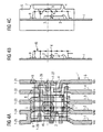
- Figures 4a to 4c show a second embodiment for making a screen cage with an integrated Wire mesh.
- the wire mesh 4 before Insertion in an injection mold and before wrapping with a transparent injection molding compound with the leadframe 1 connected.
- the wire mesh is in turn under Providing a front 45 and several lateral Bent areas.
- Leadframe 1 is the wire mesh open.
- the wire mesh 4 is now at its lateral Areas with each frame 1-21 to 1-27 of the crowd lead 1-2 firmly connected to attachment points 8. For example, a selective soldering is done with the arms of the crowd lead.
- the individual arms 1-21 to 1-27 of the crowd lead have sufficient stability to after Attach the wire mesh not in an undesirable manner deflect.
- the invention is not limited in its design to the embodiments shown above. So is it is obvious to the skilled person that the exact nature and Way of connecting the wire mesh with the leadframe is not essential. It depends only on that one Wire mesh is integrated into the device and thereby together with a leadframe that carries the hiking module, forms an electromagnetic screen cage.
Landscapes
- Shielding Devices Or Components To Electric Or Magnetic Fields (AREA)
- Light Receiving Elements (AREA)
Abstract
Description
mit mindestens einem Masse-Kontakt des Leadframes unter Ausbildung eines Schirmkäfigs, in dem sich das Wandlerbauelement befindet, verbunden.
- Figur 1a
- ein Ausführungsbeispiel einer optoelektronischen Vorrichtung mit einem Sendebauelement und einem Schirmkäfig in Vorderansicht;
- Figur 1b
- ein Ausführungsbeispiel einer optoelektronischen Vorrichtung mit einem Empfangsbauelement und einem Schirmkäfig in Vorderansicht;
- Figur 1c
- eine Seitenansicht einer Vorrichtung gemäß Figur 1a oder Figur 1b;
- Figur 2
- eine teilweise geschnittene Ansicht einer Anordnung mit einem Bodenteil einer Spritzgussvorrichtung und einem in die Spritzgussvorrichtung eingebrachten Leadframe sowie einem auf dem Leadframe angeordenten Laser-Chip;
- Figur 3
- eine teilweise geschnittene Ansicht einer Anordnung mit einem Bodenteil einer Spritzgussvorrichtung und einem in die Spritzgussvorrichtung eingebrachten Leadframe und einem auf dem Leadframe angeordenten Fotodioden-Chip;
- Figur 4a
- ein Leadframe mit darauf angeordneten Komponenten sowie einem Drahtgeflecht;
- Figur 4b
- die Anordnung der Figur 4a in Seitenansicht und
- Figur 4c
- die Anordnung der in Figur 4a in Seitenansicht, wobei das Leadframe und die auf dem Leadframe angeordneten Komponenten mit einem transparenten Vergussmaterial umhüllt sind.
Claims (22)
- Optoelektronische Vorrichtung aufweisend:mindestens ein optoelektronisches Wandlerbauelement (2),ein Leadframe (1), auf dem das Wandlerbauelement (2) angeordnet ist,ein Gehäuse (5), das das Wandlerbauelement (2) zumindest teilweise umgibt, undein Drahtgeflecht (4), wobeidas Drahtgeflecht (4) zumindest teilweise in das Gehäuse (5) eingebettet undmit mindestens einem Masse-Kontakt (1-2; 1-21 bis 1-27) des Leadframes (1) unter Ausbildung eines Schirmkäfigs, in dem sich das Wandlerbauelement (2) befindet, verbunden ist.
- Vorrichtung nach Anspruch 1, wobei das Drahtgeflecht (4) im Bereich des optischen Fensters des Wandlerbauelementes (2) eine Öffnung (41) besitzt.
- Vorrichtung nach Anspruch 2, wobei das Gehäuse (5) im Bereich des optischen Fensters des Wandlerbauelementes (2) eine optische Funktionsfläche (6) aufweist und die Öffnung (41) im Drahtgeflecht (4) im Bereich der optischen Funktionsfläche (6) ausgebildet ist.
- Vorrichtung nach Anspruch 1, wobei das Drahtgeflecht (4) eine zum Leadframe (1) beabstandete Vorderseite (45) und mindestens einen zur Vorderseite (45) im Wesentlichen senkrecht sich in Richtung des Leadframes (1) erstreckenden seitlichen Bereich (42, 43, 44) ausbildet.
- Vorrichtung nach Anspruch 4, wobei das Drahtgeflecht (4) an mindestens einem seitlichen Bereich (42, 43, 44) mit mindestens einem Masse-Kontakt (1-21 bis 1-27) des Leadframes (1) elektrisch verbunden ist.
- Vorrichtung nach Anspruch 4, wobei die Vorderseite (45) des Drahtgeflechts (4) mit einem Masse-Kontakt (1-2) des Leadframes (1) verbunden ist und das Gehäuse (5) hierzu eine Schräge ausbildet.
- Vorrichtung nach Anspruch 1, wobei ein nicht leitender Abstandhalter (9) an der den Kontakt-Pins des Leadframes (1) benachbarten Vorderseite (45) des Drahtgeflechts (4) in dieses integriert ist.
- Vorrichtung nach Anspruch 1, wobei auf dem Leadframe (1) zusätzlich ein dem optoelektronischen Wandlerbauelement (2) zugeordnetes elektrisches Bauelement angeordnet ist.
- Vorrichtung nach Anspruch 1, wobei das Wandlerbauelement (2) auf einem Trägerelement (11) angeordnet und das Trägerelement (11) auf dem Leadframe (1) angeordnet ist.
- Vorrichtung nach Anspruch 1, wobei der Durchmesser des Drahts des Drahtsgeflechts (4) mindestens 30 µm, insbesondere mindestens 50 µm beträgt.
- Vorrichtung nach Anspruch 1, wobei die Maschenweite des Drahtgeflechtes (4) zwischen 50 und 500 µm beträgt.
- Vorrichtung nach Anspruch 1, wobei das Drahtgeflecht (4) aus Kupferdraht oder Aluminiumdraht besteht.
- Vorrichtung nach Anspruch 1, wobei das mindestens eine Wandlerbauelement (2) ein Sendebauelement und/oder ein Empfangsbauelement ist.
- Vorrichtung nach Anspruch 13, wobei die Vorrichtung einen optoelektronischen Transceiver mit einem Sendebauelement und einem Empfangsbauelement bildet.
- Vorrichtung nach Anspruch 1, wobei das Gehäuse (5) ein aus einem Vergussmaterial bestehendes Kunststoffgehäuse ist.
- Verfahren zur Herstellung einer optoelektronischen Vorrichtung mit einem integrierten Schirmkäfig, mit den folgenden Schritten:Anordnen des Wandlerbauelements (2) auf einem Leadframe (1),elektrisches Kontaktieren des Wandlerbauelements (2),Bereitstellen eines Drahtgeflechts (4), das derart gebogen ist, dass es eine an mindestens einer Seite offene Struktur bildet,Verbinden des Drahtgeflecht (4) mit mindestens einem Masse-Lead (1-2; 1-21 bis 1-27) des Leadframes, wobei eine offene Seite der Struktur des Drahtgeflechts (4) unter Ausbildung eines Schirmkäfigs durch das Leadframe (1) geschlossen wird,Einlegen des Leadframes (1) mit nach unten hängendem Drahtgeflecht (4) in eine Gießform, undEinbringen eines Vergussmaterials in die Gießform, wobeidas erhärtete Vergussmaterial ein Gehäuse (5) der optoelektronische Vorrichtung ausbildet unddas Drahtgeflecht (4) in das Gehäuse (5) eingebettet ist.
- Verfahren nach Anspruch 16, wobei in dem Gehäuse (5) bei Einbringen des Vergussmaterials in die Gießform eine optische Funktionsfläche (6) ausgebildet wird.
- Verfahren nach Anspruch 16, wobei das Drahtgeflecht (4) eine Öffnung (41) aufweist und das Drahtgeflecht (4) derart in der Gießform positioniert wird, dass die Öffnung (41) sich im Bereich der zu bildenden optischen Funktionsfläche (6) befindet.
- Verfahren zur Herstellung einer optoelektronischen Vorrichtung mit einem integrierten Schirmkäfig, mit den folgenden Schritten:Anordnen des Wandlerbauelements (2) auf einem Leadframe (1),elektrisches Kontaktieren des Wandlerbauelements (2),Bereitstellen eines eben ausgebreiteten Drahtgeflechts (4),teilweises Einlegen des Drahtgeflechts (4) in die Gießform,Einbringen des Leadframes (1)mit dem Wandlerbauelement (2) in die Gießform beabstandet zu dem Drahtgeflecht (4),Einbringen eines Vergussmaterials in die Gießform, wobei das erhärtete Vergussmaterial ein Gehäuse (5) der optoelektronischen Vorrichtung ausbildet und das Drahtgeflecht (4) teilweise in das Gehäuse (5) eingebettet wird,nach Erhärten des Vergussmaterials Umbiegen seitlich des Gehäuses (5) angeordneter Bereiche des Drahgeflechts (4) in Richtung des Leadframe (1),Verbinden mindestens eines umgebogenen Bereichs des Drahtgeflechts mit mindestens einem Masse-Kontakt (1-2; 1-21 bis 1-27) des Leadframes (1) unter Ausbildung eines Schirmkäfigs.
- Verfahren nach Anspruch 19, wobei in dem Gehäuse (5) bei Einbringen des Vergussmaterials in die Gießform eine optische Funktionsfläche (6) ausgebildet wird.
- Verfahren nach Anspruch 20, wobei das Drahtgeflecht (5) eine Öffnung (41) aufweist und das Drahtgeflecht (4) derart in der Gießform positioniert wird, dass die Öffnung (41) sich im Bereich der zu bildenden optischen Funktionsfläche (6) befindet.
- Verfahren nach Anspruch 19, wobei die Herstellung der Vorrichtung auf einem Multinest-Werkzeug erfolgt, nach dem Gießvorgang die einzelnen Vorrichtungen des Multinest-Werkzeugs vereinzelt werden und hierbei das Drahtgeflecht (4) im Bereich zwischen den einzelnen Vorrichtungen durchtrennt wird, wodurch seitlich des Gehäuses (5) angeordnete Bereiche (42, 43, 44) des Drahtgeflechtes (4) zur Verfügung gestellt werden, die in Richtung des Leadframes (1) biegbar sind.
Applications Claiming Priority (2)
| Application Number | Priority Date | Filing Date | Title |
|---|---|---|---|
| US10/871,315 US20050278936A1 (en) | 2004-06-18 | 2004-06-18 | Optoelectronic apparatus with a shielding cage, and methods for production of an optoelectronic apparatus with a shielding cage. |
| US871315 | 2004-06-18 |
Publications (2)
| Publication Number | Publication Date |
|---|---|
| EP1608026A2 true EP1608026A2 (de) | 2005-12-21 |
| EP1608026A3 EP1608026A3 (de) | 2006-02-08 |
Family
ID=34993367
Family Applications (1)
| Application Number | Title | Priority Date | Filing Date |
|---|---|---|---|
| EP05090173A Withdrawn EP1608026A3 (de) | 2004-06-18 | 2005-06-10 | Optoelektronische Vorrichtung und Verfahren zur Herstellung einer optoelektronischen Vorrichtung |
Country Status (2)
| Country | Link |
|---|---|
| US (1) | US20050278936A1 (de) |
| EP (1) | EP1608026A3 (de) |
Cited By (1)
| Publication number | Priority date | Publication date | Assignee | Title |
|---|---|---|---|---|
| EP2827368A1 (de) * | 2013-07-19 | 2015-01-21 | ams AG | Verpackung für einen optischen Sensor, Anordnung eines optischen Sensor und Verfahren zur Herstellung einer Verpackung für einen optischen Sensor |
Families Citing this family (4)
| Publication number | Priority date | Publication date | Assignee | Title |
|---|---|---|---|---|
| FR2946459B1 (fr) * | 2009-06-05 | 2011-08-05 | Centre Nat Etd Spatiales | Element de structure pour panneau solaire, et structure comportant un tel element |
| US8265487B2 (en) * | 2009-07-29 | 2012-09-11 | Avago Technologies Fiber Ip (Singapore) Pte. Ltd. | Half-duplex, single-fiber (S-F) optical transceiver module and method |
| US8994397B2 (en) * | 2011-11-15 | 2015-03-31 | Texas Instruments Incorporated | Thermal pad shorts test for wire bonded strip testing |
| US10204842B2 (en) * | 2017-02-15 | 2019-02-12 | Texas Instruments Incorporated | Semiconductor package with a wire bond mesh |
Citations (4)
| Publication number | Priority date | Publication date | Assignee | Title |
|---|---|---|---|---|
| US5309321A (en) * | 1992-09-22 | 1994-05-03 | Microelectronics And Computer Technology Corporation | Thermally conductive screen mesh for encapsulated integrated circuit packages |
| JPH07321254A (ja) * | 1994-05-25 | 1995-12-08 | Nec Corp | 樹脂封止型半導体装置およびその製造方法 |
| EP1028339A2 (de) * | 1999-02-09 | 2000-08-16 | Sumitomo Electric Industries, Ltd. | Licht sendendes/empfangendes Modul |
| WO2002017394A1 (en) * | 2000-08-22 | 2002-02-28 | Conexant Systems, Inc. | Molded shield structures and method for their fabrication |
Family Cites Families (4)
| Publication number | Priority date | Publication date | Assignee | Title |
|---|---|---|---|---|
| US5337396A (en) * | 1993-01-22 | 1994-08-09 | Optical Communication Products, Inc. | Conductive plastic optical-electronic interface module |
| DE19947889C2 (de) * | 1999-10-05 | 2003-03-06 | Infineon Technologies Ag | Optoelektronisches, bidirektionales Sende- und Empfangsmodul in Leadframe-Technik |
| EP1160875A1 (de) * | 2000-05-13 | 2001-12-05 | Tyco Electronics AMP GmbH | Elektrooptisches Bauelement mit einem metallbeschichteten Gehäuse |
| US6661677B1 (en) * | 2002-08-12 | 2003-12-09 | Sun Microsystems, Inc. | Disc drive cage |
-
2004
- 2004-06-18 US US10/871,315 patent/US20050278936A1/en not_active Abandoned
-
2005
- 2005-06-10 EP EP05090173A patent/EP1608026A3/de not_active Withdrawn
Patent Citations (4)
| Publication number | Priority date | Publication date | Assignee | Title |
|---|---|---|---|---|
| US5309321A (en) * | 1992-09-22 | 1994-05-03 | Microelectronics And Computer Technology Corporation | Thermally conductive screen mesh for encapsulated integrated circuit packages |
| JPH07321254A (ja) * | 1994-05-25 | 1995-12-08 | Nec Corp | 樹脂封止型半導体装置およびその製造方法 |
| EP1028339A2 (de) * | 1999-02-09 | 2000-08-16 | Sumitomo Electric Industries, Ltd. | Licht sendendes/empfangendes Modul |
| WO2002017394A1 (en) * | 2000-08-22 | 2002-02-28 | Conexant Systems, Inc. | Molded shield structures and method for their fabrication |
Cited By (3)
| Publication number | Priority date | Publication date | Assignee | Title |
|---|---|---|---|---|
| EP2827368A1 (de) * | 2013-07-19 | 2015-01-21 | ams AG | Verpackung für einen optischen Sensor, Anordnung eines optischen Sensor und Verfahren zur Herstellung einer Verpackung für einen optischen Sensor |
| WO2015007485A1 (en) * | 2013-07-19 | 2015-01-22 | Ams Ag | Package for an optical sensor, optical sensor arrangement and method of producing a package for an optical sensor |
| US10396111B2 (en) | 2013-07-19 | 2019-08-27 | Ams Ag | Package for an optical sensor, optical sensor arrangement and method of producing a package for an optical sensor |
Also Published As
| Publication number | Publication date |
|---|---|
| US20050278936A1 (en) | 2005-12-22 |
| EP1608026A3 (de) | 2006-02-08 |
Similar Documents
| Publication | Publication Date | Title |
|---|---|---|
| EP1174745B1 (de) | Optoelektronisches oberflächenmontierbares Modul | |
| DE19829197C2 (de) | Strahlungsaussendendes und/oder -empfangendes Bauelement | |
| DE102008060615B4 (de) | Licht aussendende Diode | |
| DE10243247A1 (de) | Leadframe-basiertes Bauelement-Gehäuse, Leadframe-Band, oberflächenmontierbares elektronisches Bauelement und Verfahren zur Herstellung | |
| EP1252540A2 (de) | Optisches sende-/empfangsmodul mit internem lichtwellenleiter | |
| EP1597764A1 (de) | Optoelektronisches bauteil mit strukturiert metallisiertem gehäusekörper, verfahren zur herstellung eines derartigen bauteils und verfahren zur strukturierten metallisierung eines kunststoff enthaltenden körpers | |
| WO2012155984A1 (de) | Optoelektronische vorrichtung und verfahren zur herstellung von optoelektronischen vorrichtungen | |
| DE10351704B4 (de) | Optoelektronische Sende- und/oder Empfangsanordnung mit einem opto-elektronischen Wandlermodul | |
| DE3244882A1 (de) | Sende- oder empfangsvorrichtung mit einer mittels eines traegers gehalterten diode | |
| DE2922949A1 (de) | Vorrichtung zum anschluss wenigstens einer licht emittierenden diode an einen optischen lichtleiter | |
| DE102017110317A1 (de) | Abdeckung für ein optoelektronisches Bauelement und optoelektronisches Bauteil | |
| EP1168022A2 (de) | Optomodul mit durchkontaktiertem Trägersubstrat | |
| DE69213778T2 (de) | Verfahren zur Herstellung eines opto-elektronischen Bauteils | |
| DE102008003971A1 (de) | Leuchtdiodenanordnung mit Schutzrahmen | |
| EP1608026A2 (de) | Optoelektronische Vorrichtung und Verfahren zur Herstellung einer optoelektronischen Vorrichtung | |
| DE10139166B4 (de) | Oberflächenwellenbauelement | |
| DE102006061722B4 (de) | Anschlussmodul und Verfahren zum Herstellen desselben | |
| DE10227544B4 (de) | Vorrichtung zur optischen Datenübertragung | |
| EP1717871A2 (de) | Oberflächenmontierbares optoelektronisches Bauelement | |
| EP1653265A1 (de) | Anordnung zur optischen Kopplung eines Lichtwellenleiters mit einer optischen Einheit eines optischen Moduls sowie Koppelelement für eine solche Anordnung | |
| EP1591813B1 (de) | Verfahren zur Ausrichtung eines Lichtwellenleiters in Bezug auf eine optische Einheit eines optischen Moduls, optisches Modul und Bausatz mit einem optischen Modul | |
| DE102015102717A1 (de) | Ausgeformte Leiterrahmen für eine Leiterplatte-zu-Leiterplatte-Verbindung | |
| DE102014110719A1 (de) | Halbleiterbauelement, Beleuchtungsvorrichtung und Verfahren zur Herstellung eines Halbleiterbauelements | |
| DE10002328B4 (de) | Optische Sende- und Empfangseinheit mit einer zwei Lichtdurchgangsöffnungen aufweisenden Montageplattform | |
| EP1477833A2 (de) | Optoelektronische Sende- und/oder Empfangsanordnung |
Legal Events
| Date | Code | Title | Description |
|---|---|---|---|
| PUAI | Public reference made under article 153(3) epc to a published international application that has entered the european phase |
Free format text: ORIGINAL CODE: 0009012 |
|
| AK | Designated contracting states |
Kind code of ref document: A2 Designated state(s): AT BE BG CH CY CZ DE DK EE ES FI FR GB GR HU IE IS IT LI LT LU MC NL PL PT RO SE SI SK TR |
|
| AX | Request for extension of the european patent |
Extension state: AL BA HR LV MK YU |
|
| PUAL | Search report despatched |
Free format text: ORIGINAL CODE: 0009013 |
|
| AK | Designated contracting states |
Kind code of ref document: A3 Designated state(s): AT BE BG CH CY CZ DE DK EE ES FI FR GB GR HU IE IS IT LI LT LU MC NL PL PT RO SE SI SK TR |
|
| AX | Request for extension of the european patent |
Extension state: AL BA HR LV MK YU |
|
| 17P | Request for examination filed |
Effective date: 20060117 |
|
| AKX | Designation fees paid |
Designated state(s): DE FR GB |
|
| RAP1 | Party data changed (applicant data changed or rights of an application transferred) |
Owner name: INFINEON TECHNOLOGIES AG |
|
| STAA | Information on the status of an ep patent application or granted ep patent |
Free format text: STATUS: THE APPLICATION IS DEEMED TO BE WITHDRAWN |
|
| 18D | Application deemed to be withdrawn |
Effective date: 20080730 |