EP1608009A1 - Semiconductor device - Google Patents
Semiconductor device Download PDFInfo
- Publication number
- EP1608009A1 EP1608009A1 EP04707668A EP04707668A EP1608009A1 EP 1608009 A1 EP1608009 A1 EP 1608009A1 EP 04707668 A EP04707668 A EP 04707668A EP 04707668 A EP04707668 A EP 04707668A EP 1608009 A1 EP1608009 A1 EP 1608009A1
- Authority
- EP
- European Patent Office
- Prior art keywords
- functional area
- semiconductor device
- functional
- area
- bumps
- Prior art date
- Legal status (The legal status is an assumption and is not a legal conclusion. Google has not performed a legal analysis and makes no representation as to the accuracy of the status listed.)
- Withdrawn
Links
Images


Classifications
-
- H—ELECTRICITY
- H01—ELECTRIC ELEMENTS
- H01L—SEMICONDUCTOR DEVICES NOT COVERED BY CLASS H10
- H01L23/00—Details of semiconductor or other solid state devices
- H01L23/52—Arrangements for conducting electric current within the device in operation from one component to another, i.e. interconnections, e.g. wires, lead frames
-
- H—ELECTRICITY
- H01—ELECTRIC ELEMENTS
- H01L—SEMICONDUCTOR DEVICES NOT COVERED BY CLASS H10
- H01L24/00—Arrangements for connecting or disconnecting semiconductor or solid-state bodies; Methods or apparatus related thereto
- H01L24/80—Methods for connecting semiconductor or other solid state bodies using means for bonding being attached to, or being formed on, the surface to be connected
- H01L24/81—Methods for connecting semiconductor or other solid state bodies using means for bonding being attached to, or being formed on, the surface to be connected using a bump connector
-
- H—ELECTRICITY
- H01—ELECTRIC ELEMENTS
- H01L—SEMICONDUCTOR DEVICES NOT COVERED BY CLASS H10
- H01L23/00—Details of semiconductor or other solid state devices
- H01L23/48—Arrangements for conducting electric current to or from the solid state body in operation, e.g. leads, terminal arrangements ; Selection of materials therefor
- H01L23/50—Arrangements for conducting electric current to or from the solid state body in operation, e.g. leads, terminal arrangements ; Selection of materials therefor for integrated circuit devices, e.g. power bus, number of leads
-
- H—ELECTRICITY
- H01—ELECTRIC ELEMENTS
- H01L—SEMICONDUCTOR DEVICES NOT COVERED BY CLASS H10
- H01L24/00—Arrangements for connecting or disconnecting semiconductor or solid-state bodies; Methods or apparatus related thereto
- H01L24/01—Means for bonding being attached to, or being formed on, the surface to be connected, e.g. chip-to-package, die-attach, "first-level" interconnects; Manufacturing methods related thereto
- H01L24/10—Bump connectors ; Manufacturing methods related thereto
- H01L24/12—Structure, shape, material or disposition of the bump connectors prior to the connecting process
- H01L24/14—Structure, shape, material or disposition of the bump connectors prior to the connecting process of a plurality of bump connectors
-
- H—ELECTRICITY
- H01—ELECTRIC ELEMENTS
- H01L—SEMICONDUCTOR DEVICES NOT COVERED BY CLASS H10
- H01L24/00—Arrangements for connecting or disconnecting semiconductor or solid-state bodies; Methods or apparatus related thereto
- H01L24/01—Means for bonding being attached to, or being formed on, the surface to be connected, e.g. chip-to-package, die-attach, "first-level" interconnects; Manufacturing methods related thereto
- H01L24/10—Bump connectors ; Manufacturing methods related thereto
- H01L24/15—Structure, shape, material or disposition of the bump connectors after the connecting process
- H01L24/17—Structure, shape, material or disposition of the bump connectors after the connecting process of a plurality of bump connectors
-
- H—ELECTRICITY
- H01—ELECTRIC ELEMENTS
- H01L—SEMICONDUCTOR DEVICES NOT COVERED BY CLASS H10
- H01L2224/00—Indexing scheme for arrangements for connecting or disconnecting semiconductor or solid-state bodies and methods related thereto as covered by H01L24/00
- H01L2224/01—Means for bonding being attached to, or being formed on, the surface to be connected, e.g. chip-to-package, die-attach, "first-level" interconnects; Manufacturing methods related thereto
- H01L2224/10—Bump connectors; Manufacturing methods related thereto
- H01L2224/15—Structure, shape, material or disposition of the bump connectors after the connecting process
- H01L2224/16—Structure, shape, material or disposition of the bump connectors after the connecting process of an individual bump connector
- H01L2224/161—Disposition
- H01L2224/16151—Disposition the bump connector connecting between a semiconductor or solid-state body and an item not being a semiconductor or solid-state body, e.g. chip-to-substrate, chip-to-passive
- H01L2224/16221—Disposition the bump connector connecting between a semiconductor or solid-state body and an item not being a semiconductor or solid-state body, e.g. chip-to-substrate, chip-to-passive the body and the item being stacked
- H01L2224/16225—Disposition the bump connector connecting between a semiconductor or solid-state body and an item not being a semiconductor or solid-state body, e.g. chip-to-substrate, chip-to-passive the body and the item being stacked the item being non-metallic, e.g. insulating substrate with or without metallisation
-
- H—ELECTRICITY
- H01—ELECTRIC ELEMENTS
- H01L—SEMICONDUCTOR DEVICES NOT COVERED BY CLASS H10
- H01L2224/00—Indexing scheme for arrangements for connecting or disconnecting semiconductor or solid-state bodies and methods related thereto as covered by H01L24/00
- H01L2224/80—Methods for connecting semiconductor or other solid state bodies using means for bonding being attached to, or being formed on, the surface to be connected
- H01L2224/81—Methods for connecting semiconductor or other solid state bodies using means for bonding being attached to, or being formed on, the surface to be connected using a bump connector
- H01L2224/818—Bonding techniques
- H01L2224/81801—Soldering or alloying
-
- H—ELECTRICITY
- H01—ELECTRIC ELEMENTS
- H01L—SEMICONDUCTOR DEVICES NOT COVERED BY CLASS H10
- H01L2924/00—Indexing scheme for arrangements or methods for connecting or disconnecting semiconductor or solid-state bodies as covered by H01L24/00
- H01L2924/01—Chemical elements
- H01L2924/01005—Boron [B]
-
- H—ELECTRICITY
- H01—ELECTRIC ELEMENTS
- H01L—SEMICONDUCTOR DEVICES NOT COVERED BY CLASS H10
- H01L2924/00—Indexing scheme for arrangements or methods for connecting or disconnecting semiconductor or solid-state bodies as covered by H01L24/00
- H01L2924/01—Chemical elements
- H01L2924/01006—Carbon [C]
-
- H—ELECTRICITY
- H01—ELECTRIC ELEMENTS
- H01L—SEMICONDUCTOR DEVICES NOT COVERED BY CLASS H10
- H01L2924/00—Indexing scheme for arrangements or methods for connecting or disconnecting semiconductor or solid-state bodies as covered by H01L24/00
- H01L2924/01—Chemical elements
- H01L2924/01033—Arsenic [As]
-
- H—ELECTRICITY
- H01—ELECTRIC ELEMENTS
- H01L—SEMICONDUCTOR DEVICES NOT COVERED BY CLASS H10
- H01L2924/00—Indexing scheme for arrangements or methods for connecting or disconnecting semiconductor or solid-state bodies as covered by H01L24/00
- H01L2924/013—Alloys
- H01L2924/014—Solder alloys
-
- H—ELECTRICITY
- H01—ELECTRIC ELEMENTS
- H01L—SEMICONDUCTOR DEVICES NOT COVERED BY CLASS H10
- H01L2924/00—Indexing scheme for arrangements or methods for connecting or disconnecting semiconductor or solid-state bodies as covered by H01L24/00
- H01L2924/30—Technical effects
- H01L2924/301—Electrical effects
- H01L2924/30105—Capacitance
Definitions
- the present invention relates to a semiconductor device including, on a substrate, a first functional area including a storage area and the like, a second functional area including a driving circuit and the like, and an electrode for externally inputting and outputting a signal.
- a method of fixing the chip onto the external substrate through hot pressing using a solder bump is known.
- a bump connection pad is disposed on the DRAM chip, a load is applied to a DRAM cell array at the time of a bump connection (assembling) if the bump connection pad is provided immediately above the DRAM cell array. Therefore, there arises a problem that the DRAM cell array is damaged, the characteristics of the DRAM cell array are degraded, or the like.
- Figs. 8A and 8B are schematic views illustrating a conventional semiconductor device, where Fig. 8A is a plan view and Fig. 8B is a sectional view.
- the semiconductor device has such a structure that a substrate 10 including a DRAM chip and the like is connected to an external substrate 20 including an LSI such as a signal processing chip through bumps B.
- bump connection pads and the bumps B are disposed in a second functional area 2 where the other signal processing circuits and the like are formed, so as to avoid the same surface of a DRAM cell array area (a first functional area 1) formed on the DRAM chip.
- a technique related to the arrangement of a bonding pad for connecting a bonding wire is disclosed in Patent Document 1.
- Patent Document 1 Japanese Patent Application Publication No. Hei 4-162664
- the bump connection pads and the bumps are disposed so as to avoid the DRAM cell array area. Therefore, the DRAM cell array is not affected even if a load is applied through the bumps at the connection of the DRAM chip.
- the bump connection pads and the bumps are disposed so as to be separated from each other, for example, at both ends on the DRAM chip, there arises a problem that a yield at the time of the bump connection (assembling) is lowered. Specifically, even a slight inclination of the DRAM chip causes a variation in load applied to the bumps provided at both horizontal ends. Uniform pressure connection for all the bumps becomes difficult, for example, a bump at one end is successfully connected whereas a bump at the other end is not fully seated, resulting in lowered reliability of products.
- a semiconductor device including a first functional area and a second functional area, which are provided on a substrate, wherein an electrode for externally inputting and outputting a signal is provided so as to overlap the second functional area provided inside a circumscribed rectangle of the first functional area when the substrate is viewed in a planar fashion.
- the electrodes are provided so as to overlap the second functional area provided inside the circumscribed rectangle of the first functional area. Therefore, the electrodes are collectively arranged in approximately the center of the substrate. As a result, a pressure can be prevented from being applied to the first functional area upon connection. At the same time, pressure connection to an external substrate through the electrodes can be achieved without expanding the area where the electrodes are arranged. Thus, uniform connection to the electrodes can be achieved.
- Figs. 1A and 1B are schematic views for illustrating a semiconductor device according to a first embodiment, where Fig. 1A is a plan view and Fig. 1B is a sectional view.
- the semiconductor device includes first functional areas 1 and a second functional area 2 provided on a chip-like substrate 10.
- the first functional area 1 serves as a DRAM cell array (a storage element area), whereas the second functional area 2 serves as a signal processing circuit or a driving circuit for the DRAM cell array .
- the semiconductor device according to the first embodiment has two first functional areas (1a and 1b).
- Bumps (metal projections) B for externally inputting and outputting a signal are provided in the second functional area 2, which is an area between the first functional areas (an inner area of a circumscribed rectangle when the first functional areas 1 are viewed in a planar fashion).
- the semiconductor device is connected face-down to an external substrate 20 through the bumps B.
- the bumps B can be provided in approximately the center of the substrate 10 so as not to be situated directly above the DRAM cell arrays corresponding to the first functional areas 1. Therefore, at heat pressure connection of the semiconductor device to the external substrate 20 through the bumps B, a pressure is not applied from the bumps B to the DRAM cell arrays (the first functional areas 1).
- the DRAM cell arrays corresponding to the first functional areas 1 have lower resistance against the applied pressure per given area (hereinafter, referred to simply as "resistance against the applied pressure") than that of the area of the signal processing circuit or the driving circuit corresponding to the second functional area 2. Therefore, a pressure is not applied from the bumps B to the DRAM cell arrays (the first functional areas 1), thereby making possible to prevent the DRAM cell arrays from being damaged.
- the bumps B are disposed in approximately the center of the substrate 10, a distance between the bumps at both extremities can be reduced as compared with the case where the bumps are provided at the ends of the substrate 10, and even if the substrate 10 is inclined to some degree, uniform bump connection to the external substrate 20 can be achieved.
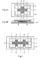
- Figs. 2A and 2B are schematic views for illustrating a semiconductor device according to a second embodiment, where Fig. 2A is a plan view and Fig. 2B is a sectional view.
- the semiconductor device includes the first functional areas 1 and the second functional area 2 provided on the chip-like substrate 10.
- the plurality of bumps B are provided in a cross-like pattern in the second functional area 2, which is an area between the first functional areas (an inner area of a circumscribed rectangle when the first functional areas 1 are viewed in a planar fashion).
- the semiconductor device is connected face-down to the external substrate 20 through the bumps B.
- the bumps B can be provided in approximately the center of the substrate 10 so as not to be situated directly above the DRAM cell arrays corresponding to the first functional areas 1. Therefore, at heat pressure connection of the semiconductor device to the external substrate 20 through the bumps B, the same functional effects as those in the previously described example are obtained. Specifically, a pressure is not applied from the bumps B to the DRAM cell arrays (the first functional areas 1) which have lower resistance against the applied pressure (lower resistance against the applied pressure than that of the area of the signal processing circuit or the driving circuit corresponding to the second functional area 2). Therefore, the DRAM cell arrays can be prevented from being damaged.
- the plurality of bumps B are arranged in a cross-like pattern.
- the bumps can be arranged in approximately the center of the substrate 10.
- a wiring distance between each of the bumps B and the first functional area 1 can be reduced as much as possible, so that a signal delay can be prevented.
- Fig. 3 is a schematic plan view for illustrating a semiconductor device according to a third embodiment.
- the semiconductor device is an example of application of the semiconductor device shown in Figs. 2A and 2B according to the second embodiment, and includes the first functional areas 1 and the second functional area 2 provided on the chip-like substrate 10.
- the plurality of bumps B are provided in a contiguous cross-like pattern in the second functional area 2, which is an area between the first functional areas 1 (an inner area of a circumscribed rectangle when the first functional areas 1 are viewed in a planar fashion).
- any number of the first functional areas 1 may be provided.
- the bumps B are provided at the position in the second functional area 2, which is an area between the first functional areas (for example, 1a to 1f).
- the arrangement of the bumps in approximately the center of the substrate 10 and the reduction of the wiring distance between each of the bumps B and the first functional areas 1 can be achieved at the same time.
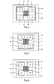
- Fig. 4 is a schematic plan view for illustrating a semiconductor device according to a fourth embodiment.
- the semiconductor device is an example of application of the semiconductor device shown in Fig. 2 according to the second embodiment, and includes the first functional areas 1 and the second functional area 2 provided on the chip-like substrate 10.
- the plurality of bumps B are provided in a rectangular pattern in the second functional area 2, which is an area between the first functional areas (an inner area of a circumscribed rectangle when the first functional areas 1 are viewed in a planar fashion).
- the bumps can be arranged in approximately the center of the substrate 10 while the reduction of the wiring distance between each of the bumps B and the first functional areas 1 can be made possible.
- Fig. 5 is a schematic plan view for illustrating a semiconductor device according to a fifth embodiment.
- the semiconductor device is an example of application of the semiconductor device shown in Fig. 4 according to the fourth embodiment, and includes the first functional areas 1 and the second functional area 2 provided on the chip-like substrate 10.
- the plurality of bumps B are provided in a rectangular pattern in the second functional area 2, which is an area between the first functional areas (an inner area of a circumscribed rectangle when the first functional areas 1 are viewed in a planar fashion).
- the first functional areas 1 (1a to 1d), each being cut, are arranged so as to surround the bumps B arranged in approximately the center of the substrate 10 in a rectangular pattern.
- the bumps can be arranged in approximately the center of the substrate 10 while the reduction of the wiring distance between each of the bumps B and the first functional areas 1 can be made possible.
- layout efficiency of the substrate 10 can be enhanced.
- Fig. 6 is a schematic plan view for illustrating a semiconductor device according to a sixth embodiment.
- the semiconductor device is an example of application of the semiconductor device shown in Fig. 5 according to the fifth embodiment, and includes the first functional areas 1 and the second functional area 2 provided on the chip-like substrate 10.
- the plurality of bumps B are provided in a rectangular pattern in the second functional area 2, which is an area between the first functional areas (an inner area of a circumscribed rectangle when the first functional areas 1 are viewed in a planar fashion).
- This embodiment particularly differs from the other embodiments in that the corners of the bumps B partially overlap the first functional areas 1. Specifically, it is apparent that an overlap part of the first functional areas 1 with the bumps B is subjected to a pressure upon connection. Therefore, from the very beginning of design, a part of the first functional areas 1, which is pressurized by the bumps B, is set as an invalid area (a non-functioning area) in advance. As a result, the area of the bumps B and the first functional areas 1 can come closer to each other. Therefore, in addition to the effects of the semiconductor device according the fifth embodiment, layout efficiency can also be enhanced.
- Fig. 7 is a schematic plan view for illustrating a semiconductor device according to a seventh embodiment.
- the semiconductor device is arranged so that the second functional area 2 is surrounded by the first functional area 1.
- the bumps B are arranged in the second functional area 2 surrounded by the first functional area 1.
- the first functional area 1 has a continuous annular pattern.
- the second functional area 2 and the bumps B are arranged.
- the bumps B can be arranged in approximately the center of the substrate 10. Moreover, the wiring distance between each of the bumps B and the first functional area 1 can be reduced.
- the plurality of first functional areas 1 may be obtained by dividing a single functional area to be arranged or arranging a plurality of functional areas.
- the DRAM cell array may be divided into a plurality of DRAM cell arrays to be arranged so as to achieve 256 Mbit in total (in this case, a single DRAM cell array obtained by the division corresponds to one first functional area 1).
- a plurality of DRAM cell arrays each being a 256-Mbit DRAM cell array serving as a single first functional area 1, may be arranged (in this case, a total capacity is obtained by: the number of first functional areas 1 ⁇ 256 Mbit).
- the first functional area may include a curve area such as a circle. Furthermore, the same effects can be achieved if an electrode other than the bump B is used as long as it allows connection by the heat pressure.
- the semiconductor device is to be connected to the external substrate by the heat pressure, a pressure through the electrodes is no longer applied to the first functional area, so that and the first functional area is prevented from being damaged. Furthermore, since the arrangement of the electrodes concentrates in approximately the center of the substrate, uniform connection to the electrodes provides a highly reliable apparatus.
Abstract
Description
- The present invention relates to a semiconductor device including, on a substrate, a first functional area including a storage area and the like, a second functional area including a driving circuit and the like, and an electrode for externally inputting and outputting a signal.
- As a technique of connecting a chip (a DRAM chip), on which a memory such as a DRAM (Dynamic Random Access Memory), a driving circuit and the like are formed, to an external substrate, a method of fixing the chip onto the external substrate through hot pressing using a solder bump is known. In the case where a bump connection pad is disposed on the DRAM chip, a load is applied to a DRAM cell array at the time of a bump connection (assembling) if the bump connection pad is provided immediately above the DRAM cell array. Therefore, there arises a problem that the DRAM cell array is damaged, the characteristics of the DRAM cell array are degraded, or the like.
- Therefore, the bump connection pad is conventionally disposed at the position of a peripheral circuit (the driving circuit or the like) so as not to be situated immediately above the DRAM cell array. Figs. 8A and 8B are schematic views illustrating a conventional semiconductor device, where Fig. 8A is a plan view and Fig. 8B is a sectional view. Specifically, the semiconductor device has such a structure that a
substrate 10 including a DRAM chip and the like is connected to anexternal substrate 20 including an LSI such as a signal processing chip through bumps B. In this case, bump connection pads and the bumps B are disposed in a secondfunctional area 2 where the other signal processing circuits and the like are formed, so as to avoid the same surface of a DRAM cell array area (a first functional area 1) formed on the DRAM chip. Moreover, a technique related to the arrangement of a bonding pad for connecting a bonding wire is disclosed inPatent Document 1. - Patent Document 1: Japanese Patent Application Publication No. Hei 4-162664
- In the conventional semiconductor device, the bump connection pads and the bumps are disposed so as to avoid the DRAM cell array area. Therefore, the DRAM cell array is not affected even if a load is applied through the bumps at the connection of the DRAM chip. However, since the bump connection pads and the bumps are disposed so as to be separated from each other, for example, at both ends on the DRAM chip, there arises a problem that a yield at the time of the bump connection (assembling) is lowered. Specifically, even a slight inclination of the DRAM chip causes a variation in load applied to the bumps provided at both horizontal ends. Uniform pressure connection for all the bumps becomes difficult, for example, a bump at one end is successfully connected whereas a bump at the other end is not fully seated, resulting in lowered reliability of products.
- The present invention is devised to solve the above problems. Specifically, in the present invention, a semiconductor device including a first functional area and a second functional area, which are provided on a substrate, wherein an electrode for externally inputting and outputting a signal is provided so as to overlap the second functional area provided inside a circumscribed rectangle of the first functional area when the substrate is viewed in a planar fashion.
- In the present invention described above, the electrodes are provided so as to overlap the second functional area provided inside the circumscribed rectangle of the first functional area. Therefore, the electrodes are collectively arranged in approximately the center of the substrate. As a result, a pressure can be prevented from being applied to the first functional area upon connection. At the same time, pressure connection to an external substrate through the electrodes can be achieved without expanding the area where the electrodes are arranged. Thus, uniform connection to the electrodes can be achieved.
-
- Figs. 1A and 1B are schematic views for illustrating a semiconductor device according to a first embodiment;
- Figs. 2A and 2B are schematic views for illustrating a semiconductor device according to a second embodiment;
- Fig. 3 is a schematic plan view for illustrating a semiconductor device according to a third embodiment;
- Fig. 4 is a schematic plan view for illustrating a semiconductor device according to a fourth embodiment;
- Fig. 5 is a schematic plan view for illustrating a semiconductor device according to a fifth embodiment;
- Fig. 6 is a schematic plan view for illustrating a semiconductor device according to a sixth embodiment;
- Fig. 7 is a schematic plan view for illustrating a semiconductor device according to a seventh embodiment; and
- Figs. 8A and 8B are schematic views for illustrating a conventional semiconductor device.
-
- Hereinafter, embodiments of the present invention will be described based on the drawings. Figs. 1A and 1B are schematic views for illustrating a semiconductor device according to a first embodiment, where Fig. 1A is a plan view and Fig. 1B is a sectional view. Specifically, the semiconductor device includes first
functional areas 1 and a secondfunctional area 2 provided on a chip-like substrate 10. The firstfunctional area 1 serves as a DRAM cell array (a storage element area), whereas the secondfunctional area 2 serves as a signal processing circuit or a driving circuit for the DRAM cell array . - The semiconductor device according to the first embodiment has two first functional areas (1a and 1b). Bumps (metal projections) B for externally inputting and outputting a signal are provided in the second
functional area 2, which is an area between the first functional areas (an inner area of a circumscribed rectangle when the firstfunctional areas 1 are viewed in a planar fashion). The semiconductor device is connected face-down to anexternal substrate 20 through the bumps B. - By the above-mentioned arrangement of each of the components, the bumps B can be provided in approximately the center of the
substrate 10 so as not to be situated directly above the DRAM cell arrays corresponding to the firstfunctional areas 1. Therefore, at heat pressure connection of the semiconductor device to theexternal substrate 20 through the bumps B, a pressure is not applied from the bumps B to the DRAM cell arrays (the first functional areas 1). - Specifically, the DRAM cell arrays corresponding to the first
functional areas 1 have lower resistance against the applied pressure per given area (hereinafter, referred to simply as "resistance against the applied pressure") than that of the area of the signal processing circuit or the driving circuit corresponding to the secondfunctional area 2. Therefore, a pressure is not applied from the bumps B to the DRAM cell arrays (the first functional areas 1), thereby making possible to prevent the DRAM cell arrays from being damaged. - Moreover, since the bumps B are disposed in approximately the center of the
substrate 10, a distance between the bumps at both extremities can be reduced as compared with the case where the bumps are provided at the ends of thesubstrate 10, and even if thesubstrate 10 is inclined to some degree, uniform bump connection to theexternal substrate 20 can be achieved. - Figs. 2A and 2B are schematic views for illustrating a semiconductor device according to a second embodiment, where Fig. 2A is a plan view and Fig. 2B is a sectional view. Specifically, the semiconductor device includes the first
functional areas 1 and the secondfunctional area 2 provided on the chip-like substrate 10. As the firstfunctional areas 1, four functional areas 1 (1a, 1b, 1c and 1d) are provided. The plurality of bumps B are provided in a cross-like pattern in the secondfunctional area 2, which is an area between the first functional areas (an inner area of a circumscribed rectangle when the firstfunctional areas 1 are viewed in a planar fashion). The semiconductor device is connected face-down to theexternal substrate 20 through the bumps B. - By the above-mentioned arrangement of each of the components, the bumps B can be provided in approximately the center of the
substrate 10 so as not to be situated directly above the DRAM cell arrays corresponding to the firstfunctional areas 1. Therefore, at heat pressure connection of the semiconductor device to theexternal substrate 20 through the bumps B, the same functional effects as those in the previously described example are obtained. Specifically, a pressure is not applied from the bumps B to the DRAM cell arrays (the first functional areas 1) which have lower resistance against the applied pressure (lower resistance against the applied pressure than that of the area of the signal processing circuit or the driving circuit corresponding to the second functional area 2). Therefore, the DRAM cell arrays can be prevented from being damaged. - Moreover, the plurality of bumps B are arranged in a cross-like pattern. As a result, the bumps can be arranged in approximately the center of the
substrate 10. At the same time, a wiring distance between each of the bumps B and the firstfunctional area 1 can be reduced as much as possible, so that a signal delay can be prevented. - Fig. 3 is a schematic plan view for illustrating a semiconductor device according to a third embodiment. The semiconductor device is an example of application of the semiconductor device shown in Figs. 2A and 2B according to the second embodiment, and includes the first
functional areas 1 and the secondfunctional area 2 provided on the chip-like substrate 10. As the firstfunctional areas 1, six functional areas 1 (1a, 1b, 1c, 1d, 1e and 1f) are provided. The plurality of bumps B are provided in a contiguous cross-like pattern in the secondfunctional area 2, which is an area between the first functional areas 1 (an inner area of a circumscribed rectangle when the firstfunctional areas 1 are viewed in a planar fashion). - As described above, any number of the first
functional areas 1 may be provided. The bumps B are provided at the position in the secondfunctional area 2, which is an area between the first functional areas (for example, 1a to 1f). As a result, the arrangement of the bumps in approximately the center of thesubstrate 10 and the reduction of the wiring distance between each of the bumps B and the firstfunctional areas 1 can be achieved at the same time. - Fig. 4 is a schematic plan view for illustrating a semiconductor device according to a fourth embodiment. The semiconductor device is an example of application of the semiconductor device shown in Fig. 2 according to the second embodiment, and includes the first
functional areas 1 and the secondfunctional area 2 provided on the chip-like substrate 10. As the firstfunctional areas 1, four functional areas 1 (1a, 1b, 1c and 1d) are provided. The plurality of bumps B are provided in a rectangular pattern in the secondfunctional area 2, which is an area between the first functional areas (an inner area of a circumscribed rectangle when the firstfunctional areas 1 are viewed in a planar fashion). - As a result of the arrangement of each of the components as described above, the bumps can be arranged in approximately the center of the
substrate 10 while the reduction of the wiring distance between each of the bumps B and the firstfunctional areas 1 can be made possible. - Fig. 5 is a schematic plan view for illustrating a semiconductor device according to a fifth embodiment. The semiconductor device is an example of application of the semiconductor device shown in Fig. 4 according to the fourth embodiment, and includes the first
functional areas 1 and the secondfunctional area 2 provided on the chip-like substrate 10. As the firstfunctional areas 1, four functional areas 1 (1a, 1b, 1c and 1d) are provided. The plurality of bumps B are provided in a rectangular pattern in the secondfunctional area 2, which is an area between the first functional areas (an inner area of a circumscribed rectangle when the firstfunctional areas 1 are viewed in a planar fashion). - In this embodiment, the first functional areas 1 (1a to 1d), each being cut, are arranged so as to surround the bumps B arranged in approximately the center of the
substrate 10 in a rectangular pattern. As a result of such arrangement, the bumps can be arranged in approximately the center of thesubstrate 10 while the reduction of the wiring distance between each of the bumps B and the firstfunctional areas 1 can be made possible. At the same time, layout efficiency of thesubstrate 10 can be enhanced. - Fig. 6 is a schematic plan view for illustrating a semiconductor device according to a sixth embodiment. The semiconductor device is an example of application of the semiconductor device shown in Fig. 5 according to the fifth embodiment, and includes the first
functional areas 1 and the secondfunctional area 2 provided on the chip-like substrate 10. As the firstfunctional areas 1, four functional areas 1 (1a, 1b, 1c and 1d) are provided. The plurality of bumps B are provided in a rectangular pattern in the secondfunctional area 2, which is an area between the first functional areas (an inner area of a circumscribed rectangle when the firstfunctional areas 1 are viewed in a planar fashion). - This embodiment particularly differs from the other embodiments in that the corners of the bumps B partially overlap the first
functional areas 1. Specifically, it is apparent that an overlap part of the firstfunctional areas 1 with the bumps B is subjected to a pressure upon connection. Therefore, from the very beginning of design, a part of the firstfunctional areas 1, which is pressurized by the bumps B, is set as an invalid area (a non-functioning area) in advance. As a result, the area of the bumps B and the firstfunctional areas 1 can come closer to each other. Therefore, in addition to the effects of the semiconductor device according the fifth embodiment, layout efficiency can also be enhanced. - Fig. 7 is a schematic plan view for illustrating a semiconductor device according to a seventh embodiment. The semiconductor device is arranged so that the second
functional area 2 is surrounded by the firstfunctional area 1. The bumps B are arranged in the secondfunctional area 2 surrounded by the firstfunctional area 1. Specifically, the firstfunctional area 1 has a continuous annular pattern. In a space in the middle of the first functional area, the secondfunctional area 2 and the bumps B are arranged. - Even if the first
functional area 1 is annular without being divided as described above, the bumps B can be arranged in approximately the center of thesubstrate 10. Moreover, the wiring distance between each of the bumps B and the firstfunctional area 1 can be reduced. - It should be noted that, in each of the embodiments described above, the plurality of first
functional areas 1 may be obtained by dividing a single functional area to be arranged or arranging a plurality of functional areas. For example, if the firstfunctional area 1 is composed of a DRAM cell array, the DRAM cell array may be divided into a plurality of DRAM cell arrays to be arranged so as to achieve 256 Mbit in total (in this case, a single DRAM cell array obtained by the division corresponds to one first functional area 1). Alternatively, a plurality of DRAM cell arrays, each being a 256-Mbit DRAM cell array serving as a single firstfunctional area 1, may be arranged (in this case, a total capacity is obtained by: the number of firstfunctional areas 1 × 256 Mbit). - Although a rectangle shape has been mainly described as the shape of the first
functional area 1, it is not limited thereto. The first functional area may include a curve area such as a circle. Furthermore, the same effects can be achieved if an electrode other than the bump B is used as long as it allows connection by the heat pressure. - As described above, according to the present invention, the following effects are obtained. Specifically, if the semiconductor device is to be connected to the external substrate by the heat pressure, a pressure through the electrodes is no longer applied to the first functional area, so that and the first functional area is prevented from being damaged. Furthermore, since the arrangement of the electrodes concentrates in approximately the center of the substrate, uniform connection to the electrodes provides a highly reliable apparatus.
Claims (7)
- A semiconductor device having, on a substrate, a first functional area and a second functional area, characterized in that:if the substrate is viewed in a planar fashion, an electrode for externally inputting and outputting a signal is provided in the second functional area disposed inside a circumscribed rectangle of the first functional area.
- The semiconductor device according to claim 1, characterized in that:resistance against an applied pressure of the second functional area is larger than resistance against an applied pressure of the first functional area.
- The semiconductor device according to claim 1, characterized in that:the electrode has a bump.
- The semiconductor device according to claim 1, characterized in that:the first functional area has a storage element, and the second functional area has a signal processing circuit or a driving circuit.
- The semiconductor device according to claim 1, characterized in that:the plurality of first functional areas are exist, and the electrodes are disposed between each of the first functional areas.
- The semiconductor device according to claim 5, characterized in that:twoormore first functional areas are exist in lengthwise and crosswise directions.
- The semiconductor device according to claim 1, characterized in that:the second functional area is disposed in a state of being surrounded by the first functional area, and the electrode is disposed in the second functional area surrounded by the first functional area.
Applications Claiming Priority (3)
| Application Number | Priority Date | Filing Date | Title |
|---|---|---|---|
| JP2003040730A JP2004265940A (en) | 2003-02-19 | 2003-02-19 | Semiconductor device |
| JP2003040730 | 2003-02-19 | ||
| PCT/JP2004/001079 WO2004075280A1 (en) | 2003-02-19 | 2004-02-03 | Semiconductor device |
Publications (2)
| Publication Number | Publication Date |
|---|---|
| EP1608009A1 true EP1608009A1 (en) | 2005-12-21 |
| EP1608009A4 EP1608009A4 (en) | 2010-05-19 |
Family
ID=32905262
Family Applications (1)
| Application Number | Title | Priority Date | Filing Date |
|---|---|---|---|
| EP04707668A Withdrawn EP1608009A4 (en) | 2003-02-19 | 2004-02-03 | Semiconductor device |
Country Status (6)
| Country | Link |
|---|---|
| US (1) | US20060186403A1 (en) |
| EP (1) | EP1608009A4 (en) |
| JP (1) | JP2004265940A (en) |
| KR (1) | KR20050100663A (en) |
| TW (1) | TWI246132B (en) |
| WO (1) | WO2004075280A1 (en) |
Cited By (1)
| Publication number | Priority date | Publication date | Assignee | Title |
|---|---|---|---|---|
| EP2249381A1 (en) * | 2008-02-19 | 2010-11-10 | Liquid Design Systems, Inc. | Semiconductor chip and semiconductor device |
Families Citing this family (2)
| Publication number | Priority date | Publication date | Assignee | Title |
|---|---|---|---|---|
| JP2009295740A (en) * | 2008-06-04 | 2009-12-17 | Elpida Memory Inc | Memory chip and semiconductor device |
| JP6963448B2 (en) * | 2017-09-13 | 2021-11-10 | 太陽誘電株式会社 | Electronic components |
Citations (8)
| Publication number | Priority date | Publication date | Assignee | Title |
|---|---|---|---|---|
| EP0220444A2 (en) * | 1985-10-21 | 1987-05-06 | International Business Machines Corporation | Logic-circuit layout for large-scale integrated circuits |
| JPH05343634A (en) * | 1992-06-06 | 1993-12-24 | Hitachi Ltd | Semiconductor storage device |
| US5319224A (en) * | 1989-10-11 | 1994-06-07 | Mitsubishi Denki Kabushiki Kaisha | Integrated circuit device having a geometry to enhance fabrication and testing and manufacturing method thereof |
| US6150728A (en) * | 1995-05-12 | 2000-11-21 | Mitsubishi Denki Kabushiki Kaisha | Semiconductor memory device having a pad arrangement with reduced occupying area |
| US6246121B1 (en) * | 1999-04-12 | 2001-06-12 | Vlsi Technology, Inc. | High performance flip-chip semiconductor device |
| US20010045583A1 (en) * | 1998-01-28 | 2001-11-29 | Fukashi Morishita | Semiconductor memory device capable of performing stable operation for noise while preventing increase in chip area |
| JP2002217298A (en) * | 2001-01-19 | 2002-08-02 | Nec Kansai Ltd | Semiconductor wafer |
| US20020192866A1 (en) * | 1999-02-03 | 2002-12-19 | Rohm Co., Ltd. | Semiconductor device and semiconductor chip for use therein |
Family Cites Families (5)
| Publication number | Priority date | Publication date | Assignee | Title |
|---|---|---|---|---|
| JPH0752762B2 (en) * | 1985-01-07 | 1995-06-05 | 株式会社日立製作所 | Semiconductor resin package |
| JP3383081B2 (en) * | 1994-07-12 | 2003-03-04 | 三菱電機株式会社 | Electronic component manufactured using anodic bonding and method of manufacturing electronic component |
| JPH0888253A (en) * | 1994-09-16 | 1996-04-02 | Nippon Steel Corp | Semiconductor device terminal contacting device |
| US5842628A (en) * | 1995-04-10 | 1998-12-01 | Fujitsu Limited | Wire bonding method, semiconductor device, capillary for wire bonding and ball bump forming method |
| CN1383197A (en) * | 2001-04-25 | 2002-12-04 | 松下电器产业株式会社 | Mfg. method of semiconductor device and semiconductor device |
-
2003
- 2003-02-19 JP JP2003040730A patent/JP2004265940A/en active Pending
-
2004
- 2004-02-03 WO PCT/JP2004/001079 patent/WO2004075280A1/en active Search and Examination
- 2004-02-03 KR KR1020057014633A patent/KR20050100663A/en not_active Application Discontinuation
- 2004-02-03 US US10/543,592 patent/US20060186403A1/en not_active Abandoned
- 2004-02-03 EP EP04707668A patent/EP1608009A4/en not_active Withdrawn
- 2004-02-16 TW TW093103631A patent/TWI246132B/en not_active IP Right Cessation
Patent Citations (8)
| Publication number | Priority date | Publication date | Assignee | Title |
|---|---|---|---|---|
| EP0220444A2 (en) * | 1985-10-21 | 1987-05-06 | International Business Machines Corporation | Logic-circuit layout for large-scale integrated circuits |
| US5319224A (en) * | 1989-10-11 | 1994-06-07 | Mitsubishi Denki Kabushiki Kaisha | Integrated circuit device having a geometry to enhance fabrication and testing and manufacturing method thereof |
| JPH05343634A (en) * | 1992-06-06 | 1993-12-24 | Hitachi Ltd | Semiconductor storage device |
| US6150728A (en) * | 1995-05-12 | 2000-11-21 | Mitsubishi Denki Kabushiki Kaisha | Semiconductor memory device having a pad arrangement with reduced occupying area |
| US20010045583A1 (en) * | 1998-01-28 | 2001-11-29 | Fukashi Morishita | Semiconductor memory device capable of performing stable operation for noise while preventing increase in chip area |
| US20020192866A1 (en) * | 1999-02-03 | 2002-12-19 | Rohm Co., Ltd. | Semiconductor device and semiconductor chip for use therein |
| US6246121B1 (en) * | 1999-04-12 | 2001-06-12 | Vlsi Technology, Inc. | High performance flip-chip semiconductor device |
| JP2002217298A (en) * | 2001-01-19 | 2002-08-02 | Nec Kansai Ltd | Semiconductor wafer |
Non-Patent Citations (1)
| Title |
|---|
| See also references of WO2004075280A1 * |
Cited By (2)
| Publication number | Priority date | Publication date | Assignee | Title |
|---|---|---|---|---|
| EP2249381A1 (en) * | 2008-02-19 | 2010-11-10 | Liquid Design Systems, Inc. | Semiconductor chip and semiconductor device |
| EP2249381A4 (en) * | 2008-02-19 | 2012-11-21 | Liquid Design Systems Inc | Semiconductor chip and semiconductor device |
Also Published As
| Publication number | Publication date |
|---|---|
| EP1608009A4 (en) | 2010-05-19 |
| US20060186403A1 (en) | 2006-08-24 |
| TWI246132B (en) | 2005-12-21 |
| TW200428541A (en) | 2004-12-16 |
| JP2004265940A (en) | 2004-09-24 |
| WO2004075280A1 (en) | 2004-09-02 |
| KR20050100663A (en) | 2005-10-19 |
Similar Documents
| Publication | Publication Date | Title |
|---|---|---|
| US6242814B1 (en) | Universal I/O pad structure for in-line or staggered wire bonding or arrayed flip-chip assembly | |
| JP4731883B2 (en) | Double stacked BGA package and multiple stacked BGA package | |
| US6118180A (en) | Semiconductor die metal layout for flip chip packaging | |
| US6858938B2 (en) | Semiconductor device | |
| US8680691B2 (en) | Semiconductor device having semiconductor member and mounting member | |
| US6836007B2 (en) | Semiconductor package including stacked semiconductor chips | |
| US20020056899A1 (en) | Semiconductor chip and semiconductor device having a chip-on-chip structure | |
| JP2002033441A (en) | Semiconductor device | |
| KR20090034180A (en) | Semiconductor package having interposer and electronic apparatus and method for manufacturing semiconductor package | |
| US7884473B2 (en) | Method and structure for increased wire bond density in packages for semiconductor chips | |
| US6677219B2 (en) | Method of forming a ball grid array package | |
| US7105933B2 (en) | Semiconductor integrated circuit device and manufacturing method of the same | |
| EP1608009A1 (en) | Semiconductor device | |
| JPH10189653A (en) | Semiconductor element and circuit module having this semiconductor element | |
| US6743979B1 (en) | Bonding pad isolation | |
| JPH05243482A (en) | Semiconductor integrated circuit | |
| KR100475740B1 (en) | semiconductor intergrated circuit having pads layout for improving signal integrity and for reducing chip size | |
| US7999370B2 (en) | Semiconductor chip capable of increased number of pads in limited region and semiconductor package using the same | |
| JP4618275B2 (en) | Semiconductor device | |
| JP2004111543A (en) | Semiconductor chip | |
| US20050082580A1 (en) | Structure of wafer level package with area bump | |
| JP2004079559A (en) | Semiconductor chip | |
| JP3574004B2 (en) | Semiconductor device | |
| JP2000349195A (en) | Chip-size package of semiconductor device | |
| JPH08148641A (en) | Layout method and wire bonding method for semiconductor chip |
Legal Events
| Date | Code | Title | Description |
|---|---|---|---|
| PUAI | Public reference made under article 153(3) epc to a published international application that has entered the european phase |
Free format text: ORIGINAL CODE: 0009012 |
|
| 17P | Request for examination filed |
Effective date: 20050811 |
|
| AK | Designated contracting states |
Kind code of ref document: A1 Designated state(s): AT BE BG CH CY CZ DE DK EE ES FI FR GB GR HU IE IT LI LU MC NL PT RO SE SI SK TR |
|
| AX | Request for extension of the european patent |
Extension state: AL LT LV MK |
|
| RIN1 | Information on inventor provided before grant (corrected) |
Inventor name: EZAKI, TAKAYUKI |
|
| RIN1 | Information on inventor provided before grant (corrected) |
Inventor name: EZAKI, TAKAYUKI |
|
| DAX | Request for extension of the european patent (deleted) | ||
| RBV | Designated contracting states (corrected) |
Designated state(s): DE FR GB |
|
| A4 | Supplementary search report drawn up and despatched |
Effective date: 20100416 |
|
| RIC1 | Information provided on ipc code assigned before grant |
Ipc: H01L 27/10 20060101ALN20100412BHEP Ipc: H01L 27/04 20060101ALN20100412BHEP Ipc: H01L 21/82 20060101ALN20100412BHEP Ipc: H01L 21/60 20060101AFI20040906BHEP |
|
| STAA | Information on the status of an ep patent application or granted ep patent |
Free format text: STATUS: THE APPLICATION IS DEEMED TO BE WITHDRAWN |
|
| 18D | Application deemed to be withdrawn |
Effective date: 20100821 |