EP1603164A2 - Memory device and its manufacturing method - Google Patents
Memory device and its manufacturing method Download PDFInfo
- Publication number
- EP1603164A2 EP1603164A2 EP05011305A EP05011305A EP1603164A2 EP 1603164 A2 EP1603164 A2 EP 1603164A2 EP 05011305 A EP05011305 A EP 05011305A EP 05011305 A EP05011305 A EP 05011305A EP 1603164 A2 EP1603164 A2 EP 1603164A2
- Authority
- EP
- European Patent Office
- Prior art keywords
- ferroelectric
- dielectric layer
- ferroelectric capacitor
- substrate
- simple matrix
- Prior art date
- Legal status (The legal status is an assumption and is not a legal conclusion. Google has not performed a legal analysis and makes no representation as to the accuracy of the status listed.)
- Withdrawn
Links
Images








Classifications
-
- G—PHYSICS
- G11—INFORMATION STORAGE
- G11C—STATIC STORES
- G11C11/00—Digital stores characterised by the use of particular electric or magnetic storage elements; Storage elements therefor
- G11C11/21—Digital stores characterised by the use of particular electric or magnetic storage elements; Storage elements therefor using electric elements
- G11C11/22—Digital stores characterised by the use of particular electric or magnetic storage elements; Storage elements therefor using electric elements using ferroelectric elements
-
- H—ELECTRICITY
- H10—SEMICONDUCTOR DEVICES; ELECTRIC SOLID-STATE DEVICES NOT OTHERWISE PROVIDED FOR
- H10B—ELECTRONIC MEMORY DEVICES
- H10B53/00—Ferroelectric RAM [FeRAM] devices comprising ferroelectric memory capacitors
-
- H—ELECTRICITY
- H10—SEMICONDUCTOR DEVICES; ELECTRIC SOLID-STATE DEVICES NOT OTHERWISE PROVIDED FOR
- H10B—ELECTRONIC MEMORY DEVICES
- H10B53/00—Ferroelectric RAM [FeRAM] devices comprising ferroelectric memory capacitors
- H10B53/30—Ferroelectric RAM [FeRAM] devices comprising ferroelectric memory capacitors characterised by the memory core region
-
- H—ELECTRICITY
- H10—SEMICONDUCTOR DEVICES; ELECTRIC SOLID-STATE DEVICES NOT OTHERWISE PROVIDED FOR
- H10D—INORGANIC ELECTRIC SEMICONDUCTOR DEVICES
- H10D30/00—Field-effect transistors [FET]
- H10D30/60—Insulated-gate field-effect transistors [IGFET]
- H10D30/701—IGFETs having ferroelectric gate insulators, e.g. ferroelectric FETs
-
- H—ELECTRICITY
- H10—SEMICONDUCTOR DEVICES; ELECTRIC SOLID-STATE DEVICES NOT OTHERWISE PROVIDED FOR
- H10D—INORGANIC ELECTRIC SEMICONDUCTOR DEVICES
- H10D64/00—Electrodes of devices having potential barriers
- H10D64/60—Electrodes characterised by their materials
- H10D64/66—Electrodes having a conductor capacitively coupled to a semiconductor by an insulator, e.g. MIS electrodes
- H10D64/68—Electrodes having a conductor capacitively coupled to a semiconductor by an insulator, e.g. MIS electrodes characterised by the insulator, e.g. by the gate insulator
- H10D64/689—Electrodes having a conductor capacitively coupled to a semiconductor by an insulator, e.g. MIS electrodes characterised by the insulator, e.g. by the gate insulator having ferroelectric layers
-
- H—ELECTRICITY
- H10—SEMICONDUCTOR DEVICES; ELECTRIC SOLID-STATE DEVICES NOT OTHERWISE PROVIDED FOR
- H10D—INORGANIC ELECTRIC SEMICONDUCTOR DEVICES
- H10D86/00—Integrated devices formed in or on insulating or conducting substrates, e.g. formed in silicon-on-insulator [SOI] substrates or on stainless steel or glass substrates
-
- H—ELECTRICITY
- H10—SEMICONDUCTOR DEVICES; ELECTRIC SOLID-STATE DEVICES NOT OTHERWISE PROVIDED FOR
- H10D—INORGANIC ELECTRIC SEMICONDUCTOR DEVICES
- H10D86/00—Integrated devices formed in or on insulating or conducting substrates, e.g. formed in silicon-on-insulator [SOI] substrates or on stainless steel or glass substrates
- H10D86/01—Manufacture or treatment
-
- G—PHYSICS
- G11—INFORMATION STORAGE
- G11C—STATIC STORES
- G11C11/00—Digital stores characterised by the use of particular electric or magnetic storage elements; Storage elements therefor
- G11C11/21—Digital stores characterised by the use of particular electric or magnetic storage elements; Storage elements therefor using electric elements
- G11C11/22—Digital stores characterised by the use of particular electric or magnetic storage elements; Storage elements therefor using electric elements using ferroelectric elements
- G11C11/223—Digital stores characterised by the use of particular electric or magnetic storage elements; Storage elements therefor using electric elements using ferroelectric elements using MOS with ferroelectric gate insulating film
Definitions
- ferroelectric memory devices In recent years, research and development of thin films such as PZT and SBT, and ferroelectric capacitors, ferroelectric memory devices and the like using these thin films have been extensively conducted.
- the structure of ferroelectric memory devices is roughly divided into a one transistor (1 T) type, one transistor and one capacitor (1T1C) type, two transistors and two capacitors (2T2C) type, and a simple matrix type that does not include any selection transistors.
- the 1 T1 C type and 2T2C type have substantially the same structure as that of a DRAM, and include selection transistors, such that they can take advantage of the DRAM manufacturing technology, and realize write speeds comparable to those of SRAMs, they have been manufactured so far into commercial products with a small capacity of 256-kbit or less, but most of the products that are actually commercialized, except a very small amount of 1T1C type, are 2T2C type.
- the reason for using two capacitors is to prevent data reading errors from occurring due to unstable characteristic of the ferroelectric capacitors. To prevent data reading errors, the same data (whose signs are opposite) are written in two capacitors, to double the storage capacity of the capacitor to prevent data errors.
- a 2T2C type has a complex cell structure, and its cell area is very large because it is formed from two transistors and two ferroelectric capacitors, which prevents further integration.
- 2T2C type including 1T1C type
- a constant voltage is applied to read data without regard to the directions of polarization of the ferroelectrics.
- one of them is inverted, and a difference in the amount of current flowing at this moment is amplified, read and judged as different data.
- all the ferroelectrics are polarized in the same direction after reading, and thus a polarization reverse operation is required for writing data again.
- the above reading method is called destructive reading.
- a simple matrix type has a smaller cell size compared to the 1T1C type and 2T2C type and allows multilayering of capacitors, such that a higher integration and a cost reduction are expected.
- Conventional simple matrix type ferroelectric memory devices are described in JP-A-9-116107/1997. This document describes a drive method in which a voltage that is one-third of a write voltage is applied to nonselected memory cells when writing data into the memory cells. However, this technology does not provide concrete description relating to hysteresis loop of the ferroelectric capacitors required for the operation.
- the present inventors have found in the course of development that a hysteresis loop having good squareness is indispensable to obtain a simple matrix type ferroelectric memory device which can be operated in practice.
- a ferroelectric material that can handle such a requirement Ti rich tetragonal PZT can be considered as a candidate, and it is the most important task to secure its reliability like the aforementioned 1T1C type and 2T2C type ferroelectric memory devices.
- a 1T type ferroelectric memory which replaces a gate oxide film of a transistor with a ferroelectric material thin film, has been proposed as an ultimate memory.
- This uses polarization inversion of the ferroelectric to control the depletion layer of the semiconductor, thereby non-destructively reading the rectification characteristic of a transistor as two values according to different polarization directions.
- the cell configuration includes one transistor, which is also effective with regard to a greater integration.
- a dielectric film material used as a diffusion prevention layer has a relative dielectric constant of four to several tens, and a ferroelectric layer has a relative dielectric constant of hundreds to tens of thousands.
- a voltage is applied across layers of these two materials connected in series, only an extremely small part of the voltage is applied to the ferroelectric material. Accordingly, the dielectric film is thinned to several nm, and the ferroelectric film is thickened to increase the proportion of the voltage that can be applied to the ferroelectric film.
- this method when an excessive voltage is applied, a dielectric breakdown occurs in the dielectric film.
- the amount of stored charge in a ferroelectric differs depending on the material, and is about 10 to 100 ⁇ C/cm 2 , merely 1 ⁇ C/cm 2 or less is sufficient for the channel operation (for controlling a depletion layer) of the semiconductor surface, and if it is greater than this amount, a difference in the rectification characteristics due to polarization inversion is hard to appear. In both of the cases, current is difficult to flow. In this connection, attempts are made to artificially reduce polarization values of ferroelectric materials. This includes a method to reduce an area of only an upper electrode of a ferroelectric thin film to about 1/10 to 1/20.
- a hysteresis whose saturation polarization value Ps is apparently reduced to a small value can be used, and a saturated hysteresis loop can be used. This may ensure the stability of the memory characteristics.
- the 1 T structure has a small cell area and can be integrated to a high level, its integration cannot be achieved because formation of the upper electrode is rate-limiting.
- a stored charge from a ferroelectric capacitor at a gate section of a transistor becomes a gate voltage, and therefore there is no degree of freedom at all in selecting the gate voltage to match the transistor characteristics.
- ferroelectric memories in general entail a big problem. That is, the semiconductor process such as, formation of transistors, formation of interlayer dielectric films, passivation, and the like, is mostly conducted in a hydrogen atmosphere, but a ferroelectric thin film forming process needs to be conducted in an oxygen atmosphere because the ferroelectric material is an oxide. This poses a big problem so long as they are formed on the same semiconductor substrate.
- transistors are formed on a semiconductor substrate such as Si, and the entire area is covered with an interlayer dielectric film. A hydrogen process is conducted up to this point.
- an oxygen process is conducted in which ferroelectric capacitors are formed on the interlayer dielectric layer through W plugs or the like. Thereafter, if only a memory device function is to be provided, after forming electrodes, hydrogen sinter and passivation are conducted, and then packaging is conducted.
- the hydrogen sinter and passivation processes are hydrogen processes.
- the current ferroelectric memory process does not combine good characteristics of transistors and ferroelectric capacitors, but combines them at a tolerable level while degrading the characteristics of the two.
- a novel ferroelectric memory in accordance with the present invention can solve all the problems described above by using transistors formed by using the semiconductor substrate or semiconductor layer as a memory device that performs data reading.
- transistors disposed in a simple matrix structure are formed, and each of the transistors is connected to a circuit for reading data.
- ferroelectric capacitors disposed in a simple matrix structure and the transistors disposed in a simple matrix structure are respectively connected one to one, each through one of electrodes of the ferroelectric capacitor, the semiconductor substrate itself of the transistor and a dielectric layer.
- an ordinary reading operation is conducted to the transistors disposed in a simple matrix structure.
- a drain current that flows at this moment indicates a current value that reflects the value of the carrier density of the semiconductor substrate itself.
- a difference in written data cause by a polarization inversion of the ferroelectric can be read out as a difference in the drain current.
- the ferroelectric does not need to be inverted during a series of those operations, in other words, a so-called non-destructive reading method can be performed.
- each transistor is disposed directly above a respective capacitor, the area occupied by each cell is determined by either the capacitor or the transistor which ever has the greater area. In principle, they can have the same area, and the area per each cell corresponds to the area of the capacitor, which is possibly the smallest occupying area. Accordingly, this provides the most effective configuration for a high degree of integration.
- the gate of the transistor has an ordinary gate structure, and a gate voltage for merely reading data, which matches with the characteristics of the transistor, can be selected.
- the dielectric layer does not need to be forcefully thinned down as it is the case with the 1T type, but can instead be formed in a thickness that can sufficiently transfer the ferroelectric characteristics as it is without forcing it.
- the amount of change in the carrier density of the semiconductor substrate is determined through optimization of the thickness of the dielectric film at the junction section between the ferroelectric capacitor and the semiconductor substrate; and by optimizing the gate voltage, a change in the amount of stored charge caused by polarization inversion of the ferroelectric can be sufficiently read through a combination of the optimized thickness of the dielectric film and the optimized gate voltage without damaging the good characteristics of the ferroelectric capacitor or the connected transistor characteristics.
- a transistor section and a ferroelectric capacitor section are formed independently from each other, and the independently formed transistor section and the ferroelectric capacitor section are separated, and then connected on a plastic substrate. Accordingly, interference between the hydrogen process and the oxidation process can be perfectly avoided, and processings to form various hydrogen barrier layers which cause an increase in the cost can be eliminated.
- a technology for solid-bonding a TFT transistor and a ferroelectric capacitor can be readily realized, since a technology to bond a solid metal and another solid metal (for example, aluminum + aluminum) under pressure with bonding auxiliary material added has already been put to practical use.
- the capacity of the TFT transistor is CT
- the capacity of the ferroelectric capacitor is CF.
- the data retention characteristics let us consider the data retention characteristics.
- the relative dielectric constant of an Si semiconductor substrate is 4, and the thickness of the substrate be 150 ⁇ m.
- the transistor section and the ferroelectric capacitor do not interfere with each other, and therefore they are free from the problem of deterioration of data retention characteristics.
- the present invention teaches novel memory structures by combining the above, and most of the problems of the conventional ferroelectric memories can be solved by using the present invention.
- FIG. 1 is a view showing a ferroelectric capacitor of a ferroelectric memory device in accordance with an embodiment of the present invention.
- 101 denotes a PZTN ferroelectric film
- 102 denotes a first electrode
- 103 denotes a second electrode.
- the first electrode 102 and the second electrode 103 are formed from a single noble metal such as Pt, Ir, Ru or the like, or a composite material containing as a main constituent the aforementioned noble metal. If the elements of the ferroelectric diffuse into the first electrode, the squareness of the hysteresis deteriorates due to variations of the composition at the interface section between the electrode and the ferroelectric film.
- a first raw material liquid is a solution in which a condensation polymer for forming a PbZrO 3 perovskite crystal structure with Pb and Zr among the constituent metal elements of the PZTN ferroelectric phase is dissolved in a solvent such as n-buthanol in an anhydrous state.
- a second raw material liquid is a solution in which a condensation polymer for forming a PbTiO 3 perovskite crystal structure with Pb and Ti among the constituent metal elements of the PZTN ferroelectric phase is dissolved in a solvent such as n-buthanol in an anhydrous state.
- a third raw material liquid is a solution in which a condensation polymer for forming a PbNbO 3 perovskite crystal structure with Pb and Nb among the constituent metal elements of the PZTN ferroelectric phase is dissolved in a solvent such as n-buthanol in an anhydrous state.
- PbZr 0.2 Ti 0.6 Nb 0.2 O 3 ferroelectric when PbZr 0.2 Ti 0.6 Nb 0.2 O 3 ferroelectric is to be obtained by using the first, second and third raw material liquids, they are mixed in a mixing ratio ((the first raw material liquid) : (the second raw material liquid) : (the third raw material liquid)) of 1 : 3 : 1, and further mixed with a solution in which a condensation polymer for forming a PbSiO 3 crystal structure is dissolved in a solvent such as n-buthanol in an anhydrous state by 1 mol% or greater but less than 5 mol% to form a mixed solution. Further, methyl succinate is added to the mixed solution until its pH becomes 5.5.
- a mixing ratio ((the first raw material liquid) : (the second raw material liquid) : (the third raw material liquid)) of 1 : 3 : 1, and further mixed with a solution in which a condensation polymer for forming a PbSiO 3 crystal structure
- the mixed liquid may be coated by a coating method such as spin coating.
- a coating method such as spin coating.
- the mixed solution is dripped on a Si substrate covered with a noble metal for electrodes such as Pt or the like.
- the substrate is rotated at about 3000 rpm, and then the drying thermal treatment step is performed at a temperature within the range of 150 °C to 180 °C.
- the cleaning thermal treatment step is performed in the atmosphere, using a hot plate that is maintained at 300 °C to 350 °C.
- the sintering step for crystallization is performed, using rapid thermal anneal (RTA) in an oxygen atmosphere.
- RTA rapid thermal anneal
- FIG. 2 is a view schematically showing a P (polarization) - V (voltage) hysteresis curve of the ferroelectric capacitor used in the present embodiment.
- This ferroelectric capacitor has a hysteresis curve in which the amount of polarization becomes P(+Vs) upon application of a voltage of +Vs, then the amount of polarization becomes Pr upon application of a voltage of 0, the amount of polarization becomes P(-1/3 Vs) upon application of a voltage of -1/3 Vs, the amount of polarization becomes P(-Vs) upon application of a voltage of -Vs, the amount of polarization becomes -Pr when the voltage is returned to 0, further the amount of polarization becomes P(+1/3 Vs) upon application of a voltage of +1/3 Vs, and the amount of polarization returns again to P(+Vs) when the voltage is returned to +Vs.
- the present inventors have found the following characteristics of the ferroelectric capacitor used in the present embodiment. Namely, after applying a voltage of Vs once to cause the amount of polarization P(+Vs), a voltage of -1/3 Vs is applied, and the applied voltage is then changed to 0. In this case, the hysteresis loop follows a locus indicated by an arrow shown in FIG. 2, and the amount of polarization has a stable value of P0 (0). Also, after applying a voltage of -Vs once to cause the amount of polarization P(-Vs), a voltage of +1/3 Vs is applied and the applied voltage is then changed to 0. In this case, the hysteresis loop follows a locus indicated by an arrow shown in FIG. 2 and the amount of polarization has a stable value of P0 (1).
- a decrease in crystallization temperature, an increase in squareness of the hysteresis, and an increase in Pr can be achieved.
- a simple matrix type ferroelectric memory device having such a ferroelectric capacitor can be driven.
- An increase in squareness of the hysteresis of the ferroelectric capacitor has significant effects on its stability against disturbance, which is important for driving the simple matrix type ferroelectric memory device.
- the simple matrix type ferroelectric memory device since a voltage of ⁇ 1/3 Vs is also applied to cells which do not perform either writing or reading, the polarization must not change at this voltage, in other words, disturbance characteristics need to be stable.
- the present inventors have confirmed that the polarization of ordinary PZT is decreased by about 80% when a 1/3 Vs pulse is applied 10E8 times in the direction in which the polarization is reversed from a stable state, but the amount of decrease is 5% or less according to PZTN of the present invention.
- peripheral circuits In the ferroelectric memory device in which memory cells are arranged in a simple matrix, data is written into the ferroelectric capacitors formed in the intersecting regions of the word lines and the bit lines by an unshown peripheral driver circuit, writing amplifier circuit, and the like (which are referred to as "peripheral circuits").
- the peripheral circuits may be formed by MOS transistors or TFT transistors on a substrate different from that of the memory cell array and connected with the word lines and the bit lines.
- the ferroelectric capacitors used in the present embodiment substantially excel in squareness of the hysteresis and have stable disturbance characteristics. Moreover, in the ferroelectric capacitors, damages to the peripheral circuit and other elements are reduced due to the lowered process temperature, and process damage (reduction by hydrogen, in particular) is small, whereby deterioration of the hysteresis by damage can be suppressed. Therefore, a simple matrix type ferroelectric memory device can be driven by using such a ferroelectric capacitors.
- FIG. 4 is a view showing a configuration of the simple matrix type TFT device of the present embodiment.
- Reference signs 401 to 402 denote a predetermined number of word lines arranged on a substrate
- reference signs 403 to 404 denote a predetermined number of source lines arranged on the substrate
- reference signs 405 to 406 denote a predetermined number of drain lines arranged on the substrate.
- the word lines 401 to 402 are connected to first gates of the TFTs, thereby forming the simple matrix type TFT read device.
- peripheral circuits In the simple matrix type TFT read device in which TFT cells are arranged in a simple matrix, reading from the TFTs is conducted by an unshown peripheral driver circuit, reading amplifier circuit (sense amplifier), and the like (which are referred to as "peripheral circuits").
- the peripheral circuits may be formed by MOS transistors or TFT transistors on a substrate different from that of the TFT cell array and connected with the word lines, the source lines and the drain lines.
- a simple matrix type TFT read device is disposed immediately above a simple matrix type ferroelectric capacitor write device described above, wherein each of the capacitors is connected in series with a respective one of the TFTs through solid-bonding between the capacitor's bit line and second gate of the TFT, as shown in FIG. 6.
- a 1-kbit simple matrix type ferroelectric memory shown in FIGS. 7 (A) and (B) is fabricated by using PZTN.
- the memory includes a memory array as shown in more detail in Fig. 7 (B), and a peripheral circuit including a data buffer, a control logic, a world line (WL0 to WL15 in Fig. 7 (B)) driver, a bit line (BLO to BL3 in Fig. 7 (B)) driver, sense amplifiers (SA) and a buffer.
- Each memory cell (MC0 to MC15 in Fig. 7 (B)) comprises a ferroelectric layer sandwiched between a bit line and a word line crossing each other.
- the memory is equipped with a peripheral circuit that uses C-MOS transistors, and is capable of writing and reading.
- PZTN PbZr 0.2 Ti 0.6 Nb 0.2 O 3
- PZT tetragonal PbZr 0.2 Ti 0.8 O 3
- XRD patterns in this case as shown in FIG. 8, indicated generally a (111) single oriented film.
- the leakage characteristics were also very good, namely 7E-9 A/cm 2 at an applied voltage of 2V (at the time of saturation).
- SiO 2 was coated on the present PZTN capacitor by using ozone TEOS.
- the ratio Pb:Zr:Ti of the conventional PZT thin films was 1:0.2:0.8, 1:0.3:0.7, and 1:0.6:0.4, respectively.
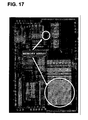
- a memory array shown in FIG. 17 was fabricated by using the PZTN thin films described above.
- L stands for "line” and means a width of the word lines.
- the device had a cross section as shown in FIG. 19; and by irradiating a laser beam with an appropriate wavelength from the side of the glass substrate, H 2 is generated from the TEOS-SiO 2 , and the TFT alone can be separated.
- the mobility was about 500.
- the second gate electrode of the separated TFT was placed on the upper electrode of the PZTN capacitor and both electrodes being Al electrodes were then solid-bonded through pressure-bonding for one hour at 400°C in an N 2 atmosphere in a 971 kPa (9.9 atm) environment.
- FIG. 24 indicates, when the amount of change in the carrier density of the semiconductor substrate is decided by optimizing the dielectric film thickness at the bonded section of the ferroelectric capacitor and the semiconductor substrate, and by optimizing the gate voltage, the different amount of stored charge before and after polarization inversion of the ferroelectric can be sufficiently read out due to the combination of the optimized dielectric film thickness and gate voltage without deteriorating the excellent characteristics of the ferroelectric capacitor or characteristics of the bonded transistor at all.
- a substrate having a Pt/PZTN/Pt/TiOx/SiO 2 /Si structure was heated in N 2 at 400 °C for 10min, and then placed on a stainless steel table to be rapidly cooled, and then its temperature was again elevated at a temperature elevating rate of 10 °C/min to 400 °C. It was found that the TiOx and the lower Pt could be separated from each other, as shown in FIG. 25.
- the above takes advantage of the facts that an Si substrate has a small coefficient of expansion and a high distortion point (temperature at which a distortion takes place) which is as high as about 1000 °C, and ceramics such as PZT have a low distortion point of about 400 °C, and since a ferroelectric capacitor having a distortion has an abnormal expansion, a ferroelectric capacitor can be separated, by using these facts.
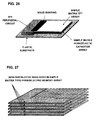
- TFTs and bonded ferroelectric capacitor cells are separated, and a memory device can be formed with them on any substrate such as a plastic substrate, or the like, as shown in FIG. 26.
Landscapes
- Engineering & Computer Science (AREA)
- Computer Hardware Design (AREA)
- Semiconductor Memories (AREA)
- Non-Volatile Memory (AREA)
Abstract
Description
The cell configuration includes one transistor, which is also effective with regard to a greater integration.
- FIG.1
- is a view showing a structure of a ferroelectric capacitor in accordance with an embodiment of the present invention;
- FIG. 2
- is a view showing a P (polarization) - V (voltage) hysteresis curve of the ferroelectric capacitor in accordance with an embodiment of the present invention;
- FIG. 3
- are views showing a structure of a ferroelectric memory device in accordance with an embodiment of the present invention in which memory cells are arranged in a simple matrix, wherein the figure (A) is a plan view thereof and the figure (B) is a cross-sectional view thereof;
- FIG. 4
- is a view showing a TFT cell arrangement formed in a simple matrix in accordance with an embodiment of the present invention;
- FIG. 5
- is a view showing a structure of a non-destructive read system simple matrix type ferroelectric memory in accordance with an embodiment of the present invention in which a simple matrix type ferroelectric capacitor write device, a simple matrix type TFT read device and a peripheral circuit with TFT are solid-bonded together;
- FIG. 6
- is a view showing a structure of a non-destructive read system simple matrix type ferroelectric memory cell in accordance with an embodiment of the present invention;
- FIG. 7
- is a schematic diagram of a simple matrix type ferroelectric memory array in accordance with an embodiment of the present invention;
- FIG. 8
- is a view showing XRD patterns of a PZTN thin film in accordance with an embodiment of the present invention;
- FIG. 9
- is a view showing a hysteresis characteristic of a PZTN thin film in accordance with an embodiment of the present invention;
- FIG. 10
- is a view showing leakage current characteristics of a PZTN thin film in accordance with an embodiment of the present invention;
- FIG. 11
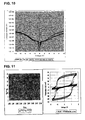
- are views showing fatigue characteristics and static imprint characteristics of PZTN thin films in accordance with an embodiment of the present invention;
- FIG. 12
- is a view showing a structure of a capacitor with an SiO2 protection film formed by ozone TEOS film in accordance with an embodiment of the present invention;
- FIG. 13
- is a view showing capacitor characteristics after an SiO2 protection film is formed by ozone TEOS in accordance with an embodiment of the present invention;
- FIG. 14
- is a view showing leakage current characteristics of conventional PZT thin films in accordance with an embodiment of the present invention;
- FIG. 15
- is a view showing fatigue characteristics of conventional PZT capacitors in accordance with an embodiment of the present invention;
- FIG. 16
- is a view showing static imprint characteristics of a conventional PZT capacitor in accordance with an embodiment of the present invention;
- FIG. 17
- is a metallographical microscope photograph of a ferroelectric memory device in accordance with an embodiment of the present invention in which memory cells are arranged in a simple matrix;
- FIG. 18
- is a fail bit map of a ferroelectric memory device in accordance with an embodiment of the present invention in which memory cells are arranged in a simple matrix;
- FIG. 19
- is a cross-sectional view of a TFT cell formed on a glass substrate in accordance with an embodiment of the present invention;
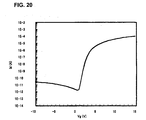
- FIG. 20
- is a view showing Id - Vg characteristics of a TFT formed on a glass substrate in accordance with an embodiment of the present invention;
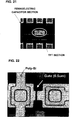
- FIG. 21
- is a metal microscopic photograph of a memory cell in accordance with an embodiment of the present invention in which a ferroelectric capacitor and a TFT are solid-bonded;
- FIG. 22
- is an enlarged metal microscopic photograph of a memory cell in accordance with an embodiment of the present invention in which a ferroelectric capacitor and a TFT are solid-bonded;
- FIG. 23
- is a view showing Id - Vg characteristics of a non-destructive read system simple matrix type ferroelectric memory cell in accordance with an embodiment of the present invention;
- FIG. 24
- is a view showing an operation principle of a non-destructive read system simple matrix type ferroelectric memory cell in accordance with an embodiment of the present invention;
- FIG. 25
- is a TEM photograph of a cross section of a ferroelectric capacitor that is separated by using a difference in coefficients in thermal expansion in accordance with an embodiment of the present invention ;
- FIG. 26
- is a view showing a non-destructive read system simple matrix type ferroelectric memory array formed on a plastic substrate in accordance with an embodiment of the present invention; and
- FIG. 27
- is a view showing a large capacity memory array in accordance with an embodiment of the present invention in which non-destructive read system simple matrix type ferroelectric memory arrays are integrated.

Claims (6)
- A memory device comprising:a semiconductor layer;a source formed in the semiconductor layer;a drain formed in the semiconductor layer, the drain being separated from the source;a gate dielectric layer formed on the semiconductor layer, the gate dielectric layer being formed between the source and the drain;a first gate electrode formed on the gate dielectric layer;a dielectric layer formed below the semiconductor layer;a second gate electrode formed below the dielectric layer; anda ferroelectric capacitor electrically connected to the second gate electrode.
- A memory device as defined in claim 1, having a plurality of the ferroelectric capacitors;
wherein the ferroelectric capacitors are arranged in a simple matrix structure. - A memory device as defined in claim 2, further comprising a plastic substrate provided below the ferroelectric capacitors.
- A method of manufacturing a memory device comprising:forming a first dielectric layer on a glass substrate;forming thin film transistor on the first dielectric layer, the thin film transistor comprising a semiconductor layer;separating the thin film transistor from the first dielectric layer;forming a second dielectric layer on a bottom of the semiconductor layer;forming an electrode below the second dielectric layer;forming a ferroelectric capacitor; andelectrically connecting the electrode to the ferroelectric capacitor.
- A method as defined in claim 4, wherein the ferroelectric capacitor is formed above the first substrate;
further comprising:separating the ferroelectric capacitor from the first substrate; andproviding the ferroelectric capacitor separated from the first substrate on a second substrate. - A method as defined in claim 4 or claim 5, wherein the step of the forming the ferroelectric capacitor comprises forming a ferroelectric layer from a solution; wherein the solution comprises methyl succinate.
Applications Claiming Priority (2)
| Application Number | Priority Date | Filing Date | Title |
|---|---|---|---|
| US10/858,498 US7187575B2 (en) | 2003-04-14 | 2004-06-01 | Memory device and its manufacturing method |
| US858498 | 2004-06-01 |
Publications (2)
| Publication Number | Publication Date |
|---|---|
| EP1603164A2 true EP1603164A2 (en) | 2005-12-07 |
| EP1603164A3 EP1603164A3 (en) | 2007-01-03 |
Family
ID=34936914
Family Applications (1)
| Application Number | Title | Priority Date | Filing Date |
|---|---|---|---|
| EP05011305A Withdrawn EP1603164A3 (en) | 2004-06-01 | 2005-05-25 | Memory device and its manufacturing method |
Country Status (2)
| Country | Link |
|---|---|
| EP (1) | EP1603164A3 (en) |
| CN (1) | CN1707795A (en) |
Families Citing this family (2)
| Publication number | Priority date | Publication date | Assignee | Title |
|---|---|---|---|---|
| WO2013011600A1 (en) * | 2011-07-15 | 2013-01-24 | パナソニック株式会社 | Method for driving semiconductor storage device |
| US11737280B2 (en) * | 2021-03-05 | 2023-08-22 | Taiwan Semiconductor Manufacturing Company, Ltd. | Wakeup free approach to improve the ferroelectricity of FeRAM using a stressor layer |
Family Cites Families (7)
| Publication number | Priority date | Publication date | Assignee | Title |
|---|---|---|---|---|
| US5376561A (en) * | 1990-12-31 | 1994-12-27 | Kopin Corporation | High density electronic circuit modules |
| US5303182A (en) * | 1991-11-08 | 1994-04-12 | Rohm Co., Ltd. | Nonvolatile semiconductor memory utilizing a ferroelectric film |
| JP3424427B2 (en) * | 1995-07-27 | 2003-07-07 | ソニー株式会社 | Nonvolatile semiconductor memory device |
| US6140672A (en) * | 1999-03-05 | 2000-10-31 | Symetrix Corporation | Ferroelectric field effect transistor having a gate electrode being electrically connected to the bottom electrode of a ferroelectric capacitor |
| EP2565924B1 (en) * | 2001-07-24 | 2018-01-10 | Samsung Electronics Co., Ltd. | Transfer method |
| DE10223505A1 (en) * | 2002-05-27 | 2003-12-11 | Infineon Technologies Ag | Method for producing a memory cell, memory cell and memory cell arrangement |
| JP3791614B2 (en) * | 2002-10-24 | 2006-06-28 | セイコーエプソン株式会社 | Ferroelectric film, ferroelectric memory device, piezoelectric element, semiconductor element, piezoelectric actuator, liquid ejecting head, and printer |
-
2005
- 2005-02-17 CN CN200510007770.XA patent/CN1707795A/en active Pending
- 2005-05-25 EP EP05011305A patent/EP1603164A3/en not_active Withdrawn
Non-Patent Citations (1)
| Title |
|---|
| None * |
Also Published As
| Publication number | Publication date |
|---|---|
| EP1603164A3 (en) | 2007-01-03 |
| CN1707795A (en) | 2005-12-14 |
Similar Documents
| Publication | Publication Date | Title |
|---|---|---|
| US6674109B1 (en) | Nonvolatile memory | |
| KR100258751B1 (en) | Nonvolatile memory based on metal-ferroelectric-metal-insulator semiconductor structure | |
| US6121648A (en) | Ferroelectric based memory devices utilizing hydrogen getters and recovery annealing | |
| US20040164342A1 (en) | Integrated circuit memory device and method | |
| US7187575B2 (en) | Memory device and its manufacturing method | |
| JP2010267705A (en) | Semiconductor memory cell and manufacturing method thereof | |
| US6964873B2 (en) | Semiconductor device having a ferroelectric capacitor and a fabrication process thereof | |
| US5977577A (en) | Ferroelectric based memory devices utilizing low curie point ferroelectrics and encapsulation | |
| US7425738B2 (en) | Metal thin film and method of manufacturing the same, dielectric capacitor and method of manufacturing the same, and semiconductor device | |
| US6194751B1 (en) | Ferroelectric based memory devices utilizing low Curie point ferroelectrics and encapsulation | |
| US20020190274A1 (en) | High density single transistor ferroelectric non-volatile memory | |
| US6608339B2 (en) | Ferroelectric memory element | |
| US6080593A (en) | Method of manufacturing ferroelectric memory | |
| US6495412B1 (en) | Semiconductor device having a ferroelectric capacitor and a fabrication process thereof | |
| CN1319256A (en) | Ferroelectric films with reduced tetragonality | |
| EP1603164A2 (en) | Memory device and its manufacturing method | |
| US20050072996A1 (en) | Ferroelectric thin film, method of manufacturing the same, ferroelectric memory device and ferroelectric piezoelectric device | |
| KR100219522B1 (en) | A semiconductor device having single crystal ferroelectric film and fabrication method of the same | |
| JP4459335B2 (en) | Ferroelectric transistor type nonvolatile memory element and manufacturing method thereof | |
| JPH09321237A (en) | Nonvolatile semiconductor memory device having ferroelectric film, capacitor having ferroelectric film, and manufacturing method thereof | |
| KR100363393B1 (en) | Ndro-fram memory cell device and the fabrication method there of | |
| JP3872917B2 (en) | Manufacturing method of semiconductor device | |
| JP3663575B2 (en) | Method for modifying ferroelectric film and method for manufacturing capacitive element | |
| KR20030036405A (en) | Layered structure ferroelectric transistor with GaN substrate and their manufacturing method | |
| KR100470834B1 (en) | Method for fabricating gate stack of ferroelectric memory field effect transistor |
Legal Events
| Date | Code | Title | Description |
|---|---|---|---|
| PUAI | Public reference made under article 153(3) epc to a published international application that has entered the european phase |
Free format text: ORIGINAL CODE: 0009012 |
|
| AK | Designated contracting states |
Kind code of ref document: A2 Designated state(s): AT BE BG CH CY CZ DE DK EE ES FI FR GB GR HU IE IS IT LI LT LU MC NL PL PT RO SE SI SK TR |
|
| AX | Request for extension of the european patent |
Extension state: AL BA HR LV MK YU |
|
| PUAL | Search report despatched |
Free format text: ORIGINAL CODE: 0009013 |
|
| AK | Designated contracting states |
Kind code of ref document: A3 Designated state(s): AT BE BG CH CY CZ DE DK EE ES FI FR GB GR HU IE IS IT LI LT LU MC NL PL PT RO SE SI SK TR |
|
| AX | Request for extension of the european patent |
Extension state: AL BA HR LV MK YU |
|
| RIC1 | Information provided on ipc code assigned before grant |
Ipc: H01L 27/12 20060101ALI20061130BHEP Ipc: H01L 21/84 20060101ALI20061130BHEP Ipc: G11C 11/22 20060101ALI20061130BHEP Ipc: H01L 29/78 20060101ALI20061130BHEP Ipc: H01L 29/51 20060101ALI20061130BHEP Ipc: H01L 21/8246 20060101ALI20061130BHEP Ipc: H01L 27/115 20060101AFI20050817BHEP |
|
| 17P | Request for examination filed |
Effective date: 20070119 |
|
| 17Q | First examination report despatched |
Effective date: 20070219 |
|
| AKX | Designation fees paid |
Designated state(s): DE GB |
|
| STAA | Information on the status of an ep patent application or granted ep patent |
Free format text: STATUS: THE APPLICATION IS DEEMED TO BE WITHDRAWN |
|
| 18D | Application deemed to be withdrawn |
Effective date: 20101202 |