EP1603126A2 - Integrated optical system and method of manufacturing the same and information recording and/or reproducing apparatus using the integrated optical system - Google Patents
Integrated optical system and method of manufacturing the same and information recording and/or reproducing apparatus using the integrated optical system Download PDFInfo
- Publication number
- EP1603126A2 EP1603126A2 EP05253086A EP05253086A EP1603126A2 EP 1603126 A2 EP1603126 A2 EP 1603126A2 EP 05253086 A EP05253086 A EP 05253086A EP 05253086 A EP05253086 A EP 05253086A EP 1603126 A2 EP1603126 A2 EP 1603126A2
- Authority
- EP
- European Patent Office
- Prior art keywords
- optical
- lens
- optical system
- light source
- light
- Prior art date
- Legal status (The legal status is an assumption and is not a legal conclusion. Google has not performed a legal analysis and makes no representation as to the accuracy of the status listed.)
- Withdrawn
Links
Images



Classifications
-
- G—PHYSICS
- G11—INFORMATION STORAGE
- G11B—INFORMATION STORAGE BASED ON RELATIVE MOVEMENT BETWEEN RECORD CARRIER AND TRANSDUCER
- G11B7/00—Recording or reproducing by optical means, e.g. recording using a thermal beam of optical radiation by modifying optical properties or the physical structure, reproducing using an optical beam at lower power by sensing optical properties; Record carriers therefor
- G11B7/12—Heads, e.g. forming of the optical beam spot or modulation of the optical beam
- G11B7/123—Integrated head arrangements, e.g. with source and detectors mounted on the same substrate
-
- G—PHYSICS
- G11—INFORMATION STORAGE
- G11B—INFORMATION STORAGE BASED ON RELATIVE MOVEMENT BETWEEN RECORD CARRIER AND TRANSDUCER
- G11B7/00—Recording or reproducing by optical means, e.g. recording using a thermal beam of optical radiation by modifying optical properties or the physical structure, reproducing using an optical beam at lower power by sensing optical properties; Record carriers therefor
- G11B7/12—Heads, e.g. forming of the optical beam spot or modulation of the optical beam
- G11B7/22—Apparatus or processes for the manufacture of optical heads, e.g. assembly
-
- G—PHYSICS
- G11—INFORMATION STORAGE
- G11B—INFORMATION STORAGE BASED ON RELATIVE MOVEMENT BETWEEN RECORD CARRIER AND TRANSDUCER
- G11B7/00—Recording or reproducing by optical means, e.g. recording using a thermal beam of optical radiation by modifying optical properties or the physical structure, reproducing using an optical beam at lower power by sensing optical properties; Record carriers therefor
- G11B7/12—Heads, e.g. forming of the optical beam spot or modulation of the optical beam
- G11B7/125—Optical beam sources therefor, e.g. laser control circuitry specially adapted for optical storage devices; Modulators, e.g. means for controlling the size or intensity of optical spots or optical traces
- G11B7/126—Circuits, methods or arrangements for laser control or stabilisation
- G11B7/1263—Power control during transducing, e.g. by monitoring
-
- G—PHYSICS
- G11—INFORMATION STORAGE
- G11B—INFORMATION STORAGE BASED ON RELATIVE MOVEMENT BETWEEN RECORD CARRIER AND TRANSDUCER
- G11B7/00—Recording or reproducing by optical means, e.g. recording using a thermal beam of optical radiation by modifying optical properties or the physical structure, reproducing using an optical beam at lower power by sensing optical properties; Record carriers therefor
- G11B7/12—Heads, e.g. forming of the optical beam spot or modulation of the optical beam
- G11B7/13—Optical detectors therefor
- G11B7/131—Arrangement of detectors in a multiple array
-
- G—PHYSICS
- G11—INFORMATION STORAGE
- G11B—INFORMATION STORAGE BASED ON RELATIVE MOVEMENT BETWEEN RECORD CARRIER AND TRANSDUCER
- G11B7/00—Recording or reproducing by optical means, e.g. recording using a thermal beam of optical radiation by modifying optical properties or the physical structure, reproducing using an optical beam at lower power by sensing optical properties; Record carriers therefor
- G11B7/12—Heads, e.g. forming of the optical beam spot or modulation of the optical beam
- G11B7/135—Means for guiding the beam from the source to the record carrier or from the record carrier to the detector
- G11B7/1353—Diffractive elements, e.g. holograms or gratings
-
- G—PHYSICS
- G11—INFORMATION STORAGE
- G11B—INFORMATION STORAGE BASED ON RELATIVE MOVEMENT BETWEEN RECORD CARRIER AND TRANSDUCER
- G11B7/00—Recording or reproducing by optical means, e.g. recording using a thermal beam of optical radiation by modifying optical properties or the physical structure, reproducing using an optical beam at lower power by sensing optical properties; Record carriers therefor
- G11B7/12—Heads, e.g. forming of the optical beam spot or modulation of the optical beam
- G11B7/135—Means for guiding the beam from the source to the record carrier or from the record carrier to the detector
- G11B7/1362—Mirrors
-
- Y—GENERAL TAGGING OF NEW TECHNOLOGICAL DEVELOPMENTS; GENERAL TAGGING OF CROSS-SECTIONAL TECHNOLOGIES SPANNING OVER SEVERAL SECTIONS OF THE IPC; TECHNICAL SUBJECTS COVERED BY FORMER USPC CROSS-REFERENCE ART COLLECTIONS [XRACs] AND DIGESTS
- Y10—TECHNICAL SUBJECTS COVERED BY FORMER USPC
- Y10T—TECHNICAL SUBJECTS COVERED BY FORMER US CLASSIFICATION
- Y10T156/00—Adhesive bonding and miscellaneous chemical manufacture
- Y10T156/10—Methods of surface bonding and/or assembly therefor
- Y10T156/1052—Methods of surface bonding and/or assembly therefor with cutting, punching, tearing or severing
Definitions
- the present invention relates to an information recording and/or reproducing apparatus, and more particularly, to an integrated optical system and a method of manufacturing the same, and an information recording and/or reproducing apparatus employing the integrated optical system.
- the recording capacity is determined according to the size of a focused light spot.
- the size (S) of a focused light spot is determined according to the wavelength ( ⁇ ) of laser light and the numerical aperture (NA) of an objective lens, as expressed below. S ⁇ ⁇ / NA
- CDs compact discs
- an objective lens having an NA of 0.45 or 0.5 to record information thereon and/or reproduce information therefrom
- intensive research has been conducted into increasing the recording density and information storage capacity of the media.
- DVDs Digital versatile discs
- An NA of an objective lens for a high-density optical information storage medium is an NA of 0.65 or 0.85, which will be described later.
- the thickness of a DVD is reduced to 0.6 mm from 1.2 mm of a CD to provide adequate tolerance for tilting of the optical information storage medium because an NA of an objective lens is increased to 0.6 for the DVD from 0.45 for the CD.
- the thickness of the high-density optical information storage medium must be reduced to about 0.1 mm.
- BD Blu-ray Disc
- the wavelength of a light source is 405 nm
- the NA of an objective lens is 0.85.
- the standard thickness of BDs is about 0.1 m.
- HD DVDs are currently under development as high-density optical information storage media.
- HD DVDs have the same substrate thickness and require an objective lens having the same NA as DVDs.
- optical pickups For use in the field of portable terminals, optical pickups should be slim and small and be able to record and/or reproduce a large amount of information, such as music, moving pictures, etc., at high density.
- a conventional optical pickup is constructed by optically aligning and bonding a plurality of individually manufactured optical elements. Therefore, due to possible assembling errors in the assembling and aligning of parts, the reliability of the assembled optical pickup and the degree of automation are lowered.
- an integrated optical system comprising: an optical bench on which a light source generating light and at least one photodetector including a main photodetector receiving the light are mounted; a lens unit coupled to the optical bench; an optical path separating member separating an optical path of light emitted from the light source and propagating toward the lens unit and an optical path of light incident from the lens unit; and an optical path forming unit coupled to the optical bench, the optical path forming unit including a first mirror reflecting the light emitted from the light source to the lens unit, and a second mirror reflecting the light incident from the lens unit and reflected by the first mirror to the main photodetector.
- the at least one photodetector may further include a monitor photodetector disposed on the optical bench and directly receiving some of the light forwardly emitted from the light source.
- the main photodetector and the monitor photodetector may be disposed on a bottom surface of the optical bench, and the light source may be mounted on a mount and spaced apart from the bottom surface of the optical bench.
- the monitor photodetector may be parallel to the light source, slanted toward the light source, or spaced apart from the bottom surface of the optical bench.
- the light source may be mounted on a mount.
- the light source may be interposed between the first and second mirrors.
- the optical path separating member may include a diffraction optical element.
- the optical path separating member may include a polarization diffraction element and a quarter-wave plate.
- a receiving groove with an opening may be formed in the optical bench, and the optical path separating member may be inserted into the receiving groove.
- the integrated optical system may further comprise wires and terminals for electrical connection between the light source and the at least one photodetctor and external circuits, wherein the wires and terminals are formed on a substrate of the optical bench.
- an integrated optical system comprising: an optical bench on which a light source generating light and a monitor photodetector directly receiving some of the light forwardly emitted from the light source are mounted; a lens unit coupled to the optical bench; and an optical path separating member separating an optical path of light emitted from the light source and then propagating toward the lens unit and an optical path of light incident from the lens unit.
- the monitor photodetector may be disposed on a bottom surface of the optical bench, and the light source may be mounted on a mount and spaced apart from the bottom surface of the optical bench.
- the monitor photodetector may be parallel to the light source, slanted toward the light source, or spaced from the bottom surface of the optical bench.
- the light source may be mounted on a mount.
- the integrated optical system may further comprise a main photodetector mounted on the optical bench; and wires and terminals for electrical connection between the light source, the main photodetector, and the monitor photodetector and external circuits, wherein the wires and terminals are formed on a bottom surface of the optical bench.
- the lens unit may include at least one of a refractive lens, a diffractive lens, and a gradient index (GRIN) lens.
- a refractive lens a refractive lens
- a diffractive lens a diffractive lens
- a gradient index (GRIN) lens a gradient index (GRIN) lens
- the lens unit may include a hybrid lens composed of the refractive lens and the diffractive lens.
- the lens unit may include the refractive lens and the diffractive lens, the refractive lens may function as an objective lens, and the diffractive lens may function as a collimating lens.
- the lens unit may be structured such that the diffractive lens functioning as a collimating lens is formed at one surface of a lens holder and conversion can be selectively made between an optical module for an optical pickup and an optical pickup by selectively inserting the refractive lens functioning as an objective lens into the lens holder.
- the lens unit may use the refractive lens, the diffractive lens, or the GRIN lens functioning a collimating lens so that the integrated optical system can be used as an optical module for an optical pickup.
- a method of manufacturing the integrated optical system of claim 1 comprising: preparing an optical bench wafer on which the optical bench is formed and an optical path forming unit wafer on which the optical path forming unit is formed; and bonding the optical path forming unit wafer to the optical bench wafer and dicing the bonded wafers to obtain an optical bench and optical path forming unit assembly.
- a method of manufacturing the integrated optical system of claim 1 comprising: preparing an optical bench wafer on which the optical bench is formed; attaching the optical path forming unit to the optical bench formed on the optical bench wafer; and dicing the optical bench wafer to which the optical path forming unit is attached to obtain an optical bench and optical path forming unit assembly.
- a method of manufacturing the integrated optical system of claim 1 comprising: preparing an optical bench wafer on which the optical bench is formed; dicing the optical bench wafer; and attaching the optical path forming unit to the optical bench to obtain an optical bench and optical path forming unit assembly.
- the optical path forming unit may be formed on a wafer.
- an information recording and/or reproducing apparatus comprising: the integrated optical system of claim 1; an information storage medium rotating unit rotating an information storage medium; a driving unit driving the integrated optical system and the information storage medium rotating unit; and a control unit controlling the driving unit to control focusing and tracking servos.
- the integrated optical system may be used as an optical pickup.
- the information recording and/or reproducing apparatus may further comprise an objective lens focusing incident light on the information storage medium, and the integrated optical system may be used as an optical module.
- the present invention provides an integrated optical system that aims to satisfy the requirements for small, slim device and can be manufactured through a micro-electro-mechanical system (MEMS) process, a method of manufacturing the integrated optical system, and an information recording and/or reproducing apparatus using the integrated optical system as an optical module or an optical pickup.
- MEMS micro-electro-mechanical system
- FIG. 1 is a schematic perspective view of an integrated optical system according to an embodiment of the present invention.
- FIG. 2 is a side view of the integrated optical system of FIG. 1.
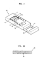
- FIG. 3 is a perspective view of an optical bench 10 of the integrated optical system of FIG. 1.
- the integrated optical system according t the present invention includes the optical bench 10 on which a light source 15 and at least one photodetector including a main photodetector 17 are mounted, a lens unit 70 and an optical path forming unit 30 coupled to the optical bench 10, and an optical path separating member 50 separating an optical path of light emitted from the light source 15 propagating toward the lens unit 70 and an optical path of light reflected by an information storage medium 1and then incident on the lens unit 70.
- the integrated optical system may be used as an optical pickup module or an optical pickup according to the construction of the lens unit 70.
- the at least one photodetector may include the main photodector 17 and a monitor photodetector 19 disposed on the optical bench 10 to directly receive some of the light forwardly emitted from the light source 15.
- the optical bench 10 for example, a silicon optical bench (SiOB), includes the light source 15, the main photodetector 17, and the monitor photodetector 19, which are disposed on a substrate.
- SiOB silicon optical bench
- the substrate of the optical bench 10 may be a silicon wafer.
- the optical bench 10 may be manufactured through a wafer process in which an optical bench wafer is formed using a micro-electro-mechanical system (MEMS) process.
- MEMS micro-electro-mechanical system
- the light source 15 is a semiconductor laser emitting light of a predetermined wavelength.
- the light source 15 may be a semiconductor laser emitting light having a blue wavelength, for example, a wavelength of 405 nm.
- the integrated optical system can record information on and/or reproduce information from a blu-ray disc (BD) or a high definition (HD) DVD.
- BD blu-ray disc
- HD high definition
- the light source 15 may be a semiconductor laser emitting light having a red wavelength, for example, a wavelength of 650 nm.
- the integrated optical system can record information on and/or reproduce information from a digital versatile disc (DVD).
- the light source 15 may be configured to emit light in another wavelength range. Also, the light source 15 may be configured to emit light of a plurality of wavelengths such that the integrated optical system is compatible with a plurality of optical information storage media having different formats.
- the wavelength of light emitted from the light source 15 may vary according to a target information storage medium that is used. Therefore, the integrated optical system can record data on and/or reproduce data from various kinds of optical information storage media, for example, a CD-family optical disc, a DVD-family optical disc, a BD, and/or an HD DVD.
- optical information storage media for example, a CD-family optical disc, a DVD-family optical disc, a BD, and/or an HD DVD.
- the light source 15 may be an edge emitting type semiconductor laser that emits laser light in a direction parallel to semiconductor material layers.
- the light source 15 is mounted on a mount 13. Consequently, the light source 15 is departed apart from a bottom surface 11 of the optical bench 10.
- the light source 15 mounted on the mount 13 may be installed on the optical bench 10.
- the mount 13 may be formed to protrude from the bottom surface 11 of the optical bench 10 and then the light source 15 may be mounted on the mount 13.
- the light source 15, that is, the semiconductor laser may be directly formed on the optical bench wafer for manufacturing the optical bench 10 using a semiconductor process.
- the main photodetector 17 receives the light reflected by the information storage medium 1 and detects an information reproduction (RF) signal and an error signal (e.g., a focusing error signal, a tracking error signal, and/or a tilt error signal) used for servo driving.
- the main photodetector 17 may be disposed on the bottom surface 11 of the optical bench 10.
- the monitor photodetector 19 monitors the intensity of light emitted from the light source 15.
- the monitor photodetector 19 may be disposed in front of the light source 15 to directly receive some of the light forwardly emitted from the light source 15 before the light passes through a reflection mirror.
- the light emitted from the semiconductor laser used as the light source 15 is a diverging light having a Gaussian distribution.
- only central light in a predetermined center region of the diverging light emitted from the semiconductor laser is focused by an objective lens to be used for optical recording and/or reproduction, and peripheral light is not focused by the objective lens and is lost.
- the monitor photodetector 19 receives part of the light with low intensity not focused by the objective lens and monitors the light output from the light source 15. The light received by the monitor photodetector 19 is emitted from the light source 15 and then directly incident on the monitor photodetector 19 without passing through a separate mirror member.
- the monitor photodetector 19 is disposed on the bottom surface 11 of the optical bench in front of the light source 15, the monitor photodetector 19 can receive light with sufficient intensity to monitor the operation of the light source 15.
- the monitor photodetector 19 can be disposed on the bottom surface 11 of the optical bench 10, parallel to the light source 15.
- the monitor photodetector 19 may be slanted toward the light source 15 or may be disposed on a portion protruding from the bottom surface 11 of the optical bench 10. This can be achieved by providing the optical bench 10 with a slanted surface protruding from the bottom surface 11 on which the monitor photodetector 19 is installed, or forming a mount protruding from the bottom surface 11 and having a plane surface parallel to the light source 15. Alternatively, a mount on which the monitor photodetector 19 is mounted may be attached to the optical bench 10.
- the main photodetector 17 and the monitor photodetector 19 may be directly formed on the optical bench wafer on which the optical bench 10 is formed, or may be separately manufactured and then installed on the optical bench 10.
- Wires and pads 23 for electrical connection between the light source 15, the main photodetector 17, and the monitor photodetector 19, and external circuits may be formed on the bottom surface 11 of the optical bench 10.
- the pads 23 are formed to make electrical contact with the external circuits.
- a heating structure (not shown) for radiating heat generated by an actuator (not shown) for driving the integrated optical pickup and/or the light source 15 may be installed on a top surface of the optical bench 10.
- a heating structure may be further installed on a side surface of the optical bench 10, if necessary.
- a receiving groove 25 with an opening 27 is formed at a side of the optical bench 10.
- the optical path separating member 50 may be inserted into the receiving groove 25.
- the optical path separating member 50 separates the optical paths of the light emitted from the light source 15 and proceeding toward the lens unit 70 and the light incident from the lens unit 70.
- the receiving groove 25 with the opening 27 may be formed in the optical bench 10, and the optical path separating member 50 may be inserted into the receiving groove 25.
- the optical path separating member 50 may be attached to a surface of the optical bench 10 with no receiving groove, or the optical path separating member 50 may be integrally formed with the lens unit 70.
- the optical bench 10 have the opening 27 through which the light emitted from the light source 15 and then reflected by a first mirror 31 of the optical path forming unit 30 can pass to propagate toward the lens unit 70.
- the optical path separating member 50 separates optical paths by transmitting light directed to the information storage medium 1 without altering the light's path and diffracting light reflected by the information storage medium 1.
- the optical path separating member 50 allows the detection of a signal recorded on the information storage medium 1 and focusing and tracking error signals by diffracting the light reflected by the information storage medium 1 into a plurality of light beams, or adjusting a shape of a light spot formed on the main photodetector 17 and reflecting light to the main photodetector 17 for signal detection.
- FIG. 4A illustrates an example where the optical path separating member 50 has a diffraction optical element 51, for example, a hologram optical element (HOE) or a diffractive optical element (DOE).
- a diffraction optical element 51 for example, a hologram optical element (HOE) or a diffractive optical element (DOE).
- HOE hologram optical element
- DOE diffractive optical element
- the optical path separating member 50 When the optical path separating member 50 has the diffraction optical element 51, the light reflected by the information storage medium 1 is diffracted by the optical path separating member 50 at an angle such that the light proceeds toward the main photodetector 17 distanced from the light source 15.
- the integrated optical system according to the present invention may include a polarization selectivity optical path separating member 150 as shown in FIG. 4B instead of the optical path separating member 50 with the diffraction optical element 51.
- the polarization selectivity optical path separating member 150 includes a polarization diffraction element 151, which is a polarization holographic element, selectively straightly transmitting or diffractively transmitting incident light depending on the polarization of the incident light, and a quarter-wave plate 153, which changes the polarization of the incident light.
- a polarization diffraction element 151 which is a polarization holographic element, selectively straightly transmitting or diffractively transmitting incident light depending on the polarization of the incident light
- a quarter-wave plate 153 which changes the polarization of the incident light.
- the semiconductor laser used as the light source 15 emits laser light having a predominant linearly polarized component. Thus, substantially s-polarized or p-polarized light may be emitted from the semiconductor laser.
- the polarization diffraction element 151 is configured to transmit linearly polarized light emitted from the light source 15 without altering the light's path
- the light transmitted through the polarization diffraction element 151 is changed into first circularly polarized light after passing through the quarter-wave plate 153 and then into second circularly polarized light, which is orthogonal to the first circularly polarized light, after being reflected by the optical information storage medium 1.
- the second circularly polarized light is changed into another linearly polarized light after passing through the quarter-wave plate 153 and then is diffracted by the polarization diffraction element 151.
- the optical path of the light proceeding toward the optical information storage medium 1 and the optical path of the light reflected by the optical information storage medium 1 can be separated from one another by the polarization selectivity optical path separating member 150.
- the polarization selectivity optical path separating member 150 diffracts only the light reflected by the information storage medium 1, without affecting the light emitted directly from the light source 15, thereby increasing efficiency.
- the optical path forming unit 30 includes the first mirror 31, which reflects the light emitted from the light source 15 to the lens unit 70, and a second mirror 35, which reflects the light incident from the lens unit 70 reflected by the first mirror 31 to the main photodetector 17.
- the light source 15 may be disposed between the first and second mirrors 31 and 35.
- the optical path forming unit 30 comprises the two mirrors 31 and 35 as shown in FIGS. 1 and 2, and is adapted to form an optical path of the light emitted from the light source 15 such that a focal point is formed on the information storage medium 1 through the objective lens of the lens unit 70 and to transmit the light reflected by the information storage medium 1 to the main photodetector 17.
- the optical path forming unit 30 may be manufactured using a wafer process. That is, as described later, the optical path forming unit 30 may be formed by processing a plurality of mirrors on an optical path forming unit wafer.
- An optical bench and optical path forming unit assembly may be formed by bonding the optical path forming unit wafer on which the at least one optical path forming unit 30 is formed to the optical bench wafer and dicing the bonded wafers, or the optical path forming unit 30 may be formed by dicing the optical path forming unit wafer by mirrors and then attaching the mirrors at proper positions to the optical bench 10.
- the lens unit 70 may be coupled to one side of the top surface of the optical bench 10.
- the lens unit 70 may include at least one of a refractive lens, a diffractive lens, and a gradient index (GRIN) lens.
- GRIN gradient index
- the lens unit 70 may include a hybrid lens composed of a refractive lens 71 and a diffractive lens 73.
- the refractive lens 71 may be inserted into a lens holder 75 and the diffractive lens 73 may be formed at one surface of the lens holder 75.
- the lens unit 70 may be formed by perforating a silicon substrate to form the lens holder 75 having an opening to assemble the refractive lens 71, forming the diffractive lens 73 on a glass substrate, inserting the refractive lens 71 into the opening of the lens holder 75, and attaching the diffractive lens 73 to one surface of the lens holder 75.
- An objective lens focuses the light emitted from the light source 15 and forms a light spot smaller than a diffraction limit to record a signal on the information storage medium 1 and read the recorded signal.
- the refractive lens 71 and the diffractive lens 73 may be designed to function as an objective lens for incident diverging light. Accordingly, if the hybrid lens composed of the diffractive lens 73 and the refractive lens 71 is used as the objective lens, the refractive lens 71 can be easily manufactured and better correction of chromatic aberration can be achieved.
- the refractive lens 71 and the diffractive lens 73 are independent parts in FIG. 5, the hybrid lens composed of the refractive lens 71 and the diffractive lens 73 that are integrally formed with each other may be used as the objective lens.
- the diffractive lens 73 may be formed at a bottom surface of the lens holder 75.
- the diffractive lens 73 may be designed to collimate a beam.
- the diffractive lens 73 functions as a collimating lens that collimates incident diverging light, and the refractive lens 71 functions as an objective lens that focuses the light collimated by the diffractive lens 73.
- the hybrid lens can relieve aberration, such as chromatic aberration and spherical aberration, whether the hybrid lens acts as both an objective lens and a collimating lens or acts as only an objective lens.
- the diffractive lens 73 has a greater diffraction angle with respect to longer wavelength light
- the refractive lens 71 has a smaller refraction angle with respect to longer wavelength light. Accordingly, by combining the diffractive lens 73 and the refractive lens 71, an occurrence of chromatic aberration due to a variation in the wavelength of light can be suppressed.
- the lens unit 70 functions as a collimating lens in the state where the refractive lens 71 is not assembled into the lens holder 75, as shown in FIG. 6.
- the integrated optical system according to the present invention can be used as an integrated optical pickup as illustrated in FIG. 7.
- the integrated optical system according to the present invention may be used as an optical pickup module for an optical pickup as shown in FIG. 8.
- FIG. 7 is a diagram illustrating an example where the integrated optical system according to the present invention is used as an integrated optical pickup.
- the lens unit 70 includes both the refractive lens 71 and the diffractive lens 73 shown in FIG. 5.
- the integrated optical system When the integrated optical system is used as the integrated optical pickup as shown in FIG. 7, the whole integrated optical system is focused, tracked, and/or titled by the actuator.
- FIG. 8 is a diagram illustrating an example where the integrated optical system according to the present invention is used as the optical module for an optical pickup.
- the lens unit 70 may include the diffractive lens 73 designed to act as a collimating lens but not include the refractive lens 71 designed to act as an objective lens.
- the diffractive lens 73 designed to act as a collimating lens may be formed on a separate substrate and attached to the opening of the optical bench 10 or may be integrally formed with the optical path separating member 50.
- the lens unit 70 may use a refractive lens, a diffractive lens, or a GRIN lens as the collimating lens, and in this case, the integrated optical system can be used as an optical module for an optical module.
- the optical pickup may further include a reflection mirror 81 reflecting light emitted from the optical module and an objective lens 85 focusing the light reflected by the reflection mirror 81 and forming a spot on the information storage medium 1.
- the objective lens 85 can be focused, tracked, and/or tilted by the actuator.
- the integrated optical system according to the present invention can be easily converted between the optical pickup and the optical module for an optical pickup during manufacturing. That is, the integrated optical system can be selectively used as the optical module for the optical pickup or the optical pickup by selectively inserting the refractive lens 71 into the lens holder 75 having one surface on which the diffractive lens 73 is formed.
- the lens unit 70 can be easily coupled to the optical bench 10 by simply attaching the lens holder 75 to the optical bench 10.
- the diffractive lens 73 is used in the above description, a refractive lens functioning as a collimating lens may be used instead of the diffractive lens 73.
- the objective lens that is, the refractive lens 71 functioning as the objective lens of the lens unit 70 or the separate objective lens 85 (see FIG. 8).
- Light reflected by the information storage medium 1 passes through the objective lens, is divided into a plurality of beams or is adjusted the shape of a spot focused on the main photodetector 17, and is changed proceeding direction by the optical path separating member 50, is reflected by the first mirror 31, and reaches the second mirror 35 without interfering with the light source 15 and the sub mount 13 of the light source 15.
- Light reflected by the second mirror 35 is formed on the main photodetector 17 for signal detection to detect a signal recorded on the information storage medium 1 and/or focusing and tracking errors of the information storage medium 1.
- the integrated optical system according to the present invention has a simpler structure than a conventional optical pickup, and a MEMS process can be used to manufacture most parts, that is, the optical bench and the optical path forming unit of the integrated optical system, a plurality of the integrated optical systems can be simultaneously manufactured on a wafer, and can be more easily adjusted and assembled than for a conventional optical pickup. Also, since the structure is simple and the most parts are integrated, the size of the optical pickup can be reduced.
- the optical bench 10 can be manufactured as follows. After the main photodetector 17 and the monitor photodetector 19 are directly formed on the optical bench wafer, the internal wires 21 and the pads 23 are formed through a thin film process. To mount the light source 15, that is, the semiconductor laser, on the optical bench 10, the sub mount 13 to which the light source 15 is bonded is manufactured, and the sub mount 13 is bonded to the bottom surface 11 of the optical bench 10 on which the main photodetector 17 and the monitor photodetector 19 are disposed. The wires 21 are completed by wire bonding, if necessary. Alternatively, the main photodetector 17 and the monitor photodetector 19 may be separately manufactured and then bonded to the bottom surface 11 of the optical bench 10, and the light source 15 may be directly formed on the optical bench 10 through a semiconductor process.
- the light source 15 may be directly formed on the optical bench 10 through a semiconductor process.
- the optical path forming unit 30 comprising the first and second mirrors 31 and 35 is manufactured through a wafer process, that is, the first and second mirrors 31 and 35 are in array formed on the wafer by etching the optical path forming unit wafer or molding polymer or glass.
- the optical path forming unit wafer and the optical bench wafer are aligned, bonded, and diced to obtain an optical bench and optical path forming unit assembly.
- the integrated optical system used as the optical pickup or the optical module can be manufactured.
- the lens unit 70 and the optical path separating member 50 are coupled to the optical bench 10 by centering the lens unit 70 (e.g., the objective lens) and adjusting the optical path separating member 50 and the lens unit 70 so that light can be properly received by the main photodetector 17.
- the lens unit 70 and the optical path separating member 50 are coupled to the optical bench 10 through this adjustment process, the integrated optical system according to the present invention is obtained.
- the optical bench wafer on which the optical bench 10 is formed is prepared, and mirrors which are manufactured through a wafer process or are separately manufactured are attached at appropriate positions to the optical bench 10 on the optical bench wafer to form a structure in which the first and second mirrors 31 and 35 of the optical path forming unit 30 are attached to the optical bench 10. Subsequently, the optical bench wafer to which the optical path forming unit 30 is attached is diced to obtain an optical bench and optical path forming unit assembly.
- the mirrors 31 and 35 constituting the optical path forming unit 30 may be processed in an array from on the optical path forming unit wafer through a wafer process.
- the optical path forming unit wafer is diced into mirrors, the mirrors are separated and then attached at appropriate positions to the optical bench wafer, and the optical bench wafer is diced, to obtain the optical bench and optical path forming unit assembly.
- the optical bench wafer may be first diced, and the mirrors may be attached at appropriate positions to each of the optical benches, to obtain an optical bench and optical path forming unit assembly.
- the objective lens of the lens unit 70 may be first fixed to the optical bench 10 and then the first and second mirrors 31 and 35 of the optical path forming unit 30 may be attached to the optical bench 10.
- the position of the first mirror 31 is determined according to the position of the objective lens.
- the optical path separating member 50 is adjusted so that the main photodetector 17 can properly receive light and the optical path separating member 50 can be inserted into the optical bench 10 to obtain the integrated optical system according to the present invention.
- the objective lens and the optical path separating member 50 may be first fixed to the optical bench 10 and then the first mirror 31 and the second mirror 35 may be attached to the optical bench 10.
- the position of the first mirror 31 is determined according to the position of the objective lens and the position of the second mirror 35 is determined so that light can be properly received by the main photodetector 17.
- the monitor photodetector 19 is disposed in front of the light source as described above.
- FIGS. 9 through 11 respectively illustrate examples in which the monitor photodetector 19 is disposed on the bottom surface 11 of the optical bench 10 and parallel to the light source 15, the monitor photodetector 19 is slanted toward the light source 15, and the monitor photodetector 19 is disposed on a portion protruding from the bottom surface 11 of the optical bench 10 and parallel to the light source 15.
- FIGS. 9 through 11 illustrate examples in which the width of the effective light receiving area of the monitor photodetector 19 is 0.7 mm. Referring to FIGS.
- LD denotes a light emitting point of the light source
- MPD denotes the monitor photodetector
- effective beam area denotes the portion of the beam used for information recording and/or reproduction
- beam area incident on MPD denotes the portion of the beam incident on the effective light receiving area of the monitor photodetector 19.
- Table 1 shows the ratios of the intensity of light received by the monitor photodetector 19 to the total light emitted from the light source 15 respectively when the monitor photodetector 19 is positioned relatively to the light source 19 as shown in FIGS. 9 through 11 and the effective light receiving area of the monitor photodetector 19 is 0.7 mm and 0.5 mm.
- Position of MPD Ratio of amount of light (energy) received by MPD MPD effective light receiving area ⁇ 0.7 mm
- MPD effective light receiving area ⁇ 0.5 mm Disposed on bottom surface and parallel to LD 6.9 % 4.75 % Slanted toward LD 23.1 % 22.58 % Disposed on portion protruding from bottom surface of optical bench and parallel to LD 17.96 % 13.58 %
- the ratio of the amount of light received by the monitor photodetector 19 is 6.9 %, 23.1 %, and 17.96 % respectively in FIGS. 9, 10, and 11.
- the width of the effective light receiving area of the monitor photodetector 19 is 0.5 mm
- the ratio of the intensity of light received by the monitor photodetector 19 is 4.75 %, 22.58 %, and 13.58 % respectively in FIGS. 9, 10, and 11.
- the monitor photodetector 19 when the monitor photodetector 19 is disposed on the bottom surface 11 of the optical bench 10, which is spaced 2.085 mm from the light source 15 so that the width of the effective light receiving area is 0.7 mm, the ratio of light received by the monitor photodetector 19 is 6.9 %. Accordingly, light of sufficient amount for monitoring can be received.
- the width of the effective light receiving area may be less than 0.7 mm. Further, if the monitor photodetector 19 is brought closer to the light source 15, the width of the effective light receiving area may be greater than 0.7 mm.
- FIG. 9 illustrates a specific design example. Accordingly, the distance between the monitor photodetector 19 and the light source 15, and the effective light receiving area are not limited to the example illustrated in FIG. 9, and various modifications can be made within a range where light of sufficient amount for monitoring can be received.
- the ratio of light received by the monitor photodetector 19 is 23.1 %.
- the ratio of light received by the monitor photodetector 19 is 22.58 %.
- the monitor photodetector 19 When the monitor photodetector 19 is slanted toward the light source 15 as shown in FIG. 10, even if the amount of light received by the monitor photodetector 19 is reduced, monitoring can be conducted. Accordingly, the monitor photodetector 19 may be slanted at an angle less than 15 degrees or the monitor photodetector 19 may be positioned closer to the light source 15.
- FIG. 10 just illustrates a specific design example. Accordingly, the distance between the monitor photodetector 19 and the light source 15, the effective light receiving area, and the slanting angle of the monitor photodetector 19 are not limited to the example illustrated in FIG. 10, and various modifications can be made within a range where light of sufficient amount for monitoring can be received.
- the ratio of light received by the monitor photodetector 19 is 17.96 %. Under the same conditions, when the width of the effective light receiving area of the monitor photodetector 19 is 0.5 mm, the ratio of light received by the monitor photodetector 19 is 13.58 %.
- the monitor photodetector 19 When the monitor photodetector 19 is disposed at the portion protruding from the bottom surface 11 of the optical bench 10 as shown in FIG. 11, even if the amount of light received by the monitor photodetector 19 is reduced, monitoring can be conducted. Accordingly, the protrusion of the monitor photodetector 19 may be less than 0.218 mm as indicated in FIG. 11, or the monitor photodetector 19 may be closer to the light source 15.
- FIG. 11 just illustrates a specific design example.
- the distance between the monitor photodetector 19 and the light source 15, the distance between the monitor photodetector 19 and the bottom surface 11 of the optical bench 10, and the effective light receiving area are not limited to the example illustrated in FIG. 11, and various modifications can be made within a range where light of sufficient amount for monitoring can be received.
- the monitor photodetector 19 may be disposed on the bottom surface 11 of the optical bench 10 in front of the light source 15, and in this case, the structure to dispose the monitor photodetector 19 can be simple.
- monitor photodetector 19 may be slanted toward the light source 15, or disposed on the portion protruding from the bottom surface 11 of the optical bench 10.
- FIG. 12 is a schematic view of an information recording and/or reproducing apparatus employing the integrated optical system according to the present invention.
- the information recording and/or reproducing apparatus includes a rotating unit including a spindle motor 455 rotating an information storage medium 1 (e.g., an optical disc), an optical pickup 400 installed to be movable in a radial direction of the information storage medium 1 and reproducing information recorded on the information storage medium 1 and/or recording information, a driving unit 457 driving the rotating unit and the optical pickup 400, and a control unit 470 controlling the driving unit 457 to control focusing and tracking servos of the optical pickup 450.
- the apparatus further includes a turntable 452, and a clamp 453 chucking the information storage medium 1.
- the optical pickup 400 includes the integrated optical system according to the present invention. That is, the optical pickup 400 may be the integrated optical system according to the present invention when the integrated optical system is formed to function as an optical pickup as shown in FIG. 7.
- the optical pickup 400 may include the integrated optical system according to the present invention when the integrated optical system is formed to function as an optical module as shown in FIG. 8.
- Light reflected by the information storage medium 1 is detected by the main photodetector 17 mounted on the optical pickup 400 and converted into an electrical signal through photoelectric conversion.
- the electrical signal is input to the control unit 459 via the driving unit 457.
- the driving unit 457 controls the rate of rotation of the spindle motor 455, amplifies the input signal, and drives the optical pickup 400.
- the control unit 459 transmits a focusing servo command and a tracking servo command, which are adjusted based on the signal input from the driving unit 457, to the driving unit 457 again to implement a focusing and tracking servo operation of the optical pickup 400. Further, the control unit 459 uses the light amount signal detected by the monitor photodetector 19 and controls the light output from the light source 15 so that light of proper amount can be emitted from the light source 15.
- the information recording and/or reproducing apparatus employing the optical pickup according to the present invention can be applied to a portable terminal, such as a personal digital assistant (PDA), a mobile phone, a digital camera, a portable disc player, or a camcorder.
- a portable terminal such as a personal digital assistant (PDA), a mobile phone, a digital camera, a portable disc player, or a camcorder.
- the integrated optical system according to the present invention can satisfy requirements for small, slim devices, and can be integrated using a MEMS process, a plurality of integrated optical systems can be simultaneously manufactured on a wafer and can be more easily adjusted and assembled than conventional optical pickups. Additionally, since the structure is simple and most of the parts can be integrated, the size of the optical pickup can be reduced.
- the integrated optical system according to the present invention can be easily converted for use as an optical module and an integrated optical pickup according to the formation of the diffractive lens and the existence of the refractive lens.
Landscapes
- Physics & Mathematics (AREA)
- Optics & Photonics (AREA)
- Optical Head (AREA)
- Polarising Elements (AREA)
- Diffracting Gratings Or Hologram Optical Elements (AREA)
- Optical Couplings Of Light Guides (AREA)
Abstract
Description
| Position of MPD | Ratio of amount of light (energy) received by MPD | |
| MPD effective light receiving area Φ=0.7 mm | MPD effective light receiving area Φ=0.5 mm | |
| Disposed on bottom surface and parallel to LD | 6.9 % | 4.75 % |
| Slanted toward LD | 23.1 % | 22.58 % |
| Disposed on portion protruding from bottom surface of optical bench and parallel to LD | 17.96 % | 13.58 % |
Claims (30)
- An integrated optical system comprising:an optical bench on which a light source generating light and at least one photodetector including a main photodetector receiving the light are mounted;a lens unit coupled to the optical bench;an optical path separating member separating an optical path of light emitted from the light source and propagating toward the lens unit and an optical path of light incident from the lens unit; andan optical path forming unit coupled to the optical bench, the optical path forming unit including a first mirror reflecting the light emitted from the light source to the lens unit, and a second mirror reflecting the light incident from the lens unit and reflected by the first mirror to the main photodetector.
- The integrated optical system of claim 1, wherein the at least one photodetector further includes a monitor photodetector disposed on the optical bench and directly receiving some of the light forwardly emitted from the light source.
- The integrated optical system of claim 2, wherein the main photodetector and the monitor photodetector are disposed on a bottom surface of the optical bench, and the light source is mounted on a mount and spaced apart from the bottom surface of the optical bench.
- The integrated optical system of claim 2 or 3, wherein the monitor photodetector is parallel to the light source, slanted toward the light source, or spaced apart from the bottom surface of the optical bench.
- The integrated optical system of any preceding claim, wherein the light source is mounted on a mount.
- The integrated optical system of any preceding claim, wherein the light source is interposed between the first and second mirrors.
- The integrated optical system of any preceding claim, wherein the optical path separating member includes a diffraction optical element.
- The integrated optical system of any preceding claim, wherein the optical path separating member includes a polarization diffraction element and a quarter-wave plate.
- The integrated optical system of any preceding claim, wherein a receiving groove with an opening is formed in the optical bench, and the optical path separating member is inserted into the receiving groove.
- The integrated optical system of any preceding claim, further comprising wires and terminals for electrical connection between the light source and the at least one photodetector and external circuits, wherein and the wires and terminals are formed on a substrate of the optical bench.
- The integrated optical system of any preceding claim, wherein an opening through which the light emitted from the light source and reflected by the first mirror passes toward the lens unit is formed in the optical bench.
- An integrated optical system comprising:an optical bench on which a light source generating light and a monitor photodetector directly receiving some of the light forwardly emitted from the light source are mounted;a lens unit coupled to the optical bench; andan optical path separating member separating an optical path of light emitted from the light source and then propagating toward the lens unit and an optical path of light incident from the lens unit.
- The integrated optical system of claim 12, wherein the monitor photodetector is disposed on a bottom surface of the optical bench, and the light source is mounted on a mount and spaced apart from the bottom surface of the optical bench.
- The integrated optical system of claim 13, wherein the monitor photodetector is parallel to the light source, slanted toward the light source, or spaced from the bottom surface of the optical bench.
- The integrated optical system of any of claims 12 to 14, wherein the light source is mounted on a mount.
- The integrated optical system of any of claims 12 to 15, further comprising a main photodetector mounted on the optical bench; and
wires and terminals for electrical connection between the light source, the main photodetector and the monitor photodetector and external circuits, the wires and terminals are formed on a bottom surface of the optical bench. - The integrated optical system of any one of claims 1 through 16, wherein the lens unit includes at least one of a refractive lens, a diffractive lens, and a gradient index (GRIN) lens.
- The integrated optical system of claim 17, wherein the lens unit includes a hybrid lens composed of the refractive lens and the diffractive lens.
- The integrated optical system of claim 17, wherein the lens unit includes the refractive lens and the diffractive lens, the refractive lens functions as an objective lens, and the diffractive lens functions as a collimating lens.
- The integrated optical system of claim 17, wherein the lens unit uses the refractive lens, the diffractive lens, or the GRIN lens functioning a collimating lens so that the integrated optical system can be used as an optical module for an optical pickup.
- The integrated optical system of claim 17, wherein the lens unit is structured such that the diffractive lens functioning as a collimating lens is formed at one surface of a lens holder and conversion can be selectively made between an optical module for an optical pickup and an optical pickup by selectively inserting the refractive lens functioning as an objective lens into the lens holder.
- A method of manufacturing the integrated optical system of any one of claims 1 through 16, the method comprising:preparing an optical bench wafer on which the optical bench is formed and an optical path forming unit wafer on which the optical path forming unit is formed; andbonding the optical path forming unit wafer to the optical bench wafer and dicing the bonded wafers to obtain an optical bench and optical path forming unit assembly.
- A method of manufacturing the integrated optical system of any one of claims 1 through 16, the method comprising:preparing an optical bench wafer on which the optical bench is formed;attaching the optical path forming unit to the optical bench formed on the optical bench wafer; anddicing the optical bench wafer to which the optical path forming unit is attached to obtain an optical bench and optical path forming unit assembly.
- The method of claim 23, wherein the optical path forming unit is formed on a wafer.
- A method of manufacturing the integrated optical system of any one of claims 1 through 16, the method comprising:preparing an optical bench wafer on which the optical bench is formed;dicing the optical bench wafer; andattaching the optical path forming unit to the optical bench to obtain an optical bench and optical path forming unit assembly.
- An information recording and/or reproducing apparatus comprising:the integrated optical system of any one of claims 1 through 16;an information storage medium rotating unit rotating an information storage medium;a driving unit driving the integrated optical system and the information storage medium rotating unit; anda control unit controlling the driving unit to control focusing and tracking servos.
- The information recording and/or reproducing apparatus of claim 26, wherein the lens unit includes a hybrid lens composed of a refractive lens and a diffractive lens, and the integrated optical system is used as an optical pickup.
- The information recording and/or reproducing apparatus of claim 26, wherein the lens unit includes a refractive lens functioning as an objective lens and a diffractive lens functioning as a collimating lens, the refractive lens is inserted into a lens holder, the diffractive lens is disposed at one surface of the lens holder, and the integrated optical system is used as an optical pickup.
- The information recording and/or reproducing apparatus of claim 26, further comprising an objective lens focusing incident light on the information storage medium, wherein the lens unit functions as a collimating lens, and the integrated optical system is used as an optical module.
- The information recording and/or reproducing apparatus of claim 29, wherein the lens unit comprises a diffractive lens functioning as a collimating lens formed at one surface of a lens holder.
Applications Claiming Priority (2)
| Application Number | Priority Date | Filing Date | Title |
|---|---|---|---|
| KR1020040039627A KR100601955B1 (en) | 2004-06-01 | 2004-06-01 | Integrated optical system and its manufacturing method and information recording and / or reproducing apparatus using the same |
| KR2004039627 | 2004-06-01 |
Publications (2)
| Publication Number | Publication Date |
|---|---|
| EP1603126A2 true EP1603126A2 (en) | 2005-12-07 |
| EP1603126A3 EP1603126A3 (en) | 2007-04-04 |
Family
ID=34941379
Family Applications (1)
| Application Number | Title | Priority Date | Filing Date |
|---|---|---|---|
| EP05253086A Withdrawn EP1603126A3 (en) | 2004-06-01 | 2005-05-19 | Integrated optical system and method of manufacturing the same and information recording and/or reproducing apparatus using the integrated optical system |
Country Status (5)
| Country | Link |
|---|---|
| US (2) | US7558161B2 (en) |
| EP (1) | EP1603126A3 (en) |
| JP (1) | JP4206081B2 (en) |
| KR (1) | KR100601955B1 (en) |
| CN (1) | CN100382168C (en) |
Cited By (1)
| Publication number | Priority date | Publication date | Assignee | Title |
|---|---|---|---|---|
| EP1672625A3 (en) * | 2004-12-14 | 2006-08-16 | Samsung Electro-Mechanics Co., Ltd. | Optical bench, integrated optical system, and optical alignment method |
Families Citing this family (6)
| Publication number | Priority date | Publication date | Assignee | Title |
|---|---|---|---|---|
| JP2008152849A (en) * | 2006-12-15 | 2008-07-03 | Sharp Corp | Optical pickup device and photodetector |
| EP1953746A3 (en) * | 2007-02-01 | 2009-11-04 | Ricoh Company, Ltd. | Lens actuator, optical pickup device, and optical recording and reproducing apparatus |
| TWI413118B (en) * | 2011-02-23 | 2013-10-21 | Univ Nat Chiao Tung | Optical pickup head |
| CN110068447B (en) * | 2018-01-23 | 2021-07-27 | 舜宇光学(浙江)研究院有限公司 | Integrated Diffractive Optical Element Test Equipment |
| CN109445123A (en) * | 2018-12-13 | 2019-03-08 | 昆山丘钛微电子科技有限公司 | Emitter and depth camera including the emitter |
| KR102506645B1 (en) * | 2019-10-28 | 2023-03-07 | 한국전자통신연구원 | Cooling optical transmission module device and manufacturing method thereof |
Family Cites Families (32)
| Publication number | Priority date | Publication date | Assignee | Title |
|---|---|---|---|---|
| JPS63237491A (en) | 1987-03-25 | 1988-10-03 | Sony Corp | Manufacture of optical device |
| JPS6412221U (en) | 1987-07-07 | 1989-01-23 | ||
| JPS6427045A (en) | 1987-07-22 | 1989-01-30 | Mitsubishi Electric Corp | Semiconductor device |
| JPS6427045U (en) | 1987-08-05 | 1989-02-16 | ||
| US5317551A (en) * | 1990-07-16 | 1994-05-31 | Matsushita Electric Industrial Co., Ltd. | Optical disk head including a light path having a thickness and width greater than the light beam wavelength by a predetermined amount |
| JPH0479050A (en) | 1990-07-20 | 1992-03-12 | Sharp Corp | Optical pickup device for magneto-optical recording and reproducing device |
| JPH0489634A (en) | 1990-07-25 | 1992-03-23 | Pioneer Electron Corp | Optical pickup device |
| JPH04332185A (en) * | 1991-05-07 | 1992-11-19 | Seiko Epson Corp | Forward emitted light detection mechanism and light intensity adjustment method for semiconductor laser |
| CA2088701C (en) * | 1992-02-05 | 1998-01-27 | Yoshio Yoshida | Optical information reproducing apparatus |
| JPH0721581A (en) * | 1993-06-30 | 1995-01-24 | Sharp Corp | Optical pickup |
| JPH07176070A (en) * | 1993-12-20 | 1995-07-14 | Matsushita Electric Ind Co Ltd | Floating optical head and optical recording / reproducing device |
| JPH07201065A (en) | 1993-12-28 | 1995-08-04 | Nec Corp | Optical recording and reproducing device |
| JPH08115532A (en) * | 1994-10-18 | 1996-05-07 | Matsushita Electric Ind Co Ltd | Optical integrated device, integrated optical pickup device and optical disc device using the same |
| JPH08124205A (en) | 1994-10-27 | 1996-05-17 | Sanyo Electric Co Ltd | Optical pickup |
| US5689108A (en) * | 1995-05-27 | 1997-11-18 | Victor Company Of Japan, Ltd. | Integrated optical pick-up |
| JP3233837B2 (en) | 1995-10-05 | 2001-12-04 | 松下電器産業株式会社 | Semiconductor laser device and optical pickup device |
| JP3440679B2 (en) | 1996-03-01 | 2003-08-25 | ソニー株式会社 | Semiconductor device |
| US5912872A (en) * | 1996-09-27 | 1999-06-15 | Digital Optics Corporation | Integrated optical apparatus providing separated beams on a detector and associated methods |
| US6185239B1 (en) * | 1997-01-22 | 2001-02-06 | Sony Corporation | Semiconductor laser device |
| JPH11273136A (en) * | 1998-03-24 | 1999-10-08 | Matsushita Electric Ind Co Ltd | Optical pickup device |
| US6188062B1 (en) * | 1998-04-08 | 2001-02-13 | Hoetron, Inc. | Laser/detector hybrid with integrated mirror and diffracted returned beam |
| US6351443B1 (en) * | 1999-11-04 | 2002-02-26 | Industrial Technology Research Institute | Diffractive stack pickup head for optical disk drives and method to fabricate the pickup head |
| JP2003523036A (en) | 1999-12-07 | 2003-07-29 | データプレイ・インコーポレイテッド | Thin optical head |
| US6717893B1 (en) * | 2000-10-04 | 2004-04-06 | Dphi Acquisitions, Inc. | Laser thermal management system |
| US6873580B2 (en) * | 2001-05-01 | 2005-03-29 | Dphi Acquisitions, Inc. | Objective lens alignment in optical pickup unit assembly |
| JP2002335032A (en) | 2001-05-08 | 2002-11-22 | Sony Corp | Optical device and method of manufacturing the same |
| JP3743359B2 (en) | 2001-11-30 | 2006-02-08 | 松下電器産業株式会社 | Optical pickup device |
| JP2003257064A (en) * | 2002-03-01 | 2003-09-12 | Sharp Corp | Optical pickup device |
| JP3716805B2 (en) * | 2002-03-18 | 2005-11-16 | 日本ビクター株式会社 | Optical pickup device |
| JP2004127339A (en) * | 2002-09-30 | 2004-04-22 | Asahi Glass Co Ltd | Optical head device |
| KR20040079555A (en) * | 2003-03-07 | 2004-09-16 | 삼성전자주식회사 | Optical head and optical path adjusting method of the same |
| KR100612844B1 (en) * | 2003-05-09 | 2006-08-18 | 삼성전자주식회사 | Integrated optical pickup, manufacturing method thereof and optical information storage device having same |
-
2004
- 2004-06-01 KR KR1020040039627A patent/KR100601955B1/en not_active Expired - Fee Related
-
2005
- 2005-05-19 EP EP05253086A patent/EP1603126A3/en not_active Withdrawn
- 2005-05-27 CN CNB2005100759751A patent/CN100382168C/en not_active Expired - Fee Related
- 2005-06-01 JP JP2005161391A patent/JP4206081B2/en not_active Expired - Fee Related
- 2005-06-01 US US11/141,052 patent/US7558161B2/en not_active Expired - Fee Related
-
2009
- 2009-06-04 US US12/478,560 patent/US20090252023A1/en not_active Abandoned
Cited By (1)
| Publication number | Priority date | Publication date | Assignee | Title |
|---|---|---|---|---|
| EP1672625A3 (en) * | 2004-12-14 | 2006-08-16 | Samsung Electro-Mechanics Co., Ltd. | Optical bench, integrated optical system, and optical alignment method |
Also Published As
| Publication number | Publication date |
|---|---|
| JP4206081B2 (en) | 2009-01-07 |
| US7558161B2 (en) | 2009-07-07 |
| US20050263683A1 (en) | 2005-12-01 |
| CN1716403A (en) | 2006-01-04 |
| EP1603126A3 (en) | 2007-04-04 |
| US20090252023A1 (en) | 2009-10-08 |
| CN100382168C (en) | 2008-04-16 |
| KR20050114412A (en) | 2005-12-06 |
| JP2005346903A (en) | 2005-12-15 |
| KR100601955B1 (en) | 2006-07-14 |
Similar Documents
| Publication | Publication Date | Title |
|---|---|---|
| US6747939B2 (en) | Semiconductor laser device and optical pickup device using the same | |
| JP2002175642A (en) | Optical output module and compatible optical pickup device employing the same | |
| JP2006024333A (en) | Optical pickup device, recording and / or reproducing device | |
| US20090252023A1 (en) | Integrated optical system and method of manufacturing the same and information recording and/or reproducing apparatus using the integrated optical system | |
| WO2000055849A1 (en) | Convergent device, optical head, optical information recording/reproducing and optical information recording/reproducing method | |
| KR20060095433A (en) | Optical head, optical information reproducing apparatus and manufacturing method thereof | |
| US7283448B2 (en) | Integrated optical pickup and method of manufacturing the same and optical information storage system including the optical pickup | |
| CN1316475C (en) | Light pick up apparatus using double ware length light source module | |
| KR100647300B1 (en) | Optical bench, integrated optical system and optical alignment method | |
| JP2007328902A (en) | Objective lens device, optical pickup device, optical disk driving device, and objective lens driving method | |
| US7428194B2 (en) | Integrated optical pickup and optical recording and/or reproducing apparatus using the same | |
| KR100529313B1 (en) | Optical module and optical pickup employing it | |
| US20030012116A1 (en) | Slim optical pickup apparatus | |
| US20010024418A1 (en) | Optical head and optical disk device using the same | |
| CN101165792A (en) | Optical pickup device and optical disc device provided with same | |
| KR100561871B1 (en) | Optical pickup | |
| JP2002304761A (en) | Optical pickup device | |
| JPH10247338A (en) | Optical pickup device | |
| JP2006202423A (en) | Multi-wavelength compatible optical pickup device and optical information recording / reproducing device | |
| KR19990070007A (en) | Compatible Optical Pickup Device | |
| JP2000293882A (en) | Optical head and optical information recording and reproducing device | |
| JP2005078769A (en) | Optical pickup device and optical disk device |
Legal Events
| Date | Code | Title | Description |
|---|---|---|---|
| PUAI | Public reference made under article 153(3) epc to a published international application that has entered the european phase |
Free format text: ORIGINAL CODE: 0009012 |
|
| 17P | Request for examination filed |
Effective date: 20050608 |
|
| AK | Designated contracting states |
Kind code of ref document: A2 Designated state(s): AT BE BG CH CY CZ DE DK EE ES FI FR GB GR HU IE IS IT LI LT LU MC NL PL PT RO SE SI SK TR |
|
| AX | Request for extension of the european patent |
Extension state: AL BA HR LV MK YU |
|
| PUAL | Search report despatched |
Free format text: ORIGINAL CODE: 0009013 |
|
| AK | Designated contracting states |
Kind code of ref document: A3 Designated state(s): AT BE BG CH CY CZ DE DK EE ES FI FR GB GR HU IE IS IT LI LT LU MC NL PL PT RO SE SI SK TR |
|
| AX | Request for extension of the european patent |
Extension state: AL BA HR LV MK YU |
|
| RIC1 | Information provided on ipc code assigned before grant |
Ipc: G11B 7/125 20060101ALN20070223BHEP Ipc: G11B 7/135 20060101ALN20070223BHEP Ipc: G11B 7/13 20060101ALN20070223BHEP Ipc: G11B 7/22 20060101ALI20070223BHEP Ipc: G11B 7/12 20060101AFI20050914BHEP |
|
| AKX | Designation fees paid |
Designated state(s): DE NL |
|
| 17Q | First examination report despatched |
Effective date: 20071127 |
|
| STAA | Information on the status of an ep patent application or granted ep patent |
Free format text: STATUS: THE APPLICATION IS DEEMED TO BE WITHDRAWN |
|
| 18D | Application deemed to be withdrawn |
Effective date: 20091201 |