EP1601984B1 - Automatically detecting and routing of test signals - Google Patents
Automatically detecting and routing of test signals Download PDFInfo
- Publication number
- EP1601984B1 EP1601984B1 EP04715833A EP04715833A EP1601984B1 EP 1601984 B1 EP1601984 B1 EP 1601984B1 EP 04715833 A EP04715833 A EP 04715833A EP 04715833 A EP04715833 A EP 04715833A EP 1601984 B1 EP1601984 B1 EP 1601984B1
- Authority
- EP
- European Patent Office
- Prior art keywords
- jtag
- arrangement
- test
- microcontroller
- controllable switch
- Prior art date
- Legal status (The legal status is an assumption and is not a legal conclusion. Google has not performed a legal analysis and makes no representation as to the accuracy of the status listed.)
- Expired - Lifetime
Links
- 238000012360 testing method Methods 0.000 title claims abstract description 62
- 238000010168 coupling process Methods 0.000 claims description 2
- 238000005859 coupling reaction Methods 0.000 claims description 2
- 239000004065 semiconductor Substances 0.000 claims description 2
- 238000012488 co-validation Methods 0.000 claims 1
- 230000008878 coupling Effects 0.000 claims 1
- 238000012544 monitoring process Methods 0.000 claims 1
- 238000013459 approach Methods 0.000 abstract description 8
- 238000001514 detection method Methods 0.000 abstract description 2
- 238000013461 design Methods 0.000 description 11
- 238000000034 method Methods 0.000 description 5
- XUIMIQQOPSSXEZ-UHFFFAOYSA-N Silicon Chemical compound [Si] XUIMIQQOPSSXEZ-UHFFFAOYSA-N 0.000 description 4
- 229910052710 silicon Inorganic materials 0.000 description 4
- 239000010703 silicon Substances 0.000 description 4
- 238000010200 validation analysis Methods 0.000 description 4
- 238000004519 manufacturing process Methods 0.000 description 2
- 238000005516 engineering process Methods 0.000 description 1
- 238000004088 simulation Methods 0.000 description 1
- 238000010998 test method Methods 0.000 description 1
Images

Classifications
-
- G—PHYSICS
- G01—MEASURING; TESTING
- G01R—MEASURING ELECTRIC VARIABLES; MEASURING MAGNETIC VARIABLES
- G01R31/00—Arrangements for testing electric properties; Arrangements for locating electric faults; Arrangements for electrical testing characterised by what is being tested not provided for elsewhere
- G01R31/28—Testing of electronic circuits, e.g. by signal tracer
- G01R31/317—Testing of digital circuits
- G01R31/3181—Functional testing
- G01R31/3185—Reconfiguring for testing, e.g. LSSD, partitioning
- G01R31/318533—Reconfiguring for testing, e.g. LSSD, partitioning using scanning techniques, e.g. LSSD, Boundary Scan, JTAG
- G01R31/318558—Addressing or selecting of subparts of the device under test
-
- H—ELECTRICITY
- H04—ELECTRIC COMMUNICATION TECHNIQUE
- H04L—TRANSMISSION OF DIGITAL INFORMATION, e.g. TELEGRAPHIC COMMUNICATION
- H04L43/00—Arrangements for monitoring or testing data switching networks
- H04L43/50—Testing arrangements
Definitions
- the present invention relates generally to testing integrated circuits (ICs) and, more particularly, to IC test methods and arrangements such as used in connection with IEEE JTAG (Joint Test Access Group) standards and others involving digital test signals and digital signal protocols.
- IC test methods and arrangements such as used in connection with IEEE JTAG (Joint Test Access Group) standards and others involving digital test signals and digital signal protocols.
- IC integrated circuit
- Many of the more complex IC designs include circuits that permit in-circuit testing via the IC access pins.
- the IEEE 1149.1 JTAG recommendation for example, provides test circuit architecture for use inside such ICs.
- This architecture includes a test access port (TAP) controller coupled to the IC pins for providing access to and for controlling various standard features designed into such ICs. Some of these features are internal scan, boundary scan, built-in test and emulation.
- TAP test access port
- circuit paths are tested using the JTAG recommendation, depending upon the type of test being performed.
- Mechanical connections i.e., jumpers
- Setting mechanical connections typically requires access to the connections being set.
- circuit modules e.g., permanent and/or reusable blocks and ICs
- circuit modules can be stacked on top of one another, such that in setting jumpers the circuit modules must be pulled apart. If mistakes are made in setting the jumpers, the process of pulling apart the modules and setting the jumpers must be repeated.
- the implementation of this mechanical connection-setting approach has been challenging. For example, taking apart modules for making connections involves a risk of damaging the connectors, boards and/or other circuitry involved therewith.
- HDL hardware-description language
- Verilog hardware-description language
- VHDL hardware-description language
- the hardware description is often written to characterize the design in terms of a set of functional macros.
- the design is computer simulated to ensure that the custom design criteria are satisfied.
- An example of a customized chip is given in 'ICEBERG, an embedded in-circuit emulator synthesizer for microcontrollers by Huang et al. in: Proc. Of the 36th Design Automation Conference, New Orleans, LA, USA 21-25 June 1999, pages 580-585 , in which a modified chip is disclosed in which the JTAG circuitry of the disclosed circuit is enhanced with dedicated debug registers to facilitate silicon debug.
- a controllable switch is operated to couple test signals via a selected circuit path, the switch being controlled in response to the test signals being detected at an input node.
- a microcontroller is programmed to automatically monitor test data inputs (TDIs) for testing signals. Upon the detection of a test signal, the microcontroller identifies a particular circuit path to which the test data is to be routed, and controls a switch for routing the test signal between the TDIs and the circuit path. In a more particular implementation, the microcontroller is further programmed to control a switch for routing a response to the test signal to a test data output (TDO).
- TDO test data output
- an inter-connectable circuit board in another example embodiment, includes a plurality of circuit paths and controllable switches adapted for routing test data between at least of the circuit paths and a communications node.
- a microcontroller is programmed for controlling the controllable switches in response to signals monitored at the communications node.
- the microcontroller In response to detecting a test signal at the communications node, the microcontroller is programmed for identifying a particular one of the circuit paths to which the test signal is to be routed. The microcontroller then controls the controllable switches to couple a signal path between the communications node and the circuit path.
- one or more of the circuit paths discussed in the above paragraph include paths for routing test data between the inter-connectable circuit board and another inter-connectable circuit board.
- the microcontroller detects the presence of the other inter-connectable circuit board in response to the monitored signals and controls the controllable switches for routing data to and from the other inter-connectable circuit board.
Landscapes
- Engineering & Computer Science (AREA)
- Computer Networks & Wireless Communication (AREA)
- Signal Processing (AREA)
- General Engineering & Computer Science (AREA)
- Physics & Mathematics (AREA)
- General Physics & Mathematics (AREA)
- Tests Of Electronic Circuits (AREA)
- Selective Calling Equipment (AREA)
- Test And Diagnosis Of Digital Computers (AREA)
Abstract
Description
- The present invention relates generally to testing integrated circuits (ICs) and, more particularly, to IC test methods and arrangements such as used in connection with IEEE JTAG (Joint Test Access Group) standards and others involving digital test signals and digital signal protocols.
- The electronics industry continues to rely upon advances in semiconductor technology to realize higher-functioning devices in more compact areas. For many applications, realizing higher-functioning devices requires integrating a large number of electronic devices into a single silicon wafer. As the number of electronic devices per given area of the silicon wafer increases, manufacturing and testing processes become more difficult.
- A wide variety of techniques have been used in integrated circuit (IC) devices to ensure that, once they are manufactured, they operate fully in compliance with their intended design and implementation specifications. Many of the more complex IC designs include circuits that permit in-circuit testing via the IC access pins. The IEEE 1149.1 JTAG recommendation, for example, provides test circuit architecture for use inside such ICs. This architecture includes a test access port (TAP) controller coupled to the IC pins for providing access to and for controlling various standard features designed into such ICs. Some of these features are internal scan, boundary scan, built-in test and emulation.
- For a variety of implementations, different circuit paths are tested using the JTAG recommendation, depending upon the type of test being performed. Mechanical connections (i.e., jumpers) have typically been used to select such a desired circuit path for JTAG-type testing. Setting mechanical connections, however, typically requires access to the connections being set. For example, circuit modules (e.g., permanent and/or reusable blocks and ICs) can be stacked on top of one another, such that in setting jumpers the circuit modules must be pulled apart. If mistakes are made in setting the jumpers, the process of pulling apart the modules and setting the jumpers must be repeated. The implementation of this mechanical connection-setting approach has been challenging. For example, taking apart modules for making connections involves a risk of damaging the connectors, boards and/or other circuitry involved therewith.
- In addition, for many chip designs, customized chips are made by describing their functionality using a hardware-description language (HDL), such as Verilog or VHDL. The hardware description is often written to characterize the design in terms of a set of functional macros. The design is computer simulated to ensure that the custom design criteria are satisfied. An example of a customized chip is given in 'ICEBERG, an embedded in-circuit emulator synthesizer for microcontrollers by Huang et al. in: Proc. Of the 36th Design Automation Conference, New Orleans, LA, USA 21-25 June 1999, pages 580-585, in which a modified chip is disclosed in which the JTAG circuitry of the disclosed circuit is enhanced with dedicated debug registers to facilitate silicon debug.
- For highly-complex custom chip designs, the above process can be burdensome and costly. The highly integrated structure of such chips leads to unexpected problems, such as signal timing, noise-coupling and signal-level issues. Consequently, such complex custom chip designs involve extensive validation. This validation is generally performed at different stages using a Verilog or VHDL simulator. Once validated at this level, the Verilog or VHDL HDL code is synthesized, for example, using "Synopsis," to a netlist that is supplied to an ASIC (Application Specific Integrated Circuit) foundry for prototype fabrication. The ASIC prototype is then tested in silicon. Even after such validation with the Verilog or VHDL simulator, unexpected problems are typical.
- Overcoming these problems involves more iterations of the above process, with testing and validation at both the simulation and prototype stages. Such repetition significantly increases the design time and cost to such a degree that this practice is often intolerable in today's time-sensitive market. These and other difficulties present challenges to the design and testing for a variety of applications. Various aspects of the present invention involve testing approaches for a variety of integrated circuits, such as those including memory circuits and others. The present invention is exemplified in a number of implementations and applications, some of which are summarized below.
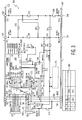
- According to one example embodiment of the present invention, a controllable switch is operated to couple test signals via a selected circuit path, the switch being controlled in response to the test signals being detected at an input node. With this approach, switching for routing test data is automatically effected, without necessarily involving manual switching approaches, such as those involving the use of jumpers.
- In a more particular example embodiment of the present invention, a microcontroller is programmed to automatically monitor test data inputs (TDIs) for testing signals. Upon the detection of a test signal, the microcontroller identifies a particular circuit path to which the test data is to be routed, and controls a switch for routing the test signal between the TDIs and the circuit path. In a more particular implementation, the microcontroller is further programmed to control a switch for routing a response to the test signal to a test data output (TDO).
- In another example embodiment of the present invention, an inter-connectable circuit board includes a plurality of circuit paths and controllable switches adapted for routing test data between at least of the circuit paths and a communications node. A microcontroller is programmed for controlling the controllable switches in response to signals monitored at the communications node. In response to detecting a test signal at the communications node, the microcontroller is programmed for identifying a particular one of the circuit paths to which the test signal is to be routed. The microcontroller then controls the controllable switches to couple a signal path between the communications node and the circuit path. With this approach, access to the inter-connectable circuit board, for example, for connecting jumper lines for switching circuits, is not necessary. This approach has also been found useful when the inter-connectable circuit board is connected to another arrangement such that physical access to the inter-connectable circuit board is difficult or not possible.
- In another example embodiment, one or more of the circuit paths discussed in the above paragraph include paths for routing test data between the inter-connectable circuit board and another inter-connectable circuit board. The microcontroller detects the presence of the other inter-connectable circuit board in response to the monitored signals and controls the controllable switches for routing data to and from the other inter-connectable circuit board.
- The above summary of the present invention is not intended to describe each embodiment or every implementation of the present invention. The above summary of the present invention is not intended to describe each illustrated embodiment or every implementation of the present invention. The figures and detailed description that follow more particularly exemplify these embodiments.
Claims (12)
- A microcomputer arrangement (200) communicatively coupled to JTAG test nodes (210), the microcomputer arrangement comprising:a controllable switch arrangement (220) communicatively coupled between the JTAG test nodes and at least two JTAG signal paths (240, 246); anda microcontroller (205) communicatively coupled to the JTAG test nodes and programmed to control the controllable switch arrangement to route data between at least one of the JTAG test nodes and at least one of the JTAG signal paths, characterized in that the microcontroller is:arranged to monitor the JTAG test nodes to automatically detect a test signal at one of the JTAG test nodes; andprogrammed to control the controllable switch arrangement in response to the automatically detected test signal.
- The microcomputer arrangement of claim 1, wherein the microcontroller is programmed for controlling the controllable switch arrangement to route data between the JTAG test nodes and a particular device along one of the JTAG signal paths for performing a JTAG test on the particular device.
- The microcomputer arrangement of claim 1, wherein the microcontroller is programmed to monitor the JTAG test nodes using an interrupt routine for automatically detecting the test signal.
- The microcomputer arrangement of claim 3, wherein the microcontroller is programmed to monitor the JTAG test nodes using a plurality of interrupt routines, each of the plurality of interrupt routines being adapted for monitoring one of the JTAG test nodes for detecting a test signal thereon, the microcontroller being adapted for routing the data between the monitored JTAG test node and at least one of the JTAG signal paths in response to the interrupt routine detecting a test signal on the monitored JTAG test node.
- The microcomputer arrangement of claim 4, wherein each interrupt routine is assigned to a single JTAG test node and wherein the microcontroller is programmed to control the controllable switch to route data between a particular JTAG test node and one of the JTAG signal paths as a function of the assignment of the particular interrupt routine that detects a test signal.
- The microcomputer arrangement of claim 1, wherein the controllable switch arrangement is adapted to route data along a JTAG signal path from a first JTAG test node to a second JTAG test node in response to the microcontroller.
- The microcomputer arrangement of claim 1, wherein the controllable switch arrangement is adapted to route data along a JTAG signal path from a first JTAG test node to a device that responds to the data and to route a response of the device to a JTAG test output node.
- The microcomputer arrangement of claim 7, wherein the device includes at least one of:an FPGA device, an FPGA plug-in board, an expansion board and an external circuit communicatively coupled with the microcontroller.
- The microcomputer arrangement of claim 1, further comprising an inter-connectable circuit board configured and arranged for connecting to other inter-connectable circuit boards, wherein the controllable switch arrangement and the at least two JTAG signal paths are disposed on the inter-connectable circuit board.
- The microcomputer arrangement of claim 9, wherein the inter-connectable circuit board is configured and arranged for coupling with another inter-connectable circuit board such that physical access to the controllable switch arrangement is prevented.
- The microcomputer arrangement of claim 10, wherein the controllable switch arrangement is adapted for routing the data along a JTAG signal path that includes a signal path between the inter-connectable circuit board and the other inter-connectable circuit board.
- A system for designing a semiconductor device, the system comprising:a deconfigurable and extendible reference-chip development platform that is programmable, and includes a hardware reconfigurable circuit (300) and a plurality of functional block macros, the hardware reconfigurable circuit comprising:a microcomputer arrangement as claimed in claim 1;a collection of functional block macros, at least one of which is obtained from the deconfigurable and extendible reference-chip development platform;an interface circuit configured and arranged to extend the deconfigurable and extendible reference-chip development platform, including a two-way buffer arrangement and logic circuitry adapted to communicatively couple a plurality of external devices with the reference-chip development platform, and therein provide an extended deconfigurable and extendible reference chip development platform that enables co-development and co-validation of hardware and software;a synthesizer adapted to cause said at least one of the functional block macros to be represented as a configuration of the hardware reconfigurable circuit; andwherein the extended deconfigurable and extendible reference-chip development platform is adapted to validate the configuration in the hardware reconfigurable circuit within the extended deconfigurable and extendible reference-chip development platform.
Applications Claiming Priority (3)
| Application Number | Priority Date | Filing Date | Title |
|---|---|---|---|
| US45209503P | 2003-03-04 | 2003-03-04 | |
| US452095P | 2003-03-04 | ||
| PCT/IB2004/000528 WO2004079382A1 (en) | 2003-03-04 | 2004-02-28 | Automatically detecting and routing of test signals |
Publications (2)
| Publication Number | Publication Date |
|---|---|
| EP1601984A1 EP1601984A1 (en) | 2005-12-07 |
| EP1601984B1 true EP1601984B1 (en) | 2007-08-15 |
Family
ID=32962688
Family Applications (1)
| Application Number | Title | Priority Date | Filing Date |
|---|---|---|---|
| EP04715833A Expired - Lifetime EP1601984B1 (en) | 2003-03-04 | 2004-02-28 | Automatically detecting and routing of test signals |
Country Status (7)
| Country | Link |
|---|---|
| US (1) | US20060200715A1 (en) |
| EP (1) | EP1601984B1 (en) |
| JP (1) | JP2006519388A (en) |
| CN (1) | CN1756962A (en) |
| AT (1) | ATE370424T1 (en) |
| DE (1) | DE602004008234T2 (en) |
| WO (1) | WO2004079382A1 (en) |
Families Citing this family (8)
| Publication number | Priority date | Publication date | Assignee | Title |
|---|---|---|---|---|
| US6839242B2 (en) * | 2003-02-13 | 2005-01-04 | Rincon Research Corporation | Reconfigurable circuit modules |
| US20050149783A1 (en) * | 2003-12-11 | 2005-07-07 | International Business Machines Corporation | Methods and apparatus for testing an IC |
| US7464314B2 (en) * | 2005-05-12 | 2008-12-09 | Realtek Semiconductor Corp. | Method for validating an integrated circuit and related semiconductor product thereof |
| FR2879297A1 (en) * | 2005-05-31 | 2006-06-16 | France Telecom | Electronic component e.g. field programmable gate array, programming and testing system, has switches to isolate bus of daughterboard from daughterboard and motherboard connection units when component control device is connected to bus |
| JP5067266B2 (en) | 2008-06-04 | 2012-11-07 | 富士通株式会社 | Integrated circuit board with JTAG function |
| CN101871995B (en) * | 2009-04-23 | 2013-01-02 | 华为技术有限公司 | JTAG (Joint Test Action Group) connection control device and veneer |
| CN102353867A (en) * | 2011-06-08 | 2012-02-15 | 伟创力电子技术(苏州)有限公司 | Interconnection test equipment and method |
| CN110174531B (en) * | 2019-05-24 | 2021-08-03 | 成都飞机工业(集团)有限责任公司 | Reconfigurable interface circuit for signal path of airplane/suspended object test system |
Family Cites Families (7)
| Publication number | Priority date | Publication date | Assignee | Title |
|---|---|---|---|---|
| US5636227A (en) * | 1994-07-08 | 1997-06-03 | Advanced Risc Machines Limited | Integrated circuit test mechansim and method |
| US6408413B1 (en) * | 1998-02-18 | 2002-06-18 | Texas Instruments Incorporated | Hierarchical access of test access ports in embedded core integrated circuits |
| JP2001201543A (en) * | 2000-01-18 | 2001-07-27 | Rooran:Kk | Recording medium with scan pass constructing program recorded thereon, constructing method of scan pass, and arithmetic processing system with this scan pass integrated therein |
| JP3980827B2 (en) * | 2000-03-10 | 2007-09-26 | 株式会社ルネサステクノロジ | Semiconductor integrated circuit device and manufacturing method |
| US6785854B1 (en) * | 2000-10-02 | 2004-08-31 | Koninklijke Philips Electronics N.V. | Test access port (TAP) controller system and method to debug internal intermediate scan test faults |
| EP1286279A1 (en) * | 2001-08-21 | 2003-02-26 | Alcatel | Configuration tool |
| US7047457B1 (en) * | 2003-09-11 | 2006-05-16 | Xilinx, Inc. | Testing of a multi-gigabit transceiver |
-
2004
- 2004-02-28 AT AT04715833T patent/ATE370424T1/en not_active IP Right Cessation
- 2004-02-28 CN CNA2004800058609A patent/CN1756962A/en active Pending
- 2004-02-28 JP JP2006506269A patent/JP2006519388A/en not_active Withdrawn
- 2004-02-28 WO PCT/IB2004/000528 patent/WO2004079382A1/en not_active Ceased
- 2004-02-28 EP EP04715833A patent/EP1601984B1/en not_active Expired - Lifetime
- 2004-02-28 US US10/548,993 patent/US20060200715A1/en not_active Abandoned
- 2004-02-28 DE DE602004008234T patent/DE602004008234T2/en not_active Expired - Fee Related
Non-Patent Citations (1)
| Title |
|---|
| None * |
Also Published As
| Publication number | Publication date |
|---|---|
| DE602004008234T2 (en) | 2008-05-08 |
| WO2004079382A1 (en) | 2004-09-16 |
| JP2006519388A (en) | 2006-08-24 |
| CN1756962A (en) | 2006-04-05 |
| ATE370424T1 (en) | 2007-09-15 |
| DE602004008234D1 (en) | 2007-09-27 |
| US20060200715A1 (en) | 2006-09-07 |
| EP1601984A1 (en) | 2005-12-07 |
Similar Documents
| Publication | Publication Date | Title |
|---|---|---|
| US6886121B2 (en) | Hierarchical test circuit structure for chips with multiple circuit blocks | |
| US6631504B2 (en) | Hierarchical test circuit structure for chips with multiple circuit blocks | |
| US7181705B2 (en) | Hierarchical test circuit structure for chips with multiple circuit blocks | |
| US20200064405A1 (en) | Combinatorial serial and parallel test access port selection in a jtag interface | |
| US7058868B2 (en) | Scan testing mode control of gated clock signals for memory devices | |
| US8566656B2 (en) | Testing circuit and method | |
| US7219278B2 (en) | Configurator arrangement and approach therefor | |
| US20060200715A1 (en) | Automatically detecting and routing of test signals | |
| EP1236053B1 (en) | A test access port (tap) controller system and method to debug internal intermediate scan test faults | |
| US6308292B1 (en) | File driven mask insertion for automatic test equipment test pattern generation | |
| US6973631B2 (en) | Scan insertion with bypass login in an IC design | |
| US20040193979A1 (en) | Circuit configurator arrangement and approach therefor | |
| US20070079200A1 (en) | Input-output device testing | |
| CN114781304A (en) | Method and system for controlling pin state of chip, chip and upper computer | |
| US7089471B2 (en) | Scan testing mode control of gated clock signals for flip-flops | |
| US20040123206A1 (en) | System and method for evaluating an integrated circuit design | |
| KR100622143B1 (en) | Multiplexing Device of I / O Port | |
| JP3094983B2 (en) | System logic test circuit and test method | |
| CN1965242A (en) | Test method and test device for testing an integrated circuit | |
| US20020186585A1 (en) | Semiconductor integrated circuit device and method for designing a semiconductor integrated circuit device | |
| KR200221586Y1 (en) | Electronic equipment checking device | |
| WO2008050505A1 (en) | Simulation apparatus | |
| Renaudin et al. | A 6-Wire Plug and Play Clockless Distributed On-Chip-Sensor Network in 28 nm UTBB FD-SOI | |
| JPH02112777A (en) | Semiconductor integrated circuit | |
| Zivkovic et al. | Core-Based Testing of Embedded Mixed-Signal Modules in a SoC |
Legal Events
| Date | Code | Title | Description |
|---|---|---|---|
| PUAI | Public reference made under article 153(3) epc to a published international application that has entered the european phase |
Free format text: ORIGINAL CODE: 0009012 |
|
| 17P | Request for examination filed |
Effective date: 20051004 |
|
| AK | Designated contracting states |
Kind code of ref document: A1 Designated state(s): AT BE BG CH CY CZ DE DK EE ES FI FR GB GR HU IE IT LI LU MC NL PT RO SE SI SK TR |
|
| AX | Request for extension of the european patent |
Extension state: AL LT LV MK |
|
| DAX | Request for extension of the european patent (deleted) | ||
| GRAP | Despatch of communication of intention to grant a patent |
Free format text: ORIGINAL CODE: EPIDOSNIGR1 |
|
| GRAS | Grant fee paid |
Free format text: ORIGINAL CODE: EPIDOSNIGR3 |
|
| GRAA | (expected) grant |
Free format text: ORIGINAL CODE: 0009210 |
|
| AK | Designated contracting states |
Kind code of ref document: B1 Designated state(s): AT BE BG CH CY CZ DE DK EE ES FI FR GB GR HU IE IT LI LU MC NL PT RO SE SI SK TR |
|
| REG | Reference to a national code |
Ref country code: GB Ref legal event code: FG4D |
|
| REG | Reference to a national code |
Ref country code: CH Ref legal event code: EP |
|
| REG | Reference to a national code |
Ref country code: IE Ref legal event code: FG4D |
|
| REF | Corresponds to: |
Ref document number: 602004008234 Country of ref document: DE Date of ref document: 20070927 Kind code of ref document: P |
|
| PG25 | Lapsed in a contracting state [announced via postgrant information from national office to epo] |
Ref country code: ES Free format text: LAPSE BECAUSE OF FAILURE TO SUBMIT A TRANSLATION OF THE DESCRIPTION OR TO PAY THE FEE WITHIN THE PRESCRIBED TIME-LIMIT Effective date: 20071126 Ref country code: BG Free format text: LAPSE BECAUSE OF FAILURE TO SUBMIT A TRANSLATION OF THE DESCRIPTION OR TO PAY THE FEE WITHIN THE PRESCRIBED TIME-LIMIT Effective date: 20071115 Ref country code: NL Free format text: LAPSE BECAUSE OF FAILURE TO SUBMIT A TRANSLATION OF THE DESCRIPTION OR TO PAY THE FEE WITHIN THE PRESCRIBED TIME-LIMIT Effective date: 20070815 Ref country code: FI Free format text: LAPSE BECAUSE OF FAILURE TO SUBMIT A TRANSLATION OF THE DESCRIPTION OR TO PAY THE FEE WITHIN THE PRESCRIBED TIME-LIMIT Effective date: 20070815 |
|
| NLV1 | Nl: lapsed or annulled due to failure to fulfill the requirements of art. 29p and 29m of the patents act | ||
| PG25 | Lapsed in a contracting state [announced via postgrant information from national office to epo] |
Ref country code: LI Free format text: LAPSE BECAUSE OF FAILURE TO SUBMIT A TRANSLATION OF THE DESCRIPTION OR TO PAY THE FEE WITHIN THE PRESCRIBED TIME-LIMIT Effective date: 20070815 Ref country code: AT Free format text: LAPSE BECAUSE OF FAILURE TO SUBMIT A TRANSLATION OF THE DESCRIPTION OR TO PAY THE FEE WITHIN THE PRESCRIBED TIME-LIMIT Effective date: 20070815 Ref country code: CH Free format text: LAPSE BECAUSE OF FAILURE TO SUBMIT A TRANSLATION OF THE DESCRIPTION OR TO PAY THE FEE WITHIN THE PRESCRIBED TIME-LIMIT Effective date: 20070815 |
|
| REG | Reference to a national code |
Ref country code: CH Ref legal event code: PL |
|
| ET | Fr: translation filed | ||
| PG25 | Lapsed in a contracting state [announced via postgrant information from national office to epo] |
Ref country code: BE Free format text: LAPSE BECAUSE OF FAILURE TO SUBMIT A TRANSLATION OF THE DESCRIPTION OR TO PAY THE FEE WITHIN THE PRESCRIBED TIME-LIMIT Effective date: 20070815 |
|
| PG25 | Lapsed in a contracting state [announced via postgrant information from national office to epo] |
Ref country code: GR Free format text: LAPSE BECAUSE OF FAILURE TO SUBMIT A TRANSLATION OF THE DESCRIPTION OR TO PAY THE FEE WITHIN THE PRESCRIBED TIME-LIMIT Effective date: 20071116 Ref country code: DK Free format text: LAPSE BECAUSE OF FAILURE TO SUBMIT A TRANSLATION OF THE DESCRIPTION OR TO PAY THE FEE WITHIN THE PRESCRIBED TIME-LIMIT Effective date: 20070815 |
|
| PG25 | Lapsed in a contracting state [announced via postgrant information from national office to epo] |
Ref country code: CZ Free format text: LAPSE BECAUSE OF FAILURE TO SUBMIT A TRANSLATION OF THE DESCRIPTION OR TO PAY THE FEE WITHIN THE PRESCRIBED TIME-LIMIT Effective date: 20070815 Ref country code: SK Free format text: LAPSE BECAUSE OF FAILURE TO SUBMIT A TRANSLATION OF THE DESCRIPTION OR TO PAY THE FEE WITHIN THE PRESCRIBED TIME-LIMIT Effective date: 20070815 Ref country code: PT Free format text: LAPSE BECAUSE OF FAILURE TO SUBMIT A TRANSLATION OF THE DESCRIPTION OR TO PAY THE FEE WITHIN THE PRESCRIBED TIME-LIMIT Effective date: 20080115 |
|
| PGFP | Annual fee paid to national office [announced via postgrant information from national office to epo] |
Ref country code: GB Payment date: 20080327 Year of fee payment: 5 |
|
| PLBE | No opposition filed within time limit |
Free format text: ORIGINAL CODE: 0009261 |
|
| STAA | Information on the status of an ep patent application or granted ep patent |
Free format text: STATUS: NO OPPOSITION FILED WITHIN TIME LIMIT |
|
| PG25 | Lapsed in a contracting state [announced via postgrant information from national office to epo] |
Ref country code: SE Free format text: LAPSE BECAUSE OF FAILURE TO SUBMIT A TRANSLATION OF THE DESCRIPTION OR TO PAY THE FEE WITHIN THE PRESCRIBED TIME-LIMIT Effective date: 20071115 Ref country code: RO Free format text: LAPSE BECAUSE OF FAILURE TO SUBMIT A TRANSLATION OF THE DESCRIPTION OR TO PAY THE FEE WITHIN THE PRESCRIBED TIME-LIMIT Effective date: 20070815 |
|
| 26N | No opposition filed |
Effective date: 20080516 |
|
| PGFP | Annual fee paid to national office [announced via postgrant information from national office to epo] |
Ref country code: FR Payment date: 20080227 Year of fee payment: 5 Ref country code: DE Payment date: 20080415 Year of fee payment: 5 |
|
| PG25 | Lapsed in a contracting state [announced via postgrant information from national office to epo] |
Ref country code: MC Free format text: LAPSE BECAUSE OF NON-PAYMENT OF DUE FEES Effective date: 20080228 |
|
| PG25 | Lapsed in a contracting state [announced via postgrant information from national office to epo] |
Ref country code: EE Free format text: LAPSE BECAUSE OF FAILURE TO SUBMIT A TRANSLATION OF THE DESCRIPTION OR TO PAY THE FEE WITHIN THE PRESCRIBED TIME-LIMIT Effective date: 20070815 Ref country code: IE Free format text: LAPSE BECAUSE OF NON-PAYMENT OF DUE FEES Effective date: 20080228 |
|
| PG25 | Lapsed in a contracting state [announced via postgrant information from national office to epo] |
Ref country code: SI Free format text: LAPSE BECAUSE OF FAILURE TO SUBMIT A TRANSLATION OF THE DESCRIPTION OR TO PAY THE FEE WITHIN THE PRESCRIBED TIME-LIMIT Effective date: 20070815 |
|
| PG25 | Lapsed in a contracting state [announced via postgrant information from national office to epo] |
Ref country code: CY Free format text: LAPSE BECAUSE OF FAILURE TO SUBMIT A TRANSLATION OF THE DESCRIPTION OR TO PAY THE FEE WITHIN THE PRESCRIBED TIME-LIMIT Effective date: 20070815 |
|
| GBPC | Gb: european patent ceased through non-payment of renewal fee |
Effective date: 20090228 |
|
| REG | Reference to a national code |
Ref country code: FR Ref legal event code: ST Effective date: 20091030 |
|
| PG25 | Lapsed in a contracting state [announced via postgrant information from national office to epo] |
Ref country code: DE Free format text: LAPSE BECAUSE OF NON-PAYMENT OF DUE FEES Effective date: 20090901 |
|
| PG25 | Lapsed in a contracting state [announced via postgrant information from national office to epo] |
Ref country code: FR Free format text: LAPSE BECAUSE OF NON-PAYMENT OF DUE FEES Effective date: 20090302 Ref country code: GB Free format text: LAPSE BECAUSE OF NON-PAYMENT OF DUE FEES Effective date: 20090228 |
|
| PG25 | Lapsed in a contracting state [announced via postgrant information from national office to epo] |
Ref country code: LU Free format text: LAPSE BECAUSE OF NON-PAYMENT OF DUE FEES Effective date: 20080228 Ref country code: HU Free format text: LAPSE BECAUSE OF FAILURE TO SUBMIT A TRANSLATION OF THE DESCRIPTION OR TO PAY THE FEE WITHIN THE PRESCRIBED TIME-LIMIT Effective date: 20080216 |
|
| PG25 | Lapsed in a contracting state [announced via postgrant information from national office to epo] |
Ref country code: TR Free format text: LAPSE BECAUSE OF FAILURE TO SUBMIT A TRANSLATION OF THE DESCRIPTION OR TO PAY THE FEE WITHIN THE PRESCRIBED TIME-LIMIT Effective date: 20070815 |
|
| PG25 | Lapsed in a contracting state [announced via postgrant information from national office to epo] |
Ref country code: IT Free format text: LAPSE BECAUSE OF NON-PAYMENT OF DUE FEES Effective date: 20080229 |