EP1601103A1 - Phase comparison circuit and cdr circuit - Google Patents
Phase comparison circuit and cdr circuit Download PDFInfo
- Publication number
- EP1601103A1 EP1601103A1 EP04717309A EP04717309A EP1601103A1 EP 1601103 A1 EP1601103 A1 EP 1601103A1 EP 04717309 A EP04717309 A EP 04717309A EP 04717309 A EP04717309 A EP 04717309A EP 1601103 A1 EP1601103 A1 EP 1601103A1
- Authority
- EP
- European Patent Office
- Prior art keywords
- signal
- circuit
- phase
- clock signal
- phase error
- Prior art date
- Legal status (The legal status is an assumption and is not a legal conclusion. Google has not performed a legal analysis and makes no representation as to the accuracy of the status listed.)
- Granted
Links
Images



Classifications
-
- H—ELECTRICITY
- H03—ELECTRONIC CIRCUITRY
- H03L—AUTOMATIC CONTROL, STARTING, SYNCHRONISATION OR STABILISATION OF GENERATORS OF ELECTRONIC OSCILLATIONS OR PULSES
- H03L7/00—Automatic control of frequency or phase; Synchronisation
- H03L7/06—Automatic control of frequency or phase; Synchronisation using a reference signal applied to a frequency- or phase-locked loop
- H03L7/08—Details of the phase-locked loop
- H03L7/085—Details of the phase-locked loop concerning mainly the frequency- or phase-detection arrangement including the filtering or amplification of its output signal
- H03L7/089—Details of the phase-locked loop concerning mainly the frequency- or phase-detection arrangement including the filtering or amplification of its output signal the phase or frequency detector generating up-down pulses
- H03L7/0891—Details of the phase-locked loop concerning mainly the frequency- or phase-detection arrangement including the filtering or amplification of its output signal the phase or frequency detector generating up-down pulses the up-down pulses controlling source and sink current generators, e.g. a charge pump
- H03L7/0893—Details of the phase-locked loop concerning mainly the frequency- or phase-detection arrangement including the filtering or amplification of its output signal the phase or frequency detector generating up-down pulses the up-down pulses controlling source and sink current generators, e.g. a charge pump the up-down pulses controlling at least two source current generators or at least two sink current generators connected to different points in the loop
-
- H—ELECTRICITY
- H03—ELECTRONIC CIRCUITRY
- H03L—AUTOMATIC CONTROL, STARTING, SYNCHRONISATION OR STABILISATION OF GENERATORS OF ELECTRONIC OSCILLATIONS OR PULSES
- H03L7/00—Automatic control of frequency or phase; Synchronisation
- H03L7/06—Automatic control of frequency or phase; Synchronisation using a reference signal applied to a frequency- or phase-locked loop
- H03L7/08—Details of the phase-locked loop
- H03L7/085—Details of the phase-locked loop concerning mainly the frequency- or phase-detection arrangement including the filtering or amplification of its output signal
- H03L7/089—Details of the phase-locked loop concerning mainly the frequency- or phase-detection arrangement including the filtering or amplification of its output signal the phase or frequency detector generating up-down pulses
- H03L7/0891—Details of the phase-locked loop concerning mainly the frequency- or phase-detection arrangement including the filtering or amplification of its output signal the phase or frequency detector generating up-down pulses the up-down pulses controlling source and sink current generators, e.g. a charge pump
- H03L7/0895—Details of the current generators
-
- H—ELECTRICITY
- H03—ELECTRONIC CIRCUITRY
- H03L—AUTOMATIC CONTROL, STARTING, SYNCHRONISATION OR STABILISATION OF GENERATORS OF ELECTRONIC OSCILLATIONS OR PULSES
- H03L7/00—Automatic control of frequency or phase; Synchronisation
- H03L7/06—Automatic control of frequency or phase; Synchronisation using a reference signal applied to a frequency- or phase-locked loop
- H03L7/08—Details of the phase-locked loop
- H03L7/085—Details of the phase-locked loop concerning mainly the frequency- or phase-detection arrangement including the filtering or amplification of its output signal
- H03L7/091—Details of the phase-locked loop concerning mainly the frequency- or phase-detection arrangement including the filtering or amplification of its output signal the phase or frequency detector using a sampling device
-
- H—ELECTRICITY
- H04—ELECTRIC COMMUNICATION TECHNIQUE
- H04L—TRANSMISSION OF DIGITAL INFORMATION, e.g. TELEGRAPHIC COMMUNICATION
- H04L7/00—Arrangements for synchronising receiver with transmitter
- H04L7/02—Speed or phase control by the received code signals, the signals containing no special synchronisation information
- H04L7/033—Speed or phase control by the received code signals, the signals containing no special synchronisation information using the transitions of the received signal to control the phase of the synchronising-signal-generating means, e.g. using a phase-locked loop
Definitions
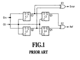
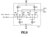
- the output of the exclusive OR circuit E1 is the phase error signal Error 1 (the first phase error signal) to the phase comparator circuit.
- the output of the exclusive OR circuit E2 is the phase error signal Error 2 (the second phase error signal) to the phase comparator circuit.
Landscapes
- Engineering & Computer Science (AREA)
- Computer Networks & Wireless Communication (AREA)
- Signal Processing (AREA)
- Manipulation Of Pulses (AREA)
- Stabilization Of Oscillater, Synchronisation, Frequency Synthesizers (AREA)
Abstract
Description
Claims (8)
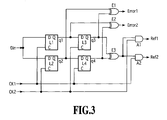
- A phase comparator circuit for operating with a clock signal whose period is 2 times the unit time width of an inputted data signal, said phase comparator circuit characterized in that;
said data signal is inputted to a first latch circuit and a second latch circuit, said first latch circuit performs the latching operation thereof with a first clock signal, and said second latching circuit performs the latching operation thereof with the second clock signal, as being an inverted clock signal of said first clock signal;
the output of said first latching circuit is inputted to a third latch circuit, the output of said second latch circuit is inputted to a fourth latch circuit, said third latch circuit performs the latching operation thereof with said second clock signal, and said fourth latch circuit performs the latching operation thereof with said first clock signal; and
an exclusive OR of the output from said second latch circuit and the output from said third latch circuit is used as a first phase error signal, and an exclusive OR of the output from said first latch circuit and the output from said fourth latch circuit is used as second phase error signal. - The phase comparator circuit as defined in claim 1, characterized in that the output of said second latch circuit is connected to a first delay circuit, an exclusive OR of the output from the first delay circuit and the output from said third latch circuit is used as said first phase error signal; and
the output of said first latch circuit is connected to the second delay circuit, an exclusive OR of said second delay circuit and the output of said fourth latch circuit is used as said second phase error signal. - A phase comparator circuit for operating with a clock signal whose period is 2 times the unit time width of an inputted data signal, said phase comparator circuit characterized in that;
a first phase error signal, representing the phase difference between the transition point of said data signal and the rising edge of a first clock signal as the pulse width, is outputted; and
a second phase error signal, representing the phase difference between the transition point of said data signal and the rising edge of a second clock signal as being the inverted clock signal of said first clock signal, is outputted. - The phase comparator circuit as defined in claim 3, characterized in that, when the transition has occurred between 2 consecutive data in said data signal, a first reference signal, having a time width ranging from the rising edge of said second clock signal to the rising edge of said first clock signal, is outputted in order to determine the increase or the decrease of the pulse width of said first phase error signal; and
when the transition has occurred between 2 consecutive data in said data signal, a second reference signal, having a time width ranging from the rising edge of said first clock signal to the rising edge of said second clock signal, is outputted in order to determine the increase or decrease of the pulse width of said second phase error signal. - A phase comparator circuit for operating with a clock signal whose period is 2 times the unit time width of an inputted data signal, said phase comparator circuit characterized in that;
the pulse width of the phase error signal representing the phase difference between the transition point of said data signal and the transition point of said clock signal is extended by the time width corresponding to the unit time width of said data signal. - The phase comparator circuit as def ined in claim 5, characterized in that the first phase error signal, representing the pulse width as being the phase difference between the transition point of the data signal of the even-number sequential order and the rising edge of the said clock signal, is outputted; and
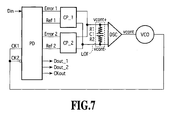
the second phase error signal, representing the pulse width as being the phase difference between the transition point of the said data signal of odd-number sequential order and the falling edge of said clock signal, is outputted. - A CDR circuit including a phase comparator circuit, a charge pump circuit and a loop filter, operating with a clock signal whose period is 2 times the unit time width of an inputted data signal, and
characterized in that;
said phase comparator circuit outputs a first phase error signal, representing the pulse width as being the phase difference between the transition point of the said data signal and the rising edge of said clock signal, and a second phase error signal, representing the pulse width as being the phase difference between the transition point of said data signal and the falling edge of said clock signal;
when the transition has occurred between two consecutive data in said data signal, said phase comparator circuit outputs a first reference signal, having a time width ranging from the falling edge of said clock signal to the rising edge of said clock signal, and a second reference signal, having a time width ranging from the rising edge of said clock signal to the falling edge of said clock signal;
said charge pump circuit comprises a first charge pump circuit for receiving the input of said first phase error signal and the input of said reference signal, and a second charge pump circuit for receiving the input of said second phase error signal and said second reference signal; and
the source current to flow into said loop filter according to the said first and second phase error signals and the sink current to flow into said loop filter according to said first and second reference signals are designed to become equal with each other when the phase of said data signal and the phase of said clock signal coincide with each other. - The CDR circuit as defined in claim 7,
characterized in that said charge pump circuit includes a current supply means to be controlled by external voltage so as to adjust the ratio between said source current and said sink current.
Applications Claiming Priority (5)
| Application Number | Priority Date | Filing Date | Title |
|---|---|---|---|
| JP2003057261 | 2003-03-04 | ||
| JP2003057261 | 2003-03-04 | ||
| JP2003073720 | 2003-03-18 | ||
| JP2003073720 | 2003-03-18 | ||
| PCT/JP2004/002714 WO2004079907A1 (en) | 2003-03-04 | 2004-03-04 | Phase comparison circuit and cdr circuit |
Publications (3)
| Publication Number | Publication Date |
|---|---|
| EP1601103A1 true EP1601103A1 (en) | 2005-11-30 |
| EP1601103A4 EP1601103A4 (en) | 2006-05-17 |
| EP1601103B1 EP1601103B1 (en) | 2012-02-29 |
Family
ID=32964884
Family Applications (1)
| Application Number | Title | Priority Date | Filing Date |
|---|---|---|---|
| EP04717309A Expired - Lifetime EP1601103B1 (en) | 2003-03-04 | 2004-03-04 | Phase comparison circuit and cdr circuit |
Country Status (4)
| Country | Link |
|---|---|
| US (1) | US7368954B2 (en) |
| EP (1) | EP1601103B1 (en) |
| JP (1) | JP3955076B2 (en) |
| WO (1) | WO2004079907A1 (en) |
Cited By (1)
| Publication number | Priority date | Publication date | Assignee | Title |
|---|---|---|---|---|
| US11777701B2 (en) * | 2018-07-10 | 2023-10-03 | Socionext Inc. | Phase synchronization circuit, transmission and reception circuit, and integrated circuit |
Families Citing this family (7)
| Publication number | Priority date | Publication date | Assignee | Title |
|---|---|---|---|---|
| KR101025234B1 (en) * | 2003-02-28 | 2011-04-01 | 오스람 옵토 세미컨덕터스 게엠베하 | An optoelectronic device having a housing body metallized in a structured manner, a method of manufacturing the optoelectronic device and a method for metallizing a housing body including plastic in a structured manner. |
| US7433442B2 (en) * | 2004-09-23 | 2008-10-07 | Standard Microsystems Corporation | Linear half-rate clock and data recovery (CDR) circuit |
| TWI270783B (en) * | 2005-02-24 | 2007-01-11 | Via Tech Inc | Method and circuitry for extracting clock in clock data recovery system |
| JP2009231896A (en) * | 2008-03-19 | 2009-10-08 | Fujitsu Ltd | Receiving device and receiving method |
| US8299826B2 (en) * | 2009-08-25 | 2012-10-30 | Sitime Corporation | Phase locked loop circuitry having switched resistor loop filter circuitry, and methods of operating same |
| JP2011061350A (en) * | 2009-09-08 | 2011-03-24 | Renesas Electronics Corp | Receiving apparatus and receiving method thereof |
| JP2011120106A (en) * | 2009-12-04 | 2011-06-16 | Rohm Co Ltd | Clock data recovery circuit |
Family Cites Families (14)
| Publication number | Priority date | Publication date | Assignee | Title |
|---|---|---|---|---|
| GB2089601A (en) * | 1980-12-12 | 1982-06-23 | Philips Electronic Associated | Phase Sensitive Detector |
| WO1992007425A1 (en) * | 1990-10-23 | 1992-04-30 | Seiko Epson Corporation | Voltage-controlled oscillating circuit and phase-locked loop |
| US5220275A (en) * | 1991-07-26 | 1993-06-15 | Ericsson Ge Mobile Communication Holding, Inc. | Accumulator phase digitizer |
| US5428648A (en) * | 1992-09-18 | 1995-06-27 | Sony Corporation | Digital PLL circuit having signal edge position measurement |
| JP3094971B2 (en) | 1997-10-08 | 2000-10-03 | 日本電気株式会社 | Phase comparison circuit, phase-locked loop circuit and serial-parallel conversion circuit using the same |
| JP3196725B2 (en) | 1998-06-09 | 2001-08-06 | 日本電気株式会社 | Phase comparison circuit |
| JP3463575B2 (en) | 1998-09-03 | 2003-11-05 | 日本ビクター株式会社 | Digital phase comparator |
| US6072337A (en) | 1998-12-18 | 2000-06-06 | Cypress Semiconductor Corp. | Phase detector |
| JP3864644B2 (en) | 1999-11-15 | 2007-01-10 | 富士通株式会社 | Phase comparison circuit with lock detection function |
| JP2001196907A (en) | 2000-01-13 | 2001-07-19 | Nec Eng Ltd | Phase comparator circuit |
| US6771728B1 (en) * | 2000-09-20 | 2004-08-03 | Applied Micro Circuits Corporation | Half-rate phase detector with reduced timing requirements |
| JP2002171160A (en) | 2000-12-01 | 2002-06-14 | Nec Eng Ltd | Phase comparing circuit |
| JP3770378B2 (en) | 2001-04-16 | 2006-04-26 | 日本電信電話株式会社 | Phase comparison circuit |
| JP4007814B2 (en) | 2002-01-28 | 2007-11-14 | 三菱電機株式会社 | Half-rate CDR circuit |
-
2004
- 2004-03-04 JP JP2005503089A patent/JP3955076B2/en not_active Expired - Fee Related
- 2004-03-04 EP EP04717309A patent/EP1601103B1/en not_active Expired - Lifetime
- 2004-03-04 US US10/535,273 patent/US7368954B2/en not_active Expired - Fee Related
- 2004-03-04 WO PCT/JP2004/002714 patent/WO2004079907A1/en not_active Ceased
Cited By (1)
| Publication number | Priority date | Publication date | Assignee | Title |
|---|---|---|---|---|
| US11777701B2 (en) * | 2018-07-10 | 2023-10-03 | Socionext Inc. | Phase synchronization circuit, transmission and reception circuit, and integrated circuit |
Also Published As
| Publication number | Publication date |
|---|---|
| EP1601103A4 (en) | 2006-05-17 |
| JPWO2004079907A1 (en) | 2006-06-08 |
| US20060050828A1 (en) | 2006-03-09 |
| WO2004079907A1 (en) | 2004-09-16 |
| EP1601103B1 (en) | 2012-02-29 |
| US7368954B2 (en) | 2008-05-06 |
| JP3955076B2 (en) | 2007-08-08 |
Similar Documents
| Publication | Publication Date | Title |
|---|---|---|
| US6252465B1 (en) | Data phase locked loop circuit | |
| US5410263A (en) | Delay line loop for on-chip clock synthesis with zero skew and 50% duty cycle | |
| JP2004104522A (en) | Clock reproducing device, and electronic apparatus using the same | |
| US20050093634A1 (en) | Clock generator and related biasing circuit | |
| Yang | Delay-locked loops-an overview | |
| US6249159B1 (en) | Frequency control circuit having increased control bandwidth at lower device operating speed | |
| JP2011120106A (en) | Clock data recovery circuit | |
| US6320424B1 (en) | Method of providing and circuit for providing phase lock loop frequency overshoot control | |
| JP4484629B2 (en) | Clock data recovery circuit and voltage controlled oscillation circuit | |
| EP1601103B1 (en) | Phase comparison circuit and cdr circuit | |
| JP4751932B2 (en) | Phase detection device and phase synchronization device | |
| US7983361B2 (en) | Clock data recovery circuit | |
| KR101002242B1 (en) | Dual-Rate Clock and Data Recovery Circuits Using Quarter-Rate Linear Phase Detectors | |
| US7855584B2 (en) | Low lock time delay locked loops using time cycle suppressor | |
| US7256635B2 (en) | Low lock time delay locked loops using time cycle suppressor | |
| JP2004356701A (en) | Half rate CDR circuit | |
| CN100346574C (en) | Phase comparison circuit and CDR circuit | |
| US7023944B2 (en) | Method and circuit for glitch-free changing of clocks having different phases | |
| Gimeno et al. | Low-power half-rate dual-loop clock-recovery system in 28-nm FDSOI | |
| Jeon et al. | Area efficient 4Gb/s clock data recovery using improved phase interpolator with error monitor | |
| KR19980019934A (en) | Piel for Clock / Data Recovery Using Multiphase Clock | |
| US20040183570A1 (en) | Phase comparator capable of performing stable phase comparison for high frequency band | |
| Lin | Research and design of low jitter, wide locking-range all-digital phase-locked and delay-locked loops | |
| KR101831228B1 (en) | Multi clock generator | |
| JP5420748B2 (en) | Clock data recovery circuit |
Legal Events
| Date | Code | Title | Description |
|---|---|---|---|
| PUAI | Public reference made under article 153(3) epc to a published international application that has entered the european phase |
Free format text: ORIGINAL CODE: 0009012 |
|
| 17P | Request for examination filed |
Effective date: 20050726 |
|
| AK | Designated contracting states |
Kind code of ref document: A1 Designated state(s): AT BE BG CH CY CZ DE DK EE ES FI FR GB GR HU IE IT LI LU MC NL PL PT RO SE SI SK TR |
|
| AX | Request for extension of the european patent |
Extension state: AL LT LV MK |
|
| A4 | Supplementary search report drawn up and despatched |
Effective date: 20060404 |
|
| RIC1 | Information provided on ipc code assigned before grant |
Ipc: H03L 7/08 20060101ALI20060329BHEP Ipc: H03K 5/26 20060101AFI20040922BHEP Ipc: H03L 7/091 20060101ALI20060329BHEP Ipc: H04L 7/033 20060101ALI20060329BHEP |
|
| DAX | Request for extension of the european patent (deleted) | ||
| RBV | Designated contracting states (corrected) |
Designated state(s): DE FR GB |
|
| 17Q | First examination report despatched |
Effective date: 20100218 |
|
| GRAP | Despatch of communication of intention to grant a patent |
Free format text: ORIGINAL CODE: EPIDOSNIGR1 |
|
| GRAS | Grant fee paid |
Free format text: ORIGINAL CODE: EPIDOSNIGR3 |
|
| GRAA | (expected) grant |
Free format text: ORIGINAL CODE: 0009210 |
|
| AK | Designated contracting states |
Kind code of ref document: B1 Designated state(s): DE FR GB |
|
| REG | Reference to a national code |
Ref country code: GB Ref legal event code: FG4D |
|
| REG | Reference to a national code |
Ref country code: DE Ref legal event code: R096 Ref document number: 602004036697 Country of ref document: DE Effective date: 20120426 |
|
| PLBE | No opposition filed within time limit |
Free format text: ORIGINAL CODE: 0009261 |
|
| STAA | Information on the status of an ep patent application or granted ep patent |
Free format text: STATUS: NO OPPOSITION FILED WITHIN TIME LIMIT |
|
| 26N | No opposition filed |
Effective date: 20121130 |
|
| REG | Reference to a national code |
Ref country code: DE Ref legal event code: R097 Ref document number: 602004036697 Country of ref document: DE Effective date: 20121130 |
|
| PGFP | Annual fee paid to national office [announced via postgrant information from national office to epo] |
Ref country code: DE Payment date: 20130322 Year of fee payment: 10 Ref country code: GB Payment date: 20130318 Year of fee payment: 10 Ref country code: FR Payment date: 20130409 Year of fee payment: 10 |
|
| REG | Reference to a national code |
Ref country code: DE Ref legal event code: R119 Ref document number: 602004036697 Country of ref document: DE |
|
| GBPC | Gb: european patent ceased through non-payment of renewal fee |
Effective date: 20140304 |
|
| REG | Reference to a national code |
Ref country code: FR Ref legal event code: ST Effective date: 20141128 |
|
| REG | Reference to a national code |
Ref country code: DE Ref legal event code: R119 Ref document number: 602004036697 Country of ref document: DE Effective date: 20141001 |
|
| PG25 | Lapsed in a contracting state [announced via postgrant information from national office to epo] |
Ref country code: DE Free format text: LAPSE BECAUSE OF NON-PAYMENT OF DUE FEES Effective date: 20141001 Ref country code: FR Free format text: LAPSE BECAUSE OF NON-PAYMENT OF DUE FEES Effective date: 20140331 Ref country code: GB Free format text: LAPSE BECAUSE OF NON-PAYMENT OF DUE FEES Effective date: 20140304 |