EP1598939B1 - Verfahren und Vorrichtung zum dynamischen Phasenabgleich - Google Patents
Verfahren und Vorrichtung zum dynamischen Phasenabgleich Download PDFInfo
- Publication number
- EP1598939B1 EP1598939B1 EP05252993.0A EP05252993A EP1598939B1 EP 1598939 B1 EP1598939 B1 EP 1598939B1 EP 05252993 A EP05252993 A EP 05252993A EP 1598939 B1 EP1598939 B1 EP 1598939B1
- Authority
- EP
- European Patent Office
- Prior art keywords
- phase
- circuitry
- signals
- signal
- transitions
- Prior art date
- Legal status (The legal status is an assumption and is not a legal conclusion. Google has not performed a legal analysis and makes no representation as to the accuracy of the status listed.)
- Expired - Lifetime
Links
Images

Classifications
-
- H—ELECTRICITY
- H03—ELECTRONIC CIRCUITRY
- H03L—AUTOMATIC CONTROL, STARTING, SYNCHRONISATION OR STABILISATION OF GENERATORS OF ELECTRONIC OSCILLATIONS OR PULSES
- H03L7/00—Automatic control of frequency or phase; Synchronisation
- H03L7/06—Automatic control of frequency or phase; Synchronisation using a reference signal applied to a frequency- or phase-locked loop
- H03L7/08—Details of the phase-locked loop
- H03L7/081—Details of the phase-locked loop provided with an additional controlled phase shifter
- H03L7/0812—Details of the phase-locked loop provided with an additional controlled phase shifter and where no voltage or current controlled oscillator is used
- H03L7/0814—Details of the phase-locked loop provided with an additional controlled phase shifter and where no voltage or current controlled oscillator is used the phase shifting device being digitally controlled
-
- H—ELECTRICITY
- H03—ELECTRONIC CIRCUITRY
- H03L—AUTOMATIC CONTROL, STARTING, SYNCHRONISATION OR STABILISATION OF GENERATORS OF ELECTRONIC OSCILLATIONS OR PULSES
- H03L7/00—Automatic control of frequency or phase; Synchronisation
- H03L7/06—Automatic control of frequency or phase; Synchronisation using a reference signal applied to a frequency- or phase-locked loop
- H03L7/08—Details of the phase-locked loop
- H03L7/085—Details of the phase-locked loop concerning mainly the frequency- or phase-detection arrangement including the filtering or amplification of its output signal
- H03L7/087—Details of the phase-locked loop concerning mainly the frequency- or phase-detection arrangement including the filtering or amplification of its output signal using at least two phase detectors or a frequency and phase detector in the loop
Definitions
- This invention relates to methods and apparatus for processing a received serial data signal, and more particularly to methods and apparatus for determining the phase of such a signal so that it can be reliably sampled to recover its data content.
- Receiver circuitry may receive a serial data signal with no accompanying information about the timing of the individual data bits in that signal. This timing information is sometimes referred to as the phase of the signal.
- the receiver circuitry must recover the data from the received signal. To do this, the receiver circuitry needs to sample the received signal during each data bit interval ("unit interval") in that signal to determine whether the signal currently represents a binary 1 or a binary 0.
- Information about the phase of the signal is needed so that the signal can be sampled at a time during each unit interval that will give reliable results. For example, it may be desired to sample the signal as close to the center of each unit interval as possible. Because the data signal is not received with any accompanying phase information, the receiver circuitry itself must derive the phase information it needs from the received data signal.
- the process of determining the phase of a received data signal may be referred to as phase alignment; and because the phase of the received signal may change over time, the phase alignment may need to be dynamic to keep the results current at all times.
- a known dynamic phase alignment (“DPA”) technique includes producing several candidate clock signals, all of which have the same frequency (related to the frequency of the received data signal), and each of which has a unique phase. For example, there may be eight candidate clock signals, the phases of which are equally spaced over one clock signal cycle.
- Phase detector circuitry is used to compare the phase of transitions in the received data signal to the phase of transitions in one of the candidate clock signals. Assuming the phase detector does not detect a perfect phase match (as it almost never does), the phase detector circuitry keeps moving from one candidate clock signal to the next trying to find the candidate signal having the phase that will be best for use in timing the sampling of the data signal.
- phase detector circuitry quickly finds what it regards as currently the best (or at least a very good) candidate clock signal for use in controlling data signal sampling. But continued operation of the phase detector circuitry also typically causes it to switch to a different candidate clock signal as it continues to search for the best such signal to use. The new choice may in fact be somewhat better or somewhat worse than the old choice. In either case, as long as there is still some phase mismatch, the search for the best signal continues, which may cause the phase detector to soon revert to its previous choice. In other words, even when the system is effectively at convergence, continued searching for a better candidate clock signal to use may cause the system to unproductively bounce back and forth between two choices, one of which may be better than the other, but either of which can be used with acceptably good results. Although systems having the foregoing characteristic can operate very well, the above-described bouncing or hunting can be undesirable. For example, it can increase noise in the system, and it can cause data signal interpretation errors that might not otherwise occur.
- phase detector systems of the type described above are shown in such references as Aung et al. U.S. patent application No. 09/805,843, filed March 13, 2001 , Lee et al. U.S. patent application No. 10/059,014, filed January 29, 2002 , Lee et al. U.S. patent 6,650,140 , Venkata et al. U.S. patent application No. 10/195,229, filed July 11, 2002 , Venkata et al. U.S. patent application No. 10/273,899, filed October 16, 2002 , Venkata et al. U.S. patent application No. 10/317,262, filed December 10, 2002 , Lui et al. U.S. patent application No.
- Different consistency measurement thresholds are preferably used for each of the two signals, with the signal that is further selected for use in controlling the timing of data signal sampling, preferably having the greater threshold value. As long as both of the two selected signals continue to have transitions that are predominantly on their respective opposite sides of the serial data signal transition, and as long as the consistency measure threshold for the further selected signal is not reached before the consistency measure threshold for the other of the two selected signals is reached, no change is made in any of the clock signal selections. In addition, a lock output signal may be produced under these conditions to indicate that the dynamic phase alignment is stable.
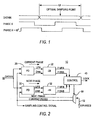
- FIG. 1 shows illustrative signal waveforms (all plotted along a common horizontal time scale) that are useful in explaining the invention.
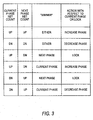
- FIG. 2 is a simplified schematic block diagram showing illustrative circuitry constructed in accordance with the invention.
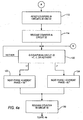
- FIG. 3 is a table showing illustrative modes of operation of circuitry of the type shown in FIG. 2 in accordance with the invention.
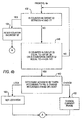
- FIGS. 4a-4b are collectively a simplified flow chart showing further illustrative aspects of operation of circuitry of the type shown in FIG. 2 in accordance with the invention.
- FIG. 5 shows more illustrative signal waveforms (all plotted along a common horizontal time scale) that are useful in explaining further aspects of the invention.
- FIG. 1 illustrates typical and representative signal conditions that can occur in either the prior systems mentioned in the background section of this specification or in a system in accordance with this invention.
- a serial data signal DATAIN represents successive bits of data. Each bit of data occupies one "unit interval" or "UI" in the data signal.
- the data signal does not necessarily transition (change in level) at the beginning and end of each UI, but all transitions in the data signal level are at the boundaries between UIs.
- both possible levels of DATAIN are shown for each UI, and the boundaries between UIs are indicated by the crosses to show where transitions can occur. Only one complete UI is shown in FIG. 1 , but it will be understood that this UI is preceded and followed by many other UIs in what is typically a long series of UIs, each of which is immediately adjacent to the preceding and following UIs in the series.
- FIG. 1 indicates the "optimal sampling point" for the representative UI shown in that FIG.
- the optimal sampling location is indicated to be the center of each UI. It will be understood, however, that in other systems the optimal sampling point may be somewhat earlier or somewhat later than the center of each UI. Any desired optimal sampling point can be accommodated by the present invention.
- FIG. 1 also shows two representative candidate clock signals on the same horizontal time axis as DATAIN.
- These two candidate clock signals are labelled "Phase X" and “Phase X + 45°", respectively.
- the Phase X and Phase X + 45° signals are two phase-adjacent ones of eight candidate clock signals. All of these signals have the same frequency, which in this example is equal to the bit rate of the DATAIN signal.
- Each of the eight candidate clock signals has a phase that is different from the phases of all of the other ones of those signals. These eight different phases are preferably equally distributed over one cycle of any one of the candidate clock signals. Thus the phase difference between any two phase-adjacent candidate clock signals is 45° in this example.
- eight signals with 45° phase spacing are employed in the illustrative embodiment shown and described herein, it will be understood that any number of such signals having any suitable phase spacing can be used instead if desired.
- phase detector circuitry is used to compare the phase of transitions in the DATAIN signal with the phase of transitions in candidate clock signals like those described above, taking the candidate signals one at a time. The objective is to find the one candidate clock signal having the phase that makes it best for use in timing the sampling of DATAIN to extract the data information from that signal.
- the prior phase detector circuitry may compare the phase of falling edges in a candidate clock signal with the phase of UI boundaries in the DATAIN signal.
- the candidate clock signal having falling edges that are closest in phase to UI boundaries has rising edges that are closest to the center of the UIs.
- FIG. 1 phase detector circuitry is used to compare the phase of transitions in the DATAIN signal with the phase of transitions in candidate clock signals like those described above, taking the candidate signals one at a time. The objective is to find the one candidate clock signal having the phase that makes it best for use in timing the sampling of DATAIN to extract the data information from that signal.
- the prior phase detector circuitry may compare the phase of falling edges in a candidate clock signal
- Phase X + 45° signal has falling edges that are closest in phase to UI boundaries in DATAIN.
- the rising edges in Phase X + 45° are therefore closest to the center of the UIs and thus have the best timing for use in controlling sampling of DATAIN.
- Phase X + 45° for use in controlling sampling of DATAIN, the above-described prior phase detector circuitry will, however, continue to detect that the falling edges in Phase X + 45° are actually somewhat later in time or phase than the UI boundaries in DATAIN. Eventually this will cause phase alignment circuitry of the above-described prior type to switch to the phase-adjacent candidate clock signal whose falling edges are earlier in time or phase than the UI boundaries in DATAIN. This means switching from Phase X + 45° to Phase X as the signal selected for controlling the timing of DATAIN signal sampling. Although probably still an acceptable choice, Phase X is not as good a choice as Phase X + 45° because the positive-going transitions in Phase X are farther from the center of UI than the positive-going transitions in Phase X + 45°.
- Phase X + 45° the signal for controlling sampling of DATAIN.
- phase alignment circuitry will continue to switch back and forth between Phase X + 45° and Phase X indefinitely (assuming that the UI boundaries in DATAIN remain between falling edges in these two candidate clock signals).
- This switching back and forth serves no useful purpose, and it may have such disadvantages as increasing noise in the system and increasing the risk of false interpretation of bits in DATAIN.
- FIG. 2 Illustrative dynamic phase alignment ("DPA") circuitry 10 in accordance with the present invention is shown in FIG. 2 .
- This circuitry includes two phase detector circuits 20 and 30. Each of phase detector circuits 20 and 30 receives the DATAIN signal via one of its inputs.
- the other input to phase detector 20 is the candidate clock signal currently being used to control sampling of DATAIN. This candidate clock signal is sometimes referred to herein as the "current phase” signal.
- the other input to phase detector 30 is the candidate clock signal (sometimes referred to as the "next phase” signal) that is adjacent in phase to the current phase signal and that the current phase circuitry (elements 20 and 22) are pointing to as a possibly (although not necessarily) better choice for use in controlling sampling of DATAIN. (The manner in which this "pointing" is done will be explained later in this specification.) For example, in the situation illustrated by FIG. 1 , the current phase signal might be Phase X + 45°, in which case the next phase signal would be Phase X.
- phase detector 20 detects that a transition in DATAIN is later in time than a negative-going transition in the current phase signal, circuitry 20 outputs an "up" signal pulse on its UPA output lead to indicate that a better phase match might be achieved by selecting as the current phase signal the candidate clock signal having greater phase angle than the candidate clock signal currently selected as the current phase signal. Conversely, if phase detector 20 detects that a transition in DATAIN is earlier in time than a negative-going transition in the current phase signal, circuitry 20 outputs a "down" signal pulse on its DNA output lead to indicate that a better phase match might be achieved by selecting as the current phase signal the candidate clock signal having a lower phase angle than the candidate clock signal currently selected as the current phase signal.
- Circuitry 22 may be counter and divider circuitry. Circuitry 22 counts up in response to each UPA pulse produced by circuitry 20. Circuitry 22 counts down in response to each DNA pulse. The count contained by circuitry 22 at any given time during counting operation of that circuitry is thus the net of the UPA and DNA pulses it has received since it was last reset. Circuitry 22 produces an output signal on an F UPA output lead whenever the net count contained in circuitry 22 is 28 UPA pulses. Circuitry 22 produces an output signal on an F DNA output lead whenever the net count contained in circuitry 22 is 28 DNA pulses. The counter in circuitry 22 may be reset to a neutral starting count each time such an F UPA or F DNA output signal is produced. A counter in circuitry 32 (described in more detail below) is also reset whenever the counter in circuitry 22 is reset.
- Circuitry 30 produces an UPB or DNB output pulse whenever a transition in DATAIN is later or earlier, respectively, than a negative-going transition in the next phase signal.
- Circuitry 32 forms a net count of the UPB and DNB pulses and outputs an F UPB or F DNB signal whenever the net count contained in circuitry 32 is 14 UPB or DNB pulses, respectively.
- the counter in circuitry 32 may be reset to a neutral starting count each time such an F UPB or F DNB output signal is produced.
- the counter in circuitry 32 may also be reset at other times, such as whenever the counter in circuitry 22 is reset.
- the integration operations performed by elements 22 and 32 prevent the system from trying to be too responsive to phase differences between DATAIN and the candidate clock signals applied to elements 20 and 30.
- the use of different thresholds in elements 22 and 32 (especially the use of a smaller threshold (e.g., 14) in element 32 than in element 22 (e.g., 28)) helps make the system more likely to lock on one phase than to switch arbitrarily between two phases as will be shown below. This further improves the stability of the system in accordance with the invention. (Later in this specification it will be explained that the difference in the thresholds mentioned above may not actually be as great as the difference between 28 and 14.)
- Control circuitry 40 receives all of the F UPA, F DNA, F UPB, and F DNB signals. On the basis of those signals, circuitry 40 controls multiplexer circuitry 50 to select the current phase signal and the next phase signal from among the eight candidate clock signals supplied to multiplexer circuitry 50 via leads 52.
- An illustrative selection control algorithm that control circuitry 40 may implement in accordance with the invention is shown in FIGS. 3 and 4a-4b .
- FIG. 3 Each horizontal line in FIG. 3 illustrates different possible conditions of the counts in circuits 22 and 32 when one or the other of those circuits reaches its threshold for outputting one of the F UPA, F DNA, F UPB, or F DNB signals.
- the channel with the circuit 22 or 32 thus outputting one of these signals is identified in the FIG. 3 column headed "Winner.”
- the two left-hand columns indicate the "polarity" of the concurrent net counts in circuits 22 and 32, respectively.
- the right-hand column indicates the current-phase action (if any) taken or commanded by circuitry 40 in response to the conditions indicated in the first three columns.
- FIGS. 4a-4b The possible, subsequent, next-phase action taken or commanded by circuitry 40 is illustrated by FIGS. 4a-4b , described later in this specification.
- control circuit 40 causes multiplexer 50 to select a higher phase candidate clock signal for the current phase signal. For example, if the current phase signal was Phase X and the next phase signal was Phase X + 45°, the new current phase signal would be Phase X + 45°. It will be apparent from this and the following discussion that to perform its function, control circuit 40 needs to receive not only signals telling it when one of circuits 22 and 32 has reached its threshold and from which direction, but also what the current state of the count in the other one of circuits 22 and 32 is.
- the F UPA, F DNA, F UPB, and F DNB signals can include signals indicating whether the count in the associated circuit 22 and 32 is currently trending up or trending down.
- the second line in FIG. 3 illustrates what may be thought of as a condition opposite that illustrated by the first line. This is a condition in which both of circuits 22 and 32 are registering net DN counts when either of those circuits reaches its threshold for outputting an F DNA or F DNB signal.
- control circuitry 40 causes multiplexer 50 to select for the current phase signal a candidate clock signal having lower phase. For example, if the current phase signal was Phase X and the next phase signal was Phase X + 45°, the current phase signal would become Phase X - 45°. As another example, if the current and next phase signals were Phase X + 45° and Phase X, respectively, the new current phase signal would be Phase X.
- the third line in FIG. 3 illustrates the following condition: Circuit 32 outputs an F DNB signal before circuit 22 reaches the count required for output of an F UPA signal. However, the net count in circuit 22 is UP. This indicates that the phase of DATAIN is between the phases of the current and next phase signals. It may additionally suggest that the phase of DATAIN is quite close to the phases of the current phase signal and farther from the phase of the next phase signal (because circuit 32 is receiving sufficiently predominant DNB pulses to reach its threshold count of 14, while circuit 22 is not receiving sufficiently predominant UPA pulses to (in the same time) reach its threshold count of 28). This further suggests that the current phase signal is already the best available choice for use in sampling DATAIN.
- control circuit 40 does not change the signal selections being made by multiplexer 50, and may in addition produce an output "LOCK” signal indicating to the circuitry making use of DPA circuitry 10 that the DPA circuitry is in a desirable, stable, "lock” condition.
- the fourth line in FIG. 3 illustrates a condition somewhat like the third line condition, except that in this case circuitry 22 reaches its UP threshold (28) and outputs an F UPA signal before circuitry 32 reaches its DN threshold (14).
- the phase of DATAIN is closer to the phase of the next phase signal than to the phase of the current phase signal.
- control circuit 40 causes multiplexer 50 to select the next higher phase candidate clock signal for the current phase signal. For example, if current phase was Phase X and next phase was Phase X + 45°, current phase becomes Phase X + 45°.
- the fifth line in FIG. 3 is somewhat like the third line, except that in this case the current phase signal has greater phase angle (e.g., Phase X + 45°) than the next phase signal (e.g. Phase X).
- Circuitry 32 reaches its UP threshold (14) and outputs an F UPB signal before circuitry 22 reaches its DN threshold (28).
- This condition indicates that the phase of DATAIN is between the current and next phases.
- this condition tends to suggest that the phase of DATAIN is closer to the current phase than to the next phase.
- Control circuitry 40 therefore makes no change in either the current phase signal or the next phase signal, and it may also output a "LOCK" signal as described above in connection with the third line in FIG. 3 .
- control circuitry 40 causes multiplexer 50 to select a new current phase signal having phase angle that is decreased relative to the previously selected current phase signal.
- the new next phase signal is subsequently determined by the polarity of an initial subsequent count of the counter in circuitry 22. This can be done in the manner illustrated by FIGS. 4a-4b .
- the counter in circuitry 32 is held in reset and only the counter in circuitry 22 is released (step 114).
- Steps 120, 122, 124, and 130 show that the counter in circuitry 32 is held in reset until the counter in circuitry 22 reaches +7 or -7. If +7 is reached, next phase is selected (by element 50 in FIG.
- next phase is selected (by element 50 in FIG. 2 ) as the current phase -45° (step 124).
- the counter in circuit 32 is released from reset (step 130). Using a threshold like +/-7 in the selection of next phase helps prevent next phase from switching around too much.
- the counters in circuits 22 and 32 compete by counting to 28 and 14, respectively (step 140).
- the step 132 intervening between steps 130 and 140 monitors the possibility of the counter in circuitry 22 falling below +7 or above -7. If that happens, the counter in circuitry 32 is reset (step 134) and the next phase selection process is repeated by returning to step 120.
- the threshold difference between circuits 22 and 32 is not as great as it may at first appear to be, because the counter in circuitry 22 is always given a head start of 7 before the counter in circuitry 32 is released to begin counting.
- the threshold difference between circuits 22 and 32 is therefore only 7, not 14 as it may superficially appear to be.
- step 140 determines the action to be taken according to FIG. 3 . If the action to be taken is a change in the current phase, that is done in step 152 and control then passes back to step 112. On the other hand, if the action to be taken is "lock,” that is done in step 150, after which control passes back to step 112.
- next phase threshold e.g., 14
- the current phase threshold e.g., effectively 21, after the head start of 7 given the counter in circuitry 22 before the counter in circuitry 32 is released to begin counting as described above
- Next phase should be farther from the phase of DATAIN than current phase.
- circuitry 32 should reach its relatively low threshold before circuitry 22 reaches its relatively high threshold, and under those conditions the system will "lock" (i.e., not change the selections of current phase and next phase).
- circuitry 22 reaches its high threshold (effectively 21) before circuitry 32 reaches its low threshold (14), there is a need to change the current and next phase signal selections because the current phase signal is not the best one for use in controlling when the DATAIN signal is sampled. It will be appreciated, however, that it may not be necessary for circuits 22 and 32 to have precisely this difference in thresholds. Good operation may be achieved with thresholds that are farther apart, not as far apart, or even equal to one another.
- FIGS. 3 and 4a-4b are only illustrative of how circuitry 40 may be arranged to respond to various conditions in the circuitry upstream from circuitry 40.
- circuitry of the invention Another desirable attribute of the circuitry of the invention is that its resolution tends to increase with jitter on the data.
- the circuit has the tendency to settle in the better of the two best phases with jitter on the data because jitter slows down the counter 22/32 that is closer to the optimal sampling point. This is illustrated by FIG. 5 .
- next phase is closer to the optimal sampling point.
- the next phase detector 30 will mostly be outputting DN pulses because next phase is somewhat above the optimal sampling point. However, because of the noise on the data, the next phase detector will also output some UP pulses. The closer next phase is to the sampling point, the more UP pulses will occur when compared to DN pulses. However, total DN pulses should be greater than UP pulses, assuming the jitter is distributed in a Gaussian distribution around the optimal sampling point and next phase is above the optimal sampling point. The UP pulses slow down the next phase counter 32 and make it more likely that the current phase path 20/22 will reach its threshold first, causing a switch to next phase.
- the current phase counter will be slowed down by the jitter, making the circuit more likely to lock.
- the end effect is that the circuit tends to settle in the phase whose falling edge is closer to the data transition point where the jitter is centered.
- candidate clock signals 52 are only illustrative, and a larger or smaller number of such signals can be used instead if desired.
- the candidate clock signals do not have to have the same frequency as the bit rate of the DATAIN signal.
- the candidate clock signals could have a frequency that is a multiple of (e.g., two, three, or four times) the bit rate.
- the current phase signal might not be used directly to control sampling of the DATAIN signal, but might instead be used as a pointer to another clock signal that is best for sampling the DATAIN signal.
- this other clock signal could be another of the candidate clock signals having a predetermined phase shift from the current phase signal.
Landscapes
- Synchronisation In Digital Transmission Systems (AREA)
- Dc Digital Transmission (AREA)
Claims (22)
- Schaltung für eine dynamische Phasenangleichung, die umfasst:eine Quelle (52) von mehr als zwei phasenverteilten Taktsignalen;eine Auswahlschaltung (50), um zwei phasenbenachbarte Taktsignale aus den Taktsignalen steuerbar auszuwählen;eine erste Phasendetektionsschaltung (20) zum Vergleichen der Zeitvorgabe des Auftretens von: [1] Übergängen in einem seriellen Datensignal; und [2] Übergängen in einem ersten der zwei phasenbenachbarten Taktsignale, und zum Erzeugen erster Ausgangsanzeigesignale (UPA, DNA), die angeben, ob diese Taktübergänge später oder früher sind als die Datenübergänge;eine zweite Phasendetektionsschaltung (30) zum Vergleichen der Zeitvorgabe des Auftretens von: [1] den Datenübergängen; und [2] Übergängen in einem zweiten der zwei phasenbenachbarten Taktsignale, und zum Erzeugen zweiter Ausgangsanzeigesignale (UPB, DNB), die angeben, ob diese Taktübergänge später oder früher sind als die Datenübergänge; undeine erste Integratorschaltung (22) zum Aufnehmen der ersten Ausgangsanzeigesignale und zum Erzeugen eines ersten Auslösesignals (F UPA, F DNA), wenn ihr Nettozählstand einen ersten Schwellenwert erreicht;eine zweite Integratorschaltung (32) zum Aufnehmen der zweiten Ausgangsanzeigesignale und zum Erzeugen eines zweiten Auslösesignals (F UPB, F DNB), wenn ihr Nettozählstand einen zweiten Schwellenwert erreicht; undeine Steuerschaltung (40), die in Reaktion auf das erste und das zweite Auslösesignal die Auswahlschaltung für Folgendes steuert:Behalten der ausgewählten zwei phasenbenachbarten Taktsignale mindestens auf der Basis davon, dass die Auswahlschaltung das zweite Auslösesignal früher als das erste Auslösesignal empfängt und entweder [1] der erste Nettozählstand anzeigt, dass die Taktübergänge in dem ersten Taktsignal des ausgewählten Paars Taktsignale netto früher sind als die Datenübergänge, und der zweite Nettozählstand anzeigt, dass die Taktübergänge in dem zweiten Taktsignal des ausgewählten Paars Taktsignale netto später sind als die Datenübergänge, oder [2] der erste Nettozählstand anzeigt, dass die Taktübergänge in dem ersten Taktsignal des ausgewählten Paars Taktsignale netto später sind als die Datenübergänge und der zweite Nettozählstand anzeigt, dass die Taktübergänge in dem zweiten Taktsignal des ausgewählten Paars Taktsignale netto früher sind als die Datenübergänge; undandernfalls Auswählen anderer phasenbenachbarter Paare der Taktsignale.
- Schaltung nach Anspruch 1, die ferner umfasst:eine Ausgabeschaltung zum Ausgeben des ersten der zwei phasenbenachbarten Taktsignale zur Verwendung als eine Basis zum Auswählen von Abtastzeiten des seriellen Datensignals, um Daten daraus wiederherzustellen.
- Schaltung nach Anspruch 1, wobei die Steuerschaltung keine Änderung an der Taktsignalauswahl vornimmt, die von der Auswahlschaltung vorgenommen wird, sofern nicht einer der Nettozählstande seinen jeweiligen Schwellenwert erreicht.
- Schaltung nach Anspruch 1, wobei die Steuerschaltung ein Sperrsignal ausgibt, um die Auswahlschaltung zu steuern, um die ausgewählten zwei phasenbenachbarten Taktsignale zu behalten.
- Verfahren für eine dynamische Phasenangleichung, das umfasst:Auswählen zweier phasenbenachbarter Taktsignale aus mehreren phasenverteilten Taktsignalen;Vergleichen der Zeitvorgabe des Auftretens von: [1] Übergängen in einem seriellen Datensignal; und [2] Übergängen in einem ersten der zwei phasenbenachbarten Taktsignale, und Erzeugen erster Ausgangsanzeigesignale (UPA, DNA), die angeben, ob diese Taktübergänge später oder früher sind als die Datenübergänge;Vergleichen der Zeitvorgabe des Auftretens von: [1] den Datenübergängen; und [2] Übergängen in einem zweiten der zwei phasenbenachbarten Taktsignale, und Erzeugen zweiter Ausgangsanzeigesignale (UPB, DNB), die angeben, ob diese Taktübergänge später oder früher sind als die Datenübergänge; undIntegrieren der ersten Ausgangsanzeigesignale, um einen ersten Nettozählstand zu erzeugen, und Ausgeben eines ersten Auslösesignals, wenn der erste Nettozählstand einen ersten Schwellenwert erreicht;Integrieren der zweiten Ausgangsanzeigesignale, um einen zweiten Nettozählstand zu erzeugen, und Ausgeben eines zweiten Auslösesignals, wenn der zweite Nettozählstand einen zweiten Schwellenwert erreicht; undBehalten der ausgewählten zwei phasenbenachbarten Taktsignale mindestens auf der Basis davon, dass die Auswahlschaltung das zweite Auslösesignal früher als das erste Auslösesignal empfängt und entweder [1] der erste Nettozählstand anzeigt, dass die Taktübergänge in dem ersten Taktsignal des ausgewählten Paars Taktsignale netto früher sind als die Datenübergänge, und der zweite Nettozählstand anzeigt, dass die Taktübergänge in dem zweiten Taktsignal des ausgewählten Paars Taktsignale netto später sind als die Datenübergänge oder [2] der erste Nettozählstand anzeigt, dass die Taktübergänge in dem ersten Taktsignal des ausgewählten Paars Taktsignale netto später sind als die Datenübergänge, und der zweite Nettozählstand anzeigt, dass die Taktübergänge in dem zweiten Taktsignal des ausgewählten Paars Taktsignale netto früher sind als die Datenübergänge; undandernfalls Auswählen anderer phasenbenachbarter Paare der Taktsignale.
- Verfahren nach Anspruch 5, das ferner umfasst:Auswählen des ersten der ausgewählten phasenbenachbarten Taktsignale als eine Basis zum Steuern einer Abtastzeitvorgabe des seriellen Datensignals, um Daten daraus wiederherzustellen.
- Verfahren nach Anspruch 5, das das Vergleichen ferner umfasst:Erzeugen eines ersten oder eines zweiten Ausgangsanzeigesignals jedes Mal, wenn sich die Phase des ersten ausgewählten Taktsignals jeweils auf einer ersten oder einer zweiten Seite der Phase des seriellen Datensignals befindet; undErzeugen eines dritten oder eines vierten Ausgangsanzeigesignals jedes Mal, wenn sich die Phase des zweiten ausgewählten Taktsignals jeweils auf einer ersten oder einer zweiten Seite der Phase des seriellen Datensignals befindet.
- Verfahren nach Anspruch 7, wobei der erste Nettozählstand von dem ersten und dem zweiten Ausgangsanzeigesignal gespeist wird; und wobei der zweite Nettozählstand von dem dritten und dem vierten Ausgangsanzeigesignal gespeist wird.
- Verfahren nach Anspruch 8, wobei das Vergleichen ferner umfasst:Erzeugen eines ersten Auslösesignals eines ersten Typs oder eines zweiten Typs immer dann, wenn der erste Nettozählstand gleich dem ersten Schwellenwert ist, da mehr erste Ausgangsanzeigesignale als zweite Ausgangsanzeigesignale auftreten bzw. umgekehrt; undErzeugen eines zweiten Auslösesignals eines ersten Typs oder eines zweiten Typs immer dann, wenn der zweite Nettozählstand gleich dem zweiten Schwellenwert ist, da mehr dritte Ausgangsanzeigesignale als vierte Ausgangsanzeigesignale auftreten bzw. umgekehrt.
- Verfahren nach Anspruch 9, wobei der erste und der zweite Schwellenwert verschieden sind.
- Verfahren nach Anspruch 10, das ferner umfasst:Auswählen des ersten ausgewählten Taktsignals als eine Basis zum Steuern einer Abtastzeitvorgabe des seriellen Datensignals, um Daten daraus wiederherzustellen.
- Verfahren nach Anspruch 11, wobei der erste Schwellenwert größer ist als der zweite Schwellenwert.
- Verfahren nach Anspruch 12, wobei das Ändern umfasst:Antworten auf ein beliebiges des ersten und des zweiten Auslösesignals, indem der Nettozählstand geprüft wird, der das erste oder das zweite Auslösesignal nicht verursacht hat.
- Verfahren nach Anspruch 13, wobei das Ändern ferner umfasst:Vornehmen einer Bestimmung davon, ob und wie mindestens eines der ausgewählten benachbarten Taktsignale geändert werden soll, basierend darauf, ob das erste oder das zweite Auslösesignal auf mehr ersten als zweiten Ausgangsanzeigesignalen oder auf mehr dritten als vierten Ausgangsanzeigesignalen bzw. umgekehrt beruht und ob der Nettozählstand, der das erste oder das zweite Auslösesignal nicht verursacht hat, mehr erste oder dritte Ausgangsanzeigesignale als zweite oder vierte Ausgangsanzeigesignale oder umgekehrt anzeigt.
- Verfahren nach Anspruch 14, wobei das Vornehmen der Bestimmung umfasst:Bestimmen, dass die ausgewählten benachbarten Taktsignale nicht geändert werden sollen, unter den folgenden Bedingungen: (1) ein zweites Auslösesignal des ersten Typs und der Nettozählstand, der das zweite Auslösesignal des ersten Typs nicht verursacht hat, zeigt mehr zweite Ausgangsanzeigesignale als erste Ausgangsanzeigesignale an, oder (2) ein zweites Auslösesignal des zweiten Typs und der Nettozählstand, der das zweite Auslösesignal des zweiten Typs nicht verursacht hat, zeigt mehr erste Ausgangsanzeigesignale als zweite Ausgangsanzeigesignale an.
- Verfahren nach Anspruch 15, das ferner umfasst:Erzeugen einer Sperranzeige unter den in Anspruch 15 spezifizierten Bedingungen.
- Schaltung nach Anspruch 1, wobei der erste Schwellenwert größer ist als der zweite Schwellenwert.
- Schaltung nach Anspruch 17, wobei die Steuerschaltung die Auswahlschaltung zumindest teilweise als Antwort auf die Nettozählstände der ersten und der zweiten Integratorschaltung steuert.
- Schaltung nach Anspruch 18, wobei die Steuerschaltung die ausgewählten benachbarten Taktsignale nur als Antwort auf einen Empfang eines der Auslösesignale ändern kann.
- Schaltung nach Anspruch 19, wobei die Steuerschaltung auf einen Empfang eines der Auslösesignale von entweder der ersten oder der zweiten Integratorschaltung damit antwortet, dass sie den Nettozählstand der anderen der ersten und der zweiten Integratorschaltung prüft.
- Schaltung nach Anspruch 20, wobei die Steuerschaltung bestimmt, ob und wie mindestens eines der ausgewählten benachbarten Taktsignale geändert werden soll, basierend darauf, welche der Integratorschaltungen das Auslösesignal lieferte und ob die andere Integratorschaltung mehr Später-Anzeigen als Früher-Anzeigen oder umgekehrt anzeigt.
- Schaltung nach Anspruch 21, wobei die Steuerschaltung die ausgewählten benachbarten Taktsignale unter den folgenden Bedingungen nicht als Antwort auf einen Empfang des zweiten Auslösesignals von der zweiten Integratorschaltung ändert: (1) das zweite Auslösesignal von der zweiten Integratorschaltung zeigt mehr Später-Anzeigen als Früher-Anzeigen an und der Nettozählstand der ersten Integratorschaltung zeigt mehr Früher-Anzeigen als Später-Anzeigen an, oder (2) das zweite Auslösesignal von der zweiten Integratorschaltung zeigt mehr Früher-Anzeigen als Später-Anzeigen an und die Nettozählstand der ersten Integratorschaltung zeigt mehr Später-Anzeigen als Früher-Anzeigen an.
Applications Claiming Priority (2)
| Application Number | Priority Date | Filing Date | Title |
|---|---|---|---|
| US10/849,319 US7453968B2 (en) | 2004-05-18 | 2004-05-18 | Dynamic phase alignment methods and apparatus |
| US849319 | 2004-05-18 |
Publications (2)
| Publication Number | Publication Date |
|---|---|
| EP1598939A1 EP1598939A1 (de) | 2005-11-23 |
| EP1598939B1 true EP1598939B1 (de) | 2014-07-16 |
Family
ID=34941318
Family Applications (1)
| Application Number | Title | Priority Date | Filing Date |
|---|---|---|---|
| EP05252993.0A Expired - Lifetime EP1598939B1 (de) | 2004-05-18 | 2005-05-16 | Verfahren und Vorrichtung zum dynamischen Phasenabgleich |
Country Status (4)
| Country | Link |
|---|---|
| US (2) | US7453968B2 (de) |
| EP (1) | EP1598939B1 (de) |
| JP (1) | JP2005333649A (de) |
| CN (2) | CN102594339B (de) |
Families Citing this family (14)
| Publication number | Priority date | Publication date | Assignee | Title |
|---|---|---|---|---|
| US7821312B1 (en) | 2007-04-18 | 2010-10-26 | Altera Corporation | Techniques for selecting phases of clock signals |
| TWI463865B (zh) * | 2007-11-23 | 2014-12-01 | Mstar Semiconductor Inc | 多切割之水平同步訊號之產生裝置及方法 |
| US8121219B1 (en) * | 2008-02-06 | 2012-02-21 | Link—A—Media Devices Corporation | Decision directed timing recovery using multiphase detection |
| JP5365132B2 (ja) * | 2008-10-17 | 2013-12-11 | 富士ゼロックス株式会社 | 直列信号の受信装置、直列伝送システム、直列伝送方法、直列信号の送信装置 |
| JP5229081B2 (ja) * | 2009-04-10 | 2013-07-03 | 富士通株式会社 | 半導体装置 |
| US8222920B2 (en) * | 2009-12-18 | 2012-07-17 | Meta Systems | Dynamic phase alignment |
| US8253451B1 (en) * | 2010-06-16 | 2012-08-28 | Xilinx, Inc. | Clock data recovery using phase accumulation over a time period defined by a number of cycles of a clock signal |
| US8707244B1 (en) | 2010-08-20 | 2014-04-22 | Altera Corporation | Methods and systems for performing signal activity extraction |
| US8368449B1 (en) | 2011-07-09 | 2013-02-05 | Altera Corporation | Dead zone detection for phase adjustment |
| JP5998612B2 (ja) | 2012-04-23 | 2016-09-28 | 富士通株式会社 | 補間回路および受信回路 |
| US8860475B1 (en) | 2013-03-29 | 2014-10-14 | Altera Corporation | Techniques for adjusting phases of clock signals |
| US9871504B2 (en) | 2016-02-16 | 2018-01-16 | Analog Devices, Inc. | Differential phase adjustment of clock input signals |
| US10218360B2 (en) * | 2016-08-02 | 2019-02-26 | Altera Corporation | Dynamic clock-data phase alignment in a source synchronous interface circuit |
| TWI727843B (zh) * | 2020-06-30 | 2021-05-11 | 瑞昱半導體股份有限公司 | 電子裝置之接收端及時脈回復操作之相位閥值的設定方法 |
Family Cites Families (26)
| Publication number | Priority date | Publication date | Assignee | Title |
|---|---|---|---|---|
| US4821297A (en) | 1987-11-19 | 1989-04-11 | American Telephone And Telegraph Company, At&T Bell Laboratories | Digital phase locked loop clock recovery scheme |
| CA2001266C (en) * | 1989-10-23 | 1996-08-06 | John Robert Long | Digital phase aligner and method for its operation |
| KR970002949B1 (ko) * | 1994-05-25 | 1997-03-13 | 삼성전자 주식회사 | 디지탈 통신시스템의 클럭발생방법 및 그 회로 |
| EP0758171A3 (de) * | 1995-08-09 | 1997-11-26 | Symbios Logic Inc. | Datenabtastung und -rückgewinnung |
| SE504920C2 (sv) * | 1995-09-29 | 1997-05-26 | Ericsson Telefon Ab L M | Förfarande och system för redundant klockdistribution till telekommunikationsutrustningar i vilka byte av vald klocksignal bland de inkommande klocksignalerna ständigt sker |
| US6266799B1 (en) * | 1997-10-02 | 2001-07-24 | Xaqti, Corporation | Multi-phase data/clock recovery circuitry and methods for implementing same |
| US6104222A (en) * | 1997-12-17 | 2000-08-15 | Sony Corporation | Flexible phase locked loop system |
| US6104228A (en) * | 1997-12-23 | 2000-08-15 | Lucent Technologies Inc. | Phase aligner system and method |
| US7227918B2 (en) * | 2000-03-14 | 2007-06-05 | Altera Corporation | Clock data recovery circuitry associated with programmable logic device circuitry |
| US20020090045A1 (en) * | 2001-01-10 | 2002-07-11 | Norm Hendrickson | Digital clock recovery system |
| US7366267B1 (en) | 2001-03-07 | 2008-04-29 | Altera Corporation | Clock data recovery with double edge clocking based phase detector and serializer/deserializer |
| US6650140B2 (en) * | 2001-03-19 | 2003-11-18 | Altera Corporation | Programmable logic device with high speed serial interface circuitry |
| US6553089B2 (en) * | 2001-03-20 | 2003-04-22 | Gct Semiconductor, Inc. | Fractional-N frequency synthesizer with fractional compensation method |
| US6704383B2 (en) * | 2001-03-20 | 2004-03-09 | Gct Semiconductor, Inc. | Sample and hold type fractional-N frequency synthesizer |
| US6750675B2 (en) * | 2001-09-17 | 2004-06-15 | Altera Corporation | Programmable logic devices with multi-standard byte synchronization and channel alignment for communication |
| US6941484B2 (en) * | 2002-03-01 | 2005-09-06 | Intel Corporation | Synthesis of a synchronization clock |
| DE10229130B3 (de) * | 2002-06-28 | 2004-02-05 | Advanced Micro Devices, Inc., Sunnyvale | PLL mit Automatischer Frequenzeinstellung |
| US7180972B1 (en) | 2002-10-16 | 2007-02-20 | Altera Corporation | Clock signal circuitry for multi-protocol high-speed serial interface circuitry |
| US6854044B1 (en) | 2002-12-10 | 2005-02-08 | Altera Corporation | Byte alignment circuitry |
| US7138837B2 (en) * | 2003-01-21 | 2006-11-21 | Altera Corporation | Digital phase locked loop circuitry and methods |
| US6724328B1 (en) * | 2003-06-03 | 2004-04-20 | Altera Corporation | Byte alignment for serial data receiver |
| US7272677B1 (en) | 2003-08-08 | 2007-09-18 | Altera Corporation | Multi-channel synchronization for programmable logic device serial interface |
| US7352835B1 (en) | 2003-09-22 | 2008-04-01 | Altera Corporation | Clock data recovery circuitry with dynamic support for changing data rates and a dynamically adjustable PPM detector |
| US7149914B1 (en) | 2003-09-26 | 2006-12-12 | Altera Corporation | Clock data recovery circuitry and phase locked loop circuitry with dynamically adjustable bandwidths |
| US7340021B1 (en) | 2003-11-13 | 2008-03-04 | Altera Corporation | Dynamic phase alignment and clock recovery circuitry |
| US7295641B1 (en) | 2003-11-26 | 2007-11-13 | Altera Corporation | Phase alignment circuitry and methods |
-
2004
- 2004-05-18 US US10/849,319 patent/US7453968B2/en not_active Expired - Fee Related
-
2005
- 2005-05-16 EP EP05252993.0A patent/EP1598939B1/de not_active Expired - Lifetime
- 2005-05-17 JP JP2005144787A patent/JP2005333649A/ja active Pending
- 2005-05-18 CN CN201210023025.4A patent/CN102594339B/zh not_active Expired - Fee Related
- 2005-05-18 CN CN2005100727337A patent/CN1700602B/zh not_active Expired - Fee Related
-
2008
- 2008-10-10 US US12/287,562 patent/US7623609B2/en not_active Expired - Fee Related
Also Published As
| Publication number | Publication date |
|---|---|
| US20090041170A1 (en) | 2009-02-12 |
| CN1700602A (zh) | 2005-11-23 |
| EP1598939A1 (de) | 2005-11-23 |
| US20050259775A1 (en) | 2005-11-24 |
| US7623609B2 (en) | 2009-11-24 |
| CN1700602B (zh) | 2012-03-14 |
| CN102594339A (zh) | 2012-07-18 |
| CN102594339B (zh) | 2015-07-08 |
| JP2005333649A (ja) | 2005-12-02 |
| US7453968B2 (en) | 2008-11-18 |
Similar Documents
| Publication | Publication Date | Title |
|---|---|---|
| US7623609B2 (en) | Dynamic phase alignment methods and apparatus | |
| US5278874A (en) | Phase lock loop frequency correction circuit | |
| US7349509B2 (en) | Multi rate clock data recovery based on multi sampling technique | |
| KR100944669B1 (ko) | 시험 장치 및 시험 방법 | |
| JP2003258782A (ja) | クロックリカバリ回路およびクロックリカバリ方法 | |
| US20070041485A1 (en) | Clock-signal adjusting method and device | |
| US20190379525A1 (en) | Automatic detection of change in pll locking trend | |
| US20100296615A1 (en) | Dynamic phase tracking using edge detection | |
| US5297869A (en) | Apparatus and method for synchronizing a digital data clock in a receiver with a digital data clock in a transmitter | |
| US8611487B2 (en) | Enhanced phase discriminator for fast phase alignment | |
| US9568890B1 (en) | All-digital delay-locked loop circuit based on time-to-digital converter and control method thereof | |
| US20020140472A1 (en) | Semiconductor device | |
| US5532632A (en) | Method and circuit for synchronizing an input data stream with a sample clock | |
| US6704882B2 (en) | Data bit-to-clock alignment circuit with first bit capture capability | |
| US7317775B1 (en) | Switched deskew on arbitrary data | |
| US6611219B1 (en) | Oversampling data recovery apparatus and method | |
| JP4808769B2 (ja) | 多ピンの非同期シリアル・インターフェースで転送されるデータを同期化するための方法及び装置 | |
| US20050135518A1 (en) | Improvements to data recovery circuits using oversampling for isi compensation | |
| WO2002084937A1 (en) | Synchronization detection apparatus | |
| US7773667B2 (en) | Pseudo asynchronous serializer deserializer (SERDES) testing | |
| US6704382B1 (en) | Self-sweeping autolock PLL | |
| US20100327925A1 (en) | Calibrating multiplying-delay-locked-loops (mdlls) | |
| US7375591B2 (en) | Robust false locking prevention in referenceless frequency acquisition | |
| US4955040A (en) | Method and apparatus for generating a correction signal in a digital clock recovery device | |
| KR20070065374A (ko) | 지연 제어 회로 및 방법 |
Legal Events
| Date | Code | Title | Description |
|---|---|---|---|
| PUAI | Public reference made under article 153(3) epc to a published international application that has entered the european phase |
Free format text: ORIGINAL CODE: 0009012 |
|
| AK | Designated contracting states |
Kind code of ref document: A1 Designated state(s): AT BE BG CH CY CZ DE DK EE ES FI FR GB GR HU IE IS IT LI LT LU MC NL PL PT RO SE SI SK TR |
|
| AX | Request for extension of the european patent |
Extension state: AL BA HR LV MK YU |
|
| 17P | Request for examination filed |
Effective date: 20060424 |
|
| AKX | Designation fees paid |
Designated state(s): AT BE BG CH CY CZ DE DK EE ES FI FR GB GR HU IE IS IT LI LT LU MC NL PL PT RO SE SI SK TR |
|
| GRAP | Despatch of communication of intention to grant a patent |
Free format text: ORIGINAL CODE: EPIDOSNIGR1 |
|
| INTG | Intention to grant announced |
Effective date: 20140206 |
|
| RAP1 | Party data changed (applicant data changed or rights of an application transferred) |
Owner name: ALTERA CORPORATION |
|
| GRAS | Grant fee paid |
Free format text: ORIGINAL CODE: EPIDOSNIGR3 |
|
| GRAA | (expected) grant |
Free format text: ORIGINAL CODE: 0009210 |
|
| AK | Designated contracting states |
Kind code of ref document: B1 Designated state(s): AT BE BG CH CY CZ DE DK EE ES FI FR GB GR HU IE IS IT LI LT LU MC NL PL PT RO SE SI SK TR |
|
| REG | Reference to a national code |
Ref country code: GB Ref legal event code: FG4D |
|
| REG | Reference to a national code |
Ref country code: CH Ref legal event code: EP |
|
| REG | Reference to a national code |
Ref country code: IE Ref legal event code: FG4D |
|
| REG | Reference to a national code |
Ref country code: AT Ref legal event code: REF Ref document number: 678171 Country of ref document: AT Kind code of ref document: T Effective date: 20140815 |
|
| REG | Reference to a national code |
Ref country code: DE Ref legal event code: R096 Ref document number: 602005044186 Country of ref document: DE Effective date: 20140828 |
|
| REG | Reference to a national code |
Ref country code: NL Ref legal event code: T3 |
|
| REG | Reference to a national code |
Ref country code: AT Ref legal event code: MK05 Ref document number: 678171 Country of ref document: AT Kind code of ref document: T Effective date: 20140716 |
|
| REG | Reference to a national code |
Ref country code: LT Ref legal event code: MG4D |
|
| PG25 | Lapsed in a contracting state [announced via postgrant information from national office to epo] |
Ref country code: BG Free format text: LAPSE BECAUSE OF FAILURE TO SUBMIT A TRANSLATION OF THE DESCRIPTION OR TO PAY THE FEE WITHIN THE PRESCRIBED TIME-LIMIT Effective date: 20141016 Ref country code: SE Free format text: LAPSE BECAUSE OF FAILURE TO SUBMIT A TRANSLATION OF THE DESCRIPTION OR TO PAY THE FEE WITHIN THE PRESCRIBED TIME-LIMIT Effective date: 20140716 Ref country code: ES Free format text: LAPSE BECAUSE OF FAILURE TO SUBMIT A TRANSLATION OF THE DESCRIPTION OR TO PAY THE FEE WITHIN THE PRESCRIBED TIME-LIMIT Effective date: 20140716 Ref country code: LT Free format text: LAPSE BECAUSE OF FAILURE TO SUBMIT A TRANSLATION OF THE DESCRIPTION OR TO PAY THE FEE WITHIN THE PRESCRIBED TIME-LIMIT Effective date: 20140716 Ref country code: GR Free format text: LAPSE BECAUSE OF FAILURE TO SUBMIT A TRANSLATION OF THE DESCRIPTION OR TO PAY THE FEE WITHIN THE PRESCRIBED TIME-LIMIT Effective date: 20141017 Ref country code: FI Free format text: LAPSE BECAUSE OF FAILURE TO SUBMIT A TRANSLATION OF THE DESCRIPTION OR TO PAY THE FEE WITHIN THE PRESCRIBED TIME-LIMIT Effective date: 20140716 Ref country code: PT Free format text: LAPSE BECAUSE OF FAILURE TO SUBMIT A TRANSLATION OF THE DESCRIPTION OR TO PAY THE FEE WITHIN THE PRESCRIBED TIME-LIMIT Effective date: 20141117 |
|
| PG25 | Lapsed in a contracting state [announced via postgrant information from national office to epo] |
Ref country code: IS Free format text: LAPSE BECAUSE OF FAILURE TO SUBMIT A TRANSLATION OF THE DESCRIPTION OR TO PAY THE FEE WITHIN THE PRESCRIBED TIME-LIMIT Effective date: 20141116 Ref country code: CY Free format text: LAPSE BECAUSE OF FAILURE TO SUBMIT A TRANSLATION OF THE DESCRIPTION OR TO PAY THE FEE WITHIN THE PRESCRIBED TIME-LIMIT Effective date: 20140716 Ref country code: PL Free format text: LAPSE BECAUSE OF FAILURE TO SUBMIT A TRANSLATION OF THE DESCRIPTION OR TO PAY THE FEE WITHIN THE PRESCRIBED TIME-LIMIT Effective date: 20140716 Ref country code: AT Free format text: LAPSE BECAUSE OF FAILURE TO SUBMIT A TRANSLATION OF THE DESCRIPTION OR TO PAY THE FEE WITHIN THE PRESCRIBED TIME-LIMIT Effective date: 20140716 |
|
| REG | Reference to a national code |
Ref country code: DE Ref legal event code: R097 Ref document number: 602005044186 Country of ref document: DE |
|
| PG25 | Lapsed in a contracting state [announced via postgrant information from national office to epo] |
Ref country code: CZ Free format text: LAPSE BECAUSE OF FAILURE TO SUBMIT A TRANSLATION OF THE DESCRIPTION OR TO PAY THE FEE WITHIN THE PRESCRIBED TIME-LIMIT Effective date: 20140716 Ref country code: DK Free format text: LAPSE BECAUSE OF FAILURE TO SUBMIT A TRANSLATION OF THE DESCRIPTION OR TO PAY THE FEE WITHIN THE PRESCRIBED TIME-LIMIT Effective date: 20140716 Ref country code: SK Free format text: LAPSE BECAUSE OF FAILURE TO SUBMIT A TRANSLATION OF THE DESCRIPTION OR TO PAY THE FEE WITHIN THE PRESCRIBED TIME-LIMIT Effective date: 20140716 Ref country code: EE Free format text: LAPSE BECAUSE OF FAILURE TO SUBMIT A TRANSLATION OF THE DESCRIPTION OR TO PAY THE FEE WITHIN THE PRESCRIBED TIME-LIMIT Effective date: 20140716 Ref country code: RO Free format text: LAPSE BECAUSE OF FAILURE TO SUBMIT A TRANSLATION OF THE DESCRIPTION OR TO PAY THE FEE WITHIN THE PRESCRIBED TIME-LIMIT Effective date: 20140716 Ref country code: IT Free format text: LAPSE BECAUSE OF FAILURE TO SUBMIT A TRANSLATION OF THE DESCRIPTION OR TO PAY THE FEE WITHIN THE PRESCRIBED TIME-LIMIT Effective date: 20140716 |
|
| PLBE | No opposition filed within time limit |
Free format text: ORIGINAL CODE: 0009261 |
|
| STAA | Information on the status of an ep patent application or granted ep patent |
Free format text: STATUS: NO OPPOSITION FILED WITHIN TIME LIMIT |
|
| 26N | No opposition filed |
Effective date: 20150417 |
|
| PG25 | Lapsed in a contracting state [announced via postgrant information from national office to epo] |
Ref country code: SI Free format text: LAPSE BECAUSE OF FAILURE TO SUBMIT A TRANSLATION OF THE DESCRIPTION OR TO PAY THE FEE WITHIN THE PRESCRIBED TIME-LIMIT Effective date: 20140716 |
|
| REG | Reference to a national code |
Ref country code: CH Ref legal event code: PL |
|
| GBPC | Gb: european patent ceased through non-payment of renewal fee |
Effective date: 20150516 |
|
| PG25 | Lapsed in a contracting state [announced via postgrant information from national office to epo] |
Ref country code: MC Free format text: LAPSE BECAUSE OF FAILURE TO SUBMIT A TRANSLATION OF THE DESCRIPTION OR TO PAY THE FEE WITHIN THE PRESCRIBED TIME-LIMIT Effective date: 20140716 Ref country code: LU Free format text: LAPSE BECAUSE OF FAILURE TO SUBMIT A TRANSLATION OF THE DESCRIPTION OR TO PAY THE FEE WITHIN THE PRESCRIBED TIME-LIMIT Effective date: 20150516 Ref country code: CH Free format text: LAPSE BECAUSE OF NON-PAYMENT OF DUE FEES Effective date: 20150531 Ref country code: LI Free format text: LAPSE BECAUSE OF NON-PAYMENT OF DUE FEES Effective date: 20150531 |
|
| REG | Reference to a national code |
Ref country code: IE Ref legal event code: MM4A |
|
| REG | Reference to a national code |
Ref country code: FR Ref legal event code: PLFP Year of fee payment: 12 |
|
| PG25 | Lapsed in a contracting state [announced via postgrant information from national office to epo] |
Ref country code: IE Free format text: LAPSE BECAUSE OF NON-PAYMENT OF DUE FEES Effective date: 20150516 Ref country code: GB Free format text: LAPSE BECAUSE OF NON-PAYMENT OF DUE FEES Effective date: 20150516 |
|
| PG25 | Lapsed in a contracting state [announced via postgrant information from national office to epo] |
Ref country code: BE Free format text: LAPSE BECAUSE OF FAILURE TO SUBMIT A TRANSLATION OF THE DESCRIPTION OR TO PAY THE FEE WITHIN THE PRESCRIBED TIME-LIMIT Effective date: 20140716 |
|
| REG | Reference to a national code |
Ref country code: FR Ref legal event code: PLFP Year of fee payment: 13 |
|
| PG25 | Lapsed in a contracting state [announced via postgrant information from national office to epo] |
Ref country code: HU Free format text: LAPSE BECAUSE OF FAILURE TO SUBMIT A TRANSLATION OF THE DESCRIPTION OR TO PAY THE FEE WITHIN THE PRESCRIBED TIME-LIMIT; INVALID AB INITIO Effective date: 20050516 |
|
| PG25 | Lapsed in a contracting state [announced via postgrant information from national office to epo] |
Ref country code: TR Free format text: LAPSE BECAUSE OF FAILURE TO SUBMIT A TRANSLATION OF THE DESCRIPTION OR TO PAY THE FEE WITHIN THE PRESCRIBED TIME-LIMIT Effective date: 20140716 |
|
| REG | Reference to a national code |
Ref country code: FR Ref legal event code: PLFP Year of fee payment: 14 |
|
| PGFP | Annual fee paid to national office [announced via postgrant information from national office to epo] |
Ref country code: DE Payment date: 20180502 Year of fee payment: 14 |
|
| PGFP | Annual fee paid to national office [announced via postgrant information from national office to epo] |
Ref country code: NL Payment date: 20180514 Year of fee payment: 14 Ref country code: FR Payment date: 20180501 Year of fee payment: 14 |
|
| REG | Reference to a national code |
Ref country code: DE Ref legal event code: R119 Ref document number: 602005044186 Country of ref document: DE |
|
| REG | Reference to a national code |
Ref country code: NL Ref legal event code: MM Effective date: 20190601 |
|
| PG25 | Lapsed in a contracting state [announced via postgrant information from national office to epo] |
Ref country code: NL Free format text: LAPSE BECAUSE OF NON-PAYMENT OF DUE FEES Effective date: 20190601 Ref country code: DE Free format text: LAPSE BECAUSE OF NON-PAYMENT OF DUE FEES Effective date: 20191203 |
|
| PG25 | Lapsed in a contracting state [announced via postgrant information from national office to epo] |
Ref country code: FR Free format text: LAPSE BECAUSE OF NON-PAYMENT OF DUE FEES Effective date: 20190531 |