EP1598448A1 - Lead-free bump and method for forming the same - Google Patents
Lead-free bump and method for forming the same Download PDFInfo
- Publication number
- EP1598448A1 EP1598448A1 EP03782895A EP03782895A EP1598448A1 EP 1598448 A1 EP1598448 A1 EP 1598448A1 EP 03782895 A EP03782895 A EP 03782895A EP 03782895 A EP03782895 A EP 03782895A EP 1598448 A1 EP1598448 A1 EP 1598448A1
- Authority
- EP
- European Patent Office
- Prior art keywords
- plating
- lead
- plated
- alloy film
- forming
- Prior art date
- Legal status (The legal status is an assumption and is not a legal conclusion. Google has not performed a legal analysis and makes no representation as to the accuracy of the status listed.)
- Withdrawn
Links
Images



Classifications
-
- H—ELECTRICITY
- H10—SEMICONDUCTOR DEVICES; ELECTRIC SOLID-STATE DEVICES NOT OTHERWISE PROVIDED FOR
- H10W—GENERIC PACKAGES, INTERCONNECTIONS, CONNECTORS OR OTHER CONSTRUCTIONAL DETAILS OF DEVICES COVERED BY CLASS H10
- H10W72/00—Interconnections or connectors in packages
- H10W72/20—Bump connectors, e.g. solder bumps or copper pillars; Dummy bumps; Thermal bumps
-
- C—CHEMISTRY; METALLURGY
- C25—ELECTROLYTIC OR ELECTROPHORETIC PROCESSES; APPARATUS THEREFOR
- C25D—PROCESSES FOR THE ELECTROLYTIC OR ELECTROPHORETIC PRODUCTION OF COATINGS; ELECTROFORMING; APPARATUS THEREFOR
- C25D21/00—Processes for servicing or operating cells for electrolytic coating
- C25D21/12—Process control or regulation
- C25D21/14—Controlled addition of electrolyte components
-
- C—CHEMISTRY; METALLURGY
- C25—ELECTROLYTIC OR ELECTROPHORETIC PROCESSES; APPARATUS THEREFOR
- C25D—PROCESSES FOR THE ELECTROLYTIC OR ELECTROPHORETIC PRODUCTION OF COATINGS; ELECTROFORMING; APPARATUS THEREFOR
- C25D3/00—Electroplating: Baths therefor
- C25D3/02—Electroplating: Baths therefor from solutions
- C25D3/56—Electroplating: Baths therefor from solutions of alloys
- C25D3/60—Electroplating: Baths therefor from solutions of alloys containing more than 50% by weight of tin
-
- C—CHEMISTRY; METALLURGY
- C25—ELECTROLYTIC OR ELECTROPHORETIC PROCESSES; APPARATUS THEREFOR
- C25D—PROCESSES FOR THE ELECTROLYTIC OR ELECTROPHORETIC PRODUCTION OF COATINGS; ELECTROFORMING; APPARATUS THEREFOR
- C25D5/00—Electroplating characterised by the process; Pretreatment or after-treatment of workpieces
- C25D5/48—After-treatment of electroplated surfaces
- C25D5/50—After-treatment of electroplated surfaces by heat-treatment
- C25D5/505—After-treatment of electroplated surfaces by heat-treatment of electroplated tin coatings, e.g. by melting
-
- H—ELECTRICITY
- H10—SEMICONDUCTOR DEVICES; ELECTRIC SOLID-STATE DEVICES NOT OTHERWISE PROVIDED FOR
- H10P—GENERIC PROCESSES OR APPARATUS FOR THE MANUFACTURE OR TREATMENT OF DEVICES COVERED BY CLASS H10
- H10P14/00—Formation of materials, e.g. in the shape of layers or pillars
- H10P14/40—Formation of materials, e.g. in the shape of layers or pillars of conductive or resistive materials
- H10P14/46—Formation of materials, e.g. in the shape of layers or pillars of conductive or resistive materials using a liquid
- H10P14/47—Electrolytic deposition, i.e. electroplating; Electroless plating
-
- H—ELECTRICITY
- H10—SEMICONDUCTOR DEVICES; ELECTRIC SOLID-STATE DEVICES NOT OTHERWISE PROVIDED FOR
- H10W—GENERIC PACKAGES, INTERCONNECTIONS, CONNECTORS OR OTHER CONSTRUCTIONAL DETAILS OF DEVICES COVERED BY CLASS H10
- H10W70/00—Package substrates; Interposers; Redistribution layers [RDL]
- H10W70/01—Manufacture or treatment
- H10W70/05—Manufacture or treatment of insulating or insulated package substrates, or of interposers, or of redistribution layers
- H10W70/093—Connecting or disconnecting other interconnections thereto or therefrom, e.g. connecting bond wires or bumps
-
- H—ELECTRICITY
- H10—SEMICONDUCTOR DEVICES; ELECTRIC SOLID-STATE DEVICES NOT OTHERWISE PROVIDED FOR
- H10W—GENERIC PACKAGES, INTERCONNECTIONS, CONNECTORS OR OTHER CONSTRUCTIONAL DETAILS OF DEVICES COVERED BY CLASS H10
- H10W72/00—Interconnections or connectors in packages
- H10W72/01—Manufacture or treatment
- H10W72/012—Manufacture or treatment of bump connectors, dummy bumps or thermal bumps
-
- H—ELECTRICITY
- H10—SEMICONDUCTOR DEVICES; ELECTRIC SOLID-STATE DEVICES NOT OTHERWISE PROVIDED FOR
- H10W—GENERIC PACKAGES, INTERCONNECTIONS, CONNECTORS OR OTHER CONSTRUCTIONAL DETAILS OF DEVICES COVERED BY CLASS H10
- H10W90/00—Package configurations
- H10W90/701—Package configurations characterised by the relative positions of pads or connectors relative to package parts
-
- H—ELECTRICITY
- H05—ELECTRIC TECHNIQUES NOT OTHERWISE PROVIDED FOR
- H05K—PRINTED CIRCUITS; CASINGS OR CONSTRUCTIONAL DETAILS OF ELECTRIC APPARATUS; MANUFACTURE OF ASSEMBLAGES OF ELECTRICAL COMPONENTS
- H05K3/00—Apparatus or processes for manufacturing printed circuits
- H05K3/30—Assembling printed circuits with electric components, e.g. with resistors
- H05K3/32—Assembling printed circuits with electric components, e.g. with resistors electrically connecting electric components or wires to printed circuits
- H05K3/34—Assembling printed circuits with electric components, e.g. with resistors electrically connecting electric components or wires to printed circuits by soldering
- H05K3/341—Surface mounted components
- H05K3/3431—Leadless components
- H05K3/3436—Leadless components having an array of bottom contacts, e.g. pad grid array or ball grid array components
-
- H—ELECTRICITY
- H05—ELECTRIC TECHNIQUES NOT OTHERWISE PROVIDED FOR
- H05K—PRINTED CIRCUITS; CASINGS OR CONSTRUCTIONAL DETAILS OF ELECTRIC APPARATUS; MANUFACTURE OF ASSEMBLAGES OF ELECTRICAL COMPONENTS
- H05K3/00—Apparatus or processes for manufacturing printed circuits
- H05K3/30—Assembling printed circuits with electric components, e.g. with resistors
- H05K3/32—Assembling printed circuits with electric components, e.g. with resistors electrically connecting electric components or wires to printed circuits
- H05K3/34—Assembling printed circuits with electric components, e.g. with resistors electrically connecting electric components or wires to printed circuits by soldering
- H05K3/346—Solder materials or compositions specially adapted therefor
-
- H—ELECTRICITY
- H10—SEMICONDUCTOR DEVICES; ELECTRIC SOLID-STATE DEVICES NOT OTHERWISE PROVIDED FOR
- H10W—GENERIC PACKAGES, INTERCONNECTIONS, CONNECTORS OR OTHER CONSTRUCTIONAL DETAILS OF DEVICES COVERED BY CLASS H10
- H10W72/00—Interconnections or connectors in packages
- H10W72/01—Manufacture or treatment
- H10W72/012—Manufacture or treatment of bump connectors, dummy bumps or thermal bumps
- H10W72/01231—Manufacture or treatment of bump connectors, dummy bumps or thermal bumps using blanket deposition
- H10W72/01233—Manufacture or treatment of bump connectors, dummy bumps or thermal bumps using blanket deposition in liquid form, e.g. spin coating, spray coating or immersion coating
- H10W72/01235—Manufacture or treatment of bump connectors, dummy bumps or thermal bumps using blanket deposition in liquid form, e.g. spin coating, spray coating or immersion coating by plating, e.g. electroless plating or electroplating
-
- H—ELECTRICITY
- H10—SEMICONDUCTOR DEVICES; ELECTRIC SOLID-STATE DEVICES NOT OTHERWISE PROVIDED FOR
- H10W—GENERIC PACKAGES, INTERCONNECTIONS, CONNECTORS OR OTHER CONSTRUCTIONAL DETAILS OF DEVICES COVERED BY CLASS H10
- H10W72/00—Interconnections or connectors in packages
- H10W72/20—Bump connectors, e.g. solder bumps or copper pillars; Dummy bumps; Thermal bumps
- H10W72/251—Materials
-
- H—ELECTRICITY
- H10—SEMICONDUCTOR DEVICES; ELECTRIC SOLID-STATE DEVICES NOT OTHERWISE PROVIDED FOR
- H10W—GENERIC PACKAGES, INTERCONNECTIONS, CONNECTORS OR OTHER CONSTRUCTIONAL DETAILS OF DEVICES COVERED BY CLASS H10
- H10W72/00—Interconnections or connectors in packages
- H10W72/90—Bond pads, in general
-
- H—ELECTRICITY
- H10—SEMICONDUCTOR DEVICES; ELECTRIC SOLID-STATE DEVICES NOT OTHERWISE PROVIDED FOR
- H10W—GENERIC PACKAGES, INTERCONNECTIONS, CONNECTORS OR OTHER CONSTRUCTIONAL DETAILS OF DEVICES COVERED BY CLASS H10
- H10W72/00—Interconnections or connectors in packages
- H10W72/90—Bond pads, in general
- H10W72/941—Dispositions of bond pads
- H10W72/9415—Dispositions of bond pads relative to the surface, e.g. recessed, protruding
-
- H—ELECTRICITY
- H10—SEMICONDUCTOR DEVICES; ELECTRIC SOLID-STATE DEVICES NOT OTHERWISE PROVIDED FOR
- H10W—GENERIC PACKAGES, INTERCONNECTIONS, CONNECTORS OR OTHER CONSTRUCTIONAL DETAILS OF DEVICES COVERED BY CLASS H10
- H10W72/00—Interconnections or connectors in packages
- H10W72/90—Bond pads, in general
- H10W72/951—Materials of bond pads
- H10W72/952—Materials of bond pads comprising metals or metalloids, e.g. PbSn, Ag or Cu
Definitions
- the present invention relates to a lead-free bump and a method of forming the same, and more particularly to a lead-free bump with suppressed formation of voids, obtained by reflow a plated film of Sn-Ag solder alloy having an adjusted Ag content, and a method of forming the lead-free bumps, and also to a plating apparatus for forming such lead-free bumps.
- soldering In surface mounting technology of semiconductor devices or the like, it is very important to carry out soldering with high reliability.
- a heating operation is usually carried out to make plated films into the form of balls.
- the reflow temperature is preferably as low as possible in order to avoid thermal damage to other parts that exist in the substrate. From this viewpoint, many developments of solder alloys have been directed to making the composition of an alloy closest possible to the eutectic composition of the alloy in order to make use of the eutectic point.
- bumps by electroplating has the problem that upon reflow of bumps, voids can be formed in the bumps.
- the formation of voids is particularly marked with bumps of an Sn-Ag alloy, lowering the reliability of the bumps.
- the present invention has been accomplished based on the above findings.
- the present invention provides a lead-free bump obtained by forming an Sn-Ag alloy film having an Ag content lower than that of an Sn-Ag eutectic composition by plating and reflow the plated alloy film.
- the present invention also provide a method of forming a lead-free bump comprising: carrying out Sn-Ag alloy plating on a portion on which a bump is formed while controlling the composition of a plating bath and electrodeposition conditions so that a plated Sn-Ag alloy film having an Ag content lower than that of the Sn-Ag eutectic composition is formed; and then reflowing the plated alloy film.
- the present invention also provides a plating apparatus for forming a lead-free bump, comprising: a plating vessel for containing a plating solution having Ag ions and Sn ions; an anode; a holder for holding a workpiece and feeding electricity to the workpiece; an electrodeposition power source for feeding electricity to the anode and to the workpiece held by the holder; a replenishment mechanism for replenishing the plating solution with Ag ions and Sn ions; an analyzer for monitoring Ag ions and Sn ions; and a control mechanism for controlling, on a basis of analytical information from the analyzer, an Ag content in a plated Sn-Ag alloy film formed on a surface of the workpiece at a value lower than an Ag content of an Sn-Ag eutectic composition.
- the lead-free bump of the present invention can be obtained by depositing a plated Sn-Ag alloy film by Sn-Ag alloy plating (hereinafter referred to simply as "alloy plating") carried out under such controlled electrodeposition conditions that the plated Sn-Ag alloy film has an Ag content which is lower than the Ag content of the Sn-Ag eutectic composition (i. e. 3.5 wt%), and then reflowing the plated Sn-Ag alloy film into solder balls.
- alloy plating Sn-Ag alloy plating
- the Ag content in the plated alloy film is preferably made not higher than 2.6% by mass.
- the reflow temperature be not so high (for example, the maximum reflow temperature of not higher than 240°C).
- the lower limit of the Ag content in the plated alloy film be made 1.6% by mass.
- the Ag content in the plated alloy film is preferably made within the range of 1.6 to 2.6% by mass.
- the present invention it is necessary to carry out plating while controlling the Ag content in the plated alloy film at a value lower than 3.5% by mass, preferably from 1.6 to 2.6% by mass.
- the level of ⁇ -rays emitted from the surface of the plated alloy film is preferably not higher than 0.02 cph/cm 2 .
- Lead has a plurality of isotopes, including natural radioactive elements.
- the isotopes of lead are intermediate products or final products in uranium or thorium decay series and emit ⁇ -rays in their decay processes.
- the ⁇ -rays can act on semiconductor devices of a semiconductor integrated circuit and cause soft errors.
- Sn and other elements also contain such natural radioactive elements though in a slight amount.
- a lead-free Sn-Ag bump also emits ⁇ -rays, and it is important to suppress the emission of ⁇ -rays at a low level. By suppressing the emission of ⁇ -rays from the surface of the lead-free bump at a level of not higher than 0.02 cph/cm 2 , soft errors in semiconductor integrated circuit devices due to the influence of ⁇ -rays can be prevented.
- the composition of deposited components in alloy plating is determined by the concentrations of the components in a plating solution and the electrodeposition conditions.
- the Ag content in a plated alloy film can be made within the above-described range by adjusting the concentration ratio of Ag ion to Sn ion in an alloy plating solution, and controlling the electrodeposition conditions.
- the Ag content in a plated alloy film can be controlled by (a) changing the electrodeposition conditions while keeping the concentration ratio of Ag ion to Sn ion in a plating bath constant, or (b) by changing the concentration ratio of Ag ion to Sn ion in a plating bath while keeping the electrodeposition conditions constant.
- the alloy plating solution generally contains, besides the ions of the metals forming an alloy, a complexing agent for stabilizing metal ions, a brightening agent for making the surface of the plated film beautiful and/or other additive (s), the Ag content in the plated alloy film is primarily determined by the concentration ratio of Ag ion to Sn ion in the alloy plating bath.
- a plated alloy film having a controlled Ag content can be obtained by finding a preferred range of the concentration ratio of Ag ion to Sn ion though experiments, and carrying out plating while keeping the concentration ratio within the preferred range.
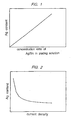
- the Ag content in a plated alloy film is proportional to the concentration ratio of Ag ion to Sn ion in a plating solution, as schematically shown in Fig. 1.
- a plated alloy film having a controlled Ag content can be obtained by immersing a workpiece in an alloy plating solution with a predetermined concentration ratio of Ag ion to Sn ion, and carrying out plating under constant electrodeposition conditions. By reflowing the plated alloy film, a bump without voids can be obtained.
- composition An alloy plating solution usable in the present invention.
- alloy plating it is known that, in alloy plating, the composition of deposited components varies depending on the electrodeposition conditions. Also in alloy plating according to the present invention, the Ag content in a plated alloy film can be changed by changing the electrodeposition conditions.
- Alloy plating according to the present invention may be carried out in various manners using various types of electric currents, including direct current plating carried out by continuously applying a direct current, and an intermittent plating carried out by intermittently applying a direct current with periodical rest periods.
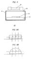
- the Ag content in the plated alloy film decreases with an increase in the current density, as schematically shown in FIG. 2.
- Preferable current conditions may be determined experimentally, and plating may be carried out while keeping the determined conditions.
- a preferred current density in direct current plating is about 10 to 100 mA/cm 2 .
- the plated alloy film has an Ag content which is different from the Ag content of a plated alloy film as obtained by applying the same direct current continuously.
- preferable conditions such as an applied voltage, the proportion of rest time, etc. may be determined experimentally, and plating may be carried out while keeping the determined conditions.
- a preferred current density during application of electric current is about 10-200 mA/cm 2
- a preferred rest time (zero current) is 1/10 - 1 of application time.
- each applied voltage in the above two types of plating varies depending upon conditions such as the intensity of current, the underlying material, the thickness of plating, the plating solution, the anode used, etc., it is preferably about 1 to 5 V.
- an apparatus for carrying out the above-described alloy plating there is no particular limitation on an apparatus for carrying out the above-described alloy plating, and a common dip type plating apparatus may be employed.
- a common dip type plating apparatus may be employed.
- an apparatus which takes account of a jig structure configured to the mechanical conditions of a workpiece, a stirring mechanism (paddle structure) for supplying metal ions uniformly and rapidly to the entire surface of a workpiece such as a wafer, the shape and size of a mask for equalizing the electric field distribution, a plating solution circulation system for removing foreign matter, preventing a change in the quality of a plating solution and supplying metal ions uniformly and rapidly to the entire surface of a workpiece, etc.
- a plating apparatus which is provided with a replenishment mechanism for replenishing an alloy plating solution with Ag ions and Sn ions, an analyzer for monitoring Ag ions and Sn ions, and a control mechanical which, based on analytical information from the analyzer, adjusts the concentrations of Ag ions and Sn ions in the alloy plating solution and/or controls the electrodeposition conditions.
- FIG. 4 shows an example of such a plating apparatus.
- reference numeral 1 denotes a plating apparatus
- 2 denotes a plating vessel
- 3 denotes an anode
- 4 denotes a holder
- 5 denotes a workpiece
- 6 denotes an electrodeposition power source
- 7 denotes conductive wire
- 8a through 8c denote a replenishment mechanism
- 9 denotes an analyzer
- 10 denotes a control mechanism
- 11 denotes an auto-sampler
- 12a through 12c denote feed pumps
- 13 denotes a shut-off valve
- 14 denotes a discharge outlet.
- the analyzer 9 periodically or continuously analyzes and monitors a change in the concentrations of Ag ions and Sn ions, as an index for control of plating, which is due to consumption or loss of the ions during operation of the plating apparatus.
- An atomic absorption spectrometry device for example, may be used as the analyzer 9.
- the control mechanism 10 which comprises, for example, a computer for control, determines optimum replenishment amounts of Ag ions (solution), Sn ions (solution), etc. based on analytical information from the analyzer 9, and actuates the feed bumps 12a through 12c, which are connected to the replenishment mechanisms 8a through 8c, so as to add Ag ions (solution) and Sn ions (solution) to a plating solution.
- the replenishment mechanisms 8a through 8c may additionally comprise a portion for replenishing water for adjustment of the composition of plating solution, or an additive.
- the anode 3, the holder 4 and the plating vessel 2 are each made of a material whose emission of ⁇ -rays is low so that the amount of ⁇ -rays emitted from the surface of a plated Sn-Ag alloy film formed by the plating apparatus 1 is made not higher than 0.02 cph/cm 2 .
- the amount of natural radioactive elements taken in a bump of the plated alloy film formed by plating is made low, so that the amount of ⁇ -rays emitted from the bump can be made at such a low level. This effectively suppresses soft errors in semiconductor integrated circuit devices due to the influence of ⁇ -rays.
- the anode 3 may either be an insoluble anode or a soluble anode. It is possible with an insoluble anode to continue using it without a change.
- Sn soluble anode is used as the anode 3
- Sn ions can be supplied from the anode to the plating solution during plating operation. This facilitates control of the plating solution and reduces operation for replenishment of metal ions.
- the control mechanism 10 desirably controls the plating system under optimum electrodeposition conditions (the above-described current density and voltage application method) for a particular composition of plating solution, and should make at least one of control of the electrodeposition conditions and control of the concentrations of Ag ions and Sn ions by replenishment of the ions.
- the actual deposition behavior of plating is influenced not only by the above-described concentration ratio of Ag ion to Sn ion in an alloy plating solution and the electrodeposition conditions, but also by many other factors.
- the Ag content in a plated alloy film can vary depending on the type of the additive (s) added in the plating solution. In most cases, however, the specific ingredients and their amounts of an additive are undisclosed as the additive manufacturer's know-how.
- the plated alloy film thus formed is then subjected to reflowing to form a bump.
- the reflowing is carried out by heating the plated alloy film in an inert gas atmosphere (e.g. nitrogen or argon atmosphere) using, for example, the apparatus (infrared oven) shown in FIG. 5.
- an inert gas atmosphere e.g. nitrogen or argon atmosphere
- FIG. 5 reference numeral 20 denotes an infrared oven, 21 denotes a chamber, 22 denotes a stage, 23 denotes a silica glass window, 24 denotes an infrared lamp, and 25 denotes a workpiece.
- the reflowing in this apparatus is carried out, for example, by setting the workpiece 25, which has undergone alloy plating, in the chamber 21, allowing nitrogen gas to flow into the chamber 21 at a rate of about 8 to 30 L/min to adequately carry out gas replacement, and then heating the workpiece 25 through the silica glass window 23 by the infrared lamp 24.
- the reflow temperature is important for the formation of bumps according to the present invention.
- a bump may be formed on a printed circuit board, etc.
- Common electronic components are said to be heat-resistant to a temperature of about 240°C.
- the maximum temperature in the step of reflowing a plated alloy film formed by alloy plating should therefore be not higher than 240°C.
- the melting point of an Sn-Ag solder is generally 221°C, and it is generally said that the minimum reflowable temperature is the melting point +10°C, and that the reflow temperature must be maintained for 15 to 45 seconds. Taking such requirements into consideration, the temperature conditions upon reflowing may be exemplified by: 231°C for 30 seconds with the maximum temperature of 238°C.
- the above-described lead-free bump of the present invention can be utilized, for example, as a ball-shaped bump on wiring pad in a mounting substrate.
- metal bond pads are first formed, and then a resist is applied on the substrate, with locations for bumps being left, to form a resist pattern.
- plated Sn-Ag alloy films having a controlled Ag content are formed in the above-describedmanner. Thereafter, the resist is peeled off, and the alloy films are subjected to reflowing at a predetermined reflow temperature.
- any one of the formation of the metal bond pads, the formation of the resist pattern and the removal of the resist may be carried out by common methods in the art.
- lead-free bump of the present invention can be used to form wiring pads on a variety of semiconductor substrates.
- lead-free bumps can be formed on a semiconductor substrate of a semiconductor device by the following steps (I) to (IV):
- the semiconductor device used in step (I) includes an integrated circuit (IC) and the like.
- a known barrier metal may be used as the barrier metal formed on the wiring pads in step (II).
- a resist was applied to a thickness of 120 ⁇ m on a wafer in such a manner that a number of holes having an opening size of 100 ⁇ m are formed, thereby preparing a sample.
- the plating area of the sample was 149.63 cm 2 .
- Plating of the sample was carried out by the following steps under the following conditions.
- Alloy plating was carried out with various proportions of Ag to the total metal in an alloy plating solution, various current densities upon plating and various current application methods, and the respective plated alloy films were subjected to reflowing at 238°C.
- measurement of the Ag content and observation of the shape of bump and the presence of voids were carried out in the same manner as in Example 1. The results are shown in table 1.
- voids are not formed in a bump (plated alloy film) when the Ag content is 2.9 % or lower. Especially when the Ag content is from 1.8 to 2.6 %, the plated alloy film can be transformed into a ball at the maximum reflow temperature 238°C without formation of voids, providing a highly practical lead-free bump.
- Lead-free bumps according to the present invention are free of voids, and are of a desirable ball shape that can be formed at a relatively low reflow temperature. Further, those bumps do not contain lead, and thus do not cause malfunction of an integrated circuit due to the emission of ⁇ -rays nor environmental contamination.
- Lead-free bumps according to the present invention can therefore be widely used in surface mounting technology (SMT) of semiconductor devices, etc. and enable a reliable soldering despite their no inclusion of lead.
- SMT surface mounting technology
- the present invention relates to a lead-free bump with suppressed formation of voids, obtained by reflowing a plated film of Sn-Ag solder alloy having an adjusted Ag content, and a method of forming the same.
Landscapes
- Chemical & Material Sciences (AREA)
- Engineering & Computer Science (AREA)
- Chemical Kinetics & Catalysis (AREA)
- Electrochemistry (AREA)
- Materials Engineering (AREA)
- Metallurgy (AREA)
- Organic Chemistry (AREA)
- Automation & Control Theory (AREA)
- Electroplating Methods And Accessories (AREA)
- Electroplating And Plating Baths Therefor (AREA)
- Electric Connection Of Electric Components To Printed Circuits (AREA)
Abstract
The present invention relates to a lead-free bump with suppressed formation of voids, obtained by reflowing a plated film of Sn-Ag solder alloy having an adjusted Ag content, and a method of forming the lead-free bump. The lead-free bump of the present invention is obtained by forming an Sn-Ag alloy film having an Ag content lower than that of an Sn-Ag eutectic composition by plating and reflowing the plated alloy film. <IMAGE>
Description
The present invention relates to a lead-free bump and a
method of forming the same, and more particularly to a lead-free
bump with suppressed formation of voids, obtained by reflow a
plated film of Sn-Ag solder alloy having an adjusted Ag content,
and a method of forming the lead-free bumps, and also to a plating
apparatus for forming such lead-free bumps.
In surface mounting technology of semiconductor devices
or the like, it is very important to carry out soldering with
high reliability. Although an eutectic solder containing lead
(Sn:Pb = 63:37) has heretofore been used widely in soldering,
in the light of environmental contamination and because of the
problem of α-rays generation from lead, development of lead-free
soldering is under way.
For example, lead-free soldering by means of printing or
electroplating is being studied. With printing, however, there
is a limit in its approach to fine pitches through the use of
a metal mask. Electroplating is therefore becoming mainstream,
for example, for the formation of wafer bumps.
In the case of forming wafer bumps by electroplating, a
heating operation (reflow) is usually carried out to make plated
films into the form of balls. The reflow temperature is
preferably as low as possible in order to avoid thermal damage
to other parts that exist in the substrate. From this viewpoint,
many developments of solder alloys have been directed to making
the composition of an alloy closest possible to the eutectic
composition of the alloy in order to make use of the eutectic
point.
However, the formation of bumps by electroplating has the
problem that upon reflow of bumps, voids can be formed in the
bumps. The formation of voids is particularly marked with bumps
of an Sn-Ag alloy, lowering the reliability of the bumps.
There is, therefore, a need for the development of a means
to form lead-free Sn-Ag bumps by electroplating without
formation of voids after reflow, and it is an object of the present
invention to provide such means.
As a result of studies to obtain lead-free bumps without
formation of voids, it was discovered by the present inventors
that when forming bumps by Sn-Ag solder alloy plating, the Ag
content in the plated film has a great influence on the formation
of voids. In particular, voids will be formed in a lead-free
Sn-Ag bump after reflow when the Ag content of the bump is
approximately equal to or higher than the Ag content of the Sn-Ag
eutectic composition. As a result of further study, it has now
been found that in order to securely prevent the formation of
voids in Sn-Ag solder bumps, it is necessary to form the plated
bumps having a lower Ag content than that of the Sn-Ag eutectic
composition (weight ratio Sn : Ag = 96.5 : 3.5 /Ag content, 3.5%
by mass).
It has also been found that contrary to the expectation
that a decrease in the Ag content of a plated alloy film from
the Ag content of the Sn-Ag eutectic composition will incur a
rise in the reflow temperature, the melting point of the alloy
film does not increase significantly with a decrease in the Ag
content, that is, it is not necessary to significantly raise the
reflow temperature.
The present invention has been accomplished based on the
above findings. Thus, the present invention provides a
lead-free bump obtained by forming an Sn-Ag alloy film having
an Ag content lower than that of an Sn-Ag eutectic composition
by plating and reflow the plated alloy film.
The present invention also provide a method of forming a
lead-free bump comprising: carrying out Sn-Ag alloy plating on
a portion on which a bump is formed while controlling the
composition of a plating bath and electrodeposition conditions
so that a plated Sn-Ag alloy film having an Ag content lower than
that of the Sn-Ag eutectic composition is formed; and then
reflowing the plated alloy film.
The present invention also provides a plating apparatus
for forming a lead-free bump, comprising: a plating vessel for
containing a plating solution having Ag ions and Sn ions; an
anode; a holder for holding a workpiece and feeding electricity
to the workpiece; an electrodeposition power source for feeding
electricity to the anode and to the workpiece held by the holder;
a replenishment mechanism for replenishing the plating solution
with Ag ions and Sn ions; an analyzer for monitoring Ag ions and
Sn ions; and a control mechanism for controlling, on a basis of
analytical information from the analyzer, an Ag content in a
plated Sn-Ag alloy film formed on a surface of the workpiece at
a value lower than an Ag content of an Sn-Ag eutectic composition.
The lead-free bump of the present invention can be obtained
by depositing a plated Sn-Ag alloy film by Sn-Ag alloy plating
(hereinafter referred to simply as "alloy plating") carried out
under such controlled electrodeposition conditions that the
plated Sn-Ag alloy film has an Ag content which is lower than
the Ag content of the Sn-Ag eutectic composition (i. e. 3.5 wt%),
and then reflowing the plated Sn-Ag alloy film into solder balls.
From the viewpoint of preventing the formation of voids,
it may be sufficient merely to control the Ag content in the plated
alloy film such that it is lower than the above-described upper
limit. With the Ag content ranging from 2.6 to 3.5% by mass,
however, voids could be formed in some cases. Thus, in order
to completely avoid voids, the Ag content in the plated alloy
film is preferably made not higher than 2.6% by mass.
Further, it is desirable from a practical viewpoint that
the reflow temperature be not so high (for example, the maximum
reflow temperature of not higher than 240°C). For this purpose,
it is preferred that the lower limit of the Ag content in the
plated alloy film be made 1.6% by mass. Thus, in order to provide
practically desirable bumps, the Ag content in the plated alloy
film is preferably made within the range of 1.6 to 2.6% by mass.
Thus, according to the present invention, it is necessary
to carry out plating while controlling the Ag content in the
plated alloy film at a value lower than 3.5% by mass, preferably
from 1.6 to 2.6% by mass.
Further, with respect to the lead-free bump obtained by
reflowing the plated alloy film as described above, the level
of α-rays emitted from the surface of the plated alloy film is
preferably not higher than 0.02 cph/cm2.
Lead has a plurality of isotopes, including natural
radioactive elements. The isotopes of lead are intermediate
products or final products in uranium or thorium decay series
and emit α-rays in their decay processes. The α-rays can act
on semiconductor devices of a semiconductor integrated circuit
and cause soft errors. Sn and other elements also contain such
natural radioactive elements though in a slight amount. Thus,
a lead-free Sn-Ag bump also emits α-rays, and it is important
to suppress the emission of α-rays at a low level. By suppressing
the emission of α-rays from the surface of the lead-free bump
at a level of not higher than 0.02 cph/cm2, soft errors in
semiconductor integrated circuit devices due to the influence
of α-rays can be prevented.
In general, the composition of deposited components in
alloy plating is determined by the concentrations of the
components in a plating solution and the electrodeposition
conditions. Also in alloy plating according to the present
invention, the Ag content in a plated alloy film can be made within
the above-described range by adjusting the concentration ratio
of Ag ion to Sn ion in an alloy plating solution, and controlling
the electrodeposition conditions. In particular, the Ag content
in a plated alloy film can be controlled by (a) changing the
electrodeposition conditions while keeping the concentration
ratio of Ag ion to Sn ion in a plating bath constant, or (b) by
changing the concentration ratio of Ag ion to Sn ion in a plating
bath while keeping the electrodeposition conditions constant.
Though the alloy plating solution generally contains,
besides the ions of the metals forming an alloy, a complexing
agent for stabilizing metal ions, a brightening agent for making
the surface of the plated film beautiful and/or other additive (s),
the Ag content in the plated alloy film is primarily determined
by the concentration ratio of Ag ion to Sn ion in the alloy plating
bath. Thus, a plated alloy film having a controlled Ag content
can be obtained by finding a preferred range of the concentration
ratio of Ag ion to Sn ion though experiments, and carrying out
plating while keeping the concentration ratio within the
preferred range. In fact, it has been confirmed that when
carrying out alloy plating under fixed electrodeposition
conditions, the Ag content in a plated alloy film is proportional
to the concentration ratio of Ag ion to Sn ion in a plating
solution, as schematically shown in Fig. 1.
Accordingly, a plated alloy film having a controlled Ag
content can be obtained by immersing a workpiece in an alloy
plating solution with a predetermined concentration ratio of Ag
ion to Sn ion, and carrying out plating under constant
electrodeposition conditions. By reflowing the plated alloy
film, a bump without voids can be obtained.
The following is an example of an alloy plating solution
usable in the present invention;
Composition:
Composition:
It is known that, in alloy plating, the composition of
deposited components varies depending on the electrodeposition
conditions. Also in alloy plating according to the present
invention, the Ag content in a plated alloy film can be changed
by changing the electrodeposition conditions.
Alloy plating according to the present invention may be
carried out in various manners using various types of electric
currents, including direct current plating carried out by
continuously applying a direct current, and an intermittent
plating carried out by intermittently applying a direct current
with periodical rest periods.
In the case of direct current plating in which a direct
current is applied continuously during plating, the Ag content
in the plated alloy film decreases with an increase in the current
density, as schematically shown in FIG. 2. Preferable current
conditions may be determined experimentally, and plating may be
carried out while keeping the determined conditions. A
preferred current density in direct current plating is about 10
to 100 mA/cm2.
In the case of intermittent plating in which a direct
current is applied intermittently with periodical rest periods,
as schematically shown in FIG. 3, the plated alloy film has an
Ag content which is different from the Ag content of a plated
alloy film as obtained by applying the same direct current
continuously. Also with intermittent plating, preferable
conditions, such as an applied voltage, the proportion of rest
time, etc. may be determined experimentally, and plating may be
carried out while keeping the determined conditions. A
preferred current density during application of electric current
is about 10-200 mA/cm2, and a preferred rest time (zero current)
is 1/10 - 1 of application time.
Though each applied voltage in the above two types of
plating varies depending upon conditions such as the intensity
of current, the underlying material, the thickness of plating,
the plating solution, the anode used, etc., it is preferably about
1 to 5 V.
There is no particular limitation on an apparatus for
carrying out the above-described alloy plating, and a common dip
type plating apparatus may be employed. For a practical
operation, however, it is desirable to use an apparatus which
takes account of a jig structure configured to the mechanical
conditions of a workpiece, a stirring mechanism (paddle
structure) for supplying metal ions uniformly and rapidly to the
entire surface of a workpiece such as a wafer, the shape and size
of a mask for equalizing the electric field distribution, a
plating solution circulation system for removing foreign matter,
preventing a change in the quality of a plating solution and
supplying metal ions uniformly and rapidly to the entire surface
of a workpiece, etc.
Further, as described above, it is necessary to carry out
alloy plating while adjusting the concentrations of Ag ions and
Sn ions in a plating solution, and controlling the
electrodeposition conditions. It is therefore preferred to use
a plating apparatus which is provided with a replenishment
mechanism for replenishing an alloy plating solution with Ag ions
and Sn ions, an analyzer for monitoring Ag ions and Sn ions, and
a control mechanical which, based on analytical information from
the analyzer, adjusts the concentrations of Ag ions and Sn ions
in the alloy plating solution and/or controls the
electrodeposition conditions. FIG. 4 shows an example of such
a plating apparatus.
In FIG. 4, reference numeral 1 denotes a plating apparatus,
2 denotes a plating vessel, 3 denotes an anode, 4 denotes a holder,
5 denotes a workpiece, 6 denotes an electrodeposition power
source, 7 denotes conductive wire, 8a through 8c denote a
replenishment mechanism, 9 denotes an analyzer, 10 denotes a
control mechanism, 11 denotes an auto-sampler, 12a through 12c
denote feed pumps, 13 denotes a shut-off valve, and 14 denotes
a discharge outlet.
The analyzer 9 periodically or continuously analyzes and
monitors a change in the concentrations of Ag ions and Sn ions,
as an index for control of plating, which is due to consumption
or loss of the ions during operation of the plating apparatus.
An atomic absorption spectrometry device, for example, may be
used as the analyzer 9.
The control mechanism 10, which comprises, for example,
a computer for control, determines optimum replenishment amounts
of Ag ions (solution), Sn ions (solution), etc. based on
analytical information from the analyzer 9, and actuates the feed
bumps 12a through 12c, which are connected to the replenishment
mechanisms 8a through 8c, so as to add Ag ions (solution) and
Sn ions (solution) to a plating solution.
The replenishment mechanisms 8a through 8c, besides the
portion for replenishment of Ag ion solution and Sn ion solution,
may additionally comprise a portion for replenishing water for
adjustment of the composition of plating solution, or an
additive.
The anode 3, the holder 4 and the plating vessel 2 are each
made of a material whose emission of α-rays is low so that the
amount of α-rays emitted from the surface of a plated Sn-Ag alloy
film formed by the plating apparatus 1 is made not higher than
0.02 cph/cm2. Thus, the amount of natural radioactive elements
taken in a bump of the plated alloy film formed by plating is
made low, so that the amount of α-rays emitted from the bump can
be made at such a low level. This effectively suppresses soft
errors in semiconductor integrated circuit devices due to the
influence of α-rays.
The anode 3 may either be an insoluble anode or a soluble
anode. It is possible with an insoluble anode to continue using
it without a change. When an Sn soluble anode is used as the
anode 3, Sn ions can be supplied from the anode to the plating
solution during plating operation. This facilitates control of
the plating solution and reduces operation for replenishment of
metal ions.
The control mechanism 10 desirably controls the plating
system under optimum electrodeposition conditions (the
above-described current density and voltage application method)
for a particular composition of plating solution, and should make
at least one of control of the electrodeposition conditions and
control of the concentrations of Ag ions and Sn ions by
replenishment of the ions.
The actual deposition behavior of plating is influenced
not only by the above-described concentration ratio of Ag ion
to Sn ion in an alloy plating solution and the electrodeposition
conditions, but also by many other factors. For example, the
Ag content in a plated alloy film can vary depending on the type
of the additive (s) added in the plating solution. In most cases,
however, the specific ingredients and their amounts of an
additive are undisclosed as the additive manufacturer's
know-how.
For forming bumps according to the present inventions,
therefore, it is necessary to conduct experiments in advance with
varying current densities in electroplating, voltage
application methods and the concentration ratios of Ag ions to
Sn ion in an alloy plating solution, and measure the contents
of Ag in the various bumps formed. Based on the results of
measurement, the optimum conditions for plating can be
determined.
By carrying out plating under the optimum conditions thus
determined, it becomes possible to stabilize the composition of
the plating solution and stably form a bump having a desired Ag
content.
The plated alloy film thus formed is then subjected to
reflowing to form a bump. The reflowing is carried out by heating
the plated alloy film in an inert gas atmosphere (e.g. nitrogen
or argon atmosphere) using, for example, the apparatus (infrared
oven) shown in FIG. 5. In FIG. 5, reference numeral 20 denotes
an infrared oven, 21 denotes a chamber, 22 denotes a stage, 23
denotes a silica glass window, 24 denotes an infrared lamp, and
25 denotes a workpiece.
The reflowing in this apparatus is carried out, for example,
by setting the workpiece 25, which has undergone alloy plating,
in the chamber 21, allowing nitrogen gas to flow into the chamber
21 at a rate of about 8 to 30 L/min to adequately carry out gas
replacement, and then heating the workpiece 25 through the silica
glass window 23 by the infrared lamp 24.
The reflow temperature is important for the formation of
bumps according to the present invention. A bump may be formed
on a printed circuit board, etc. Common electronic components
are said to be heat-resistant to a temperature of about 240°C.
The maximum temperature in the step of reflowing a plated alloy
film formed by alloy plating should therefore be not higher than
240°C. Further, the melting point of an Sn-Ag solder is
generally 221°C, and it is generally said that the minimum
reflowable temperature is the melting point +10°C, and that the
reflow temperature must be maintained for 15 to 45 seconds.
Taking such requirements into consideration, the temperature
conditions upon reflowing may be exemplified by: 231°C for 30
seconds with the maximum temperature of 238°C.
The above-described lead-free bump of the present
invention can be utilized, for example, as a ball-shaped bump
on wiring pad in a mounting substrate.
In the formation of ball-shaped bumps, metal bond pads are
first formed, and then a resist is applied on the substrate, with
locations for bumps being left, to form a resist pattern. Next,
plated Sn-Ag alloy films having a controlled Ag content are formed
in the above-describedmanner. Thereafter, the resist is peeled
off, and the alloy films are subjected to reflowing at a
predetermined reflow temperature.
Any one of the formation of the metal bond pads, the
formation of the resist pattern and the removal of the resist
may be carried out by common methods in the art.
Further, the lead-free bump of the present invention can
be used to form wiring pads on a variety of semiconductor
substrates. In particular, lead-free bumps can be formed on a
semiconductor substrate of a semiconductor device by the
following steps (I) to (IV):
The semiconductor device used in step (I) includes an
integrated circuit (IC) and the like. A known barrier metal may
be used as the barrier metal formed on the wiring pads in step
(II).
The following examples are provided to illustrate the
present invention in greater detail and are not to be construed
to be limiting the invention in any manner.
A resist was applied to a thickness of 120 µm on a wafer
in such a manner that a number of holes having an opening size
of 100 µm are formed, thereby preparing a sample. The plating
area of the sample was 149.63 cm2. Plating of the sample was
carried out by the following steps under the following
conditions.
Degassing (10 min) → Pre-cleaning with 10 % sulfuric acid
(1 min) → Copper plating → Water-cleaning → Ni plating →
Water-cleaning → Sn-Ag alloy plating
| cu2+ | 220 g/L |
| H2SO4 | 200 g/ |
| HCl | |
| 5 mL/ | |
| Additive | |
| 5 mL/L |
| Ni (NH2SPO4) · 4H2O | 450 g/L |
| H3BO3 | 30 g/L |
| NiCl2 · 6H2O | 10 g/ |
| Additive | |
| 2 mL/L |
| Sn2+ | 40 g/L |
| Ag+ | 1.5 g/L |
| methanesulfonic acid | 100 g/L |
| Additive | 10 g/L |
Alloy plating was carried out with various proportions of
Ag to the total metal in an alloy plating solution, various
current densities upon plating and various current application
methods, and the respective plated alloy films were subjected
to reflowing at 238°C. For the bump thus obtained, measurement
of the Ag content and observation of the shape of bump and the
presence of voids were carried out in the same manner as in Example
1. The results are shown in table 1.
| Plating solution Ag/Sn (%) | Plating conditions Current density (A/dm2) | Voltage application method | Bump Ag content (wt%) | Void present (x) absent (o) | Ball formation at 238°C |
| 9.3 | 3 | DC | 5.2 | x | o |
| 4.4 | 3 | DC | 6.4 | x | o |
| 4.4 | 20 | CHOP | 4.0 | x | o |
| 4.3 | 3 | DC | 7.7 | x | o |
| 4.3 | 20 | CHOP | 5.1 | x | o |
| 1.3 | 3 | DC | 1.8 | o | o |
| 1.3 | 8 | DC | 0.9 | o | x |
| 1.3 | 20 | CHOP | 1.4 | o | x |
| 2.2 | 3 | DC | 3.4 | x | o |
| 2.2 | 20 | CHOP | 2.1 | o | o |
| 4.1 | 3 | DC | 4.9 | x | o |
| 3.1 | 20 | CHOP | 2.9 | o | o |
| 3.1 | 10 | CHOP | 3.6 | x | o |
| 3.1 | 3 | DC | 5.0 | x | o |
| 3.2 | 3 | DC | 5.8 | x | o |
| 3.2 | 20 | CHOP | 2.7 | x | o |
| 2.3 | 3 | DC | 3.5 | x | o |
| 2.3 | 20 | CHOP | 2.6 | o | o |
| Note: DC denotes direct current plating, and CHOP denotes intermittent plating |
As apparent from the results shown in Table 1, voids are
not formed in a bump (plated alloy film) when the Ag content is
2.9 % or lower. Especially when the Ag content is from 1.8 to
2.6 %, the plated alloy film can be transformed into a ball at
the maximum reflow temperature 238°C without formation of voids,
providing a highly practical lead-free bump.
Lead-free bumps according to the present invention are free
of voids, and are of a desirable ball shape that can be formed
at a relatively low reflow temperature. Further, those bumps
do not contain lead, and thus do not cause malfunction of an
integrated circuit due to the emission of α-rays nor
environmental contamination.
Lead-free bumps according to the present invention can
therefore be widely used in surface mounting technology (SMT)
of semiconductor devices, etc. and enable a reliable soldering
despite their no inclusion of lead.
The present invention relates to a lead-free bump with
suppressed formation of voids, obtained by reflowing a plated
film of Sn-Ag solder alloy having an adjusted Ag content, and
a method of forming the same.
Claims (17)
- A lead-free bump obtained by forming an Sn-Ag alloy film having an Ag content lower than that of an Sn-Ag eutectic composition by plating and reflow the plated alloy film.
- The lead-free bump according to claim 1, wherein the Ag content in the plated Sn-Ag alloy film is 1.6 to 2.6% by mass.
- The lead-free bump according to claim 1, wherein the maximum temperature of the reflow of the plated alloy film is not higher than 240°C.
- The lead-free bump according to claim 1, wherein the Ag content in the plated alloy film is adjusted to be lower than the Ag content of the Sn-Ag eutectic composition by controlling a composition of a plating bath and electrodeposition conditions.
- The lead-free bump according to claim 1, wherein the amount of α-rays emitted from a surface of the bump is not higher than 0.02 cph/cm2.
- A method of forming a lead-free bump comprising:carrying out Sn-Ag alloy plating on a portion on which a bump is formed while controlling the composition of a plating bath and electrodeposition conditions so that a plated Sn-Ag alloy film having an Ag content lower than that of the Sn-Ag eutectic composition is formed; and thenreflowing the plated alloy film.
- The method of forming a lead-free bump according to claim 6, wherein the Ag content in the plated Sn-Ag alloy film is 1.6 to 2.6% by mass.
- The method of forming a lead-free bump according to claim 7, wherein the maximum temperature of the reflowing the plated alloy film is not higher than 240°C.
- The method of forming a lead-free bump according to claim 6, wherein the control of the composition of the plating bath and the electrodeposition conditions is carried out by changing the electrodeposition conditions while keeping the ratio of concentration of Ag ion to Sn ion in the plating bath constant.
- The method of forming a lead-free bump according to claim 6, wherein the control of the composition of the plating bath and the electrodeposition conditions is carried out by changing the concentration ratio of Ag ion to Sn ion in the plating bath while keeping the electrodeposition conditions constant.
- A plating apparatus for forming a lead-free bump, comprising:a plating vessel for containing a plating solution having Ag ions and Sn ions;an anode;a holder for holding a workpiece and feeding electricity to the workpiece;an electrodeposition power source for feeding electricity to the anode and to the workpiece held by the holder;a replenishment mechanism for replenishing the plating solution with Ag ions and Sn ions;an analyzer for monitoring Ag ions and Sn ions; anda control mechanism for controlling, on a basis of analytical information from the analyzer, an Ag content in a plated Sn-Ag alloy film formed on a surface of the workpiece at a value lower than an Ag content of an Sn-Ag eutectic composition.
- The plating apparatus for forming a lead-free bump according to claim 11, wherein the Ag content in the plated Sn-Ag alloy film is controlled within the range of 1. 6 to 2.6% by mass.
- The plating apparatus for forming a lead-free bump according to claim 11, wherein the Ag content in the plated Sn-Ag alloy film is controlled by adjustment of concentrations of Ag ions and Sn ions in the plating solution and/or change of electrodeposition conditions.
- The plating apparatus for forming a lead-free bump according to claim 11, wherein the anode, the holder and the plating vessel are made of materials whose radiant quantity of α-rays is low so that a quantity of α-rays emitted from a surface of the plated Sn-Ag alloy film is made not higher than 0.02 cph/cm2 .
- The plating apparatus for forming a lead-free bump according to claim 11, wherein the anode comprises an insoluble anode.
- The plating apparatus for forming a lead-free bump according to claim 11, wherein the anode comprises a soluble anode.
- The plating apparatus for forming a lead-free bump according to claim 16, wherein the anode comprises an Sn anode.
Applications Claiming Priority (3)
| Application Number | Priority Date | Filing Date | Title |
|---|---|---|---|
| JP2002378010 | 2002-12-26 | ||
| JP2002378010 | 2002-12-26 | ||
| PCT/JP2003/016720 WO2004059042A1 (en) | 2002-12-26 | 2003-12-25 | Lead-free bump and method for forming the same |
Publications (2)
| Publication Number | Publication Date |
|---|---|
| EP1598448A1 true EP1598448A1 (en) | 2005-11-23 |
| EP1598448A4 EP1598448A4 (en) | 2007-03-07 |
Family
ID=32677413
Family Applications (1)
| Application Number | Title | Priority Date | Filing Date |
|---|---|---|---|
| EP03782895A Withdrawn EP1598448A4 (en) | 2002-12-26 | 2003-12-25 | LEAD-FREE BOSS AND METHOD FOR FORMING THE SAME |
Country Status (7)
| Country | Link |
|---|---|
| US (2) | US7012333B2 (en) |
| EP (1) | EP1598448A4 (en) |
| JP (1) | JP4425799B2 (en) |
| KR (1) | KR101076819B1 (en) |
| CN (1) | CN1732291B (en) |
| TW (1) | TWI303463B (en) |
| WO (1) | WO2004059042A1 (en) |
Families Citing this family (44)
| Publication number | Priority date | Publication date | Assignee | Title |
|---|---|---|---|---|
| US7012333B2 (en) * | 2002-12-26 | 2006-03-14 | Ebara Corporation | Lead free bump and method of forming the same |
| EP2381015B1 (en) | 2005-08-12 | 2019-01-16 | Modumetal, Inc. | Compositionally modulated composite materials |
| US7713859B2 (en) * | 2005-08-15 | 2010-05-11 | Enthone Inc. | Tin-silver solder bumping in electronics manufacture |
| TW200804629A (en) * | 2006-07-05 | 2008-01-16 | Idx Corp | Power supply for anodizing |
| US8177945B2 (en) * | 2007-01-26 | 2012-05-15 | International Business Machines Corporation | Multi-anode system for uniform plating of alloys |
| CA2730229C (en) | 2008-07-07 | 2017-02-14 | John D. Whitaker | Property modulated materials and methods of making the same |
| US9524945B2 (en) | 2010-05-18 | 2016-12-20 | Taiwan Semiconductor Manufacturing Company, Ltd. | Cu pillar bump with L-shaped non-metal sidewall protection structure |
| JP5311656B2 (en) * | 2008-12-27 | 2013-10-09 | 京セラSlcテクノロジー株式会社 | Wiring board |
| EP3009532A1 (en) | 2009-06-08 | 2016-04-20 | Modumetal, Inc. | Electrodeposited nanolaminate coatings and claddings for corrosion protection |
| US8841766B2 (en) | 2009-07-30 | 2014-09-23 | Taiwan Semiconductor Manufacturing Company, Ltd. | Cu pillar bump with non-metal sidewall protection structure |
| US8377816B2 (en) * | 2009-07-30 | 2013-02-19 | Taiwan Semiconductor Manufacturing Company, Ltd. | Method of forming electrical connections |
| US8324738B2 (en) | 2009-09-01 | 2012-12-04 | Taiwan Semiconductor Manufacturing Company, Ltd. | Self-aligned protection layer for copper post structure |
| US8659155B2 (en) * | 2009-11-05 | 2014-02-25 | Taiwan Semiconductor Manufacturing Company, Ltd. | Mechanisms for forming copper pillar bumps |
| US8610270B2 (en) * | 2010-02-09 | 2013-12-17 | Taiwan Semiconductor Manufacturing Company, Ltd. | Semiconductor device and semiconductor assembly with lead-free solder |
| US8441124B2 (en) | 2010-04-29 | 2013-05-14 | Taiwan Semiconductor Manufacturing Company, Ltd. | Cu pillar bump with non-metal sidewall protection structure |
| US9018758B2 (en) | 2010-06-02 | 2015-04-28 | Taiwan Semiconductor Manufacturing Company, Ltd. | Cu pillar bump with non-metal sidewall spacer and metal top cap |
| EP2596150B1 (en) | 2010-07-22 | 2020-06-17 | Modumetal, Inc. | Material and process for electrochemical deposition of nanolaminated brass alloys |
| US8546254B2 (en) | 2010-08-19 | 2013-10-01 | Taiwan Semiconductor Manufacturing Company, Ltd. | Mechanisms for forming copper pillar bumps using patterned anodes |
| US20120325671A2 (en) * | 2010-12-17 | 2012-12-27 | Tel Nexx, Inc. | Electroplated lead-free bump deposition |
| US9017528B2 (en) | 2011-04-14 | 2015-04-28 | Tel Nexx, Inc. | Electro chemical deposition and replenishment apparatus |
| US9005409B2 (en) | 2011-04-14 | 2015-04-14 | Tel Nexx, Inc. | Electro chemical deposition and replenishment apparatus |
| JP5876767B2 (en) * | 2012-05-15 | 2016-03-02 | 株式会社荏原製作所 | Plating apparatus and plating solution management method |
| EP2971265A4 (en) | 2013-03-15 | 2016-12-14 | Modumetal Inc | NANOSAFTIFIED CHROMIUM AND NICKEL COATING HAVING HIGH HARDNESS |
| HK1220741A1 (en) | 2013-03-15 | 2017-05-12 | Modumetal, Inc. | Nanolaminate coatings |
| CA2905536C (en) | 2013-03-15 | 2023-03-07 | Modumetal, Inc. | Electrodeposited compositions and nanolaminated alloys for articles prepared by additive manufacturing processes |
| CA2905575C (en) | 2013-03-15 | 2022-07-12 | Modumetal, Inc. | A method and apparatus for continuously applying nanolaminate metal coatings |
| WO2016044720A1 (en) | 2014-09-18 | 2016-03-24 | Modumetal, Inc. | A method and apparatus for continuously applying nanolaminate metal coatings |
| US9303329B2 (en) | 2013-11-11 | 2016-04-05 | Tel Nexx, Inc. | Electrochemical deposition apparatus with remote catholyte fluid management |
| US8877630B1 (en) * | 2013-11-12 | 2014-11-04 | Chipmos Technologies Inc. | Semiconductor structure having a silver alloy bump body and manufacturing method thereof |
| US9368340B2 (en) | 2014-06-02 | 2016-06-14 | Lam Research Corporation | Metallization of the wafer edge for optimized electroplating performance on resistive substrates |
| BR112017005534A2 (en) | 2014-09-18 | 2017-12-05 | Modumetal Inc | Methods of preparing articles by electrodeposition processes and additive manufacturing |
| CN105256347B (en) * | 2015-11-17 | 2018-01-16 | 通富微电子股份有限公司 | Tin-silver convex block argentiferous amount control method |
| JP6713809B2 (en) * | 2016-03-31 | 2020-06-24 | 株式会社荏原製作所 | Substrate manufacturing method and substrate |
| EP3510185A1 (en) | 2016-09-08 | 2019-07-17 | Modumetal, Inc. | Processes for providing laminated coatings on workpieces, and articles made therefrom |
| EP3509812B1 (en) | 2016-09-09 | 2025-04-09 | Modumetal, Inc. | Manufacturing of molds by deposition of material layers on a workpiece, molds and articles obtained by said process |
| CN109963966B (en) | 2016-09-14 | 2022-10-11 | 莫杜美拓有限公司 | System for reliable, high-throughput, complex electric field generation and method of producing coatings therefrom |
| CN110114210B (en) | 2016-11-02 | 2022-03-04 | 莫杜美拓有限公司 | Topology-optimized high-interface-filled structures |
| US11293272B2 (en) | 2017-03-24 | 2022-04-05 | Modumetal, Inc. | Lift plungers with electrodeposited coatings, and systems and methods for producing the same |
| US11286575B2 (en) | 2017-04-21 | 2022-03-29 | Modumetal, Inc. | Tubular articles with electrodeposited coatings, and systems and methods for producing the same |
| WO2018200370A1 (en) * | 2017-04-24 | 2018-11-01 | University Of North Texas | Nanomanufacturing of metallic glasses for energy conversion and storage |
| WO2019210264A1 (en) | 2018-04-27 | 2019-10-31 | Modumetal, Inc. | Apparatuses, systems, and methods for producing a plurality of articles with nanolaminated coatings using rotation |
| JP2020111796A (en) * | 2019-01-11 | 2020-07-27 | Jx金属株式会社 | Surface-treatment metallic material, production method of surface-treatment metallic material, and electronic component |
| KR20220107012A (en) * | 2019-11-27 | 2022-08-01 | 램 리써치 코포레이션 | Edge removal for through-resist plating |
| JP7484865B2 (en) * | 2021-10-14 | 2024-05-16 | トヨタ自動車株式会社 | Metal film forming apparatus and method for forming metal film |
Family Cites Families (18)
| Publication number | Priority date | Publication date | Assignee | Title |
|---|---|---|---|---|
| JP3645955B2 (en) * | 1995-12-19 | 2005-05-11 | ディップソール株式会社 | Tin-silver alloy acid plating bath |
| KR100268967B1 (en) * | 1996-01-30 | 2000-10-16 | 모기 준이치 | Method for producing a plating product using an aqueous solution for forming a metal complex, a tin-silver alloy plating bath and the plating bath |
| JP3545549B2 (en) * | 1996-09-26 | 2004-07-21 | 株式会社大和化成研究所 | Electrical and electronic circuit components |
| JPH10102277A (en) * | 1996-10-01 | 1998-04-21 | Daiwa Kasei Kenkyusho:Kk | Bright tin-silver alloy electroplating bath |
| US6099713A (en) * | 1996-11-25 | 2000-08-08 | C. Uyemura & Co., Ltd. | Tin-silver alloy electroplating bath and tin-silver alloy electroplating process |
| JP3301707B2 (en) * | 1997-01-20 | 2002-07-15 | ディップソール株式会社 | Tin-silver alloy acid electroplating bath |
| JP2000094181A (en) * | 1998-09-24 | 2000-04-04 | Sony Corp | Solder alloy composition |
| JP3632499B2 (en) * | 1999-05-19 | 2005-03-23 | ユケン工業株式会社 | Tin-silver alloy electroplating bath |
| JP3753168B2 (en) * | 1999-08-20 | 2006-03-08 | 千住金属工業株式会社 | Solder paste for joining microchip components |
| JP2001237259A (en) * | 2000-02-22 | 2001-08-31 | Fujitsu Ltd | Solder alloy, circuit board, semiconductor device and method of manufacturing the same |
| US6638847B1 (en) * | 2000-04-19 | 2003-10-28 | Advanced Interconnect Technology Ltd. | Method of forming lead-free bump interconnections |
| KR100398716B1 (en) * | 2000-06-12 | 2003-09-19 | 가부시키가이샤 히타치세이사쿠쇼 | Semiconductor module and circuit substrate |
| JP3866503B2 (en) * | 2000-10-18 | 2007-01-10 | 株式会社東芝 | Semiconductor device |
| JP3649116B2 (en) * | 2000-11-22 | 2005-05-18 | 松下電器産業株式会社 | Method of forming solder bump |
| TW471146B (en) * | 2000-12-29 | 2002-01-01 | Apack Technologies Inc | Bump fabrication method |
| JP4152596B2 (en) * | 2001-02-09 | 2008-09-17 | 新日鉄マテリアルズ株式会社 | Electronic member having solder alloy, solder ball and solder bump |
| JP3801893B2 (en) * | 2001-09-26 | 2006-07-26 | 株式会社東芝 | Member joining method |
| US7012333B2 (en) * | 2002-12-26 | 2006-03-14 | Ebara Corporation | Lead free bump and method of forming the same |
-
2003
- 2003-12-24 US US10/743,757 patent/US7012333B2/en not_active Expired - Lifetime
- 2003-12-25 CN CN2003801074750A patent/CN1732291B/en not_active Expired - Lifetime
- 2003-12-25 EP EP03782895A patent/EP1598448A4/en not_active Withdrawn
- 2003-12-25 JP JP2004562939A patent/JP4425799B2/en not_active Expired - Lifetime
- 2003-12-25 KR KR1020057010966A patent/KR101076819B1/en not_active Expired - Lifetime
- 2003-12-25 WO PCT/JP2003/016720 patent/WO2004059042A1/en not_active Ceased
- 2003-12-26 TW TW092136995A patent/TWI303463B/en not_active IP Right Cessation
-
2005
- 2005-07-29 US US11/192,013 patent/US20050279640A1/en not_active Abandoned
Also Published As
| Publication number | Publication date |
|---|---|
| KR20050084312A (en) | 2005-08-26 |
| JP4425799B2 (en) | 2010-03-03 |
| CN1732291A (en) | 2006-02-08 |
| TWI303463B (en) | 2008-11-21 |
| CN1732291B (en) | 2010-10-13 |
| TW200421507A (en) | 2004-10-16 |
| US7012333B2 (en) | 2006-03-14 |
| US20050279640A1 (en) | 2005-12-22 |
| US20040219775A1 (en) | 2004-11-04 |
| EP1598448A4 (en) | 2007-03-07 |
| WO2004059042A1 (en) | 2004-07-15 |
| KR101076819B1 (en) | 2011-10-25 |
| JPWO2004059042A1 (en) | 2006-04-27 |
Similar Documents
| Publication | Publication Date | Title |
|---|---|---|
| US7012333B2 (en) | Lead free bump and method of forming the same | |
| EP3067151B1 (en) | Copper core ball, solder paste, formed solder, and solder joint | |
| TWI579415B (en) | Lead-free tin alloy electroplating compositions and methods | |
| US20120325671A2 (en) | Electroplated lead-free bump deposition | |
| EP3315245A1 (en) | Soldering material, soldered joint, and method for inspecting soldering material | |
| EP3004429B1 (en) | Electroplating baths of silver and tin alloys | |
| KR20150091999A (en) | Core ball, soldering paste, foam solder, flux coat core ball, and solder joint | |
| KR20170095841A (en) | Solder material, solder paste, foam solder, solder joint, and method for controlling solder material | |
| EP3647461A1 (en) | Electroless plating process | |
| JP2010040691A (en) | Lead-free bump forming method | |
| EP2100486B1 (en) | Method of producing conductive circuit board | |
| US6805786B2 (en) | Precious alloyed metal solder plating process | |
| EP2669937A1 (en) | METHOD FOR MANUFACTURING Sn ALLOY BUMP | |
| JP3895638B2 (en) | Method for forming tin-silver-copper solder alloy, lead-free bump using the alloy, and method for manufacturing semiconductor element | |
| KR20200054090A (en) | Solder ball, solder joint and method for bonding | |
| US20040231978A1 (en) | Electrode attachment to anode assembly | |
| Kiumi et al. | Process development of electroplate bumping for ULSI flip chip technology | |
| Kiumi et al. | Composition control for lead-free alloy electroplating on flip chip bumping | |
| CN121110130A (en) | Electroplating solution and electroplating method for preparing antimony-containing tin-based alloy packaging bump structures | |
| TWI783149B (en) | Cu nuclei, solder joints, solder paste and foam solder | |
| JP2019214758A (en) | Cu core ball, solder joint, solder paste and foam solder | |
| JP2009019226A (en) | Tin-silver-copper-nickel-containing plating solution and tin-silver-copper-nickel-containing plating film formed using the same | |
| Sriyarunya | Manufacturability and reliability of lead-free package | |
| Sriyarunya et al. | Lead-free plating for semiconductor devices qualification & implementation | |
| US20180355499A1 (en) | Manufacturing method of ultra-large copper grains without heat treatment |
Legal Events
| Date | Code | Title | Description |
|---|---|---|---|
| PUAI | Public reference made under article 153(3) epc to a published international application that has entered the european phase |
Free format text: ORIGINAL CODE: 0009012 |
|
| 17P | Request for examination filed |
Effective date: 20050615 |
|
| AK | Designated contracting states |
Kind code of ref document: A1 Designated state(s): AT BE BG CH CY CZ DE DK EE ES FI FR GB GR HU IE IT LI LU MC NL PT RO SE SI SK TR |
|
| RBV | Designated contracting states (corrected) |
Designated state(s): DE |
|
| A4 | Supplementary search report drawn up and despatched |
Effective date: 20070202 |
|
| STAA | Information on the status of an ep patent application or granted ep patent |
Free format text: STATUS: THE APPLICATION HAS BEEN WITHDRAWN |
|
| 18W | Application withdrawn |
Effective date: 20101217 |