EP1594167B1 - Récepteur optoélectronique - Google Patents
Récepteur optoélectronique Download PDFInfo
- Publication number
- EP1594167B1 EP1594167B1 EP04010490A EP04010490A EP1594167B1 EP 1594167 B1 EP1594167 B1 EP 1594167B1 EP 04010490 A EP04010490 A EP 04010490A EP 04010490 A EP04010490 A EP 04010490A EP 1594167 B1 EP1594167 B1 EP 1594167B1
- Authority
- EP
- European Patent Office
- Prior art keywords
- light
- semiconductor component
- sensitive semiconductor
- housing
- optoelectronic receiver
- Prior art date
- Legal status (The legal status is an assumption and is not a legal conclusion. Google has not performed a legal analysis and makes no representation as to the accuracy of the status listed.)
- Expired - Lifetime
Links
Images


Classifications
-
- H—ELECTRICITY
- H10—SEMICONDUCTOR DEVICES; ELECTRIC SOLID-STATE DEVICES NOT OTHERWISE PROVIDED FOR
- H10W—GENERIC PACKAGES, INTERCONNECTIONS, CONNECTORS OR OTHER CONSTRUCTIONAL DETAILS OF DEVICES COVERED BY CLASS H10
- H10W90/00—Package configurations
-
- H—ELECTRICITY
- H10—SEMICONDUCTOR DEVICES; ELECTRIC SOLID-STATE DEVICES NOT OTHERWISE PROVIDED FOR
- H10F—INORGANIC SEMICONDUCTOR DEVICES SENSITIVE TO INFRARED RADIATION, LIGHT, ELECTROMAGNETIC RADIATION OF SHORTER WAVELENGTH OR CORPUSCULAR RADIATION
- H10F77/00—Constructional details of devices covered by this subclass
- H10F77/40—Optical elements or arrangements
- H10F77/407—Optical elements or arrangements indirectly associated with the devices
-
- H—ELECTRICITY
- H10—SEMICONDUCTOR DEVICES; ELECTRIC SOLID-STATE DEVICES NOT OTHERWISE PROVIDED FOR
- H10F—INORGANIC SEMICONDUCTOR DEVICES SENSITIVE TO INFRARED RADIATION, LIGHT, ELECTROMAGNETIC RADIATION OF SHORTER WAVELENGTH OR CORPUSCULAR RADIATION
- H10F77/00—Constructional details of devices covered by this subclass
- H10F77/50—Encapsulations or containers
-
- H—ELECTRICITY
- H10—SEMICONDUCTOR DEVICES; ELECTRIC SOLID-STATE DEVICES NOT OTHERWISE PROVIDED FOR
- H10W—GENERIC PACKAGES, INTERCONNECTIONS, CONNECTORS OR OTHER CONSTRUCTIONAL DETAILS OF DEVICES COVERED BY CLASS H10
- H10W42/00—Arrangements for protection of devices
- H10W42/20—Arrangements for protection of devices protecting against electromagnetic or particle radiation, e.g. light, X-rays, gamma-rays or electrons
- H10W42/261—Arrangements for protection of devices protecting against electromagnetic or particle radiation, e.g. light, X-rays, gamma-rays or electrons characterised by their shapes or dispositions
- H10W42/265—Shielding wires, e.g. constant potential wires
-
- H—ELECTRICITY
- H10—SEMICONDUCTOR DEVICES; ELECTRIC SOLID-STATE DEVICES NOT OTHERWISE PROVIDED FOR
- H10W—GENERIC PACKAGES, INTERCONNECTIONS, CONNECTORS OR OTHER CONSTRUCTIONAL DETAILS OF DEVICES COVERED BY CLASS H10
- H10W72/00—Interconnections or connectors in packages
- H10W72/90—Bond pads, in general
-
- H—ELECTRICITY
- H10—SEMICONDUCTOR DEVICES; ELECTRIC SOLID-STATE DEVICES NOT OTHERWISE PROVIDED FOR
- H10W—GENERIC PACKAGES, INTERCONNECTIONS, CONNECTORS OR OTHER CONSTRUCTIONAL DETAILS OF DEVICES COVERED BY CLASS H10
- H10W72/00—Interconnections or connectors in packages
- H10W72/071—Connecting or disconnecting
- H10W72/075—Connecting or disconnecting of bond wires
- H10W72/07541—Controlling the environment, e.g. atmosphere composition or temperature
- H10W72/07554—Controlling the environment, e.g. atmosphere composition or temperature changes in dispositions
-
- H—ELECTRICITY
- H10—SEMICONDUCTOR DEVICES; ELECTRIC SOLID-STATE DEVICES NOT OTHERWISE PROVIDED FOR
- H10W—GENERIC PACKAGES, INTERCONNECTIONS, CONNECTORS OR OTHER CONSTRUCTIONAL DETAILS OF DEVICES COVERED BY CLASS H10
- H10W72/00—Interconnections or connectors in packages
- H10W72/851—Dispositions of multiple connectors or interconnections
- H10W72/874—On different surfaces
- H10W72/884—Die-attach connectors and bond wires
-
- H—ELECTRICITY
- H10—SEMICONDUCTOR DEVICES; ELECTRIC SOLID-STATE DEVICES NOT OTHERWISE PROVIDED FOR
- H10W—GENERIC PACKAGES, INTERCONNECTIONS, CONNECTORS OR OTHER CONSTRUCTIONAL DETAILS OF DEVICES COVERED BY CLASS H10
- H10W72/00—Interconnections or connectors in packages
- H10W72/90—Bond pads, in general
- H10W72/931—Shapes of bond pads
- H10W72/932—Plan-view shape, i.e. in top view
-
- H—ELECTRICITY
- H10—SEMICONDUCTOR DEVICES; ELECTRIC SOLID-STATE DEVICES NOT OTHERWISE PROVIDED FOR
- H10W—GENERIC PACKAGES, INTERCONNECTIONS, CONNECTORS OR OTHER CONSTRUCTIONAL DETAILS OF DEVICES COVERED BY CLASS H10
- H10W74/00—Encapsulations, e.g. protective coatings
-
- H—ELECTRICITY
- H10—SEMICONDUCTOR DEVICES; ELECTRIC SOLID-STATE DEVICES NOT OTHERWISE PROVIDED FOR
- H10W—GENERIC PACKAGES, INTERCONNECTIONS, CONNECTORS OR OTHER CONSTRUCTIONAL DETAILS OF DEVICES COVERED BY CLASS H10
- H10W74/00—Encapsulations, e.g. protective coatings
- H10W74/10—Encapsulations, e.g. protective coatings characterised by their shape or disposition
-
- H—ELECTRICITY
- H10—SEMICONDUCTOR DEVICES; ELECTRIC SOLID-STATE DEVICES NOT OTHERWISE PROVIDED FOR
- H10W—GENERIC PACKAGES, INTERCONNECTIONS, CONNECTORS OR OTHER CONSTRUCTIONAL DETAILS OF DEVICES COVERED BY CLASS H10
- H10W90/00—Package configurations
- H10W90/701—Package configurations characterised by the relative positions of pads or connectors relative to package parts
- H10W90/731—Package configurations characterised by the relative positions of pads or connectors relative to package parts of die-attach connectors
- H10W90/736—Package configurations characterised by the relative positions of pads or connectors relative to package parts of die-attach connectors between a chip and a stacked lead frame, conducting package substrate or heat sink
-
- H—ELECTRICITY
- H10—SEMICONDUCTOR DEVICES; ELECTRIC SOLID-STATE DEVICES NOT OTHERWISE PROVIDED FOR
- H10W—GENERIC PACKAGES, INTERCONNECTIONS, CONNECTORS OR OTHER CONSTRUCTIONAL DETAILS OF DEVICES COVERED BY CLASS H10
- H10W90/00—Package configurations
- H10W90/701—Package configurations characterised by the relative positions of pads or connectors relative to package parts
- H10W90/751—Package configurations characterised by the relative positions of pads or connectors relative to package parts of bond wires
- H10W90/753—Package configurations characterised by the relative positions of pads or connectors relative to package parts of bond wires between laterally-adjacent chips
-
- H—ELECTRICITY
- H10—SEMICONDUCTOR DEVICES; ELECTRIC SOLID-STATE DEVICES NOT OTHERWISE PROVIDED FOR
- H10W—GENERIC PACKAGES, INTERCONNECTIONS, CONNECTORS OR OTHER CONSTRUCTIONAL DETAILS OF DEVICES COVERED BY CLASS H10
- H10W90/00—Package configurations
- H10W90/701—Package configurations characterised by the relative positions of pads or connectors relative to package parts
- H10W90/751—Package configurations characterised by the relative positions of pads or connectors relative to package parts of bond wires
- H10W90/756—Package configurations characterised by the relative positions of pads or connectors relative to package parts of bond wires between a chip and a stacked lead frame, conducting package substrate or heat sink
Definitions
- the invention relates to an optoelectronic receiver, in particular a remote control receiving module, comprising a photosensitive semiconductor component, a plurality of terminal pins and a transparent housing, wherein the photosensitive semiconductor component and the terminal pins are potted in the housing such that the terminal pins with a respective free end of the housing protrude, and wherein the light entry surface of the photosensitive semiconductor device has a substantially rectangular shape.
- a remote control receiving module comprising a photosensitive semiconductor component, a plurality of terminal pins and a transparent housing, wherein the photosensitive semiconductor component and the terminal pins are potted in the housing such that the terminal pins with a respective free end of the housing protrude, and wherein the light entry surface of the photosensitive semiconductor device has a substantially rectangular shape.
- Such an optoelectronic receiver is used, for example, in the context of infrared remote controls to convert optical signals emitted by an associated transmitter within the photosensitive semiconductor device into photoelectric received signals.
- the photosensitive semiconductor component is connected directly or indirectly to the connection legs of the receiver, for example in order to be supplied with the operating voltage or to forward the received signals.
- the free ends of the connection legs usually extend substantially parallel to one another, so that different possibilities of mounting the receiver for different applications exist.
- the photosensitive semiconductor component is, for example, a photodiode or a phototransistor. Since usually a plurality of such components is produced simultaneously in an orthogonal pattern on a common semiconductor substrate, the light entry surface of the photosensitive semiconductor device has typically a rectangular, in particular a square shape, wherein deviations may result, for example due to diffusion effects of the dopant.
- the plane of the light entry surface of the optoelectronic receiver is usually characterized by an X-axis and a Y-axis, wherein the Y-axis is parallel to the extension direction of the free ends of the terminal legs and the X-axis extends perpendicular thereto.
- the aforementioned remote controls should sometimes be functional over long distances and sensitive in a wide range of angles, and they should have a high signal-to-noise ratio with regard to the optical radiation used.
- this increases the size of the receiver in an undesirable manner.
- the parasitic capacitance of the photosensitive semiconductor device increases.
- the rectangular or square shape of the light entry surface of the photosensitive semiconductor component is rotated by an angle of approximately 45 ° with respect to the extension direction of the terminal legs protruding from the housing.
- a high sensitivity of the optoelectronic receiver is required only within a single specific spatial plane, in particular a horizontal spatial plane. With respect to the light entrance surface of the photosensitive semiconductor device, this corresponds to high sensitivity along a single axis along the light entrance surface.
- the optoelectronic receiver is typically mounted on an electrical device intended to receive remote control signals such that the leads are parallel to either the horizontal or the vertical. This means that also the said X-axis and Y-axis of the light entry surface are parallel to the horizontal or to the vertical.
- the side edges do not extend in the case of the receiver according to the invention, but instead the - comparatively longer - diagonals of the light entry surface parallel to the horizontal and vertical.
- the high X / Y sensitivity of the photosensitive semiconductor device thus leads to an advantageously high sensitivity in the practical application of the receiver.
- the photosensitive semiconductor component can be manufactured relatively inexpensively, and the optoelectronic receiver has an advantageously small overall size.
- the invention can be realized regardless of whether the photosensitive semiconductor device detected in the visible, infrared or ultraviolet spectral range.
- the light entry surface of the photosensitive semiconductor component extends within a plane which is parallel to the plane which is spanned by the free ends of the connection legs.
- the light entry surface can also extend perpendicular to the plane spanned by the connection legs, in particular if the connection legs are bent inside or outside the housing by 90 °.
- the housing has a lens section which forms an elevation of the housing with respect to the light entry surface at a first region of the photosensitive semiconductor component and extends at a constant height with respect to the light entry surface from a subsequent second region of the photosensitive semiconductor component.
- a long stretched one Lens portion provided, which initially increases with respect to the light entry surface in the first region and then in the second region and optionally beyond parallel to the light entrance surface.
- This embodiment of the housing has the advantage that realized for three of the four said X / Y directions of the receiver, a convex curvature and thus a good lens effect can be achieved.
- the described X / Y sensitivity of the optoelectronic receiver is favored.
- a particularly simple production of the housing is possible, for example by molding or injection molding of a thermoplastic or thermosetting plastic. Since due to the elongated lens portion on one side of the housing no bevels must be generated, the casting tool used may advantageously have simple structure.
- the housing may also have a round, i.e. spherical segment or hemispherical, or have an oval lens portion.
- the optoelectronic receiver additionally has a control circuit, wherein the photosensitive semiconductor component with the control circuit for transmission of receiving signals is connected by means of a signal line, and the optoelectronic receiver further has at least one shielding bonding wire, which extends transversely to the signal line, the signal line overlaps and is connected at both ends with a constant potential terminal.
- the shielding or bonding wires cause effective and easy to be accomplished shielding the signal line against external electromagnetic interference, which may for example result from located nearby switching power supplies.
- the attachment of the abovementioned shielding bonding wires is particularly advantageous in the case of the receiver according to the invention with the light entry surface rotated by 45 °.
- said signal line can be realized by a signal bonding wire between the control circuit and a corner portion of the light entrance surface of the photosensitive semiconductor device so that the shielding wire or wires can effectively span the respective corner portion of the light entry surface with the signal bonding wire attached thereto.
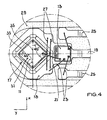
- the optoelectronic receiver shown in FIGS. 1 to 4 has a silicon photodiode 11 serving as a photosensitive semiconductor component and a control circuit 13 which are arranged, for example glued, on a ground conductor strip 15 made of metal.
- the ground conductor strip 15 has a trough-shaped recess 17 into which the photodiode 11 is inserted.
- At the opposite end of the recess 17 of the ground conductor strip 15 is formed as a ground terminal pin 19.
- the photodiode 11 and the control circuit 13 are connected to each other by means of a signal bonding wire 21, wherein the photodiode 11 and the control circuit 13 are configured such that the signal bonding wire 21 is used to transmit the received signals of the photodiode 11 to the control circuit 13.
- connection legs 25 can serve, for example, to supply the receiver with the operating voltage, while the other connection leg 25 serves as a signal output.
- two shielding bonding wires 27 are provided, which are respectively connected at both ends to the ground conductor strip 15 and which cross the signal bonding wire 21.
- the two shielding bonding wires 27 extend in the plan view according to FIGS. 2 and 4 obliquely to the signal bonding wire 21 and parallel to each other.
- connection pins 19, 25 protrude from the housing.
- the free ends of the connection legs 19, 25 run parallel to one another along a direction Y.
- the housing 29 is transparent in the infrared spectral range, for which the photodiode 11 is also sensitive.
- the light entry surface 31 of the photodiode 11 has a square shape.
- the light entry surface 31 extends within the plane which is spanned by the three free ends of the connection legs 19, 25.
- the four side edges of the square light entry surface 31 are rotated with respect to the extension direction Y of the free ends of the connection legs 19, 25 by an angle of 45 °.
- one diagonal 33 of the square light entrance surface 31 is exactly parallel to the extension direction Y of the free ends of the terminal legs 19, 25, while the other diagonal 35 of the light entry surface 31 is parallel to a direction X which is perpendicular to the direction Y.
- the optoelectronic receiver shown in FIGS. 1 to 4 serves as a signal receiver of an infrared remote control.
- the photodiode 11 converts the optical signals received in the infrared into electrical signals, which are first forwarded to the control circuit 13 via the signal bonding wire 21.
- the thus preprocessed received signals are output via a terminal pin 25 of the receiver.
- the extension direction Y of the free ends of the connection legs 19, 25 usually indicates the alignment of the shown receiver during its mounting, for example on a circuit board of an electrical appliance.
- the receiver is mounted with either horizontal or vertical alignment of the leads 19, 25. Due to the explained, rotated by 45 ° arrangement of the light entry surface 31 of the photodiode 11, the receiver has a comparatively high sensitivity in both cases with respect to the horizontal plane and the vertical plane, since the diagonal 33, 35 of the light entry surface 31 - and not the shorter side edges - parallel to the horizontal or vertical run.
- the high sensitivity with respect to the horizontal and vertical is achieved with a relatively small in area and thus cost photodiode 11, and the receiver with the housing 29 may ultimately have a relatively small size.
- the shielding bonding wires 27 effect an advantageous shielding of the signal bonding wire 21 against electromagnetic interference signals, since the shielding bonding wires 27 together with the grounding conductor strip 15 form a closed envelope of the signal bonding wire 21.
- the ground conductor strip 15 is set to the electrical ground potential of the receiver during operation of the optoelectronic receiver. Due to the The signal bonding wire 21 overlaps the shielding bonding wires 27, which are likewise set to the ground potential, to shield external electromagnetic interference signals which would otherwise be superimposed on the useful signal propagated along the signal bonding wire 21 without weakening.
- the photodiode 11 Since the photodiode 11 is rotated with respect to the extension direction Y of the connection pins 19, 25 by an angle of 45 ° and the photodiode 11 thus has a corner of its square shape in the direction of the control circuit 13, the signal bonding wire 21 on the part of the photodiode 11 at a corner region of the light entry surface 31 are attached. As a result, it is particularly easy to tension the shielding bonding wires 27 via the signal bonding wire 21 and nevertheless to connect them to the ground conductor strip 15 at both ends. For this purpose, the shielding bonding wires 27 only have to overlap the relevant corner region of the photodiode 11 or the light entry surface 31, as can be seen in particular from the plan view according to FIG. 4.
- the described shielding measure can be realized in a very simple manner in terms of production, since bonding wires 21, 23 have to be attached anyway in the production of the receiver.
- the additional attachment of the shielding bonding wires 27 on the other hand means no significant additional effort.
- Another measure for shielding the photodiode 11 against external electromagnetic interference is the arrangement of the photodiode 11 in the trough-like recess 17 of the ground conductor strip 15.
- the bottom and the side walls of the trough-shaped recess 17 suppress the incident from below and from the side of interference or at least weaken it.
- Another advantage of the arrangement of Photodiode 11 in the trough-shaped depression 17 is that the signal bonding wire 21 can take a flat course from the photodiode 11 to the control circuit 13, so that the spreading of the signal bonding wire 21 by means of the shielding bonding wires 27 is further simplified.
- FIGS. 1 to 4 also show the following advantageous development:
- the housing 29 has a substantially cuboid base body 37, in which the photodiode 11, the control circuit 13 and the terminal pins 19, 25 are encapsulated, wherein an additional lens portion 39 of the housing 29 is integrally formed on the upper side of the base body 37.
- the lens section 39 forms at a first, the front side of the receiver facing portion I of the photodiode 11, an elevation 41 of the housing 29 with respect to the light entrance surface 31.
- the lens portion 39 extends - with respect to the light entry surface 31 - constant height and thus parallel to the extension direction Y of the connection pins 19, 25 to the back of the receiver, at which the free ends of the connection pins 19, 25 protrude from the housing 29 (see side view of FIG.
- the housing 29 with the illustrated elongate lens section 39 can be produced particularly easily by a casting method, since the receiver can be pulled out of the mold ahead of the casting mold parallel to the direction Y with the connection legs 19, 25 after the casting process.
- the casting tool may have a particularly simple structure, since the height of the lens section 39 with respect to the plane of extent of the light entry surface 31 and the connection pins 19, 25 at the back of the receiver, ie in the vicinity of the free Ends of the connection pins 19, 25, not reduced again (see side view of FIG.
- the lens portion 39 for the 45 ° -rotated photodiode 11 causes a sufficient lensing effect, i. a sufficient focusing of the incident radiation on the photodiode 11:
- the lens portion 39 is namely at the said first region I of the photodiode 11 along a cross-sectional plane which is perpendicular to the light entrance surface 31 and parallel to the extension direction Y of the connection pins 19, 25 (paper plane of Side view according to FIG. 1), convexly curved.
- the lens portion 39 is also convexly curved in all regions I, II of the photodiode 11 along a cross-sectional plane that is perpendicular to the light entrance surface 31 and perpendicular to the extension direction Y of the terminal pins 19, 25 (paper plane of the front view of FIG. 3).
- a cross-sectional plane that is perpendicular to the light entrance surface 31 and perpendicular to the extension direction Y of the terminal pins 19, 25 (paper plane of the front view of FIG. 3).
- the lens section 39 on the first region I of the photodiode 11 has the shape of a spherical segment (segment angle of 90 °). Subsequently, that is, from the second region II of the photodiode 11, the lens section 39 is in the form of a cylinder segment (semi-cylindrical shape), whose longitudinal axis is parallel to the direction Y.
- Fig. 5 shows that the illustrated trough-shaped recess 17 of the ground conductor strip 15 is not mandatory.
- the photodiode 11 and the control circuit 13 are instead arranged at the same height on the ground conductor strip 15.
Landscapes
- Light Receiving Elements (AREA)
- Polysaccharides And Polysaccharide Derivatives (AREA)
- Optical Communication System (AREA)
- Absorbent Articles And Supports Therefor (AREA)
Claims (11)
- Récepteur optoélectronique, en particulier module récepteur de télécommande, comprenant un composant semi-conducteur photosensible (11), plusieurs pattes de raccordement (19, 25) et un boîtier (29),
dans lequel le composant semi-conducteur photosensible (11) et les pattes de raccordement (19, 25) sont intégrés par coulée dans le boîtier (29) de telle manière que les pattes de raccordement dépassent hors du boîtier par une extrémité libre respective, et
dans lequel la surface d'entrée de lumière (31) du composant semi-conducteur photosensible (11) possède une forme sensiblement rectangulaire,
caractérisé en ce que
les arêtes latérales de la surface d'entrée de lumière (31) du composant semi-conducteur photosensible (11) font un angle de 45° par rapport à la direction d'extension des extrémités libres des pattes de raccordement (19, 25). - Récepteur optoélectronique selon la revendication 1, caractérisé en ce que la surface d'entrée de lumière (31) du composant semi-conducteur photosensible (11) possède une forme sensiblement carrée.
- Récepteur optoélectronique selon l'une des revendications précédentes, caractérisé en ce que la surface d'entrée de lumière (31) du composant semi-conducteur photosensible (11) s'étend à l'intérieur d'un plan qui est parallèle au plan défini par les extrémités libres des pattes de raccordement (19, 25).
- Récepteur optoélectronique selon l'une des revendications précédentes, caractérisé en ce que le boîtier (29) présente une portion en lentille (39) qui forme au niveau d'une première zone (I) du composant semi-conducteur photosensible (11) une surélévation (41) du boîtier, et qui s'étend, à partir d'une deuxième zone successive (II) du composant semi-conducteur photosensible, à une hauteur qui reste constante par rapport à la surface d'entrée de lumière (31) du composant semi-conducteur photosensible (11).
- Récepteur optoélectronique selon la revendication 4, caractérisé en ce que la portion en lentille (39) du boîtier (29) s'étend à partir de la seconde zone (II) du composant semi-conducteur photosensible (11) jusqu'au côté du récepteur au niveau duquel les pattes de raccordement (19, 25) dépassent hors du boîtier.
- Récepteur optoélectronique selon l'une des revendications 4 ou 5, caractérisé en ce que la portion en lentille (39) du boîtier (29) est cintrée sous forme convexe au niveau de la première zone (I) du composant semi-conducteur photosensible (11) le long d'un plan de section transversale qui s'étend perpendiculairement à la surface d'entrée de lumière (31) du composant semi-conducteur photosensible (11) et parallèlement à la direction d'extension des extrémités libres des pattes de raccordement (19, 25),
et/ou
en ce que la portion en lentille (39) est cintrée sous forme convexe le long d'un plan de section transversale qui s'étend perpendiculairement à la surface d'entrée de lumière (31) du composant semi-conducteur photosensible (11) et perpendiculairement à la direction d'extension des extrémités libres des pattes de raccordement (19, 25). - Récepteur optoélectronique selon l'une des revendications 4 à 6, caractérisé en ce que la portion en lentille (39) du boîtier (29) possède, au niveau de la première zone (I) du composant semi-conducteur photosensible (11), la forme d'un segment de sphère, et en ce que la portion en lentille (39) se transforme ensuite à partir de la seconde zone (II) du composant semi-conducteur photosensible (11) en une forme d'un segment de cylindre, dont l'axe longitudinal s'étend parallèlement à la direction d'extension des extrémités libres des pattes de raccordement (19, 25).
- Récepteur optoélectronique selon l'une des revendications 4 à 7, caractérisé en ce que le boîtier (29) présente un corps de base (37) de forme parallélépipédique dans lequel le composant semi-conducteur photosensible (11) et les pattes de raccordement (19,25) sont intégrés par coulée, la portion en lentille (39) étant conformée sur le corps de base (37).
- Récepteur optoélectronique selon l'une des revendications précédentes, caractérisé en ce que le récepteur optoélectronique comprend additionnellement un circuit de commande (13), ledit composant semi-conducteur photosensible (11) étant raccordé au circuit de commande pour transmettre des signaux reçus au moyen d'une ligne à signaux (21), et en ce que le récepteur optoélectronique comporte au moins un fil de bonding de blindage (27) qui s'étend transversalement à la ligne à signaux (21), qui coiffe la ligne à signaux, et qui est relié aux deux extrémités à un raccord à potentiel constant (15).
- Récepteur optoélectronique selon la revendication 9, caractérisé en ce que le fils de bonding de blindage (27) forme avec le raccord à potentiel constant (15) une boucle fermée qui entoure la ligne à signaux (21),
et/ou
en ce que le fil de bonding de blindage (27) est relié aux deux extrémités à une bande conductrice de masse (15). - Récepteur optoélectronique selon l'une des revendications précédentes, caractérisé en ce qu'un renfoncement en forme de cuvette (17) est formé sur la bande conductrice de masse (15), et en ce que le composant semi-conducteur photosensible (11) est agencé dans le renfoncement.
Priority Applications (6)
| Application Number | Priority Date | Filing Date | Title |
|---|---|---|---|
| PL04010490T PL1594167T3 (pl) | 2004-05-03 | 2004-05-03 | Odbiornik optoelektroniczny |
| DE502004002673T DE502004002673D1 (de) | 2004-05-03 | 2004-05-03 | Optoelektronischer Empfänger |
| EP04010490A EP1594167B1 (fr) | 2004-05-03 | 2004-05-03 | Récepteur optoélectronique |
| AT04010490T ATE352102T1 (de) | 2004-05-03 | 2004-05-03 | Optoelektronischer empfänger |
| PCT/EP2005/004592 WO2005109523A1 (fr) | 2004-05-03 | 2005-04-28 | Recepteur optoelectronique |
| TW094114088A TWI379420B (en) | 2004-05-03 | 2005-05-02 | An optoelectronic receiver |
Applications Claiming Priority (1)
| Application Number | Priority Date | Filing Date | Title |
|---|---|---|---|
| EP04010490A EP1594167B1 (fr) | 2004-05-03 | 2004-05-03 | Récepteur optoélectronique |
Publications (2)
| Publication Number | Publication Date |
|---|---|
| EP1594167A1 EP1594167A1 (fr) | 2005-11-09 |
| EP1594167B1 true EP1594167B1 (fr) | 2007-01-17 |
Family
ID=34924836
Family Applications (1)
| Application Number | Title | Priority Date | Filing Date |
|---|---|---|---|
| EP04010490A Expired - Lifetime EP1594167B1 (fr) | 2004-05-03 | 2004-05-03 | Récepteur optoélectronique |
Country Status (6)
| Country | Link |
|---|---|
| EP (1) | EP1594167B1 (fr) |
| AT (1) | ATE352102T1 (fr) |
| DE (1) | DE502004002673D1 (fr) |
| PL (1) | PL1594167T3 (fr) |
| TW (1) | TWI379420B (fr) |
| WO (1) | WO2005109523A1 (fr) |
Cited By (1)
| Publication number | Priority date | Publication date | Assignee | Title |
|---|---|---|---|---|
| WO2025149375A1 (fr) * | 2024-01-09 | 2025-07-17 | Robert Bosch Gmbh | Dispositif microcapteur comprenant au moins un fil de connexion supplémentaire dans une masse de protection |
Families Citing this family (1)
| Publication number | Priority date | Publication date | Assignee | Title |
|---|---|---|---|---|
| TWI553817B (zh) | 2014-06-17 | 2016-10-11 | 瑞昱半導體股份有限公司 | 具有電磁防護功能之積體電路及其製造方法 |
Family Cites Families (4)
| Publication number | Priority date | Publication date | Assignee | Title |
|---|---|---|---|---|
| DE4212948A1 (de) * | 1992-04-18 | 1993-10-21 | Telefunken Microelectron | Halbleiterbaugruppe, insbesondere Fernsteuer-Empfangsmodul |
| US5416871A (en) * | 1993-04-09 | 1995-05-16 | Sumitomo Electric Industries, Ltd. | Molded optical connector module |
| JP3601076B2 (ja) * | 1994-06-14 | 2004-12-15 | ソニー株式会社 | 受光装置 |
| US5763900A (en) * | 1996-12-05 | 1998-06-09 | Taiwan Liton Electronic Co. Ltd. | Infrared transceiver package |
-
2004
- 2004-05-03 AT AT04010490T patent/ATE352102T1/de not_active IP Right Cessation
- 2004-05-03 EP EP04010490A patent/EP1594167B1/fr not_active Expired - Lifetime
- 2004-05-03 PL PL04010490T patent/PL1594167T3/pl unknown
- 2004-05-03 DE DE502004002673T patent/DE502004002673D1/de not_active Expired - Lifetime
-
2005
- 2005-04-28 WO PCT/EP2005/004592 patent/WO2005109523A1/fr not_active Ceased
- 2005-05-02 TW TW094114088A patent/TWI379420B/zh not_active IP Right Cessation
Cited By (1)
| Publication number | Priority date | Publication date | Assignee | Title |
|---|---|---|---|---|
| WO2025149375A1 (fr) * | 2024-01-09 | 2025-07-17 | Robert Bosch Gmbh | Dispositif microcapteur comprenant au moins un fil de connexion supplémentaire dans une masse de protection |
Also Published As
| Publication number | Publication date |
|---|---|
| TWI379420B (en) | 2012-12-11 |
| EP1594167A1 (fr) | 2005-11-09 |
| TW200605366A (en) | 2006-02-01 |
| DE502004002673D1 (de) | 2007-03-08 |
| WO2005109523A1 (fr) | 2005-11-17 |
| PL1594167T3 (pl) | 2007-06-29 |
| ATE352102T1 (de) | 2007-02-15 |
Similar Documents
| Publication | Publication Date | Title |
|---|---|---|
| EP1174745B1 (fr) | Module optoélectronique montable en surface | |
| EP1252540B1 (fr) | Module emetteur et/ou recepteur optique muni d'un guide d'ondes lumineuses interieur | |
| DE69114161T2 (de) | Optoelektronische Baugruppe. | |
| DE69220613T2 (de) | Gegossene optische Modulanordnung | |
| DE69118497T2 (de) | Kamerakopf für eine Festkörper-Bildaufnahme-Einrichtung und Verfahren zur Herstellung | |
| EP1695037B1 (fr) | Procede pour produire un appareil de commutation, et composant pour cet appareil de commutation | |
| EP2614396A2 (fr) | Composant optoélectronique | |
| WO2012031780A2 (fr) | Composant opto-électronique | |
| WO2003076998A1 (fr) | Module optoelectronique et ensemble fiche male | |
| DE212015000174U1 (de) | Ein Optokoppler und dessen Komponenten | |
| EP1483613B1 (fr) | Partie de reception et de couplage pour un element emetteur optoelectronique | |
| EP1594167B1 (fr) | Récepteur optoélectronique | |
| DE60213083T2 (de) | Vorrichtung zum anordnen eines photoelektrischen wandlers auf einem elektrischen signalverarbeitungsgerät | |
| DE112010002553T5 (de) | Modul zur optischen kommunikation | |
| EP1591813B1 (fr) | Méthode d'alignement d'un guide d'onde optique avec une unitée optique comprenant un module optique, module optique et jeu de construction comprenant un module optique | |
| EP1623256B1 (fr) | Module micro-optique pourvu d'un boitier moule par injection et procedes de fabrication dudit module | |
| DE102015102717A1 (de) | Ausgeformte Leiterrahmen für eine Leiterplatte-zu-Leiterplatte-Verbindung | |
| DE10158132A1 (de) | Photosensorvorrichtung und Verfahren zu ihrer Herstellung | |
| EP1608026A2 (fr) | Dispositif optoélectronique et son procédé de fabrication | |
| DE10348218B4 (de) | Optisches Verbindungselement | |
| DE102006012780B3 (de) | Optokoppler zur Übertragung von optischen in elektrische Signale und umgekehrt | |
| DE102006062279B4 (de) | MID-Modul und Verfahren zur Montage einer optischen Faser in einem MID-Modul | |
| EP4464988B1 (fr) | Capteur avec boîtier et câble | |
| DE102015107339A1 (de) | Eine als oberflächenbestückte Einrichtung (SMD) ausgebildete optische Anschlussvorrichtung | |
| DE19714970C2 (de) | Koppelelement für Lichtwellenleiterkabel |
Legal Events
| Date | Code | Title | Description |
|---|---|---|---|
| PUAI | Public reference made under article 153(3) epc to a published international application that has entered the european phase |
Free format text: ORIGINAL CODE: 0009012 |
|
| AK | Designated contracting states |
Kind code of ref document: A1 Designated state(s): AT BE BG CH CY CZ DE DK EE ES FI FR GB GR HU IE IT LI LU MC NL PL PT RO SE SI SK TR |
|
| AX | Request for extension of the european patent |
Extension state: AL HR LT LV MK |
|
| 17P | Request for examination filed |
Effective date: 20060118 |
|
| AKX | Designation fees paid |
Designated state(s): AT BE BG CH CY CZ DE DK EE ES FI FR GB GR HU IE IT LI LU MC NL PL PT RO SE SI SK TR |
|
| GRAP | Despatch of communication of intention to grant a patent |
Free format text: ORIGINAL CODE: EPIDOSNIGR1 |
|
| GRAS | Grant fee paid |
Free format text: ORIGINAL CODE: EPIDOSNIGR3 |
|
| GRAA | (expected) grant |
Free format text: ORIGINAL CODE: 0009210 |
|
| AK | Designated contracting states |
Kind code of ref document: B1 Designated state(s): AT BE BG CH CY CZ DE DK EE ES FI FR GB GR HU IE IT LI LU MC NL PL PT RO SE SI SK TR |
|
| PG25 | Lapsed in a contracting state [announced via postgrant information from national office to epo] |
Ref country code: DK Free format text: LAPSE BECAUSE OF FAILURE TO SUBMIT A TRANSLATION OF THE DESCRIPTION OR TO PAY THE FEE WITHIN THE PRESCRIBED TIME-LIMIT Effective date: 20070117 Ref country code: IE Free format text: LAPSE BECAUSE OF FAILURE TO SUBMIT A TRANSLATION OF THE DESCRIPTION OR TO PAY THE FEE WITHIN THE PRESCRIBED TIME-LIMIT Effective date: 20070117 Ref country code: SI Free format text: LAPSE BECAUSE OF FAILURE TO SUBMIT A TRANSLATION OF THE DESCRIPTION OR TO PAY THE FEE WITHIN THE PRESCRIBED TIME-LIMIT Effective date: 20070117 Ref country code: NL Free format text: LAPSE BECAUSE OF FAILURE TO SUBMIT A TRANSLATION OF THE DESCRIPTION OR TO PAY THE FEE WITHIN THE PRESCRIBED TIME-LIMIT Effective date: 20070117 Ref country code: FI Free format text: LAPSE BECAUSE OF FAILURE TO SUBMIT A TRANSLATION OF THE DESCRIPTION OR TO PAY THE FEE WITHIN THE PRESCRIBED TIME-LIMIT Effective date: 20070117 |
|
| REG | Reference to a national code |
Ref country code: GB Ref legal event code: FG4D Free format text: NOT ENGLISH |
|
| REG | Reference to a national code |
Ref country code: CH Ref legal event code: EP |
|
| REG | Reference to a national code |
Ref country code: IE Ref legal event code: FG4D Free format text: LANGUAGE OF EP DOCUMENT: GERMAN |
|
| REF | Corresponds to: |
Ref document number: 502004002673 Country of ref document: DE Date of ref document: 20070308 Kind code of ref document: P |
|
| PG25 | Lapsed in a contracting state [announced via postgrant information from national office to epo] |
Ref country code: SE Free format text: LAPSE BECAUSE OF FAILURE TO SUBMIT A TRANSLATION OF THE DESCRIPTION OR TO PAY THE FEE WITHIN THE PRESCRIBED TIME-LIMIT Effective date: 20070417 |
|
| PG25 | Lapsed in a contracting state [announced via postgrant information from national office to epo] |
Ref country code: BG Free format text: LAPSE BECAUSE OF FAILURE TO SUBMIT A TRANSLATION OF THE DESCRIPTION OR TO PAY THE FEE WITHIN THE PRESCRIBED TIME-LIMIT Effective date: 20070418 |
|
| PG25 | Lapsed in a contracting state [announced via postgrant information from national office to epo] |
Ref country code: ES Free format text: LAPSE BECAUSE OF FAILURE TO SUBMIT A TRANSLATION OF THE DESCRIPTION OR TO PAY THE FEE WITHIN THE PRESCRIBED TIME-LIMIT Effective date: 20070428 |
|
| GBT | Gb: translation of ep patent filed (gb section 77(6)(a)/1977) |
Effective date: 20070416 |
|
| PG25 | Lapsed in a contracting state [announced via postgrant information from national office to epo] |
Ref country code: PT Free format text: LAPSE BECAUSE OF FAILURE TO SUBMIT A TRANSLATION OF THE DESCRIPTION OR TO PAY THE FEE WITHIN THE PRESCRIBED TIME-LIMIT Effective date: 20070618 |
|
| REG | Reference to a national code |
Ref country code: PL Ref legal event code: T3 |
|
| NLV1 | Nl: lapsed or annulled due to failure to fulfill the requirements of art. 29p and 29m of the patents act | ||
| ET | Fr: translation filed | ||
| REG | Reference to a national code |
Ref country code: IE Ref legal event code: FD4D |
|
| PLBE | No opposition filed within time limit |
Free format text: ORIGINAL CODE: 0009261 |
|
| STAA | Information on the status of an ep patent application or granted ep patent |
Free format text: STATUS: NO OPPOSITION FILED WITHIN TIME LIMIT |
|
| PG25 | Lapsed in a contracting state [announced via postgrant information from national office to epo] |
Ref country code: SK Free format text: LAPSE BECAUSE OF FAILURE TO SUBMIT A TRANSLATION OF THE DESCRIPTION OR TO PAY THE FEE WITHIN THE PRESCRIBED TIME-LIMIT Effective date: 20070117 |
|
| 26N | No opposition filed |
Effective date: 20071018 |
|
| BERE | Be: lapsed |
Owner name: VISHAY SEMICONDUCTOR G.M.B.H. Effective date: 20070531 |
|
| PG25 | Lapsed in a contracting state [announced via postgrant information from national office to epo] |
Ref country code: CZ Free format text: LAPSE BECAUSE OF FAILURE TO SUBMIT A TRANSLATION OF THE DESCRIPTION OR TO PAY THE FEE WITHIN THE PRESCRIBED TIME-LIMIT Effective date: 20070117 Ref country code: RO Free format text: LAPSE BECAUSE OF FAILURE TO SUBMIT A TRANSLATION OF THE DESCRIPTION OR TO PAY THE FEE WITHIN THE PRESCRIBED TIME-LIMIT Effective date: 20070117 |
|
| PG25 | Lapsed in a contracting state [announced via postgrant information from national office to epo] |
Ref country code: MC Free format text: LAPSE BECAUSE OF NON-PAYMENT OF DUE FEES Effective date: 20070531 |
|
| PG25 | Lapsed in a contracting state [announced via postgrant information from national office to epo] |
Ref country code: BE Free format text: LAPSE BECAUSE OF NON-PAYMENT OF DUE FEES Effective date: 20070531 |
|
| PG25 | Lapsed in a contracting state [announced via postgrant information from national office to epo] |
Ref country code: GR Free format text: LAPSE BECAUSE OF FAILURE TO SUBMIT A TRANSLATION OF THE DESCRIPTION OR TO PAY THE FEE WITHIN THE PRESCRIBED TIME-LIMIT Effective date: 20070418 |
|
| PG25 | Lapsed in a contracting state [announced via postgrant information from national office to epo] |
Ref country code: AT Free format text: LAPSE BECAUSE OF NON-PAYMENT OF DUE FEES Effective date: 20070503 |
|
| REG | Reference to a national code |
Ref country code: CH Ref legal event code: PL |
|
| PG25 | Lapsed in a contracting state [announced via postgrant information from national office to epo] |
Ref country code: EE Free format text: LAPSE BECAUSE OF FAILURE TO SUBMIT A TRANSLATION OF THE DESCRIPTION OR TO PAY THE FEE WITHIN THE PRESCRIBED TIME-LIMIT Effective date: 20070117 Ref country code: CH Free format text: LAPSE BECAUSE OF NON-PAYMENT OF DUE FEES Effective date: 20080531 Ref country code: LI Free format text: LAPSE BECAUSE OF NON-PAYMENT OF DUE FEES Effective date: 20080531 |
|
| PG25 | Lapsed in a contracting state [announced via postgrant information from national office to epo] |
Ref country code: CY Free format text: LAPSE BECAUSE OF FAILURE TO SUBMIT A TRANSLATION OF THE DESCRIPTION OR TO PAY THE FEE WITHIN THE PRESCRIBED TIME-LIMIT Effective date: 20070117 |
|
| PG25 | Lapsed in a contracting state [announced via postgrant information from national office to epo] |
Ref country code: LU Free format text: LAPSE BECAUSE OF NON-PAYMENT OF DUE FEES Effective date: 20070503 |
|
| PG25 | Lapsed in a contracting state [announced via postgrant information from national office to epo] |
Ref country code: HU Free format text: LAPSE BECAUSE OF FAILURE TO SUBMIT A TRANSLATION OF THE DESCRIPTION OR TO PAY THE FEE WITHIN THE PRESCRIBED TIME-LIMIT Effective date: 20070718 |
|
| REG | Reference to a national code |
Ref country code: FR Ref legal event code: PLFP Year of fee payment: 13 |
|
| REG | Reference to a national code |
Ref country code: FR Ref legal event code: PLFP Year of fee payment: 14 |
|
| REG | Reference to a national code |
Ref country code: FR Ref legal event code: PLFP Year of fee payment: 15 |
|
| PGFP | Annual fee paid to national office [announced via postgrant information from national office to epo] |
Ref country code: IT Payment date: 20230526 Year of fee payment: 20 Ref country code: FR Payment date: 20230525 Year of fee payment: 20 Ref country code: DE Payment date: 20230519 Year of fee payment: 20 |
|
| PGFP | Annual fee paid to national office [announced via postgrant information from national office to epo] |
Ref country code: TR Payment date: 20230502 Year of fee payment: 20 Ref country code: PL Payment date: 20230421 Year of fee payment: 20 |
|
| PGFP | Annual fee paid to national office [announced via postgrant information from national office to epo] |
Ref country code: GB Payment date: 20230522 Year of fee payment: 20 |
|
| REG | Reference to a national code |
Ref country code: DE Ref legal event code: R071 Ref document number: 502004002673 Country of ref document: DE |
|
| REG | Reference to a national code |
Ref country code: GB Ref legal event code: PE20 Expiry date: 20240502 |
|
| PG25 | Lapsed in a contracting state [announced via postgrant information from national office to epo] |
Ref country code: GB Free format text: LAPSE BECAUSE OF EXPIRATION OF PROTECTION Effective date: 20240502 |
|
| PG25 | Lapsed in a contracting state [announced via postgrant information from national office to epo] |
Ref country code: GB Free format text: LAPSE BECAUSE OF EXPIRATION OF PROTECTION Effective date: 20240502 |