EP1594128B1 - Optisches Element, Objektiv-System, optische Abtastvorrichtung, und optisches Plattenlaufwerk - Google Patents
Optisches Element, Objektiv-System, optische Abtastvorrichtung, und optisches Plattenlaufwerk Download PDFInfo
- Publication number
- EP1594128B1 EP1594128B1 EP05252748A EP05252748A EP1594128B1 EP 1594128 B1 EP1594128 B1 EP 1594128B1 EP 05252748 A EP05252748 A EP 05252748A EP 05252748 A EP05252748 A EP 05252748A EP 1594128 B1 EP1594128 B1 EP 1594128B1
- Authority
- EP
- European Patent Office
- Prior art keywords
- optical
- light
- light flux
- area
- optical element
- Prior art date
- Legal status (The legal status is an assumption and is not a legal conclusion. Google has not performed a legal analysis and makes no representation as to the accuracy of the status listed.)
- Expired - Lifetime
Links
- 230000003287 optical effect Effects 0.000 title claims abstract description 249
- 230000004907 flux Effects 0.000 claims abstract description 159
- 230000004075 alteration Effects 0.000 claims description 34
- 230000014509 gene expression Effects 0.000 claims description 21
- 239000011241 protective layer Substances 0.000 claims description 20
- 239000011347 resin Substances 0.000 claims description 13
- 229920005989 resin Polymers 0.000 claims description 13
- 239000010410 layer Substances 0.000 claims description 9
- 239000011521 glass Substances 0.000 claims description 5
- 239000000758 substrate Substances 0.000 claims description 4
- 244000154870 Viola adunca Species 0.000 description 16
- 235000005811 Viola adunca Nutrition 0.000 description 16
- 235000013487 Viola odorata Nutrition 0.000 description 16
- 235000002254 Viola papilionacea Nutrition 0.000 description 16
- 230000009471 action Effects 0.000 description 14
- 239000004065 semiconductor Substances 0.000 description 13
- 101150099000 EXPA1 gene Proteins 0.000 description 11
- 102100029095 Exportin-1 Human genes 0.000 description 11
- 101100119348 Saccharomyces cerevisiae (strain ATCC 204508 / S288c) EXP1 gene Proteins 0.000 description 11
- 101100269618 Streptococcus pneumoniae serotype 4 (strain ATCC BAA-334 / TIGR4) aliA gene Proteins 0.000 description 11
- 108700002148 exportin 1 Proteins 0.000 description 11
- 230000008859 change Effects 0.000 description 10
- 102100029091 Exportin-2 Human genes 0.000 description 8
- 101710147878 Exportin-2 Proteins 0.000 description 8
- 239000004973 liquid crystal related substance Substances 0.000 description 5
- 238000004519 manufacturing process Methods 0.000 description 5
- 101100328890 Arabidopsis thaliana COL3 gene Proteins 0.000 description 4
- 201000009310 astigmatism Diseases 0.000 description 4
- 101100328883 Arabidopsis thaliana COL1 gene Proteins 0.000 description 3
- 101100328886 Caenorhabditis elegans col-2 gene Proteins 0.000 description 3
- 230000005540 biological transmission Effects 0.000 description 3
- 239000006185 dispersion Substances 0.000 description 3
- 238000000034 method Methods 0.000 description 3
- 238000009826 distribution Methods 0.000 description 2
- 239000005304 optical glass Substances 0.000 description 2
- 230000010355 oscillation Effects 0.000 description 2
- 210000001747 pupil Anatomy 0.000 description 2
- 230000001105 regulatory effect Effects 0.000 description 2
- 238000005549 size reduction Methods 0.000 description 2
- 230000007480 spreading Effects 0.000 description 2
- 238000003892 spreading Methods 0.000 description 2
- 241001025261 Neoraja caerulea Species 0.000 description 1
- 230000008901 benefit Effects 0.000 description 1
- 238000006243 chemical reaction Methods 0.000 description 1
- 230000001276 controlling effect Effects 0.000 description 1
- 230000000694 effects Effects 0.000 description 1
- 239000000463 material Substances 0.000 description 1
- 230000000737 periodic effect Effects 0.000 description 1
- 230000002093 peripheral effect Effects 0.000 description 1
- 230000001681 protective effect Effects 0.000 description 1
- 230000009467 reduction Effects 0.000 description 1
- 238000004904 shortening Methods 0.000 description 1
Images

Classifications
-
- G—PHYSICS
- G11—INFORMATION STORAGE
- G11B—INFORMATION STORAGE BASED ON RELATIVE MOVEMENT BETWEEN RECORD CARRIER AND TRANSDUCER
- G11B7/00—Recording or reproducing by optical means, e.g. recording using a thermal beam of optical radiation by modifying optical properties or the physical structure, reproducing using an optical beam at lower power by sensing optical properties; Record carriers therefor
- G11B7/12—Heads, e.g. forming of the optical beam spot or modulation of the optical beam
- G11B7/135—Means for guiding the beam from the source to the record carrier or from the record carrier to the detector
- G11B7/1392—Means for controlling the beam wavefront, e.g. for correction of aberration
- G11B7/13922—Means for controlling the beam wavefront, e.g. for correction of aberration passive
-
- G—PHYSICS
- G02—OPTICS
- G02B—OPTICAL ELEMENTS, SYSTEMS OR APPARATUS
- G02B5/00—Optical elements other than lenses
- G02B5/18—Diffraction gratings
-
- G—PHYSICS
- G11—INFORMATION STORAGE
- G11B—INFORMATION STORAGE BASED ON RELATIVE MOVEMENT BETWEEN RECORD CARRIER AND TRANSDUCER
- G11B7/00—Recording or reproducing by optical means, e.g. recording using a thermal beam of optical radiation by modifying optical properties or the physical structure, reproducing using an optical beam at lower power by sensing optical properties; Record carriers therefor
- G11B7/12—Heads, e.g. forming of the optical beam spot or modulation of the optical beam
- G11B7/135—Means for guiding the beam from the source to the record carrier or from the record carrier to the detector
- G11B7/1353—Diffractive elements, e.g. holograms or gratings
-
- G—PHYSICS
- G11—INFORMATION STORAGE
- G11B—INFORMATION STORAGE BASED ON RELATIVE MOVEMENT BETWEEN RECORD CARRIER AND TRANSDUCER
- G11B7/00—Recording or reproducing by optical means, e.g. recording using a thermal beam of optical radiation by modifying optical properties or the physical structure, reproducing using an optical beam at lower power by sensing optical properties; Record carriers therefor
- G11B7/12—Heads, e.g. forming of the optical beam spot or modulation of the optical beam
- G11B7/135—Means for guiding the beam from the source to the record carrier or from the record carrier to the detector
- G11B7/1365—Separate or integrated refractive elements, e.g. wave plates
- G11B7/1369—Active plates, e.g. liquid crystal panels or electrostrictive elements
-
- G—PHYSICS
- G11—INFORMATION STORAGE
- G11B—INFORMATION STORAGE BASED ON RELATIVE MOVEMENT BETWEEN RECORD CARRIER AND TRANSDUCER
- G11B7/00—Recording or reproducing by optical means, e.g. recording using a thermal beam of optical radiation by modifying optical properties or the physical structure, reproducing using an optical beam at lower power by sensing optical properties; Record carriers therefor
- G11B7/12—Heads, e.g. forming of the optical beam spot or modulation of the optical beam
- G11B7/135—Means for guiding the beam from the source to the record carrier or from the record carrier to the detector
- G11B7/1372—Lenses
- G11B7/1374—Objective lenses
-
- G—PHYSICS
- G11—INFORMATION STORAGE
- G11B—INFORMATION STORAGE BASED ON RELATIVE MOVEMENT BETWEEN RECORD CARRIER AND TRANSDUCER
- G11B7/00—Recording or reproducing by optical means, e.g. recording using a thermal beam of optical radiation by modifying optical properties or the physical structure, reproducing using an optical beam at lower power by sensing optical properties; Record carriers therefor
- G11B7/12—Heads, e.g. forming of the optical beam spot or modulation of the optical beam
- G11B7/135—Means for guiding the beam from the source to the record carrier or from the record carrier to the detector
- G11B7/139—Numerical aperture control means
-
- G—PHYSICS
- G11—INFORMATION STORAGE
- G11B—INFORMATION STORAGE BASED ON RELATIVE MOVEMENT BETWEEN RECORD CARRIER AND TRANSDUCER
- G11B7/00—Recording or reproducing by optical means, e.g. recording using a thermal beam of optical radiation by modifying optical properties or the physical structure, reproducing using an optical beam at lower power by sensing optical properties; Record carriers therefor
- G11B2007/0003—Recording, reproducing or erasing systems characterised by the structure or type of the carrier
- G11B2007/0006—Recording, reproducing or erasing systems characterised by the structure or type of the carrier adapted for scanning different types of carrier, e.g. CD & DVD
Definitions
- the present invention relates to an optical element (herein after, there is a case where it is called wavelength selection element) adequate when it is used for an optical pick-up apparatus by which the recording and/or reproducing of the information can be compatibly conducted on different kinds of optical disks, an objective optical system, an optical pick-up apparatus, and a drive apparatus of optical disks.
- an optical element herein after, there is a case where it is called wavelength selection element
- the wavelength-shortening of the laser light source used as the light source for reproducing of the information recorded in an optical disk or recording of the information in the optical disk is advanced, for example, a blue violet laser light source of wavelength 400 - 420 nm such as a blue violet semiconductor laser, or a blue violet SHG laser which conducts the wavelength conversion of the infrared semiconductor laser by using the second harmonic wave, is putting to a practical use.
- a blue violet laser light source of wavelength 400 - 420 nm such as a blue violet semiconductor laser, or a blue violet SHG laser which conducts the wavelength conversion of the infrared semiconductor laser by using the second harmonic wave
- the information of 15 - 20 GB can be recorded in an optical disk of diameter 12 cm, and in the case where NA of the objective optical system is increased to 0.85, the information of 23 - 25 GB can be recorded in the optical disk of diameter 12 cm.
- NA numerical aperture
- the optical disk and photo-magnetic disk for which the blue violet laser light source is used are generally referred as "high density optical disk”.
- the optical pick-up apparatus mounted in the optical disk player/recorder for the high density optical disk has a performance by which the information can be adequately recorded/reproduced while the compatibility is being kept with also any one of optical disks of the high density optical disk, DVD and CD.
- the necessity that the numerical aperture of the objective optical system is switched during the exchange to the different optical disk is generated. It is general that the switching of the large and small numerical apertures is conducted by changing the light flux diameter, however, it is considered that, for example, the liquid crystal shutter is driven in timed relationship with the timing of switching to the different optical disk, and the diameter of the light flux passing this liquid crystal shutter is changed.
- the electric control system for controlling the liquid crystal shutter becomes necessary, and the production cost is increased.
- the light which can pass the liquid crystal shutter is only a polarized light having a predetermined oscillation direction, it is necessary that the lens design is conducted considering the oscillation direction for the purpose that the irradiation light is effectively passed, and there is also a problem that the degree of the freedom of the design work is limited.
- Patent Document 1 a diffraction type filter in which a zone plate which has the first area structuring the central part of the filter, and the second area positioned outside the central part of the filter, and the aberration correction function to only any one hand light of the light of two wavelengths ⁇ 1, ⁇ 2 which are different from each other, is formed in the first area, and the diffraction lattice which practically has the light shielding function only to one hand light of the light of 2 wavelengths ⁇ 1, ⁇ 2, is formed in the second area, is disclosed.
- a diffraction type filter in which a zone plate which has the first area structuring the central part of the filter, and the second area positioned outside the central part of the filter, and the aberration correction function to only any one hand light of the light of two wavelengths ⁇ 1, ⁇ 2 which are different from each other, is formed in the first area, and the diffraction lattice which practically has the light shielding function only to one hand light of the light of 2 wavelengths ⁇ 1, ⁇ 2, is formed in the second
- the diffraction type filter written in Patent Document 1 is a filter which corresponds to light fluxes of different 2 wavelengths, and is inadequate for the use for the optical pick-up apparatus by which the recording and/or reproducing of the information is conducted on optical disks more than 3 kinds of, for example, the high density optical disk, DVD, CD.
- WO-A-2004/012188 which is used for the two-part form delimitation
- WO-A-03/091764 and WO-A-03/060892 each disclose optical elements for optical pick-up apparatuses for use with light fluxes at three different wavelengths.
- the present invention is attained in view of the conventional problem, and the object of the present invention is to provide an optical pick-up apparatus by which, although the recording and/or reproducing of the information can be adequately conducted on different 3 kinds of optical disks, the size reduction can be intended, and a drive apparatus of the optical disk, and an objective optical system and an optical element used for it.
- the first aspect of the present invention is an optical element as defined in claim 1.
- the second aspect of the present invention is an objective optical system as defined in claim 10.
- the third aspect of the present invention is an optical pick-up apparatus as defined in claim 11.
- the fourth aspect of the present invention is a drive apparatus for an optical disk as defined in claim 13.
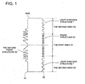
- Fig. 1 is a sectional view showing an example of an optical element (wavelength selection element).
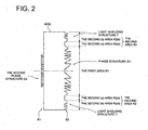
- Fig. 2 is a sectional view showing another example of an optical element (wavelength selection element).
- Fig. 3 is a view generally showing a structure of an optical pick-up apparatus PU according to the present embodiment.
- the wavelength selection element WSE generally shown in Fig. 1 , as will be described later referring to Fig. 3 , structures a light converging element CE and an objective optical system OBJ.
- the optical surface S2 of the optical disk side of the wavelength selection element WSE is divided into the first area R1 corresponding to the numerical aperture NA3 which structures a central part including the optical axis, and the second area R2 which is positioned in the outside of the first area R1, and in the first area R1, a phase structure D1 (hereinafter, there is also a case where called the first phase structure) by which the first light flux and the second light flux are not diffracted, but the third light flux is diffracted, is formed, and in the second area R2, a light-shielding structure by which the first light flux and the second light flux are transmitted, and a light-shielding structure T which is capable of substantially shielding only the third light flux, is formed.
- a phase structure D1 hereinafter, there is also a case where called the first phase structure
- a phrase "a light shielding structure being capable of substantially shielding a predetermined light flux” indicates that the predetermined light flux passing the light-shielding structure T is made not to effectively contribute to the recording and/or reproducing conducted on the optical disk.
- the light-shielding structure T for example, when the predetermined light flux passing the light-shielding structure T is diffracted, a structure in which the predetermined light flux is made not to contribute to the recording and/or reproducing on the optical disk, or by a method by which the phase is dislocated by adding the optical path difference to the predetermined light flux incident on the light-shielding structure T, when mutual light fluxes passed the convex part and the concave part of the light-shielding structure T are cancelled with each other, a structure by which they are made not so as to contribute to the recording and/or reproducing on the optical disk, are listed.
- the light-shielding structure T may be provided on the whole of the second area R2, or on a part of the second area
- a phrase that "a phase structure being capable of compensating aberration of a predetermined light flux" expresses that the phase structure has an action to reduce the aberration on the wave-front of the light conversing spot formed on the optical disk by the predetermined light flux, to the predetermined light flux passed the phase structure.
- phase structure or the light-shielding structure used in the present invention, when they have the above action, particularly they are not limited, however, a structure, in which, for example, patterns whose sectional shape including the optical axis is rectangular, are arranged concentric circularly, is listed.
- the step difference of this rectangular pattern can be adequately set by the action to be given to the light flux passing the phase structure or the light-shielding structure.
- INT (X) expresses a natural number closest to X.
- the optical path difference generated by the step difference becomes about integer times of the wavelength ⁇ , and the light flux of the wavelength ⁇ passing the phase structure or light-shielding structure can be transmitted as it is without receiving any action.
- step difference is structured so that X satisfies the following expression.
- X d ⁇ n ⁇ - 1 / ⁇
- the step difference When the step difference is set to such a height, because the height of the step difference becomes about a half integer times of the wavelength ⁇ , the phase of the light flux passing the concave convex part of the rectangular pattern is dislocated by ⁇ to the light flux of ⁇ passing the phase structure. Accordingly, almost the light amount of the light flux incident on the phase structure D1 is distributed into 1-order diffraction light and -1-orer diffraction light, and the light flux is bended.
- the height of the step difference in the phase structure or light-shielding structure is not limited to these ones, but can appropriately be set corresponding to the action to the passing light flux.
- the phase structure or the light-shielding structure is formed at a position through which a plurality of light fluxes pass, by combining the relationships described above to respective light fluxes, when the light flux of a part is practically passed, and the other light fluxes are diffracted, the aberration compensation action can be given, or the light shielding action can be practically given.
- phase structure D1 a structure in which patterns whose sectional shape including the optical axis is rectangular are arranged on the concentric circle, is listed.
- N1 is a refractive index of the wavelength selection element WSE in the first wavelength ⁇ 1
- N2 is a refractive index of the wavelength selection element WSE in the second wavelength ⁇ 2
- N3 is a refractive index of the wavelength selection element WSE in the third wavelength ⁇ 3.
- the step difference of the phase structure D1 is set to a height satisfying the following expressions.
- x ⁇ 1 d ⁇ 1 ⁇ N ⁇ 1 ⁇ ⁇ ⁇ 1 - 1 / ⁇ ⁇ 1
- x ⁇ 2 d ⁇ 1 ⁇ N ⁇ 1 ⁇ ⁇ ⁇ 2 - 1 / ⁇ ⁇ 2
- x ⁇ 3 d ⁇ 1 ⁇ N ⁇ 1 ⁇ ⁇ ⁇ 3 - 1 / ⁇ ⁇ 3
- it is made as follows, 0 ⁇ INT x ⁇ 1 - 1 ⁇ 0.1 , 0 ⁇ INT x ⁇ 2 - 1 ⁇ 0.1 , and 0.4 ⁇ INT x ⁇ 3 - x ⁇ 3 ⁇ 0.6.
- the optical path difference generated by this step difference d1 is 5 times of the first wavelength ⁇ 1, and 3 time of the second wavelength ⁇ 2, the first light flux and the second light flux transmit as they are, without receiving any action by the phase structure D1.
- the optical path difference generated by this step difference d1 is a half integer times of the third wavelength ⁇ 3, and the phase of the third light flux passing the concave convex part of the rectangular pattern is dislocated by ⁇ , almost light amount of the third light flux incident on the phase structure D1 is distributed into the 1-order diffraction light and -1-order diffraction light.
- the phase structure D1 is designed in such a manner that the 1-order diffraction light of them is light converged on the information recording surface (RL3) of the third optical disk (for example, CD).
- the paraxial diffraction power of the phase structure D1 is negative, and the third light flux incident on the phase structure D1 is converted into the divergent light flux and incident on the light converging element CE.
- the spherical aberration in the under compensation direction generated by the magnification change of the light converging element CE, and the spherical aberration in the over compensation direction generated due to the difference of thickness between the protective layer of the high density optical disk and that of CD, are cancelled out, and the 1-order diffraction light of the third light flux is light converged on the information recording surface (RL3) under the condition that the spherical aberration is compensated.
- a phrase "diffracts and converts into the divergent light flux" means that the diffraction power defined by the above expression is negative".
- the step difference of the light-shielding structure T is set to a height satisfying the following expressions.
- the first light flux and the second light flux transmit as they are, without receiving any action by the light-shielding structure T.
- the third light flux incident on the light-shielding structure receives the diffraction action, and almost of the light amount is distributed into the 1-order diffraction light and the -1-order diffraction light.
- the light-shielding structure T is designed in such a manner that this ⁇ 1-order diffraction light become the flare component spreading a position sufficiently separated from a spot formed on the information recording surface (RL3) of the third optical information recording medium (for example, CD) by the phase structure D1.
- the light-shielding structure T has a numerical aperture limit function corresponding to the numerical aperture NA3.
- the wavelength selection element WSE although rectangular patterns are arranged so that the width Of one period of the concave convex part of the light-shielding structure T is constant, this arrangement may be allowed when the third light flux receives the diffraction action, further, when the diffraction light of the third light flux passing the light-shielding structure T has the periodicity so that the diffraction light spreads on the position sufficiently separated from the spot, and other than the arrangement in which the width of one period becomes constant, an arrangement in which the width of one period becomes small as facing the outer periphery, or the width of one period becomes large as facing the outer periphery, may also be allowed. According to the presently claimed invention, the width of one period of the patterns of the light-shielding structure becomes small as facing the outer periphery.
- a second phase structure D2 by which the first light flux and the third light flux are not diffracted but the second light flux is diffracted, is formed.
- the second phase structure D2 is a structure in which patterns whose sectional shape including the optical axis is step-like, are arranged on the concentric circle, and in which the step is shifted by the height for the number of steps corresponding to the number of level surfaces (in Fig. 1 , 4-steps), for each of the number of predetermined level surfaces (in Fig. 1 , for 5-level), and from the shape, it is called saw-toothed type.
- the saw-toothed type shown in Fig. 1 has an advantage that the spherical aberration change following the wavelength change of the incident light flux is smaller than the continuous type.
- the wavelength change of the incident light flux called herein is a change generated due to an individual dispersion of the semiconductor laser light source, or temperature change.
- the dislocation of the wave-front is generated little by little for each of steps following the wavelength change, however, in the continuous type, because this dislocation is macroscopically smoothly connected, the large spherical aberration is generated.
- the saw-toothed type because the dislocation of the wave-front is interrupted at a part at which the level surface is shifted for each of predetermined step differences (in Fig. 1 , 4-steps), the spherical aberration is not generated when a macroscopic view is taken.
- N1 is a refractive index of the wavelength selection element WSE in the first wavelength ⁇ 1
- N2 is a refractive index of the wavelength selection element WSE in the second wavelength ⁇ 2
- N3 is a refractive index of the wavelength selection element WSE in the third wavelength ⁇ 3.
- the depth d3 of one step difference of the step-like patterns is set so as to satisfy the following relationships.
- the optical path difference generated by this step difference d3 is 2 times of the first wavelength ⁇ 1, and 1 time of the third wavelength ⁇ 3, the first light flux and the third light flux transmit as they are, without receiving any action by the second phase structure D2.
- the paraxial diffraction power of the phase structure D1 is negative, the third light flux incident on the phase structure D1 is converted into the divergent light flux and is incident on the light converging element CE.
- the spherical aberration in the under compensation direction generated by the magnification change of the light converging element CE and the spherical aberration in the over compensation direction generated by the differences of the thickness between the protective layer of the high density optical disk and that of DVD are cancelled with each other, and the 1-order diffraction light of the second light flux is light-converged on the information recording surface (RL2) of the second optical disk (for example, DVD), under the condition that the spherical aberration is compensated.
- the second phase structure D2 is formed only in the area corresponding to inside of the numerical aperture NA2, and because the spherical aberration due to the difference between the thickness of the protective layer of the high density optical disk and that of DVD is not compensated in the area of the outside of the numerical aperture NA2, the second light flux passed the area of the outside of the numerical aperture NA2 becomes a flare component spreading in the position sufficiently separated from the spot formed on the information recording surface (RL2) of the second optical disk (for example, DVD).
- RL2 information recording surface
- the wavelength selection element WSE used for the optical pick-up apparatus PU of the present embodiment has not only the aperture limit function corresponding to the numerical aperture NA3 of the third optical disk (for example, CD), but also the aperture limit function corresponding to the numerical aperture NA2 of the second optical disk (for example, DVD), the simplification of the structure of the optical pick-up apparatus or the reduction of the number of parts can be realized.
- the light-shielding structure T formed in the second area in the present embodiment is a structure in which patterns whose sectional shape including the optical axis is rectangular, are arranged about concentric circularly.
- the refractive index to the first light flux of the optical element is n1
- the refractive index to the second light flux of the optical element is n2
- x ⁇ 2 d ⁇ 2 ⁇ n ⁇ 1 ⁇ ⁇ ⁇ 2 - 1 / ⁇ ⁇ 2 , respectively satisfy the following relational expressions.
- INT (x1), INT (x2) respectively express a natural number closest to x1, a natural number closest to x2.
- x3 d ⁇ 2 ⁇ n ⁇ 3 ⁇ ⁇ ⁇ 3 - 1 / ⁇ ⁇ 3 0.4 ⁇ INT x ⁇ 3 - x ⁇ 3 ⁇ 0.6
- the rectangular pattern may be arranged periodically, or aperiodically.
- the second area further has the second (a) area adjoining the outside of the first area and the second (b) area positioned at the outside of the second (a) area, and the light-shielding structure is formed in only either one area of the second (a) area or the second (b) area, and the other area is a continuous surface on which the light-shielding structure is not formed.
- the optical surface S2 on the optical disk side of the wavelength selection element WSE is divided into the first area R1 corresponding to the numerical aperture NA2, structuring the central part including the optical axis, and the second area R2 positioned at the outside of the first area R1, and the second area R2 further has the second (a) area R2(a) adjoining the outside of the first area R1 and the second (b) area R2(b) positioned at the outside of the second (a) area R2(a).
- the phase structure D1 which does not diffract the first light flux and the third light flux, and diffracts the second light flux, is formed, and on the optical surface S1 on the light source side, the second phase structure D2 which does not diffract the first light flux and the second light flux, and diffracts the third light flux, is formed.
- the respective functions or structures of the phase structure D1 and the second phase structure D2 in the wavelength selection element WSE in Fig. 2 are respectively the same as the second phase structure D2 and the phase structure D1 in the wavelength selection element WSE in Fig. 1 , herein, detailed description will be neglected.
- the light-shielding structure T which transmits the first light flux and the second light flux, and practically has the light shielding function only for the third light flux, is formed.
- this rectangular pattern is, when the concave convex part is made one period, arranged aperiodically so that the diffraction efficiency of the ⁇ 1-order diffraction light of the third light flux is enough reduced.
- the concave convex part is aperiodically arranged in this manner, the third light flux incident on the light-shielding structure T goes straight on as it is, without receiving the diffraction action, however, because the height of the step difference d1 is a half integer times of the third wavelength ⁇ 3, the dislocation of the phase of the wave-front passing the adjoining concave convex part becomes ⁇ , and the phase of the wave-front passing the adjoining concave convex part is cancelled each other.
- the intensity of the light in the light converging spot by the 0-order diffraction light (non-diffraction light) of the third light flux incident on the light-shielding structure is extremely lowered, and the aperture limit function corresponding to the numerical aperture NA3 can be given to the light-shielding structure T.
- the transmission of the incident light flux is lowered by the influence of the scattering of the error part, and as larger the area forming the light-shielding structure T increases, this transmission lowering becomes large.
- the aperture limit function corresponding to the numerical aperture NA3 to the light-shielding structure T it is necessary that, in the ray of light passing the area of the outside of the numerical aperture NA3, the ray of light converged in the vicinity of the spot formed on the information recording surface (RL3) of the third optical disk (for example, CD), is at least light-shielded.
- the light-shielding structure T is formed only in the second (b) area R2(b), and the second (a) area R2(a) is structured as the continuous surface in which the light-shielding structure T is not formed.
- the aperture limit function corresponding to the numerical aperture NA3 is given, and the influence of the transmission lowering due to the shape error of the rectangular pattern is reduced.
- the light-shielding structure T is formed only in the second (a) area R2(a) and the second (b) area R2(b) is formed as a continuous surface in which the light-shielding structure T is not formed.
- the light flux whose aberration is compensated by the phase structure formed in the first area is any one light flux of the second light flux and the third light flux.
- the phase structure compensates the aberration by diffracting at least one light flux of the second light flux and the third light flux and increasing the divergent angle.
- the wavelength selection element has the third area structuring the central area including the optical axis of the optical element on the optical surface S2 different from the optical surface S1 on the light source side, and the third area has the second phase structure being capable of compensating the aberration of the light flux whose aberration is not compensated by the phase structure, in the second or third light flux.
- the second phase structure of the wavelength selection element compensates the aberration by diffracting the light flux whose aberration is not compensated by the phase structure and by increasing the divergent angle.
- the phase structure is capable of compensating the aberration of the third light flux
- the phase structure is a structure in which patterns whose sectional shape including the optical axis is rectangular are arranged concentric circularly, and when the step difference depth of the phase structure is d1, the refractive index to the first light flux of the optical element is n1, and the refractive index to the second light flux of the optical element is n2, x1 and x2 expressed by the following expressions respectively satisfy the following relational expressions.
- INT(x1), INT(x2) respectively express, a natural number closest to x1, a natural number closest to x2.
- the second phase structure provided on the optical surface S2 different from the optical surface S1 on the light source side is capable compensating the aberration of the second light flux
- the second phase structure is a structure in which patterns whose sectional shape including the optical axis is stepwise shape are arranged concentric circularly, and when the step difference depth of one of step shaped patterns of the second phase structure is d3, the refractive index to the first light flux of the optical element is n1, and the refractive index to the third light flux of the optical element is n3, x1 and x3 expressed by the following expressions respectively satisfy the following relational expressions.
- INT(x1), INT(x3) respectively express, a natural number closest to x1, a natural number closest to x3.
- each of the patterns of the second phase structure has predetermined number of level surfaces, and each of the steps of the pattern is shifted in accordance with the number of the level surfaces.
- the phase structure is capable of compensating the aberration of the second light flux
- the first phase structure is a structure in which patterns whose sectional shape including the optical axis is a stepwise shape are arranged concentric circularly, and when the step difference depth of one of the stepwise patterns of the first phase structure is d1, the refractive index to the first light flux of the optical element is n1, and the refractive index to the third light flux of the optical element is n3, x1 and x3 expressed by the following expressions respectively satisfy the following relational expressions.
- INT(x1), INT(x3) respectively express a natural number closest to x1, a natural number closest to x3.
- each of the patterns of the phase structure has predetermined number of level surfaces, and each of the steps of the pattern is shifted in accordance with the number of the level surfaces.
- the second phase structure is capable of compensating the aberration of the third light flux
- the second phase structure is a structure in which patterns whose sectional shape including the optical axis is rectangular are arranged concentric circularly, and when the step difference depth of the second phase structure is d3, the refractive index to the first light flux of the optical element is n1, and the refractive index to the second light flux of the optical element is n2, x1 and x3 expressed by the following expressions respectively satisfy the following relational expressions.
- INT(x1), INT(x2) respectively express a natural number closest to x1, a natural number closest to x2.
- the wavelength selection element may be an objective lens which is a light converging lens, or a lens separately provided from the objective lens, and when the wavelength selection element is a lens separately provided from the objective lens, it is further preferable that the wavelength selection element and the objective lens are held so that the mutual relative positional relationship is constant. Further, it is one of preferable modes that the wavelength selection element is made of resin.
- the resin layer in which the phase structure and light-shielding structure are formed is formed on the glass substrate.
- the wavelength selection element WSE all optical resins or optical glass are applicable, however, in order to form the light-shielding structure T which is a minute structure, phase structure D1 or second phase structure D2, a material whose viscosity under the fused condition is small, that is, the resin used for the optical purpose (called optical resin) is adequate. Further, when the optical resin is used, as compared to the case where the optical glass is used, an element of stable performance can be mass-produced at low cost. Further, because it is light weight, it is enough even when the drive force of the actuator AC1 (refer to Fig. 3 ) for driving the objective optical system is small.
- the optical disk for which a blue violet semiconductor laser or blue violet SHG laser is used as the light source for the recording/reproducing of the information is generally called “high density optical disk", and other than the optical disk (for example, blue ray disk, abbreviated as BD) of a standard in which the recording/reproducing of the information is conducted by the objective optical system of NA 0.85, and the thickness of the protective layer is about 0.1 mm, the optical disk (for example, HD DVD, abbreviated as HD) of a standard in which the recording/reproducing of the information is conducted by the objective optical system of NA 0.65 to 0.67, and the thickness of the protective layer is about 0.6 mm, is also included.
- the optical disk for example, blue ray disk, abbreviated as BD
- the optical disk for example, HD DVD, abbreviated as HD
- the optical disk having the protective layer whose thickness is about several - several tens nm on the information recording surface, or the optical disk whose thickness of the protective layer or thickness of the protective film is 0, is also included.
- the photo-magnetic disk which uses the blue violet semiconductor laser or blue violet SHG laser as the light source for the recording/reproducing of the information is also included.
- DVD is a general name of a DVD series optical disk such as DVD-ROM, DVD-Video, DVD-Audio, DVD-RAM, DVD-R, DVD-RW, DVD+R, DVD+RW
- CD is a general name of a CD series optical disk such as CD-ROM, CD-Audio, CD-Video, CD-R, CD-RW.
- the high density optical disk is highest, and subsequently, it becomes low in order of DVD, CD.
- the "objective optical system” indicates, in the optical pick-up apparatus, the optical system which is arranged at a position facing the optical disk, and at least includes the light converging element having the function by which the light fluxes which are projected from the light source and whose wavelengths are different from each other, are light converged on respective information recording surfaces of the optical disks whose recording densities are different from each other.
- the optical system which is structured by these optical element and light converging element is the objective optical system.
- the phase structure may also be formed on the optical surface of the light converging element, however, in order to reduce the influence of the eclipse of the light flux by the step difference part of the phase structure, it is preferable that the phase structure is formed on the optical surface of the optical element other than the light converging element.
- Fig. 3 is a view generally showing the structure of the optical pick-up apparatus PU by which the recording /reproducing of the information can be adequately conducted on any one of BD, DVD and CD.
- a combination of the wavelength, thickness of protective layer, and numerical aperture is not limited to this.
- the optical pick-up apparatus PU is structured by: a blue violet semiconductor laser LD1 (the first light source) which projects the laser light flux (the first light flux) of 405 nm emitted when the recording/reproducing of the information is conducted on BD; a DVD/CD-use laser light source unit LU in which the first light emitting point (the second light source) EP1 which projects the laser light flux (the second light flux) of 655 nm emitted when the recording/reproducing of the information is conducted on DVD, and the second light emitting point (the third light source) EP2 which projects the laser light flux (the third light flux) of 785 nm emitted when the recording/reproducing of the information is conducted on CD, are formed on one chip; a photo detector PD commonly used for BD/DVD/CD; an objective optical element OBJ structured by the wavelength selection element WSE and the light converging element CE, both surfaces of which are aspheric, having a function by which the laser light fluxes transmitted this wavelength selection element WSE are
- the blue violet semiconductor laser LD1 is light emitted.
- the divergent light flux projected from the blue violet semiconductor laser LD1 is converted into a parallel light flux by the first collimator lens COL1, and after that, it is reflected by the first polarizing beam splitter BS1, it passes the second polarizing beam splitter BS2, and after its diameter is expanded when it transmits the first lens EXP1, second lens EXP2, it becomes a spot formed on the information recording surface RL1 through the protective layer PL1 of BD by the objective optical system OBJ.
- the objective optical system OBJ is structured in such a manner that the focusing or tracking is conducted by 2-axis actuator AC1 arranged in its periphery.
- the reflection light flux modulated by the information pit on the information recording surface RL1 becomes, after transmits again the objective optical system OBJ, second lens EXP2, first lens EXP1, second polarizing beam splitter BS2, first polarizing beam splitter BS1, the converging light flux when it passes the third collimator lens COL3, and the astigmatism is added to it by the sensor lens SEN, and it is converged on the light receiving surface of the photo detector PD. Then, by using the output signal of the photo detector PD, the information recorded in BD can be read.
- the light emitting point EP1 when the recording/reproducing of the information is conducted on DVD, the light emitting point EP1 is light emitted.
- the divergent light flux projected from the light emitting point EP1 is, as its light ray path is drawn by a dotted line in Fig. 3 , after converted into a parallel light flux by the second collimator lens COL2, it is reflected by the second polarizing beam splitter BS2, after its diameter is expanded when it transmits the first lens EXP1, second lens EXP2, it becomes a spot formed on the information recording surface RL2 through the protective layer PL2 of DVD by the objective optical system OBJ.
- the objective optical system OBJ is structured in such a manner that the focusing or tracking is conducted by 2-axis actuator AC1 arranged in its periphery.
- the reflection light flux modulated by the information pit on the information recording surface RL2 becomes, after transmits again the objective optical system OBJ, second lens EXP2, first lens EXP1, second polarizing beam splitter BS2, first polarizing beam splitter BS1, the converging light flux when it passes the third collimator lens COL3, and the astigmatism is added to it by the sensor lens SEN, and it is converged on the light receiving surface of the photo detector PD. Then, by using the output signal of the photo detector PD, the information recorded in DVD can be read.
- the light emitting point EP2 when the recording/reproducing of the information is conducted on CD, the light emitting point EP2 is light emitted.
- the divergent light flux projected from the light emitting point EP2 is, as its light ray path is drawn by a one-dotted chain line in Fig. 3 , after converted into a parallel light flux by the second collimator lens COL2, it is reflected by the second polarizing beam splitter BS2, and its diameter is expanded when it transmits the first lens EXP1, second lens EXP2, it becomes a spot formed on the information recording surface RL3 through the protective layer PL3 of CD by the objective optical system OBJ.
- the objective optical system OBJ is structured in such a manner that the focusing or tracking is conducted by 2-axis actuator AC1 arranged in its periphery.
- the reflection light flux modulated by the information pit on the information recording surface RL2 becomes, atter transmits again the objective optical system OBJ, second lens EXP2, first lens EXP1, second polarizing beam splitter BS2, first polarizing beam splitter BS1, the converging light flux when it passes the third collimator lens COL3, and the astigmatism is added to it by the sensor lens SEN, and it is converged on the light receiving surface of the photo detector PD. Then, by using the output signal of the photo detector PD, the information recorded in CD can be read.
- the wavelength selection element WSE and the light converging element CE as the exclusive use lens for BD are integrated coaxially through a jointing member B. Specifically, they are structured in such a manner that the wavelength selection element WSE is engaged and fixed on one end of the cylindrical jointing member B, and on the other end, the light converging element CE is engaged and fixed, and they are integrated coaxially along the optical axis X.
- the spherical aberration of the spot formed on the information recording surface RL1 of BD can be compensated.
- the cause of generation of the spherical aberration to be compensated by the position adjustment of the first lens EXP1 is, for example, the wavelength dispersion by the production error of the blue violet semiconductor laser LD1, the refractive index change or refractive index distribution of the objective lens system following the temperature change, the focus jump between the information recording layers of multi-layer disk such as 2-layer disk or 4-layer disk, or the thickness dispersion or thickness distribution by the production error of the protective layer of BD.
- the spherical aberration of the spot formed on the information recording surface RL1 of BD can be compensated.
- a structure by which, when the first lens EXP1 is driven in the optical axis direction, the spherical aberration of the spot formed on the information recording surface RL1 of BD is compensated, is applied, however, a structure by which the spherical aberration of the spot formed on the information recording surface RL2 of DVD, furthermore, the spherical aberration of the spot formed on the information recording surface RL3 of CD is compensated, may also be applied.
- the DVD/CD use laser light source unit in which the first light emitting point EP1 and the second light emitting point EP2 are formed on one chip is used, however, it is not limited to this, a BD/DVD/CD use one chip laser light source unit LU in which further the light emitting point projecting the laser light flux of wavelength 405 nm of BD is also formed on the same chip, may also be used.
- the BD/DVD/CD use 1-can laser light source unit in which 3 laser light sources of the blue violet semiconductor laser, red semiconductor laser, and infrared semiconductor laser are housed in one casing may also be used.
- a structure in which the light source and the photo detector PD are separately arranged is applied, however, it is not limited to this, a laser light source module in which the light source and the photo detector PD are integrated may also be used.
- a structure in which the wavelength selection element WSE and the light converging element CE are arranged as separated optical elements is applied, however, it is not limited to this, when, on the optical surface of the light converging element CE, the phase structure D1, light-shielding structure T, and the second phase structure D2 are formed, a system in which a function of the wavelength selection element WSE is given to the light converging element CE may also be used as the objective optical system OBJ.
- the wavelength selection element WSE and the light converging element CE are made of resin.
- the light converging element CE may also be made of glass.
- Table 1 The lens data and the specification are shown in Table 1.
- r (mm) is a radius of curvature
- d (mm) is a lens interval
- vd is Abbe's number of d-line
- dor BD , dor DVD , dor CD are respectively the diffraction order of the diffraction light used for the recording/reproducing on BD, the diffraction order of the diffraction light used for the recording/reproducing on DVD, the diffraction order of the diffraction light used for the recording/reproducing on CD.
- an exponent of 10 (for example, 2.5 ⁇ 10 -3 ) is expressed by using E (for example, 2.5E-3).
- an optical path difference added to the incident light flux by the phase structure D1 and the second phase structure D2 is expressed by the following optical path difference function ⁇ (mm).
- ⁇ optical path difference function
- ⁇ wavelength of the light flux incident on the diffraction structure
- ⁇ B production wavelength
- dor diffraction order of the diffraction light used for the recording/reproducing on the optical disk
- y distance from the optical axis
- B 2 , B 4 , B 6 , B 8 , B 10 diffraction surface coefficients.
- optical surface of the objective lens system is formed into an aspheric surface which is axially symmetric around the optical axis, which is regulated by an equation in which coefficients shown in Table 1 are respectively substituted into the following aspheric surface expression.
- z y 2 / R / 1 + 1 - K + 1 ⁇ y / R 2 + A 4 ⁇ y 4 + A 6 ⁇ y 6 + A 8 ⁇ y 8 + A 10 ⁇ y 10 + A 12 ⁇ y 12 + A 14 ⁇ y 14 + A 18 ⁇ y 18 + A 20 ⁇ y 20 .
- z aspheric surface shape (distance in the direction along the optical axis from the surface top of the aspheric surface)
- y distance from the optical axis
- R radius of curvature
- K conic coefficient
- A4, A6, A8, A10, A12, A14, A16, A18, A20 aspheric surface coefficients.
- the phase structure D1 formed in the first area R1 (an area corresponding to within NA3) on the optical disk side of the wavelength selection element WSE is a structure in which rectangular patterns are arranged, and its height ⁇ 1 is set to 3.89 ⁇ m.
- the second area which is an area corresponding to the outside of the NA3
- the light-shielding structure T which is a structure in which rectangular patterns whose height is the same as that of the phase structure, are arranged, is formed, and the width of one period of the concave convex part is set to 10 ⁇ m, and its width is constant in the second area R2.
- the diameter of the first area R1 is 2.22 mm.
- the second area R2 is divided into the second (a)area R2(a) adjoining the outside of the first area R1, and the second (b) area R2(b) positioned at the outside of the second (a) area R2 (a), and even when a continuous surface in which the light-shielding structure T is formed only in the second (b) area R2(b), and the light-shielding structure T is not formed in the second (a) area R2(a), is applied, the aperture limit function corresponding to the numerical aperture NA3 can be given to the light-shielding structure T.
- the numerical aperture and the entrance pupil diameter when each of BD, DVD, CD is used are shown in Table 2. Table 2 BD DVD CD Wavelength (nm) 408 658 785 Numerical aperture 0.85 0.60 0.45 Entrance pupil diameter (mm) 3.74 2.75 2.22
- an optical pick-up apparatus by which the size reduction can be intended, a drive apparatus of the optical disks, an objective optical system and a wavelength selection element, used for it, can be provided.
Landscapes
- Physics & Mathematics (AREA)
- Optics & Photonics (AREA)
- Chemical & Material Sciences (AREA)
- Crystallography & Structural Chemistry (AREA)
- General Physics & Mathematics (AREA)
- Optical Head (AREA)
- Diffracting Gratings Or Hologram Optical Elements (AREA)
Claims (13)
- Optisches Element zur Verwendung in einer optischen Bildaufnahmevorrichtung zur Durchführung von Aufzeichnung und/oder Wiedergabe von Information für eine erste optische Platte, eine zweite optische Platte und eine dritte optische Platte mittels eines ersten Lichtflusses, der mit einer ersten Wellenlänge λ2 emittiert wird, eines zweiten Lichtflusses, der eine zweite Wellenlänge λ2 (λ1 < λ2) hat, und eines dritten Lichtflusses, der eine dritte Wellenlänge λ3 (λ2 < λ3) hat,
wobei das optische Element (WSE) eine erste optische Oberfläche (S2) umfasst, die einen ersten Bereiche (R1), der die optische Achse des optischen Elements enthält, und einen zweiten Bereich (R2), der außerhalb des ersten Bereichs (R1) angeordnet ist, enthält,
wobei der zweite Bereich (R2) eine Licht abschirmende Struktur (T) aufweist, die in der Lage ist, im Wesentlichen den dritten Lichtfluss abzuschirmen, und die in der Lage ist, den ersten Lichtfluss und den zweiten Lichtfluss durchzulassen; und
wobei der dritte Lichtfluss, der durch den zweiten Bereich (R2) durchläuft, effektiv nicht zum Aufzeichnen und/oder Wiedergeben auf der dritten optischen Platte beiträgt,
dadurch gekennzeichnet, dass
der erste Bereich (R1) eine erste Phasenstruktur (D1) hat, die in der Lage ist, eine Aberration von zumindest einem Lichtfluss der ersten bis dritten Lichtflüsse auszugleichen, und die in Kontakt mit Luft gebildet ist,
wobei die Licht abschirmende Struktur (T) mit Mustern versehen ist, deren Querschnitt in der optischen Achse rechteckig ist, wobei die Muster angeordnet sind, um konzentrisch um die optische Achse angeordnet zu sein, und in Kontakt mit Luft ausgebildet sind, und
wobei die Breite der Muster der lichtabschirmenden Struktur (T) hin zum äußeren Rand kleiner wird. - Optisches Element nach Anspruch 1, bei dem die erste Wellenlänge λ1 und die zweite Wellenlänge λ2 die folgende Relativbeziehungen erfüllen:


- Optisches Element nach Anspruch 1 oder 2, bei dem die dritte Wellenlänge λ3 die folgende Formel erfüllt:

- Optisches Element nach Anspruch 1, 2 oder 3, bei dem zweite Bereich (R2) einen zweiten (a)-Bereich (R2(a)) umfasst, der benachbart dem Rand des ersten Bereichs (R1) angeordnet ist, und einem zweiten (b)-Bereich (R2(b)), der außerhalb des zweiten (a)-Bereichs (R2(a)) angeordnet ist, und wobei die Licht abschirmende Struktur (T) in dem zweiten (a)-Bereich (R2(a)) bzw. dem zweiten (b)-Bereich (R2(b)) gebildet ist, und wobei der andere Bereich so strukturiert ist, dass er eine kontinuierliche Oberfläche hat, auf der die Licht abschirmende Struktur nicht gebildet ist.
- Optisches Element nach einem der Ansprüche 1 bis 4, bei dem die erste Phasenstruktur (D1) in der Lage ist, eine Aberration von zumindest einem Lichtfluss der zweiten und dritten Lichtflüsse auszugleichen.
- Optisches Element nach einem der vorangehenden Ansprüche, bei dem die erste Phasenstruktur (D1) in der Lage ist, die Aberration durch Erhöhen eines Divergenz-Winkels zumindest eines Lichtflusses des zweiten Lichtflusses und des dritten Lichtflusses durch Streuen des Lichtflusses zu auszugleichen.
- Optisches Element nach einem der vorangehenden Ansprüche, bei dem das optische Element (WSE) aus Harz gebildet ist.
- Optisches Element nach einem der Ansprüche 1 bis 6, bei dem das optische Element ein Glassubstrat und eine Harzschicht auf dem Glassubstrat umfasst und wobei die Licht abschirmende Struktur (T) auf deren Harzschicht gebildet ist.
- Optisches Element nach einem der vorangehenden Ansprüche, bei dem das optische Element eine Objektivlinse ist.
- Optisches Objektivsystem (OBJ) mit einem optischen Element nach einem der Ansprüche 1 bis 8 und einer Objektivlinse (CE) auf der Seite der optischen Platte des optischen Elementes (WSE), und, wobei das optische Element und die Objektivlinse gehalten werden, so dass ihre jeweiligen Relativpositionen fest sind.
- Optische Bildaufnahmevorrichtung mit:einer ersten Lichtquelle (LD1) zum Emittieren eines ersten Lichtflusses mit einer Wellenlänge λ1;einer zweiten Lichtquelle (EP1) zum Emittieren eines zweiten Lichtflusses mit einer zweiten Wellenlänge λ2 (λ1 < λ2);einer dritten Lichtquelle (EP2) zum Emittieren eines dritten Lichtflusses mit einer dritten Wellenlänge λ3 (λ2 < λ3); undeinem optischen Element (WSE) entsprechend einem der Ansprüche 1 bis 9, das so angeordnet ist, dass der erste Lichtfluss, der zweite Lichtfluss und der dritte Lichtfluss durch das optische Element (WSE) durchlaufen;wobei die optische Bildaufnahmevorrichtung (PU) ein Aufzeichnen und/oder Wiedergeben von Information von einer ersten optischen Platte mit einer Schutzschicht einer Dicke t1 mittels des ersten Lichtflusses, ein Aufzeichnen und/oder Wiedergeben von Information von einer zweiten optischen Platte mit einer Schutzschicht einer Dicke t2 (t2 ≥ t1) mit dem zweiten Lichtfluss, und ein Aufzeichnen und/oder Wiedergeben von Information auf einer dritten optischen Platte mit einer Schutzschicht einer Dicke t3 (t3 > t2) durch den dritten Lichtfluss durchführt.
- Optische Bildaufnahmevorrichtung nach Anspruch 11, bei der die optische Bildaufnahmevorrichtung (PU) des weiteren eine Objektivlinse (CE) auf der Seite der optischen Platte des optischen Elements (WSE) aufweist, und wobei das optische Element (WSE) und die Objektivlinse so gehalten werden, dass ihre jeweilige Relativposition fest ist.
- Abspielgerät für eine optische Platte mit:einer optischen Bildaufnahmevorrichtung (PU) nach Anspruch 11 oder Anspruch 12, undeiner beweglichen Vorrichtung zum Bewegen der optischen Bildaufnahmevorrichtung in einer Richtung senkrecht zur Radiusrichtung der optischen Platte, und wobei das Aufzeichnen und/oder Wiedergeben von Information durch die optische Bildaufnahmevorrichtung ausgeführt wird.
Applications Claiming Priority (2)
| Application Number | Priority Date | Filing Date | Title |
|---|---|---|---|
| JP2004138635A JP4370619B2 (ja) | 2004-05-07 | 2004-05-07 | 光学素子、光ピックアップ装置及びドライブ装置 |
| JP2004138635 | 2004-05-07 |
Publications (3)
| Publication Number | Publication Date |
|---|---|
| EP1594128A2 EP1594128A2 (de) | 2005-11-09 |
| EP1594128A3 EP1594128A3 (de) | 2008-12-10 |
| EP1594128B1 true EP1594128B1 (de) | 2011-08-24 |
Family
ID=34941142
Family Applications (1)
| Application Number | Title | Priority Date | Filing Date |
|---|---|---|---|
| EP05252748A Expired - Lifetime EP1594128B1 (de) | 2004-05-07 | 2005-05-04 | Optisches Element, Objektiv-System, optische Abtastvorrichtung, und optisches Plattenlaufwerk |
Country Status (7)
| Country | Link |
|---|---|
| US (1) | US20050249064A1 (de) |
| EP (1) | EP1594128B1 (de) |
| JP (1) | JP4370619B2 (de) |
| KR (1) | KR20060047694A (de) |
| CN (1) | CN1697046B (de) |
| AT (1) | ATE521965T1 (de) |
| TW (1) | TW200605054A (de) |
Families Citing this family (8)
| Publication number | Priority date | Publication date | Assignee | Title |
|---|---|---|---|---|
| KR100651325B1 (ko) * | 2004-11-05 | 2006-11-29 | 삼성전기주식회사 | 색수차 보정소자 및 그것을 이용한 광픽업장치 |
| WO2006127076A1 (en) * | 2005-03-01 | 2006-11-30 | Digital Optics Corporation | Chromatic diffractive optical element corrector and fabrication method thereof |
| WO2007102318A1 (ja) | 2006-03-07 | 2007-09-13 | Konica Minolta Opto, Inc. | 光ピックアップ装置、対物光学素子及び光情報記録再生装置 |
| JP2008052824A (ja) * | 2006-08-24 | 2008-03-06 | Funai Electric Co Ltd | 光ピックアップ装置 |
| JP2008052823A (ja) | 2006-08-24 | 2008-03-06 | Funai Electric Co Ltd | 球面収差補正装置 |
| JP2008108305A (ja) * | 2006-10-23 | 2008-05-08 | Fujinon Corp | 光記録媒体用対物光学系およびこれを用いた光ピックアップ装置 |
| JP2010061764A (ja) * | 2008-09-05 | 2010-03-18 | Ricoh Co Ltd | 光学素子 |
| JP2011141937A (ja) * | 2010-01-08 | 2011-07-21 | Sanyo Electric Co Ltd | 発光装置、光ピックアップ装置およびその製造方法 |
Family Cites Families (13)
| Publication number | Priority date | Publication date | Assignee | Title |
|---|---|---|---|---|
| GB2040785B (en) * | 1978-12-28 | 1983-01-26 | Philips Electronic Associated | Producing polymer glass asherical optical elements |
| WO1998019303A1 (en) * | 1996-10-31 | 1998-05-07 | Sanyo Electric Co., Ltd. | Optical pickup device |
| US6343058B1 (en) * | 1997-10-30 | 2002-01-29 | Ricoh Company, Ltd. | Optical pickup device applicable to two kinds of recording media with minimized deterioration of a beam spot |
| CN1313846C (zh) * | 2001-10-05 | 2007-05-02 | 松下电器产业株式会社 | 衍射光学元件及使用了该衍射光学元件的光学头 |
| WO2003060892A2 (en) | 2002-01-17 | 2003-07-24 | Koninklijke Philips Electronics N.V. | Optical scanning device |
| DE60321414D1 (de) * | 2002-02-27 | 2008-07-17 | Ricoh Kk | Optischer Abtastkopf für verschiedene Wellenlängen |
| JP2003296959A (ja) * | 2002-03-26 | 2003-10-17 | Samsung Electro Mech Co Ltd | 波長選択性開口制限素子と波長選択性ビームスプリッタ及びそれを備えた光ピックアップ装置 |
| KR100648912B1 (ko) * | 2002-04-18 | 2006-11-24 | 마쯔시다덴기산교 가부시키가이샤 | 광학 소자, 광 헤드, 광 정보 기록 재생 장치, 컴퓨터,영상 기록 장치, 영상 재생 장치, 서버, 및 카 내비게이션시스템 |
| JP2004327003A (ja) * | 2002-07-26 | 2004-11-18 | Sharp Corp | 光ピックアップ |
| JP4341332B2 (ja) * | 2002-07-31 | 2009-10-07 | 旭硝子株式会社 | 光ヘッド装置 |
| US7577077B2 (en) * | 2002-09-05 | 2009-08-18 | Konica Corporation | Optical pickup apparatus and optical element |
| KR101037031B1 (ko) * | 2002-09-30 | 2011-05-25 | 코니카 미노루따 호르딩구스 가부시끼가이샤 | 광학 요소, 대물 광학 요소 및 광학 픽업 장치 |
| JP4846975B2 (ja) * | 2003-12-26 | 2011-12-28 | 富士フイルム株式会社 | 光学素子、対物光学系および光ピックアップ装置 |
-
2004
- 2004-05-07 JP JP2004138635A patent/JP4370619B2/ja not_active Expired - Fee Related
-
2005
- 2005-04-27 TW TW094113489A patent/TW200605054A/zh unknown
- 2005-04-29 CN CN2005100696080A patent/CN1697046B/zh not_active Expired - Fee Related
- 2005-05-03 KR KR1020050036901A patent/KR20060047694A/ko not_active Abandoned
- 2005-05-04 US US11/121,087 patent/US20050249064A1/en not_active Abandoned
- 2005-05-04 AT AT05252748T patent/ATE521965T1/de not_active IP Right Cessation
- 2005-05-04 EP EP05252748A patent/EP1594128B1/de not_active Expired - Lifetime
Also Published As
| Publication number | Publication date |
|---|---|
| CN1697046B (zh) | 2010-05-05 |
| TW200605054A (en) | 2006-02-01 |
| CN1697046A (zh) | 2005-11-16 |
| EP1594128A2 (de) | 2005-11-09 |
| EP1594128A3 (de) | 2008-12-10 |
| KR20060047694A (ko) | 2006-05-18 |
| ATE521965T1 (de) | 2011-09-15 |
| US20050249064A1 (en) | 2005-11-10 |
| JP2005322301A (ja) | 2005-11-17 |
| JP4370619B2 (ja) | 2009-11-25 |
Similar Documents
| Publication | Publication Date | Title |
|---|---|---|
| US8121011B2 (en) | Optical element, aberration correcting element, light converging element, objective optical system, optical pickup device, and optical information recording reproducing device | |
| US7206276B2 (en) | Objective lens, optical element, optical pick-up apparatus and optical information recording and/or reproducing apparatus equipped therewith | |
| US7327663B2 (en) | Recording reproducing optical system, objective lens, and aberration correcting optical element | |
| US7957231B2 (en) | Optical pickup apparatus and objective optical element | |
| US8472301B2 (en) | Objective optical element and optical pickup device | |
| US7319655B2 (en) | Diffractive optical element, objective optical system, optical pick-up device and optical information recording reproducing apparatus | |
| US20050219987A1 (en) | Optical pickup apparatus | |
| EP1594128B1 (de) | Optisches Element, Objektiv-System, optische Abtastvorrichtung, und optisches Plattenlaufwerk | |
| US7664003B2 (en) | Objective lens and optical pickup apparatus | |
| EP1562187A2 (de) | Optisches Abtastgerät und optisches Informationsaufzeichnungs- und/oder -wiedergabegerät | |
| US7525879B2 (en) | Objective optical element and optical pickup apparatus | |
| JP4329031B2 (ja) | 光ピックアップ装置 | |
| US7646696B2 (en) | Objective optical element and optical pickup apparatus | |
| US20100208567A1 (en) | Objective Lens and Optical Pickup Apparatus |
Legal Events
| Date | Code | Title | Description |
|---|---|---|---|
| PUAI | Public reference made under article 153(3) epc to a published international application that has entered the european phase |
Free format text: ORIGINAL CODE: 0009012 |
|
| AK | Designated contracting states |
Kind code of ref document: A2 Designated state(s): AT BE BG CH CY CZ DE DK EE ES FI FR GB GR HU IE IS IT LI LT LU MC NL PL PT RO SE SI SK TR |
|
| AX | Request for extension of the european patent |
Extension state: AL BA HR LV MK YU |
|
| PUAL | Search report despatched |
Free format text: ORIGINAL CODE: 0009013 |
|
| AK | Designated contracting states |
Kind code of ref document: A3 Designated state(s): AT BE BG CH CY CZ DE DK EE ES FI FR GB GR HU IE IS IT LI LT LU MC NL PL PT RO SE SI SK TR |
|
| AX | Request for extension of the european patent |
Extension state: AL BA HR LV MK YU |
|
| 17P | Request for examination filed |
Effective date: 20090610 |
|
| AKX | Designation fees paid |
Designated state(s): AT BE BG CH CY CZ DE DK EE ES FI FR GB GR HU IE IS IT LI LT LU MC NL PL PT RO SE SI SK TR |
|
| 17Q | First examination report despatched |
Effective date: 20090916 |
|
| GRAP | Despatch of communication of intention to grant a patent |
Free format text: ORIGINAL CODE: EPIDOSNIGR1 |
|
| GRAS | Grant fee paid |
Free format text: ORIGINAL CODE: EPIDOSNIGR3 |
|
| GRAA | (expected) grant |
Free format text: ORIGINAL CODE: 0009210 |
|
| AK | Designated contracting states |
Kind code of ref document: B1 Designated state(s): AT BE BG CH CY CZ DE DK EE ES FI FR GB GR HU IE IS IT LI LT LU MC NL PL PT RO SE SI SK TR |
|
| REG | Reference to a national code |
Ref country code: GB Ref legal event code: FG4D |
|
| REG | Reference to a national code |
Ref country code: CH Ref legal event code: EP |
|
| REG | Reference to a national code |
Ref country code: IE Ref legal event code: FG4D |
|
| REG | Reference to a national code |
Ref country code: DE Ref legal event code: R096 Ref document number: 602005029686 Country of ref document: DE Effective date: 20111020 |
|
| REG | Reference to a national code |
Ref country code: NL Ref legal event code: VDEP Effective date: 20110824 |
|
| LTIE | Lt: invalidation of european patent or patent extension |
Effective date: 20110824 |
|
| PG25 | Lapsed in a contracting state [announced via postgrant information from national office to epo] |
Ref country code: LT Free format text: LAPSE BECAUSE OF FAILURE TO SUBMIT A TRANSLATION OF THE DESCRIPTION OR TO PAY THE FEE WITHIN THE PRESCRIBED TIME-LIMIT Effective date: 20110824 Ref country code: FI Free format text: LAPSE BECAUSE OF FAILURE TO SUBMIT A TRANSLATION OF THE DESCRIPTION OR TO PAY THE FEE WITHIN THE PRESCRIBED TIME-LIMIT Effective date: 20110824 Ref country code: PT Free format text: LAPSE BECAUSE OF FAILURE TO SUBMIT A TRANSLATION OF THE DESCRIPTION OR TO PAY THE FEE WITHIN THE PRESCRIBED TIME-LIMIT Effective date: 20111226 Ref country code: NL Free format text: LAPSE BECAUSE OF FAILURE TO SUBMIT A TRANSLATION OF THE DESCRIPTION OR TO PAY THE FEE WITHIN THE PRESCRIBED TIME-LIMIT Effective date: 20110824 Ref country code: SE Free format text: LAPSE BECAUSE OF FAILURE TO SUBMIT A TRANSLATION OF THE DESCRIPTION OR TO PAY THE FEE WITHIN THE PRESCRIBED TIME-LIMIT Effective date: 20110824 Ref country code: IS Free format text: LAPSE BECAUSE OF FAILURE TO SUBMIT A TRANSLATION OF THE DESCRIPTION OR TO PAY THE FEE WITHIN THE PRESCRIBED TIME-LIMIT Effective date: 20111224 |
|
| REG | Reference to a national code |
Ref country code: AT Ref legal event code: MK05 Ref document number: 521965 Country of ref document: AT Kind code of ref document: T Effective date: 20110824 |
|
| PG25 | Lapsed in a contracting state [announced via postgrant information from national office to epo] |
Ref country code: PL Free format text: LAPSE BECAUSE OF FAILURE TO SUBMIT A TRANSLATION OF THE DESCRIPTION OR TO PAY THE FEE WITHIN THE PRESCRIBED TIME-LIMIT Effective date: 20110824 Ref country code: GR Free format text: LAPSE BECAUSE OF FAILURE TO SUBMIT A TRANSLATION OF THE DESCRIPTION OR TO PAY THE FEE WITHIN THE PRESCRIBED TIME-LIMIT Effective date: 20111125 Ref country code: SI Free format text: LAPSE BECAUSE OF FAILURE TO SUBMIT A TRANSLATION OF THE DESCRIPTION OR TO PAY THE FEE WITHIN THE PRESCRIBED TIME-LIMIT Effective date: 20110824 Ref country code: CY Free format text: LAPSE BECAUSE OF FAILURE TO SUBMIT A TRANSLATION OF THE DESCRIPTION OR TO PAY THE FEE WITHIN THE PRESCRIBED TIME-LIMIT Effective date: 20110824 Ref country code: AT Free format text: LAPSE BECAUSE OF FAILURE TO SUBMIT A TRANSLATION OF THE DESCRIPTION OR TO PAY THE FEE WITHIN THE PRESCRIBED TIME-LIMIT Effective date: 20110824 |
|
| PG25 | Lapsed in a contracting state [announced via postgrant information from national office to epo] |
Ref country code: BE Free format text: LAPSE BECAUSE OF FAILURE TO SUBMIT A TRANSLATION OF THE DESCRIPTION OR TO PAY THE FEE WITHIN THE PRESCRIBED TIME-LIMIT Effective date: 20110824 |
|
| PG25 | Lapsed in a contracting state [announced via postgrant information from national office to epo] |
Ref country code: CZ Free format text: LAPSE BECAUSE OF FAILURE TO SUBMIT A TRANSLATION OF THE DESCRIPTION OR TO PAY THE FEE WITHIN THE PRESCRIBED TIME-LIMIT Effective date: 20110824 Ref country code: SK Free format text: LAPSE BECAUSE OF FAILURE TO SUBMIT A TRANSLATION OF THE DESCRIPTION OR TO PAY THE FEE WITHIN THE PRESCRIBED TIME-LIMIT Effective date: 20110824 |
|
| PG25 | Lapsed in a contracting state [announced via postgrant information from national office to epo] |
Ref country code: RO Free format text: LAPSE BECAUSE OF FAILURE TO SUBMIT A TRANSLATION OF THE DESCRIPTION OR TO PAY THE FEE WITHIN THE PRESCRIBED TIME-LIMIT Effective date: 20110824 Ref country code: IT Free format text: LAPSE BECAUSE OF FAILURE TO SUBMIT A TRANSLATION OF THE DESCRIPTION OR TO PAY THE FEE WITHIN THE PRESCRIBED TIME-LIMIT Effective date: 20110824 Ref country code: EE Free format text: LAPSE BECAUSE OF FAILURE TO SUBMIT A TRANSLATION OF THE DESCRIPTION OR TO PAY THE FEE WITHIN THE PRESCRIBED TIME-LIMIT Effective date: 20110824 |
|
| PG25 | Lapsed in a contracting state [announced via postgrant information from national office to epo] |
Ref country code: DK Free format text: LAPSE BECAUSE OF FAILURE TO SUBMIT A TRANSLATION OF THE DESCRIPTION OR TO PAY THE FEE WITHIN THE PRESCRIBED TIME-LIMIT Effective date: 20110824 |
|
| PLBE | No opposition filed within time limit |
Free format text: ORIGINAL CODE: 0009261 |
|
| STAA | Information on the status of an ep patent application or granted ep patent |
Free format text: STATUS: NO OPPOSITION FILED WITHIN TIME LIMIT |
|
| 26N | No opposition filed |
Effective date: 20120525 |
|
| PGFP | Annual fee paid to national office [announced via postgrant information from national office to epo] |
Ref country code: GB Payment date: 20120502 Year of fee payment: 8 |
|
| REG | Reference to a national code |
Ref country code: DE Ref legal event code: R097 Ref document number: 602005029686 Country of ref document: DE Effective date: 20120525 |
|
| PG25 | Lapsed in a contracting state [announced via postgrant information from national office to epo] |
Ref country code: MC Free format text: LAPSE BECAUSE OF NON-PAYMENT OF DUE FEES Effective date: 20120531 |
|
| REG | Reference to a national code |
Ref country code: CH Ref legal event code: PL |
|
| PG25 | Lapsed in a contracting state [announced via postgrant information from national office to epo] |
Ref country code: LI Free format text: LAPSE BECAUSE OF NON-PAYMENT OF DUE FEES Effective date: 20120531 Ref country code: CH Free format text: LAPSE BECAUSE OF NON-PAYMENT OF DUE FEES Effective date: 20120531 |
|
| REG | Reference to a national code |
Ref country code: IE Ref legal event code: MM4A |
|
| REG | Reference to a national code |
Ref country code: FR Ref legal event code: ST Effective date: 20130131 |
|
| PG25 | Lapsed in a contracting state [announced via postgrant information from national office to epo] |
Ref country code: FR Free format text: LAPSE BECAUSE OF NON-PAYMENT OF DUE FEES Effective date: 20120531 Ref country code: ES Free format text: LAPSE BECAUSE OF FAILURE TO SUBMIT A TRANSLATION OF THE DESCRIPTION OR TO PAY THE FEE WITHIN THE PRESCRIBED TIME-LIMIT Effective date: 20111205 Ref country code: IE Free format text: LAPSE BECAUSE OF NON-PAYMENT OF DUE FEES Effective date: 20120504 |
|
| PG25 | Lapsed in a contracting state [announced via postgrant information from national office to epo] |
Ref country code: BG Free format text: LAPSE BECAUSE OF FAILURE TO SUBMIT A TRANSLATION OF THE DESCRIPTION OR TO PAY THE FEE WITHIN THE PRESCRIBED TIME-LIMIT Effective date: 20111124 |
|
| PGFP | Annual fee paid to national office [announced via postgrant information from national office to epo] |
Ref country code: DE Payment date: 20130515 Year of fee payment: 9 |
|
| GBPC | Gb: european patent ceased through non-payment of renewal fee |
Effective date: 20130504 |
|
| PG25 | Lapsed in a contracting state [announced via postgrant information from national office to epo] |
Ref country code: TR Free format text: LAPSE BECAUSE OF FAILURE TO SUBMIT A TRANSLATION OF THE DESCRIPTION OR TO PAY THE FEE WITHIN THE PRESCRIBED TIME-LIMIT Effective date: 20110824 Ref country code: GB Free format text: LAPSE BECAUSE OF NON-PAYMENT OF DUE FEES Effective date: 20130504 |
|
| PG25 | Lapsed in a contracting state [announced via postgrant information from national office to epo] |
Ref country code: LU Free format text: LAPSE BECAUSE OF NON-PAYMENT OF DUE FEES Effective date: 20120504 |
|
| PG25 | Lapsed in a contracting state [announced via postgrant information from national office to epo] |
Ref country code: HU Free format text: LAPSE BECAUSE OF FAILURE TO SUBMIT A TRANSLATION OF THE DESCRIPTION OR TO PAY THE FEE WITHIN THE PRESCRIBED TIME-LIMIT Effective date: 20050504 |
|
| REG | Reference to a national code |
Ref country code: DE Ref legal event code: R119 Ref document number: 602005029686 Country of ref document: DE |
|
| REG | Reference to a national code |
Ref country code: DE Ref legal event code: R119 Ref document number: 602005029686 Country of ref document: DE Effective date: 20141202 |
|
| PG25 | Lapsed in a contracting state [announced via postgrant information from national office to epo] |
Ref country code: DE Free format text: LAPSE BECAUSE OF NON-PAYMENT OF DUE FEES Effective date: 20141202 |