EP1594118B1 - Pixel drive circuit for driving sub-pixels in OLED colour display in time multiplexing mode - Google Patents
Pixel drive circuit for driving sub-pixels in OLED colour display in time multiplexing mode Download PDFInfo
- Publication number
- EP1594118B1 EP1594118B1 EP05103365A EP05103365A EP1594118B1 EP 1594118 B1 EP1594118 B1 EP 1594118B1 EP 05103365 A EP05103365 A EP 05103365A EP 05103365 A EP05103365 A EP 05103365A EP 1594118 B1 EP1594118 B1 EP 1594118B1
- Authority
- EP
- European Patent Office
- Prior art keywords
- transistor
- coupled
- emit
- source
- electrode
- Prior art date
- Legal status (The legal status is an assumption and is not a legal conclusion. Google has not performed a legal analysis and makes no representation as to the accuracy of the status listed.)
- Not-in-force
Links
Images


Classifications
-
- G—PHYSICS
- G09—EDUCATION; CRYPTOGRAPHY; DISPLAY; ADVERTISING; SEALS
- G09G—ARRANGEMENTS OR CIRCUITS FOR CONTROL OF INDICATING DEVICES USING STATIC MEANS TO PRESENT VARIABLE INFORMATION
- G09G3/00—Control arrangements or circuits, of interest only in connection with visual indicators other than cathode-ray tubes
- G09G3/20—Control arrangements or circuits, of interest only in connection with visual indicators other than cathode-ray tubes for presentation of an assembly of a number of characters, e.g. a page, by composing the assembly by combination of individual elements arranged in a matrix no fixed position being assigned to or needed to be assigned to the individual characters or partial characters
- G09G3/22—Control arrangements or circuits, of interest only in connection with visual indicators other than cathode-ray tubes for presentation of an assembly of a number of characters, e.g. a page, by composing the assembly by combination of individual elements arranged in a matrix no fixed position being assigned to or needed to be assigned to the individual characters or partial characters using controlled light sources
- G09G3/30—Control arrangements or circuits, of interest only in connection with visual indicators other than cathode-ray tubes for presentation of an assembly of a number of characters, e.g. a page, by composing the assembly by combination of individual elements arranged in a matrix no fixed position being assigned to or needed to be assigned to the individual characters or partial characters using controlled light sources using electroluminescent panels
- G09G3/32—Control arrangements or circuits, of interest only in connection with visual indicators other than cathode-ray tubes for presentation of an assembly of a number of characters, e.g. a page, by composing the assembly by combination of individual elements arranged in a matrix no fixed position being assigned to or needed to be assigned to the individual characters or partial characters using controlled light sources using electroluminescent panels semiconductive, e.g. using light-emitting diodes [LED]
- G09G3/3208—Control arrangements or circuits, of interest only in connection with visual indicators other than cathode-ray tubes for presentation of an assembly of a number of characters, e.g. a page, by composing the assembly by combination of individual elements arranged in a matrix no fixed position being assigned to or needed to be assigned to the individual characters or partial characters using controlled light sources using electroluminescent panels semiconductive, e.g. using light-emitting diodes [LED] organic, e.g. using organic light-emitting diodes [OLED]
- G09G3/3225—Control arrangements or circuits, of interest only in connection with visual indicators other than cathode-ray tubes for presentation of an assembly of a number of characters, e.g. a page, by composing the assembly by combination of individual elements arranged in a matrix no fixed position being assigned to or needed to be assigned to the individual characters or partial characters using controlled light sources using electroluminescent panels semiconductive, e.g. using light-emitting diodes [LED] organic, e.g. using organic light-emitting diodes [OLED] using an active matrix
- G09G3/3233—Control arrangements or circuits, of interest only in connection with visual indicators other than cathode-ray tubes for presentation of an assembly of a number of characters, e.g. a page, by composing the assembly by combination of individual elements arranged in a matrix no fixed position being assigned to or needed to be assigned to the individual characters or partial characters using controlled light sources using electroluminescent panels semiconductive, e.g. using light-emitting diodes [LED] organic, e.g. using organic light-emitting diodes [OLED] using an active matrix with pixel circuitry controlling the current through the light-emitting element
-
- H—ELECTRICITY
- H10—SEMICONDUCTOR DEVICES; ELECTRIC SOLID-STATE DEVICES NOT OTHERWISE PROVIDED FOR
- H10K—ORGANIC ELECTRIC SOLID-STATE DEVICES
- H10K59/00—Integrated devices, or assemblies of multiple devices, comprising at least one organic light-emitting element covered by group H10K50/00
- H10K59/10—OLED displays
- H10K59/12—Active-matrix OLED [AMOLED] displays
- H10K59/121—Active-matrix OLED [AMOLED] displays characterised by the geometry or disposition of pixel elements
- H10K59/1213—Active-matrix OLED [AMOLED] displays characterised by the geometry or disposition of pixel elements the pixel elements being TFTs
-
- G—PHYSICS
- G09—EDUCATION; CRYPTOGRAPHY; DISPLAY; ADVERTISING; SEALS
- G09G—ARRANGEMENTS OR CIRCUITS FOR CONTROL OF INDICATING DEVICES USING STATIC MEANS TO PRESENT VARIABLE INFORMATION
- G09G2300/00—Aspects of the constitution of display devices
- G09G2300/08—Active matrix structure, i.e. with use of active elements, inclusive of non-linear two terminal elements, in the pixels together with light emitting or modulating elements
- G09G2300/0804—Sub-multiplexed active matrix panel, i.e. wherein one active driving circuit is used at pixel level for multiple image producing elements
-
- G—PHYSICS
- G09—EDUCATION; CRYPTOGRAPHY; DISPLAY; ADVERTISING; SEALS
- G09G—ARRANGEMENTS OR CIRCUITS FOR CONTROL OF INDICATING DEVICES USING STATIC MEANS TO PRESENT VARIABLE INFORMATION
- G09G2300/00—Aspects of the constitution of display devices
- G09G2300/08—Active matrix structure, i.e. with use of active elements, inclusive of non-linear two terminal elements, in the pixels together with light emitting or modulating elements
- G09G2300/0809—Several active elements per pixel in active matrix panels
- G09G2300/0814—Several active elements per pixel in active matrix panels used for selection purposes, e.g. logical AND for partial update
-
- G—PHYSICS
- G09—EDUCATION; CRYPTOGRAPHY; DISPLAY; ADVERTISING; SEALS
- G09G—ARRANGEMENTS OR CIRCUITS FOR CONTROL OF INDICATING DEVICES USING STATIC MEANS TO PRESENT VARIABLE INFORMATION
- G09G2300/00—Aspects of the constitution of display devices
- G09G2300/08—Active matrix structure, i.e. with use of active elements, inclusive of non-linear two terminal elements, in the pixels together with light emitting or modulating elements
- G09G2300/0809—Several active elements per pixel in active matrix panels
- G09G2300/0819—Several active elements per pixel in active matrix panels used for counteracting undesired variations, e.g. feedback or autozeroing
-
- G—PHYSICS
- G09—EDUCATION; CRYPTOGRAPHY; DISPLAY; ADVERTISING; SEALS
- G09G—ARRANGEMENTS OR CIRCUITS FOR CONTROL OF INDICATING DEVICES USING STATIC MEANS TO PRESENT VARIABLE INFORMATION
- G09G2300/00—Aspects of the constitution of display devices
- G09G2300/08—Active matrix structure, i.e. with use of active elements, inclusive of non-linear two terminal elements, in the pixels together with light emitting or modulating elements
- G09G2300/0809—Several active elements per pixel in active matrix panels
- G09G2300/0842—Several active elements per pixel in active matrix panels forming a memory circuit, e.g. a dynamic memory with one capacitor
- G09G2300/0852—Several active elements per pixel in active matrix panels forming a memory circuit, e.g. a dynamic memory with one capacitor being a dynamic memory with more than one capacitor
-
- G—PHYSICS
- G09—EDUCATION; CRYPTOGRAPHY; DISPLAY; ADVERTISING; SEALS
- G09G—ARRANGEMENTS OR CIRCUITS FOR CONTROL OF INDICATING DEVICES USING STATIC MEANS TO PRESENT VARIABLE INFORMATION
- G09G2300/00—Aspects of the constitution of display devices
- G09G2300/08—Active matrix structure, i.e. with use of active elements, inclusive of non-linear two terminal elements, in the pixels together with light emitting or modulating elements
- G09G2300/0809—Several active elements per pixel in active matrix panels
- G09G2300/0842—Several active elements per pixel in active matrix panels forming a memory circuit, e.g. a dynamic memory with one capacitor
- G09G2300/0861—Several active elements per pixel in active matrix panels forming a memory circuit, e.g. a dynamic memory with one capacitor with additional control of the display period without amending the charge stored in a pixel memory, e.g. by means of additional select electrodes
-
- G—PHYSICS
- G09—EDUCATION; CRYPTOGRAPHY; DISPLAY; ADVERTISING; SEALS
- G09G—ARRANGEMENTS OR CIRCUITS FOR CONTROL OF INDICATING DEVICES USING STATIC MEANS TO PRESENT VARIABLE INFORMATION
- G09G2310/00—Command of the display device
- G09G2310/02—Addressing, scanning or driving the display screen or processing steps related thereto
- G09G2310/0235—Field-sequential colour display
-
- G—PHYSICS
- G09—EDUCATION; CRYPTOGRAPHY; DISPLAY; ADVERTISING; SEALS
- G09G—ARRANGEMENTS OR CIRCUITS FOR CONTROL OF INDICATING DEVICES USING STATIC MEANS TO PRESENT VARIABLE INFORMATION
- G09G2310/00—Command of the display device
- G09G2310/02—Addressing, scanning or driving the display screen or processing steps related thereto
- G09G2310/0262—The addressing of the pixel, in a display other than an active matrix LCD, involving the control of two or more scan electrodes or two or more data electrodes, e.g. pixel voltage dependent on signals of two data electrodes
-
- G—PHYSICS
- G09—EDUCATION; CRYPTOGRAPHY; DISPLAY; ADVERTISING; SEALS
- G09G—ARRANGEMENTS OR CIRCUITS FOR CONTROL OF INDICATING DEVICES USING STATIC MEANS TO PRESENT VARIABLE INFORMATION
- G09G2320/00—Control of display operating conditions
- G09G2320/04—Maintaining the quality of display appearance
- G09G2320/043—Preventing or counteracting the effects of ageing
-
- H—ELECTRICITY
- H10—SEMICONDUCTOR DEVICES; ELECTRIC SOLID-STATE DEVICES NOT OTHERWISE PROVIDED FOR
- H10K—ORGANIC ELECTRIC SOLID-STATE DEVICES
- H10K59/00—Integrated devices, or assemblies of multiple devices, comprising at least one organic light-emitting element covered by group H10K50/00
- H10K59/10—OLED displays
- H10K59/12—Active-matrix OLED [AMOLED] displays
- H10K59/121—Active-matrix OLED [AMOLED] displays characterised by the geometry or disposition of pixel elements
- H10K59/1216—Active-matrix OLED [AMOLED] displays characterised by the geometry or disposition of pixel elements the pixel elements being capacitors
-
- H—ELECTRICITY
- H10—SEMICONDUCTOR DEVICES; ELECTRIC SOLID-STATE DEVICES NOT OTHERWISE PROVIDED FOR
- H10K—ORGANIC ELECTRIC SOLID-STATE DEVICES
- H10K59/00—Integrated devices, or assemblies of multiple devices, comprising at least one organic light-emitting element covered by group H10K50/00
- H10K59/30—Devices specially adapted for multicolour light emission
- H10K59/35—Devices specially adapted for multicolour light emission comprising red-green-blue [RGB] subpixels
Definitions
- the present invention relates to a display device. More particularly, the present invention relates to an organic electroluminescent display using electroluminescence (hereinafter, 'EL') of organic materials.
- 'EL' organic electroluminescent display using electroluminescence
- an organic electroluminescent (EL) display electrically excites a phosphorous organic compound to emit light.
- the organic emitting elements (or organic emitting cells) are arranged in an nxm matrix format to configure an organic EL display panel which displays image data by voltage- or current-driving.
- the organic emit element has diode properties, and thus is also referred to as an organic light emitting diode (OLED).
- the organic emit element includes an anode (ITO), an organic thin film, and a cathode layer (metal).
- the organic thin film has a multi-layer structure including an emitting layer (EML), an electron transport layer (ETL), and a hole transport layer (HTL) for maintaining balance between electrons and holes and improving emitting efficiencies.
- the organic emitting element includes an electron injecting layer (EIL) and a hole injecting layer (HIL).
- the organic emitting elements are arranged in an nxm matrix format to configure an organic EL display panel.
- Methods for driving the organic EL display panel include a passive matrix method, and an active matrix method which uses thin-film transistors (TFTs).
- the passive matrix method includes forming anodes and cathodes to cross (or cross over) with or to be substantially perpendicular to each other, selecting lines, and driving the organic EL display panel.
- the active matrix method includes orderly turning on of a plurality of TFTs which are respectively coupled to data lines and scan lines according to signals for selecting the scan lines and driving the organic EL display panel.
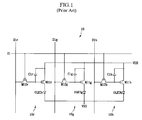
- Fig. 1 shows a pixel circuit, one of nxm pixels, which is located at a first row and a first column.
- one pixel 10 includes three sub pixels 10r, 10g, and 10b, which respectively include organic EL elements OLEDr, OLEDg, and OLEDb for respectively emitting a red light (R), a green light (G), and a blue light (B). Further, in the structure the sub pixels are arranged in a stripe format, and the sub pixels 10r, 10g, and 10b are coupled to separate data lines D1r, D1g, and D1b and to a common scan line S1.
- the red color sub pixel 10r includes two transistors M11r and M12r and a capacitor C1r for driving the organic EL element OLEDr.
- the green color sub pixel 10g includes two transistors M11g and M12g and a capacitor C1g for driving the organic EL element OLEDg
- the blue color sub pixel 10b includes two transistors M11b and M12b and a capacitor C1b for driving the organic EL element OLEDb. Since the connections and operations of the sub pixels 10r, 10g, and 10b are substantially the same, only the connection and operation of the sub pixel 10r will now be described as an example.
- the driving transistor M11r is coupled between a power supply source voltage VDD and an anode of the organic EL element OLEDr, and transmits a current for emitting light to the organic EL element OLEDr.
- a cathode of the organic EL element OLEDr is coupled to a voltage VSS which is lower than the power supply source voltage VDD.
- the amount of the current flowing in the driving transistor M11r r is controlled by a data voltage applied through the switching transistor M12r.
- the capacitor C1r is coupled between a source and a gate of the transistor M11r and controls applied voltage during a predetermined period.
- a scan line S1 for transmitting an on/off selection signal is coupled to a gate of the transistor M12r, and a data line D1r for transmitting a data voltage corresponding to the red color sub pixel 10r is coupled to a source of the transistor M 12r.
- the switching transistor M12r is turned on in response to a select signal which is applied to the gate. Then, the data voltage V DATA is applied to the gate of the transistor M11r from the data line D1r through the transistor M12r. Then, a current I OLED flows to (and/or through) the transistor M11 r corresponding to a voltage V GS which is charged between the gate and source of the transistor M11 r by the capacitor C1r.
- the organic EL element OLEDr emits red light corresponding to the current I OLED .
- the current flowing to the organic EL element OLEDr is calculated as given in the following Equation 1.
- V TH is a threshold voltage of the transistor M11r
- ⁇ is a constant.
- a current corresponding to a data voltage is supplied to an organic EL element OLEDr in the pixel circuit shown in Fig. 1 , and the organic EL element OLEDr emits a red light to brightness corresponding to the supplied current.
- the supplied data voltage has multistage voltage values in a predetermined range to display a certain gray scale.
- one pixel 10 includes three subpixels 10r, 10g, and 10b, and each sub pixel includes a driving transistor, M11r, M11g or M11b, a switching transistor, M12r, M12g or M12b, and a capacitor, C1r, C1g or C1b, for driving the organic EL element, OLEDr, OLEDg or OLEDb. Further, each sub pixel is coupled to a data line for transmitting a data signal and a power line for transmitting a power supply source voltage V DD .
- EP0762374 A discloses a driving circuit for OLED pixels in active matrix display devices.
- the subpixels of one OLED pixel share the same data line and the same current driving transistor in order to improve aperture ratio.
- the cathodes of the subpixels' LEDs are connected to the current driving transistor, the anodes are connected to a power supply line which is controlled in a time multiplexing mode to switch on the respective subpixel during a corresponding subframe.
- red, green, and blue LEDs of a pixel share the same driver circuit. Each LED is series connected to a corresponding FET for enabling current flow through the LED. The FETs are controlled by means of enable signals.
- N. Komiya et al. propose a pixel circuit for an OLED display device in "Comparison of Vth compensation ability among voltage programming circuits for AMOLED panels", IDW International Display Workshops Technical Digest, pages 275 through 278, 00-00-2003 .
- a threshold voltage compensation capacitor is connected between the gate of the driver transistor and the address transistor.
- a data voltage storage capacitor is connected between the address transistor and Vdd.
- the pixel circuit further includes a reset transistor connected to the data storage transistor and a threshold compensation transistor coupled between the gate and the drain of the driver transistor. The gates of the reset and the threshold compensation transistors are connected to a previous gate line for initialisation of the threshold compensation.
- the present invention provides a light emitting display having components that are efficiently arranged in a pixel.
- the display device comprises a plurality of scan lines for transmitting select signals, a plurality of data lines for transmitting data signals, and a plurality of pixel circuits coupled to the scan lines and the data lines.
- Each of the pixel circuits comprises first and second capacitors, first, second, third, and fourth transistors, first, second, and third emit elements, and first, second, and third emit control transistors.
- the first capacitor is provided for charging a voltage which corresponds to one of the data signals transmitted from a corresponding one of the data lines.
- the first transistor is provided for outputting a current which corresponds to the voltage charged in the first capacitor and has one of the source and the drain connected to a first power supply source.
- the second transistor is coupled between a control electrode of the first transistor and the other one of the drain and the source of the first transistor.
- the control electrode of the second transistor is coupled to a first scan line.
- the third transistor has a first one of the source and the drain coupled to a first electrode of the first capacitor and to said first power supply source, a second one of the source and the drain coupled to a second electrode of the first capacitor, and the control electrode coupled to said first scan line (Sk-1).
- the second capacitor has a first electrode coupled to the second one of the source and the drain of the third transistor and a second electrode coupled to the control electrode of the first transistor.
- the fourth transistor has a first one of the source and the drain coupled to said one of the data lines, the other one of the source and the drain coupled to the first electrode of the second capacitor, and the control electrode coupled to a second scan line.
- the first, second, and third emit elements for emitting a light corresponding to the current outputted from the first transistor each have a first electrode coupled to a second power source.
- the first, second, and third emit control transistors are respectively coupled between said other one of the drain and the source of the first transistor and the second electrode of the corresponding one of the first, second, and third emit elements.
- the control electrodes of the first, second, and third emit transistors are coupled to emit control lines.
- the first semiconductor layer forming the first emit control transistor is arranged generally symmetrically with the second semiconductor layer forming the second emit control transistor with respect to the third semiconductor layer forming the third emit control transistor.
- Fig. 1 shows a pixel circuit of a conventional light emitting display panel.
- Fig. 2 is a schematic diagram of an organic EL display according to an exemplary embodiment of the present invention.
- Fig. 3 shows an equivalent circuit of a pixel circuit according to an exemplary embodiment of the present invention.
- Fig. 4 is an arrangement diagram of a pixel circuit according to a first exemplary embodiment of the present invention.
- Fig. 5 is a cross-sectional view taken along I-I' in Fig. 4 .
- Fig. 6 is a cross-sectional view taken along II-II' in Fig. 4 .
- Fig. 7 is an arrangement diagram of a pixel circuit according to a second exemplary embodiment of the present invention.
- a present scan line refers to a scan line transmitting a present selection signal
- a previous scan line refers to a scan line that transmitted a selection signal before the present selection signal
- a present pixel refers to a pixel emitting light on the basis of a selection signal of the present scan line
- a previous pixel refers to a pixel emitting light on the basis of a selection signal of the previous scan line
- a next pixel refers to a pixel emitting light on the basis of a selection signal of the next scan line.
- the organic EL display includes a display panel 100, a scan driver 200, an emit controller 300, and a data driver 400.
- the display panel 100 includes a plurality of scan lines S0, S1, ... Sk... Sn and a plurality of emit control lines E1, ... Ek... En arranged in the row direction, a plurality of data lines D1 ... Dk... Dm and a plurality of power lines for applying power supply source voltage VDD arranged in the column direction and a plurality of pixels 110.
- Each of the pixels 110 is formed at a pixel area defined or surrounded by any two scan lines Sk-1 and Sk and any two neighboring data lines Dk-1 and Dk, and the pixels 110 are driven according to a signal transmitted from the present scan line Sk, the previous scan line Sk-1, the emit control line Ek, and the data line Dk.
- each of the emit control lines E1 to En is composed of three emit control lines (e.g., E1 includes E1r, E1g and E1b, En includes Enr, Eng and Enb, and Ek includes Ekr, Ekg and Ekb as shown in FIG. 3 ).
- the scan driver 200 sequentially applies the select signals for selecting corresponding lines to the scan lines S0 to Sn such that the data signals can be applied to the pixels of the corresponding lines.
- the emit controller 300 sequentially applies the emit control signals for controlling emission of the organic EL elements OLEDr, OLEDg, and OLEDb shown in FIG. 3 to the emit control lines E1 to En.
- the data driver 400 applies the data signals corresponding to the pixels of the lines to which the selection signals are applied, to the data lines D1 to Dm, whenever the selection signals are sequentially applied.
- the scan driver 200, the emit controller 300, and the data driver 400 can be coupled to the substrate on which the display panel 100 is formed.
- the scan driver 200, the emit controller 300, and/or the data driver 400 can be directly formed on the glass substrate of the display panel 100.
- a driving circuit composed of the scan lines, the data lines, and transistors can be formed on the substrate of the display panel 100.
- the scan driver 200, the emit controller 300, and/or the data driver 400 can be adhered and be coupled to the substrate of the display panel 100, as a tape carrier package (TCP), flexible printed circuit (FPC), or tape automatic bonding (TAB), etc.
- TCP tape carrier package
- FPC flexible printed circuit
- TAB tape automatic bonding
- one field can be divided into three subfields which are then driven. Red, green, and blue color data are applied and red, green, and blue lights are emitted at the three subfields.
- the scan driver 200 sequentially applies the select signals to the scan lines S0 to Sn at each subfield.
- the emit controller 300 sequentially applies the emit control signals to the emit control lines E1 to En such that each color organic EL element is emitted at each one subfield.
- the data driver 400 applies the data signals corresponding to red, green, and blue organic EL elements to the data lines D1 to Dm at three subfields.
- Fig. 3 shows an equivalent circuit of one pixel 110 in the organic EL display of Fig. 2 .
- a pixel Pk coupled to any k th row of scan line Sk, and k th column of data line Dk is described, and all transistors are p channel transistors.
- the pixel circuit includes a driving transistor M1, a diode transistor M3, a capacitor transistor M4, a switching transistor M5, three organic EL elements OLEDr, OLEDg, and OLEDb, and three emit control transistors M2r, M2g, and M2b for controlling the emission of three organic EL elements OLEDr, OLEDg, and OLEDb, and two capacitors Cst and Cvth.
- An emit control line Ek is composed of three emit control lines Ekr, Ekg, and Ekb.
- the emit control transistors M2r, M2g, and M2b respond to the emitting control signals transmitted through the emit control lines Ekr, Ekg, and Ekb, respectively, and selectively transmit the current transmitted from the driving transistor M1 to the organic EL elements OLEDr, OLEDg, and OLEDb.
- the transistor M5 responds to the selection signal transmitted from the scan line Sk and transmits the data voltage applied from the data line Dk to a first electrode or node B of the capacitor Cvth.
- the transistor M4 responds to the selection signal transmitted from the previous scan line Sk-1 and couples the node B of the capacitor Cvth to the power supply source VDD.
- the transistor M3 is coupled between a second electrode or a node A of the capacitor Cvth and a drain of the transistor M1. The transistor M3 is turned on in response to the selection signal transmitted from the previous scan line Sk-1 such that the transistor M1 is diode-connected.
- the driving transistor M1 for driving the organic EL element OLED (e.g., OLEDr, OLEDg and/or OLEDb), has its gate coupled to the node A of the capacitor Cvth, and its source coupled to the power supply source VDD.
- the driving transistor M1 controls the current that is applied to the organic EL element OLED according to the voltage that is applied to the gate.
- a first electrode of the capacitor Cst is coupled to the power supply source VDD, and a second electrode of the capacitor Cst is coupled to the drain of the transistor M4 at or about the node B, and the first electrode of the capacitor Cvth is coupled to the second electrode of the capacitor Cst such that the two capacitors are coupled in series, and the second electrode of the capacitor Cvth is coupled to the gate of the driving transistor M1 at or about the node A.
- the drain of the driving transistor M1 is coupled to the sources of the emit control transistors M2r, M2g, and M2b, and gates of the transistors M2r, M2g, and M2b are respectively coupled to the emit control lines Ekr, Ekg and Ekb. Drains of the emit control transistors M2r, M2g, and M2b are respectively coupled to anodes of organic EL elements OLEDr, OLEDg, and OLEDb.
- a power supply source V SS having a voltage level lower than that of the power supply source V DD is applied to the cathodes of the organic EL elements OLEDr, OLEDg, and OLEDb.
- a negative voltage or ground voltage can be used for the power supply source Vss.
- the transistors M3 and M4 are turned on.
- the transistor M1 comes to be in a diode-connected state.
- the voltage difference between the gate and source of the transistor M1 is changed until the voltage difference becomes a threshold voltage Vth of the transistor M1.
- a sum of the power supply source voltage V DD and the threshold voltage Vth is applied to the gate of the transistor M1, that is, at or about the node A of the capacitor Cvth.
- Cvth refers to a voltage that is charged at the capacitor Cvth
- V CvthA refers to a voltage that is applied to the node A of the capacitor Cvth
- V CvthB refers to a voltage that is applied to the node B of the capacitor Cvth.
- the transistor M5 When the low level scan voltage is applied to the present scan line Sk, the transistor M5 is turned on, and the data voltage Vdata is applied to the node B. Further, since the voltage corresponding to the threshold voltage Vth of the transistor M1 is charged at the capacitor Cvth, a voltage corresponding to the sum of the data voltage Vdata and the threshold voltage Vth is applied to the gate of the transistor M1. That is, the voltage Vgs between the gate and source of the transistor M1 can be calculated as given in the following Equation 3.
- a high-level signal is applied to the emit control line Ek (e.g., Ekr, Ekg and/or Ekb), and the transistor M2 (e.g., M2r, M2g and/or M2b) is turned off to block a current flow.
- Ek e.g., Ekr, Ekg and/or Ekb
- M2 e.g., M2r, M2g and/or M2b
- the transistor M2 is turned on in response to a low-level signal from the emit control line Ek.
- the current I OLED corresponding to the gate-source voltage Vgs of the transistor M1 is supplied to the organic EL element through the transistor M2, and the organic EL element OLED (e.g., OLEDr, OLEDg, and/or OLEDb) is emitted.
- I OLED indicates a current flowing into the organic EL element OLED
- V GS indicates a voltage between the source and the gate of the transistor M1
- Vth indicates a threshold voltage of the transistor M1
- Vdata indicates a data voltage
- ⁇ indicates a constant.
- the emit control transistor M2r When the data voltage Vdata is a red data signal, and the emit control transistor M2r is turned on in response to the low-level emit control signal transmitted from the emit control line Ekr, the current I OLED is transmitted to the red organic EL element OLEDr and the emission of red light occurs.
- an arrangement structure in a pixel area where a pixel circuit is arranged is described in detail with reference to Fig. 4 , Fig. 5 , and Fig. 6 .
- reference numerals are provided to the components of the present pixel Pk, and the same reference numerals are provided to the components of the previous pixel Pk-1, except that an apostrophe symbol (" ' ”) is added to the reference numerals.
- the apostrophe symbol (" ' ") is used to distinguish the components of the present pixel from the components of the previous pixel.
- Fig. 4 is an arrangement diagram of a pixel area in which the pixel circuit shown in Fig. 3 is arranged, according to the first exemplary embodiment of the present invention.
- Fig. 5 is a cross-sectional view taken along I-I' in Fig. 4 .
- Fig. 6 is a cross-sectional view taken along II-II' in Fig. 4 .
- a cut off layer 3 is formed on an insulated substrate 1.
- the cut off layer 3 is composed of material such as silicon oxide, or the like.
- Polysilicon layers 21, 22, 23, 24, 25, 26, 27, 28, and 29 that are semiconductor layers are formed on the cut off layer 3.
- the polysilicon layer 21 forms a semiconductor layer including a source area, a drain area, and a channel area of the transistor M5 in the present pixel Pk, of which shape resembles the letter 'U'.
- the polysilicon layer 22 forms a semiconductor layer including a source area, a drain area and a channel area of the transistor M2r in the present pixel Pk, of which shape resembles the shape.
- the polysilicon layer 23 forms a semiconductor layer including a source area, a drain area, and a channel area of the transistor M2g in the present pixel Pk, which is arranged in the column direction.
- the polysilicon layer 24 forms a semiconductor layer including the source area, the drain area and the channel area of the transistor M2b in the present pixel Pk, of which shape resembles the shape
- the polysilicon layers 22, 23, and 24 are coupled to form a shape of the letter 'm'.
- the polysilicon layer 22 is located at the left side of the polysilicon layer 23, and the polysilicon layer 24 is located at the right side of the polysilicon layer 23.
- the polysilicon layer 22 is generally symmetrical with the polysilicon layer 24 with respect to the polysilicon layer 23.
- the polysilicon layer 25 is located at or about the middle of the pixel area and is arranged in the column direction, and the bottom end of the polysilicon layer 25 is coupled to the polysilicon layers 22, 23, and 24.
- the polysilicon layer 26 is located at the left side of the polysilicon layer 25, and the polysilicon layer 27 is located at the right side of the polysilicon layer 25.
- the polysilicon layer 26 is generally symmetrical with the polysilicon layer 27 with respect to the polysilicon layer 25.
- the polysilicon layer 26 generally has a shape of a square and forms a second electrode (node A) of the capacitor Cvth, and the polysilicon layer 27, which generally has a shape of a rectangle, forms a first electrode of the capacitor Cst.
- the polysilicon layer 28 has a shape of the letter 'n', and one end of the polysilicon layer 28 is coupled to the polysilicon layer 26 and other end of the polysilicon layer 28 is coupled to the polysilicon layer 25 and forms the source, drain, and channel area of the transistor M3.
- the polysilicon layer 29 has a shape of the letter 'n', and one end of the polysilicon layer 29 is coupled to the polysilicon layer 28 and forms the channel area and drain area of the transistor M1, and the source area, channel area, and drain area of the transistor M4.
- a gate insulating film 30 is formed on the polysilicon layers 21 to 29.
- the gates 41, 42, 43, 44, 45, 46, and 47 are formed on the gate insulating film 30.
- the gate line 41 is arranged in the row direction, and corresponds to the present scan line Sk of the present pixel Pk, and the gate line 41 is insulated and crosses the polysilicon layer 21 to form the gate of the transistor M5 in the present pixel Pk.
- the gate line 42 is arranged in the row direction, and corresponds to the emit control line Ekb in the present pixel Pk, to form the gate of the transistor M2b.
- the gate line 43 is arranged in the row direction, and corresponds to the emit control line Ekg of the present pixel Pk, to form the gate of the transistor M2g.
- the gate line 44 is arranged in the row direction, and corresponds to the emit control line Ekr of the present pixel Pk, to form the gate of the transistor M2r.
- the gate line 45 is insulated and crosses the polysilicon layer 26 to form the gate of the transistor M1.
- the gate 46 which generally has a shape of a square, is arranged on the polysilicon layer 26 to form the first electrode (node B) of the capacitor Cvth.
- the gate 47 which generally has a shape of a rectangle, is arranged on the polysilicon layer 27 to form the second electrode (node B) of the capacitor Cst.
- the gate line 41' is arranged in the row direction; it corresponds to the previous scan line Sk-1 of the previous pixel Pk-1, and is insulated and crosses the polysilicon layer 21' to form the gate of the transistor M5 of the previous pixel Pk-1. Further, the gate line 41' is insulated and crosses the polysilicon layers 28 and 29 to form gates of the transistors M3 and M4 of the present pixel Pk.
- the layer insulating film 50 is formed on the gates 41, 42, 43, 44, 45, 46, and 47.
- a data line 61, a power line 62, and electrodes 63, 64, 65, 66r, 66g, and 66b are formed on the layer insulating film 50, such that the data line 61, the power line 62, and the electrodes 63, 64, 65, 66r, 66g, and 66b are contacted to the corresponding electrodes through contact holes 51a, 51b, 53, 54a, 54b, 55, 56a, 56b, 57r, 57g, and 57b.
- the data line 61 is arranged in the column direction between two pixel areas and is coupled to the polysilicon layer 21 through the contact hole 51a such that the data line 61 is coupled to the source of the transistor M5.
- the contact hole 51a passes through the layer insulating film 50 and the gate insulating film 30.
- the power supply source line 62 is arranged in the column direction and is coupled to the polysilicon layers 27 and 29 through the contact hole 55 such that the power supply source line 62 supplies power to the first electrode of the capacitor Cst and the source of the transistor M1.
- the contact hole 55 passes through the layer insulating film 50 and the gate insulating film 30.
- the electrode 63 is close to the data line 61, is substantially parallel with the data line 61, and couples the drain area of the polysilicon layer 21 to the gate 46 through the contact hole 51 b penetrating the layer insulating film 50 and the gate insulating film 30, and the contact hole 53 penetrating the layer insulating film 50.
- the electrode 63 becomes the node B.
- the electrode 64 is close to the gate 41', is substantially parallel with the gate 41', and couples the drain area to the gate 45 of the transistor M3 in the polysilicon layer 28 through the contact hole 54a penetrating the layer insulating film 50 and the gate insulating film 30, and the contact hole 54b penetrating the layer insulating film 50.
- the electrode 64 becomes the node A.
- the electrode 65 which substantially has a shape of a rectangle, is close to the gate 41' and couples the drain area to the gate 47 of the transistor M4 in the polysilicon layer 29 through the contact hole 56a penetrating the layer insulating film 50 and the gate insulating film 30, and the contact hole 56b penetrating the layer insulating film 50.
- the electrode 65 becomes the node B.
- the electrodes 66r, 66g, and 66b respectively couple the pixel electrodes 81r, 81g, and 81b of each emit element to the drains of the transistors M2r, M2g, and M2b.
- their row directions are longer than their column directions.
- the data line 62 is arranged in the column line, and the gates 42 to 44 are arranged in the row direction.
- the electrodes 66r, 66g, and 66b are respectively coupled to the polysilicon layers 22, 23, and 24 through the contact holes 57r, 57g, and 57b penetrating the gate insulating film 30 and the layer insulating film 50, and are coupled to the drains of the transistors M2r, M2g, and M2b.
- a flatting film 70 is formed on the electrodes 63, 64, 65, 66r, 66g, and 66b.
- the pixel electrodes 81r, 81g, and 81b are respectively coupled to the electrodes 66r, 66g, and 66b through the contact holes 71r, 71g, and 71b.
- the poly layer structure of red, green, and blue organic films 85r, 85g, and 85b including an emitting layer (EML), an electron transporting layer (ETL), and a hole transporting layer (HTL) are formed on the pixel electrodes 81r, 81g, and 81b.
- the polysilicon layers 22, 23, and 24 forming the emit control transistor are coupled to each other.
- the polysilicon layer 23 forms the emit control transistor M2g of the organic EL element located in the middle of the three organic EL elements.
- the polysilicon layer 22 forms the emit control transistor M2r of the organic EL element located in the left side of the three organic EL elements.
- the polysilicon layer 24 forms the emit control transistor M2b of the organic EL element located in the right side of the three organic EL elements.
- the polysilicon layer 22 is arranged generally symmetrically with the polysilicon layer 24 with respect to the polysilicon layer 23.
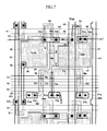
- the second exemplary embodiment of the present invention is different from the first exemplary embodiment in that each of polysilicon layers 122, 123, and 124 for respectively forming emit control transistors M2r, M2g, and M2b, has a substantially constant ratio of length and width such that the emit control transistors M2r, M2g, and M2b have similar or substantially the same inner resistances.
- each of polysilicon layers 122, 123, and 124 for respectively forming emit control transistors M2r, M2g, and M2b has a substantially constant ratio of length and width such that the emit control transistors M2r, M2g, and M2b have similar or substantially the same inner resistances.
- the polysilicon layer 122 has length Lr and width Wr
- the polysilicon layer 123 has length Lg and width Wg
- the polysilicon layer 124 has length Lb and width Wb.
- the inner resistance of the polysilicon layer can be calculated as given in the following Equation 5.
- R R S ⁇ L W
- the R is the inner resistance of the polysilicon layer
- L is the length of the polysilicon layer, that is, the sum of the lengths of the source area, the channel area, and the drain area
- W is the width of the polysilicon layer in a direction that is substantially perpendicular to the direction in which the length is measured.
- Rs is a plane resistance, which is a resistance of the polysilicon layer having the unit width W and unit length L.
- the plane resistance may have a value of 5 ⁇ /plane.
- each inner resistance of each polysilicon layer 122, 123, and 124 depends on each of Lr/Wr, Lg/Wg, and Lb/Wb.
- the polysilicon layers 122, 123, and 124 have correlation such as given in the following Equation 6, such that the inner resistances R of each polysilicon layer 122, 123, and 124 have similar or substantially the same values.
- the properties of the emit control transistors M2r, M2g, and M2b can be substantially constantly maintained by using the polysilicon layers 122, 123, and 124 having substantially the same ratio of (or between) the length and the width.
- the properties of the emit control transistors M2r, M2g and M2b can be established to be substantially the same as each other by using the polysilicon layers 122, 123, and 124 having substantially the same ratio of length and width, such that the current I OLED transmitted through the emit control transistors M2r, M2g, and M2b can be substantially constantly maintained.
- polysilicon layers forming the emit control transistors are coupled to be one body. Further, when the polysilicon layer forming the emit control transistor of the organic EL element which is located in the middle of the three organic EL elements, is located in the middle, the polysilicon layer which is located at the left side of the three organic EL elements is arranged generally symmetrically with the polysilicon layer which is located at the right side of the three organic EL elements with respect to the polysilicon layer which is located in the middle. Further, the emit control transistors can have substantially the same properties by using the polysilicon layers having substantially the same ratio of length and width.
- each element is more efficiently arranged at the small pixel area, while the inner resistances of the polysilicon layers forming the emit control transistors are substantially constantly maintained. Further, the emit control transistors have substantially the same current transmitting properties, and thus the current outputted from the driving transistor can be substantially stably transmitted to the corresponding emit elements.
Landscapes
- Engineering & Computer Science (AREA)
- Physics & Mathematics (AREA)
- Computer Hardware Design (AREA)
- General Physics & Mathematics (AREA)
- Theoretical Computer Science (AREA)
- Geometry (AREA)
- Microelectronics & Electronic Packaging (AREA)
- Electroluminescent Light Sources (AREA)
- Control Of El Displays (AREA)
- Control Of Indicators Other Than Cathode Ray Tubes (AREA)
- Devices For Indicating Variable Information By Combining Individual Elements (AREA)
- Thin Film Transistor (AREA)
Abstract
Description
- The present invention relates to a display device. More particularly, the present invention relates to an organic electroluminescent display using electroluminescence (hereinafter, 'EL') of organic materials.
- In general, an organic electroluminescent (EL) display electrically excites a phosphorous organic compound to emit light. The organic emitting elements (or organic emitting cells) are arranged in an nxm matrix format to configure an organic EL display panel which displays image data by voltage- or current-driving.
- The organic emit element has diode properties, and thus is also referred to as an organic light emitting diode (OLED). The organic emit element includes an anode (ITO), an organic thin film, and a cathode layer (metal). The organic thin film has a multi-layer structure including an emitting layer (EML), an electron transport layer (ETL), and a hole transport layer (HTL) for maintaining balance between electrons and holes and improving emitting efficiencies. Further, the organic emitting element includes an electron injecting layer (EIL) and a hole injecting layer (HIL). The organic emitting elements are arranged in an nxm matrix format to configure an organic EL display panel.
- Methods for driving the organic EL display panel include a passive matrix method, and an active matrix method which uses thin-film transistors (TFTs). The passive matrix method includes forming anodes and cathodes to cross (or cross over) with or to be substantially perpendicular to each other, selecting lines, and driving the organic EL display panel. The active matrix method includes orderly turning on of a plurality of TFTs which are respectively coupled to data lines and scan lines according to signals for selecting the scan lines and driving the organic EL display panel.
- Hereinafter, a pixel circuit of a general active matrix organic EL display is described.
-
Fig. 1 shows a pixel circuit, one of nxm pixels, which is located at a first row and a first column. - As shown in
Fig. 1 , onepixel 10 includes threesub pixels sub pixels - The red
color sub pixel 10r includes two transistors M11r and M12r and a capacitor C1r for driving the organic EL element OLEDr. In the same manner, the greencolor sub pixel 10g includes two transistors M11g and M12g and a capacitor C1g for driving the organic EL element OLEDg, and the bluecolor sub pixel 10b includes two transistors M11b and M12b and a capacitor C1b for driving the organic EL element OLEDb. Since the connections and operations of thesub pixels sub pixel 10r will now be described as an example. - The driving transistor M11r is coupled between a power supply source voltage VDD and an anode of the organic EL element OLEDr, and transmits a current for emitting light to the organic EL element OLEDr. A cathode of the organic EL element OLEDr is coupled to a voltage VSS which is lower than the power supply source voltage VDD. The amount of the current flowing in the driving transistor M11r r is controlled by a data voltage applied through the switching transistor M12r. The capacitor C1r is coupled between a source and a gate of the transistor M11r and controls applied voltage during a predetermined period. A scan line S1 for transmitting an on/off selection signal is coupled to a gate of the transistor M12r, and a data line D1r for transmitting a data voltage corresponding to the red
color sub pixel 10r is coupled to a source of the transistor M 12r. - Here, the switching transistor M12r is turned on in response to a select signal which is applied to the gate. Then, the data voltage VDATA is applied to the gate of the transistor M11r from the data line D1r through the transistor M12r. Then, a current IOLED flows to (and/or through) the transistor M11 r corresponding to a voltage VGS which is charged between the gate and source of the transistor M11 r by the capacitor C1r. The organic EL element OLEDr emits red light corresponding to the current IOLED. The current flowing to the organic EL element OLEDr is calculated as given in the following
Equation 1.
- Here, VTH is a threshold voltage of the transistor M11r, and β is a constant.
- As represented by
Equation 1, a current corresponding to a data voltage is supplied to an organic EL element OLEDr in the pixel circuit shown inFig. 1 , and the organic EL element OLEDr emits a red light to brightness corresponding to the supplied current. Here, the supplied data voltage has multistage voltage values in a predetermined range to display a certain gray scale. - As such, in the organic EL display, one
pixel 10 includes threesubpixels - Therefore, many lines for transmitting voltages and signals to a transistor and a capacitor are required to be located in each pixel, and there is difficulty to arrange all the lines within one pixel.
-
EP0762374 A discloses a driving circuit for OLED pixels in active matrix display devices. The subpixels of one OLED pixel share the same data line and the same current driving transistor in order to improve aperture ratio. The cathodes of the subpixels' LEDs are connected to the current driving transistor, the anodes are connected to a power supply line which is controlled in a time multiplexing mode to switch on the respective subpixel during a corresponding subframe. - In
US6618031 B1 red, green, and blue LEDs of a pixel share the same driver circuit. Each LED is series connected to a corresponding FET for enabling current flow through the LED. The FETs are controlled by means of enable signals. - N. Komiya et al. propose a pixel circuit for an OLED display device in "Comparison of Vth compensation ability among voltage programming circuits for AMOLED panels", IDW International Display Workshops Technical Digest, pages 275 through 278, 00-00-2003. There, a threshold voltage compensation capacitor is connected between the gate of the driver transistor and the address transistor. A data voltage storage capacitor is connected between the address transistor and Vdd. The pixel circuit further includes a reset transistor connected to the data storage transistor and a threshold compensation transistor coupled between the gate and the drain of the driver transistor. The gates of the reset and the threshold compensation transistors are connected to a previous gate line for initialisation of the threshold compensation.
- The present invention provides a light emitting display having components that are efficiently arranged in a pixel. The display device comprises a plurality of scan lines for transmitting select signals, a plurality of data lines for transmitting data signals, and a plurality of pixel circuits coupled to the scan lines and the data lines. Each of the pixel circuits comprises first and second capacitors, first, second, third, and fourth transistors, first, second, and third emit elements, and first, second, and third emit control transistors. The first capacitor is provided for charging a voltage which corresponds to one of the data signals transmitted from a corresponding one of the data lines. The first transistor is provided for outputting a current which corresponds to the voltage charged in the first capacitor and has one of the source and the drain connected to a first power supply source. The second transistor is coupled between a control electrode of the first transistor and the other one of the drain and the source of the first transistor. The control electrode of the second transistor is coupled to a first scan line. The third transistor has a first one of the source and the drain coupled to a first electrode of the first capacitor and to said first power supply source, a second one of the source and the drain coupled to a second electrode of the first capacitor, and the control electrode coupled to said first scan line (Sk-1). The second capacitor has a first electrode coupled to the second one of the source and the drain of the third transistor and a second electrode coupled to the control electrode of the first transistor. The fourth transistor has a first one of the source and the drain coupled to said one of the data lines, the other one of the source and the drain coupled to the first electrode of the second capacitor, and the control electrode coupled to a second scan line. The first, second, and third emit elements for emitting a light corresponding to the current outputted from the first transistor each have a first electrode coupled to a second power source. The first, second, and third emit control transistors are respectively coupled between said other one of the drain and the source of the first transistor and the second electrode of the corresponding one of the first, second, and third emit elements. The control electrodes of the first, second, and third emit transistors are coupled to emit control lines. According to the invention, the first semiconductor layer forming the first emit control transistor is arranged generally symmetrically with the second semiconductor layer forming the second emit control transistor with respect to the third semiconductor layer forming the third emit control transistor.
- The accompanying drawings, together with the specification, illustrate exemplary embodiments of the present invention, and, together with the description, serve to explain the principles of the present invention.
-
Fig. 1 shows a pixel circuit of a conventional light emitting display panel. -
Fig. 2 is a schematic diagram of an organic EL display according to an exemplary embodiment of the present invention. -
Fig. 3 shows an equivalent circuit of a pixel circuit according to an exemplary embodiment of the present invention. -
Fig. 4 is an arrangement diagram of a pixel circuit according to a first exemplary embodiment of the present invention. -
Fig. 5 is a cross-sectional view taken along I-I' inFig. 4 . -
Fig. 6 is a cross-sectional view taken along II-II' inFig. 4 . -
Fig. 7 is an arrangement diagram of a pixel circuit according to a second exemplary embodiment of the present invention. - In the following detailed description, only certain exemplary embodiments of the present invention are shown and described, simply by way of illustration. As those skilled in the art would recognize, the described exemplary embodiments may be modified in various ways, all without departing from the spirit or scope of the present invention. Accordingly, the drawings and description are to be regarded as illustrative in nature, and not restrictive.
- There may be parts shown in the drawings, or parts not shown in the drawings, that are not discussed in the specification as they are not essential to a complete understanding of the invention. Like reference numerals designate like elements. The thickness is magnified to more clearly show several layers and areas in the drawings. When a layer, a membrane, a board, etc., is described to be located 'on' another part, it is understood that a further part can be located therebetween.
- In addition, several terms for scan lines are defined. "A present scan line" refers to a scan line transmitting a present selection signal, and "a previous scan line" refers to a scan line that transmitted a selection signal before the present selection signal.
- Further, "a present pixel" refers to a pixel emitting light on the basis of a selection signal of the present scan line, "a previous pixel" refers to a pixel emitting light on the basis of a selection signal of the previous scan line, and "a next pixel" refers to a pixel emitting light on the basis of a selection signal of the next scan line.
- As shown in
Fig. 2 , the organic EL display according to an exemplary embodiment of the present invention includes adisplay panel 100, ascan driver 200, an emitcontroller 300, and adata driver 400. Thedisplay panel 100 includes a plurality of scan lines S0, S1, ... Sk... Sn and a plurality of emit control lines E1, ... Ek... En arranged in the row direction, a plurality of data lines D1 ... Dk... Dm and a plurality of power lines for applying power supply source voltage VDD arranged in the column direction and a plurality ofpixels 110. Each of thepixels 110 is formed at a pixel area defined or surrounded by any two scan lines Sk-1 and Sk and any two neighboring data lines Dk-1 and Dk, and thepixels 110 are driven according to a signal transmitted from the present scan line Sk, the previous scan line Sk-1, the emit control line Ek, and the data line Dk. Further, each of the emit control lines E1 to En is composed of three emit control lines (e.g., E1 includes E1r, E1g and E1b, En includes Enr, Eng and Enb, and Ek includes Ekr, Ekg and Ekb as shown inFIG. 3 ). - The
scan driver 200 sequentially applies the select signals for selecting corresponding lines to the scan lines S0 to Sn such that the data signals can be applied to the pixels of the corresponding lines. The emitcontroller 300 sequentially applies the emit control signals for controlling emission of the organic EL elements OLEDr, OLEDg, and OLEDb shown inFIG. 3 to the emit control lines E1 to En. Thedata driver 400 applies the data signals corresponding to the pixels of the lines to which the selection signals are applied, to the data lines D1 to Dm, whenever the selection signals are sequentially applied. - The
scan driver 200, the emitcontroller 300, and thedata driver 400 can be coupled to the substrate on which thedisplay panel 100 is formed. Alternatively, thescan driver 200, the emitcontroller 300, and/or thedata driver 400 can be directly formed on the glass substrate of thedisplay panel 100. Further, a driving circuit composed of the scan lines, the data lines, and transistors can be formed on the substrate of thedisplay panel 100. Further, thescan driver 200, the emitcontroller 300, and/or thedata driver 400 can be adhered and be coupled to the substrate of thedisplay panel 100, as a tape carrier package (TCP), flexible printed circuit (FPC), or tape automatic bonding (TAB), etc. - In exemplary embodiments of the present invention, one field can be divided into three subfields which are then driven. Red, green, and blue color data are applied and red, green, and blue lights are emitted at the three subfields. Here, the
scan driver 200 sequentially applies the select signals to the scan lines S0 to Sn at each subfield. The emitcontroller 300 sequentially applies the emit control signals to the emit control lines E1 to En such that each color organic EL element is emitted at each one subfield. Thedata driver 400 applies the data signals corresponding to red, green, and blue organic EL elements to the data lines D1 to Dm at three subfields. - Hereinafter, the detailed operation of the organic EL display according to an exemplary embodiment of the present invention will be described in detail with reference to
Fig. 3 . -
Fig. 3 shows an equivalent circuit of onepixel 110 in the organic EL display ofFig. 2 . InFig. 3 , for example, a pixel Pk coupled to any kth row of scan line Sk, and kth column of data line Dk is described, and all transistors are p channel transistors. - As shown in
Fig. 3 , the pixel circuit according to the exemplary embodiment of the present invention includes a driving transistor M1, a diode transistor M3, a capacitor transistor M4, a switching transistor M5, three organic EL elements OLEDr, OLEDg, and OLEDb, and three emit control transistors M2r, M2g, and M2b for controlling the emission of three organic EL elements OLEDr, OLEDg, and OLEDb, and two capacitors Cst and Cvth. An emit control line Ek is composed of three emit control lines Ekr, Ekg, and Ekb. The emit control transistors M2r, M2g, and M2b respond to the emitting control signals transmitted through the emit control lines Ekr, Ekg, and Ekb, respectively, and selectively transmit the current transmitted from the driving transistor M1 to the organic EL elements OLEDr, OLEDg, and OLEDb. - In detail, the transistor M5, of which the gate is coupled to the present scan line Sk and the source is coupled to the data line Dk, responds to the selection signal transmitted from the scan line Sk and transmits the data voltage applied from the data line Dk to a first electrode or node B of the capacitor Cvth. The transistor M4 responds to the selection signal transmitted from the previous scan line Sk-1 and couples the node B of the capacitor Cvth to the power supply source VDD. The transistor M3 is coupled between a second electrode or a node A of the capacitor Cvth and a drain of the transistor M1. The transistor M3 is turned on in response to the selection signal transmitted from the previous scan line Sk-1 such that the transistor M1 is diode-connected. The driving transistor M1, for driving the organic EL element OLED (e.g., OLEDr, OLEDg and/or OLEDb), has its gate coupled to the node A of the capacitor Cvth, and its source coupled to the power supply source VDD. The driving transistor M1 controls the current that is applied to the organic EL element OLED according to the voltage that is applied to the gate.
- Further, a first electrode of the capacitor Cst is coupled to the power supply source VDD, and a second electrode of the capacitor Cst is coupled to the drain of the transistor M4 at or about the node B, and the first electrode of the capacitor Cvth is coupled to the second electrode of the capacitor Cst such that the two capacitors are coupled in series, and the second electrode of the capacitor Cvth is coupled to the gate of the driving transistor M1 at or about the node A.
- The drain of the driving transistor M1 is coupled to the sources of the emit control transistors M2r, M2g, and M2b, and gates of the transistors M2r, M2g, and M2b are respectively coupled to the emit control lines Ekr, Ekg and Ekb. Drains of the emit control transistors M2r, M2g, and M2b are respectively coupled to anodes of organic EL elements OLEDr, OLEDg, and OLEDb. A power supply source VSS having a voltage level lower than that of the power supply source VDD is applied to the cathodes of the organic EL elements OLEDr, OLEDg, and OLEDb. A negative voltage or ground voltage can be used for the power supply source Vss.
- When a low level scan voltage is applied to the previous scan line Sk-1, the transistors M3 and M4 are turned on. When the transistor M3 is turned on, the transistor M1 comes to be in a diode-connected state. Thus, the voltage difference between the gate and source of the transistor M1 is changed until the voltage difference becomes a threshold voltage Vth of the transistor M1. At this time, since the source of the transistor M1 is coupled to the power supply source VDD, a sum of the power supply source voltage VDD and the threshold voltage Vth is applied to the gate of the transistor M1, that is, at or about the node A of the capacitor Cvth. Further, when the transistor M4 is turned on and the power supply source voltage VDD is applied to the node B, the voltage Vcvth charged at the capacitor Cvth can be calculated as given in the following Equation 2.

- Here, Cvth refers to a voltage that is charged at the capacitor Cvth, VCvthA refers to a voltage that is applied to the node A of the capacitor Cvth, and VCvthB refers to a voltage that is applied to the node B of the capacitor Cvth.
- When the low level scan voltage is applied to the present scan line Sk, the transistor M5 is turned on, and the data voltage Vdata is applied to the node B. Further, since the voltage corresponding to the threshold voltage Vth of the transistor M1 is charged at the capacitor Cvth, a voltage corresponding to the sum of the data voltage Vdata and the threshold voltage Vth is applied to the gate of the transistor M1. That is, the voltage Vgs between the gate and source of the transistor M1 can be calculated as given in the following
Equation 3. Here, a high-level signal is applied to the emit control line Ek (e.g., Ekr, Ekg and/or Ekb), and the transistor M2 (e.g., M2r, M2g and/or M2b) is turned off to block a current flow.
- Next, the transistor M2 is turned on in response to a low-level signal from the emit control line Ek. Thus, the current IOLED corresponding to the gate-source voltage Vgs of the transistor M1 is supplied to the organic EL element through the transistor M2, and the organic EL element OLED (e.g., OLEDr, OLEDg, and/or OLEDb) is emitted. The current IOLED can be calculated as in the following Equation 4.

- Here, IOLED indicates a current flowing into the organic EL element OLED, VGS indicates a voltage between the source and the gate of the transistor M1, Vth indicates a threshold voltage of the transistor M1, Vdata indicates a data voltage, and β indicates a constant.
- When the data voltage Vdata is a red data signal, and the emit control transistor M2r is turned on in response to the low-level emit control signal transmitted from the emit control line Ekr, the current IOLED is transmitted to the red organic EL element OLEDr and the emission of red light occurs.
- In the same manner, when the data voltage Vdata is a green data signal, and the emit control transistor M2g is turned on in response to the low-level emit control signal transmitted from the emit control line Ekg, the current IOLED is transmitted to the green organic EL element OLEDg and the emission of green light occurs. Further, when the data voltage Vdata is a blue data signal, and the emit control transistor M2b is turned on in response to the low-level emit control signal transmitted from the emit control line Ekb, the current IOLED is transmitted to the blue organic EL element OLEDb and the emission of blue light occurs. Three emit control signals that are applied to three emit control lines respectively have low level periods that are not overlapped with each other during one field, such that one pixel can display red, green, and blue colors.
- Next, in an organic EL display according to a first exemplary embodiment of the present invention, an arrangement structure in a pixel area where a pixel circuit is arranged is described in detail with reference to
Fig. 4 ,Fig. 5 , andFig. 6 . Here, reference numerals are provided to the components of the present pixel Pk, and the same reference numerals are provided to the components of the previous pixel Pk-1, except that an apostrophe symbol (" ' ") is added to the reference numerals. The apostrophe symbol (" ' ") is used to distinguish the components of the present pixel from the components of the previous pixel. -
Fig. 4 is an arrangement diagram of a pixel area in which the pixel circuit shown inFig. 3 is arranged, according to the first exemplary embodiment of the present invention.Fig. 5 is a cross-sectional view taken along I-I' inFig. 4 .Fig. 6 is a cross-sectional view taken along II-II' inFig. 4 . - First, as shown in
Fig. 4 ,Fig. 5 , andFig. 6 , a cut offlayer 3 is formed on aninsulated substrate 1. The cut offlayer 3 is composed of material such as silicon oxide, or the like. Polysilicon layers 21, 22, 23, 24, 25, 26, 27, 28, and 29 that are semiconductor layers are formed on the cut offlayer 3. - The
polysilicon layer 21 forms a semiconductor layer including a source area, a drain area, and a channel area of the transistor M5 in the present pixel Pk, of which shape resembles the letter 'U'. Thepolysilicon layer 22 forms a semiconductor layer including a source area, a drain area and a channel area of the transistor M2r in the present pixel Pk, of which shape resembles the shapeThe
polysilicon layer 23 forms a semiconductor layer including a source area, a drain area, and a channel area of the transistor M2g in the present pixel Pk, which is arranged in the column direction. Thepolysilicon layer 24 forms a semiconductor layer including the source area, the drain area and the channel area of the transistor M2b in the present pixel Pk, of which shape resembles the shapeThe polysilicon layers 22, 23, and 24 are coupled to form a shape of the letter 'm'. Thepolysilicon layer 22 is located at the left side of thepolysilicon layer 23, and thepolysilicon layer 24 is located at the right side of thepolysilicon layer 23. Thepolysilicon layer 22 is generally symmetrical with thepolysilicon layer 24 with respect to thepolysilicon layer 23. - The
polysilicon layer 25 is located at or about the middle of the pixel area and is arranged in the column direction, and the bottom end of thepolysilicon layer 25 is coupled to the polysilicon layers 22, 23, and 24. Thepolysilicon layer 26 is located at the left side of thepolysilicon layer 25, and thepolysilicon layer 27 is located at the right side of thepolysilicon layer 25. Thepolysilicon layer 26 is generally symmetrical with thepolysilicon layer 27 with respect to thepolysilicon layer 25. Thepolysilicon layer 26 generally has a shape of a square and forms a second electrode (node A) of the capacitor Cvth, and thepolysilicon layer 27, which generally has a shape of a rectangle, forms a first electrode of the capacitor Cst. Thepolysilicon layer 28 has a shape of the letter 'n', and one end of thepolysilicon layer 28 is coupled to thepolysilicon layer 26 and other end of thepolysilicon layer 28 is coupled to thepolysilicon layer 25 and forms the source, drain, and channel area of the transistor M3. Thepolysilicon layer 29 has a shape of the letter 'n', and one end of thepolysilicon layer 29 is coupled to thepolysilicon layer 28 and forms the channel area and drain area of the transistor M1, and the source area, channel area, and drain area of the transistor M4. - A
gate insulating film 30 is formed on the polysilicon layers 21 to 29. - The
gates gate insulating film 30. In detail, thegate line 41 is arranged in the row direction, and corresponds to the present scan line Sk of the present pixel Pk, and thegate line 41 is insulated and crosses thepolysilicon layer 21 to form the gate of the transistor M5 in the present pixel Pk. Thegate line 42 is arranged in the row direction, and corresponds to the emit control line Ekb in the present pixel Pk, to form the gate of the transistor M2b. Thegate line 43 is arranged in the row direction, and corresponds to the emit control line Ekg of the present pixel Pk, to form the gate of the transistor M2g. Thegate line 44 is arranged in the row direction, and corresponds to the emit control line Ekr of the present pixel Pk, to form the gate of the transistor M2r. Thegate line 45 is insulated and crosses thepolysilicon layer 26 to form the gate of the transistor M1. Thegate 46, which generally has a shape of a square, is arranged on thepolysilicon layer 26 to form the first electrode (node B) of the capacitor Cvth. Thegate 47, which generally has a shape of a rectangle, is arranged on thepolysilicon layer 27 to form the second electrode (node B) of the capacitor Cst. - The gate line 41' is arranged in the row direction; it corresponds to the previous scan line Sk-1 of the previous pixel Pk-1, and is insulated and crosses the polysilicon layer 21' to form the gate of the transistor M5 of the previous pixel Pk-1. Further, the gate line 41' is insulated and crosses the polysilicon layers 28 and 29 to form gates of the transistors M3 and M4 of the present pixel Pk.
- The
layer insulating film 50 is formed on thegates data line 61, apower line 62, andelectrodes layer insulating film 50, such that thedata line 61, thepower line 62, and theelectrodes contact holes - The
data line 61 is arranged in the column direction between two pixel areas and is coupled to thepolysilicon layer 21 through thecontact hole 51a such that thedata line 61 is coupled to the source of the transistor M5. Thecontact hole 51a passes through thelayer insulating film 50 and thegate insulating film 30. - The power
supply source line 62 is arranged in the column direction and is coupled to the polysilicon layers 27 and 29 through thecontact hole 55 such that the powersupply source line 62 supplies power to the first electrode of the capacitor Cst and the source of the transistor M1. Thecontact hole 55 passes through thelayer insulating film 50 and thegate insulating film 30. - The
electrode 63 is close to thedata line 61, is substantially parallel with thedata line 61, and couples the drain area of thepolysilicon layer 21 to thegate 46 through thecontact hole 51 b penetrating thelayer insulating film 50 and thegate insulating film 30, and thecontact hole 53 penetrating thelayer insulating film 50. Theelectrode 63 becomes the node B. - The
electrode 64 is close to the gate 41', is substantially parallel with the gate 41', and couples the drain area to thegate 45 of the transistor M3 in thepolysilicon layer 28 through thecontact hole 54a penetrating thelayer insulating film 50 and thegate insulating film 30, and thecontact hole 54b penetrating thelayer insulating film 50. Theelectrode 64 becomes the node A. - The
electrode 65, which substantially has a shape of a rectangle, is close to the gate 41' and couples the drain area to thegate 47 of the transistor M4 in thepolysilicon layer 29 through thecontact hole 56a penetrating thelayer insulating film 50 and thegate insulating film 30, and thecontact hole 56b penetrating thelayer insulating film 50. Theelectrode 65 becomes the node B. - The
electrodes pixel electrodes electrodes data line 62 is arranged in the column line, and thegates 42 to 44 are arranged in the row direction. Theelectrodes contact holes gate insulating film 30 and thelayer insulating film 50, and are coupled to the drains of the transistors M2r, M2g, and M2b. - A flatting
film 70 is formed on theelectrodes pixel electrodes electrodes contact holes Fig. 5 andFig. 6 , the poly layer structure of red, green, and blueorganic films pixel electrodes - As such, the polysilicon layers 22, 23, and 24 forming the emit control transistor are coupled to each other. The
polysilicon layer 23 forms the emit control transistor M2g of the organic EL element located in the middle of the three organic EL elements. Thepolysilicon layer 22 forms the emit control transistor M2r of the organic EL element located in the left side of the three organic EL elements. Thepolysilicon layer 24 forms the emit control transistor M2b of the organic EL element located in the right side of the three organic EL elements. Thepolysilicon layer 22 is arranged generally symmetrically with thepolysilicon layer 24 with respect to thepolysilicon layer 23. Thus, the elements including the driving transistor M1 and n channel emit control transistors M2r, M2g, and M2b can be efficiently arranged at the pixel area, while the inner resistances of the polysilicon layers are substantially constantly maintained. - Next, the arrangement structure of the pixel area according to a second exemplary embodiment of the present invention is described in detail with reference to
Fig. 7 . - The second exemplary embodiment of the present invention is different from the first exemplary embodiment in that each of
polysilicon layers FIG. 7 that are different from the corresponding components of the first exemplary embodiment ofFIG. 4 will be described. - As shown in
Fig. 7 , thepolysilicon layer 122 has length Lr and width Wr, thepolysilicon layer 123 has length Lg and width Wg, and thepolysilicon layer 124 has length Lb and width Wb. - Generally, the inner resistance of the polysilicon layer can be calculated as given in the following Equation 5.

- Here, the R is the inner resistance of the polysilicon layer, L is the length of the polysilicon layer, that is, the sum of the lengths of the source area, the channel area, and the drain area, and W is the width of the polysilicon layer in a direction that is substantially perpendicular to the direction in which the length is measured. Further, Rs is a plane resistance, which is a resistance of the polysilicon layer having the unit width W and unit length L. By way of example, the plane resistance may have a value of 5 Ω/plane.
- In this case, each inner resistance of each
polysilicon layer polysilicon layer 
- As such, the properties of the emit control transistors M2r, M2g, and M2b can be substantially constantly maintained by using the polysilicon layers 122, 123, and 124 having substantially the same ratio of (or between) the length and the width.
- As such, the properties of the emit control transistors M2r, M2g and M2b can be established to be substantially the same as each other by using the polysilicon layers 122, 123, and 124 having substantially the same ratio of length and width, such that the current IOLED transmitted through the emit control transistors M2r, M2g, and M2b can be substantially constantly maintained.
- According to exemplary embodiments of the present invention, when one pixel area includes three organic EL elements, and each emit control transistor is coupled between the drain of the driving transistor and the corresponding organic EL element, polysilicon layers forming the emit control transistors are coupled to be one body. Further, when the polysilicon layer forming the emit control transistor of the organic EL element which is located in the middle of the three organic EL elements, is located in the middle, the polysilicon layer which is located at the left side of the three organic EL elements is arranged generally symmetrically with the polysilicon layer which is located at the right side of the three organic EL elements with respect to the polysilicon layer which is located in the middle. Further, the emit control transistors can have substantially the same properties by using the polysilicon layers having substantially the same ratio of length and width.
- As such, each element is more efficiently arranged at the small pixel area, while the inner resistances of the polysilicon layers forming the emit control transistors are substantially constantly maintained. Further, the emit control transistors have substantially the same current transmitting properties, and thus the current outputted from the driving transistor can be substantially stably transmitted to the corresponding emit elements.
- While the present invention has been described in connection with certain exemplary embodiments, it is to be understood by those skilled in the art that the invention is not limited to the disclosed embodiments, but, on the contrary, is intended to cover various modifications and equivalent arrangements included within the scope of the appended claims.
Claims (3)
- A display device comprising a plurality of scan lines for transmitting select signals, a plurality of data lines for transmitting data signals, and a plurality of pixel circuits coupled to the scan lines and the data lines, wherein
each of the pixel circuits comprises:a first capacitor (Cst) for charging a voltage which corresponds to one of the data signals transmitted from a corresponding one of the data lines (Dk);a first transistor (M1) for outputting a current which corresponds to the voltage charged in the first capacitor (Cst), the first transistor having one of the source and the drain connected to a first power supply source (VDD);a second transistor (M3) coupled between a control electrode of the first transistor and the other one of the drain and the source of the first transistor, the control electrode of the second transistor being coupled to a first scan line (Sk-1);a third transistor (M4) having a first one of the source and the drain coupled to a first electrode of the first capacitor (Cst) and to said first power supply source (VDD), a second one of the source and the drain coupled to a second electrode of the first capacitor (Cst), and the control electrode coupled to said first scan line (Sk-1); anda second capacitor (Cvth) having a first electrode coupled to the second one of the source and the drain of the third transistor (M4) and a second electrode coupled to the control electrode of the first transistor (M1);a fourth transistor (M5) having a first one of the source and the drain coupled to said one of the data lines (Dk), the other one of the source and the drain coupled to the first electrode of the second capacitor (Cvth), and the control electrode coupled to a second scan line (Sk);the pixel circuit being further characterised by:first, second, and third emit elements (OLEDr, OLEDb, OLEDg) for emitting a light corresponding to the current outputted from the first transistor (M1), the first, second, and third emit elements each having a first electrode coupled to a second power source (Vss); andfirst, second, and third emit control transistors (M2r, M2b, M2g) respectively coupled between said other one of the drain and the source of the first transistor and the second electrode of the corresponding one of the first, second, and third emit elements (OLEDr, OLEDb, OLEDg), the control electrodes of the first, second, and third emit transistors (M2r, M2b, M2g) being coupled to emit control lines (Ekr, Ekb, Ekg),wherein the first semiconductor layer forming the first emit control transistor (M2r) is arranged generally symmetrically with the second semiconductor layer forming the second emit control transistor (M2b) with respect to the third semiconductor layer forming the third emit control transistor (M2g). - The display device of claim 1, wherein at least two semiconductor layers among the first, second, and third semiconductor layers are substantially parallel to each other.
- The display device of claim 2, wherein the first, second, and third semiconductor layers forming the first, second, and third emit elements (OLEDr, OLEDg, OLEDb) are doped with the same type of impurities.
Applications Claiming Priority (4)
| Application Number | Priority Date | Filing Date | Title |
|---|---|---|---|
| KR1020040029945A KR100627266B1 (en) | 2004-04-29 | 2004-04-29 | Light emitting display panel and light emitting display |
| KR2004029944 | 2004-04-29 | ||
| KR1020040029944A KR100658615B1 (en) | 2004-04-29 | 2004-04-29 | Light emitting display panel and light emitting display |
| KR2004029945 | 2004-04-29 |
Publications (2)
| Publication Number | Publication Date |
|---|---|
| EP1594118A1 EP1594118A1 (en) | 2005-11-09 |
| EP1594118B1 true EP1594118B1 (en) | 2008-08-27 |
Family
ID=34939504
Family Applications (1)
| Application Number | Title | Priority Date | Filing Date |
|---|---|---|---|
| EP05103365A Not-in-force EP1594118B1 (en) | 2004-04-29 | 2005-04-26 | Pixel drive circuit for driving sub-pixels in OLED colour display in time multiplexing mode |
Country Status (5)
| Country | Link |
|---|---|
| US (1) | US7592982B2 (en) |
| EP (1) | EP1594118B1 (en) |
| JP (1) | JP3933667B2 (en) |
| AT (1) | ATE406646T1 (en) |
| DE (1) | DE602005009277D1 (en) |
Families Citing this family (36)
| Publication number | Priority date | Publication date | Assignee | Title |
|---|---|---|---|---|
| KR100649253B1 (en) | 2004-06-30 | 2006-11-24 | 삼성에스디아이 주식회사 | Light emitting display, and display panel and driving method thereof |
| KR100590068B1 (en) | 2004-07-28 | 2006-06-14 | 삼성에스디아이 주식회사 | Light emitting display, and display panel and pixel circuit thereof |
| KR100570774B1 (en) * | 2004-08-20 | 2006-04-12 | 삼성에스디아이 주식회사 | Memory managing methods for display data of a light emitting display |
| KR100590042B1 (en) * | 2004-08-30 | 2006-06-14 | 삼성에스디아이 주식회사 | Light emitting display, method of lighting emitting display and signal driver |
| JP5114841B2 (en) * | 2005-11-30 | 2013-01-09 | セイコーエプソン株式会社 | LIGHT EMITTING DEVICE AND ELECTRONIC DEVICE |
| JP4939045B2 (en) | 2005-11-30 | 2012-05-23 | セイコーエプソン株式会社 | LIGHT EMITTING DEVICE AND ELECTRONIC DEVICE |
| JP4661557B2 (en) | 2005-11-30 | 2011-03-30 | セイコーエプソン株式会社 | LIGHT EMITTING DEVICE AND ELECTRONIC DEVICE |
| EP1843194A1 (en) | 2006-04-06 | 2007-10-10 | Semiconductor Energy Laboratory Co., Ltd. | Liquid crystal display device, semiconductor device, and electronic appliance |
| JP2008107785A (en) * | 2006-09-29 | 2008-05-08 | Seiko Epson Corp | Electro-optic device and electronic equipment |
| CN101154348B (en) * | 2006-09-29 | 2012-09-05 | 精工爱普生株式会社 | Electro-optic device and electronic equipment |
| TWI407410B (en) * | 2009-04-29 | 2013-09-01 | Innolux Corp | System for displaying images |
| JP5399198B2 (en) * | 2009-10-08 | 2014-01-29 | グローバル・オーエルイーディー・テクノロジー・リミテッド・ライアビリティ・カンパニー | Pixel circuit and display device |
| CN102549638B (en) * | 2009-10-09 | 2015-04-01 | 株式会社半导体能源研究所 | Light-emitting display device and electronic device including the same |
| KR101209948B1 (en) * | 2010-04-29 | 2012-12-07 | 삼성디스플레이 주식회사 | Organic light emitting display |
| JP5677187B2 (en) * | 2011-05-09 | 2015-02-25 | 株式会社東芝 | Semiconductor memory device |
| JP5035455B2 (en) * | 2011-07-26 | 2012-09-26 | セイコーエプソン株式会社 | LIGHT EMITTING DEVICE AND ELECTRONIC DEVICE |
| KR101486038B1 (en) | 2012-08-02 | 2015-01-26 | 삼성디스플레이 주식회사 | Organic light emitting diode display |
| KR101360767B1 (en) * | 2012-08-17 | 2014-02-12 | 엘지디스플레이 주식회사 | Organic light emitting diode display device and method for driving the same |
| CN102956199A (en) * | 2012-10-26 | 2013-03-06 | 京东方科技集团股份有限公司 | Pixel circuit and display device |
| US8791474B1 (en) * | 2013-03-15 | 2014-07-29 | LuxVue Technology Corporation | Light emitting diode display with redundancy scheme |
| US9252375B2 (en) | 2013-03-15 | 2016-02-02 | LuxVue Technology Corporation | Method of fabricating a light emitting diode display with integrated defect detection test |
| US9111464B2 (en) | 2013-06-18 | 2015-08-18 | LuxVue Technology Corporation | LED display with wavelength conversion layer |
| JP6083407B2 (en) * | 2014-03-20 | 2017-02-22 | コニカミノルタ株式会社 | Optical writing apparatus and image forming apparatus |
| US9741286B2 (en) | 2014-06-03 | 2017-08-22 | Apple Inc. | Interactive display panel with emitting and sensing diodes |
| US9570002B2 (en) | 2014-06-17 | 2017-02-14 | Apple Inc. | Interactive display panel with IR diodes |
| KR102396288B1 (en) * | 2014-10-27 | 2022-05-10 | 삼성디스플레이 주식회사 | Organic light emitting diode display device |
| KR102285398B1 (en) * | 2015-04-29 | 2021-08-03 | 삼성디스플레이 주식회사 | Organic light emitting diode display |
| US10037724B2 (en) * | 2015-09-04 | 2018-07-31 | Dell Products L.P. | Information handling system selective color illumination |
| CN106653810B (en) * | 2016-12-15 | 2020-09-04 | 武汉华星光电技术有限公司 | OLED display panel and OLED display device |
| CN109427818B (en) * | 2017-08-31 | 2019-11-01 | 昆山国显光电有限公司 | A kind of foldable array substrate and display device |
| US10997915B2 (en) * | 2019-01-22 | 2021-05-04 | Joled Inc. | Pixel circuit, method for driving, and display device |
| JP2020126222A (en) * | 2019-02-01 | 2020-08-20 | 株式会社Joled | Pixel circuit and display device |
| CN112289203B (en) * | 2020-10-29 | 2022-09-02 | 合肥维信诺科技有限公司 | Display panel and display device |
| CN114981876A (en) | 2020-12-25 | 2022-08-30 | 京东方科技集团股份有限公司 | Array substrate and display device |
| CN112634825B (en) * | 2020-12-31 | 2022-02-18 | 北京金日恒升科技有限公司 | Display circuit for splicing display, splicing display structure and display system |
| JP2022109450A (en) * | 2021-01-15 | 2022-07-28 | 株式会社Joled | Display device, and display device driving method |
Family Cites Families (35)
| Publication number | Priority date | Publication date | Assignee | Title |
|---|---|---|---|---|
| EP0833850B1 (en) * | 1995-06-22 | 2000-04-05 | Yuri Gudimenko | Surface modification of polymers and carbon-based materials |
| US5748160A (en) | 1995-08-21 | 1998-05-05 | Mororola, Inc. | Active driven LED matrices |
| US5794164A (en) * | 1995-11-29 | 1998-08-11 | Microsoft Corporation | Vehicle computer system |
| US6289464B1 (en) * | 1998-01-07 | 2001-09-11 | Microsoft Corporation | Receiving wireless information on a mobile device with reduced power consumption |
| FR2776460A1 (en) * | 1998-03-20 | 1999-09-24 | Philips Electronics Nv | ENERGY SAVING METHOD AND DEVICE, AND ON-BOARD ELECTRONIC EQUIPMENT |
| US6427072B1 (en) * | 1998-12-30 | 2002-07-30 | Ericsson Inc. | Reserve power system for any battery operated device |
| US6618031B1 (en) | 1999-02-26 | 2003-09-09 | Three-Five Systems, Inc. | Method and apparatus for independent control of brightness and color balance in display and illumination systems |
| US6275712B1 (en) * | 1999-02-26 | 2001-08-14 | Nokia Mobile Phones Ltd | Mobile station control states based on available power |
| JP2000295669A (en) * | 1999-04-07 | 2000-10-20 | Matsushita Electric Ind Co Ltd | On-vehicle terminal, information transfer system and emergency report system |
| US6421033B1 (en) | 1999-09-30 | 2002-07-16 | Innovative Technology Licensing, Llc | Current-driven emissive display addressing and fabrication scheme |
| JP2001109399A (en) | 1999-10-04 | 2001-04-20 | Sanyo Electric Co Ltd | Color display device |
| US6175798B1 (en) * | 1999-12-03 | 2001-01-16 | Kelsey-Hayes Company | Algorithm for verification of correct ABS controller installation |
| US6356841B1 (en) * | 1999-12-29 | 2002-03-12 | Bellsouth Intellectual Property Corporation | G.P.S. management system |
| US6526335B1 (en) * | 2000-01-24 | 2003-02-25 | G. Victor Treyz | Automobile personal computer systems |
| JP2001343936A (en) | 2000-03-31 | 2001-12-14 | Ricoh Co Ltd | Display device, image forming device, recording medium, program and light emitting doide driving method |
| US6349246B1 (en) * | 2000-04-24 | 2002-02-19 | International Business Machines Corporation | Preemptive control of a vehicle computer system based on local and environmental sensing |
| DE10022422A1 (en) * | 2000-05-09 | 2001-11-15 | Bosch Gmbh Robert | Accessing device in communications network in motor vehicle by external device involves gateway checking if device requested by external device allows access, sending software element |
| US7200357B2 (en) * | 2000-10-20 | 2007-04-03 | Universal Electronics Inc. | Automotive storage and playback device and method for using the same |
| US6721580B1 (en) * | 2000-10-27 | 2004-04-13 | Cisco Technology, Inc. | Ensuring emergency availability of communications devices |
| JP4822590B2 (en) | 2001-02-08 | 2011-11-24 | 三洋電機株式会社 | Organic EL circuit |
| JP2002318395A (en) | 2001-04-23 | 2002-10-31 | Canon Inc | Display device |
| US6993316B2 (en) * | 2001-06-05 | 2006-01-31 | Xm Sattellite Radio, Inc. | Method and apparatus for backup power in a communication system |
| CN101257743B (en) * | 2001-08-29 | 2011-05-25 | 株式会社半导体能源研究所 | Light emitting device, method of driving a light emitting device |
| US20030158614A1 (en) * | 2002-02-18 | 2003-08-21 | Friel Joseph T | Audio system for vehicle with battery-backed storage |
| JP4027149B2 (en) * | 2002-04-30 | 2007-12-26 | 三洋電機株式会社 | Electroluminescence display device |
| US7081704B2 (en) * | 2002-08-09 | 2006-07-25 | Semiconductor Energy Laboratory Co., Ltd. | Semiconductor device and manufacturing method thereof |
| JP2004109991A (en) | 2002-08-30 | 2004-04-08 | Sanyo Electric Co Ltd | Display driving circuit |
| US20040054444A1 (en) * | 2002-09-16 | 2004-03-18 | Abeska Edward J. | Method of uploading data from a vehicle |
| JP3949040B2 (en) | 2002-09-25 | 2007-07-25 | 東北パイオニア株式会社 | Driving device for light emitting display panel |
| JP3832415B2 (en) | 2002-10-11 | 2006-10-11 | ソニー株式会社 | Active matrix display device |
| US20040139180A1 (en) * | 2003-01-10 | 2004-07-15 | Sony Corporation | Automobile media synchronization |
| US9274576B2 (en) * | 2003-03-17 | 2016-03-01 | Callahan Cellular L.L.C. | System and method for activation of portable and mobile media player devices for wireless LAN services |
| US20050071375A1 (en) * | 2003-09-30 | 2005-03-31 | Phil Houghton | Wireless media player |
| KR100686334B1 (en) | 2003-11-14 | 2007-02-22 | 삼성에스디아이 주식회사 | Pixel circuit in display device and Driving method thereof |
| US7358530B2 (en) * | 2003-12-12 | 2008-04-15 | Palo Alto Research Center Incorporated | Thin-film transistor array with ring geometry |
-
2005
- 2005-01-12 JP JP2005005646A patent/JP3933667B2/en not_active Expired - Fee Related
- 2005-04-21 US US11/112,797 patent/US7592982B2/en not_active Expired - Fee Related
- 2005-04-26 AT AT05103365T patent/ATE406646T1/en not_active IP Right Cessation
- 2005-04-26 DE DE602005009277T patent/DE602005009277D1/en active Active
- 2005-04-26 EP EP05103365A patent/EP1594118B1/en not_active Not-in-force
Also Published As
| Publication number | Publication date |
|---|---|
| JP2005316384A (en) | 2005-11-10 |
| DE602005009277D1 (en) | 2008-10-09 |
| EP1594118A1 (en) | 2005-11-09 |
| US20050243039A1 (en) | 2005-11-03 |
| ATE406646T1 (en) | 2008-09-15 |
| JP3933667B2 (en) | 2007-06-20 |
| US7592982B2 (en) | 2009-09-22 |
Similar Documents
| Publication | Publication Date | Title |
|---|---|---|
| EP1594118B1 (en) | Pixel drive circuit for driving sub-pixels in OLED colour display in time multiplexing mode | |
| KR100637433B1 (en) | Light emitting display | |
| KR100612392B1 (en) | Light emitting display and light emitting display panel | |
| JP4177823B2 (en) | Light emitting display device, display panel thereof, and driving method | |
| US20050242743A1 (en) | Light emitting panel and light emitting display | |
| US20050243038A1 (en) | Light emitting panel and light emitting display | |
| US7432888B2 (en) | Light emitting panel and light emitting display | |
| KR100658615B1 (en) | Light emitting display panel and light emitting display | |
| KR100637432B1 (en) | Light emitting display | |
| KR100570763B1 (en) | Light emitting display panel and light emitting display | |
| KR100599791B1 (en) | Light emitting display | |
| KR100627266B1 (en) | Light emitting display panel and light emitting display | |
| KR100627267B1 (en) | Light emitting display | |
| KR100570762B1 (en) | Light emitting display | |
| KR100599606B1 (en) | Light emitting display | |
| KR100560451B1 (en) | Light emitting display |
Legal Events
| Date | Code | Title | Description |
|---|---|---|---|
| PUAI | Public reference made under article 153(3) epc to a published international application that has entered the european phase |
Free format text: ORIGINAL CODE: 0009012 |
|
| 17P | Request for examination filed |
Effective date: 20050524 |
|
| AK | Designated contracting states |
Kind code of ref document: A1 Designated state(s): AT BE BG CH CY CZ DE DK EE ES FI FR GB GR HU IE IS IT LI LT LU MC NL PL PT RO SE SI SK TR |
|
| AX | Request for extension of the european patent |
Extension state: AL BA HR LV MK YU |
|
| AKX | Designation fees paid |
Designated state(s): AT BE BG CH CY CZ DE DK EE ES FI FR GB GR HU IE IS IT LI LT LU MC NL PL PT RO SE SI SK TR |
|
| 17Q | First examination report despatched |
Effective date: 20060705 |
|
| GRAP | Despatch of communication of intention to grant a patent |
Free format text: ORIGINAL CODE: EPIDOSNIGR1 |
|
| GRAS | Grant fee paid |
Free format text: ORIGINAL CODE: EPIDOSNIGR3 |
|
| GRAA | (expected) grant |
Free format text: ORIGINAL CODE: 0009210 |
|
| AK | Designated contracting states |
Kind code of ref document: B1 Designated state(s): AT BE BG CH CY CZ DE DK EE ES FI FR GB GR HU IE IS IT LI LT LU MC NL PL PT RO SE SI SK TR |
|
| REG | Reference to a national code |
Ref country code: GB Ref legal event code: FG4D |
|
| REG | Reference to a national code |
Ref country code: CH Ref legal event code: EP |
|
| REG | Reference to a national code |
Ref country code: IE Ref legal event code: FG4D |
|
| REF | Corresponds to: |
Ref document number: 602005009277 Country of ref document: DE Date of ref document: 20081009 Kind code of ref document: P |
|
| PG25 | Lapsed in a contracting state [announced via postgrant information from national office to epo] |
Ref country code: IS Free format text: LAPSE BECAUSE OF FAILURE TO SUBMIT A TRANSLATION OF THE DESCRIPTION OR TO PAY THE FEE WITHIN THE PRESCRIBED TIME-LIMIT Effective date: 20081227 Ref country code: NL Free format text: LAPSE BECAUSE OF FAILURE TO SUBMIT A TRANSLATION OF THE DESCRIPTION OR TO PAY THE FEE WITHIN THE PRESCRIBED TIME-LIMIT Effective date: 20080827 Ref country code: LT Free format text: LAPSE BECAUSE OF FAILURE TO SUBMIT A TRANSLATION OF THE DESCRIPTION OR TO PAY THE FEE WITHIN THE PRESCRIBED TIME-LIMIT Effective date: 20080827 |
|
| REG | Reference to a national code |
Ref country code: GB Ref legal event code: 732E |
|
| PG25 | Lapsed in a contracting state [announced via postgrant information from national office to epo] |
Ref country code: SI Free format text: LAPSE BECAUSE OF FAILURE TO SUBMIT A TRANSLATION OF THE DESCRIPTION OR TO PAY THE FEE WITHIN THE PRESCRIBED TIME-LIMIT Effective date: 20080827 Ref country code: AT Free format text: LAPSE BECAUSE OF FAILURE TO SUBMIT A TRANSLATION OF THE DESCRIPTION OR TO PAY THE FEE WITHIN THE PRESCRIBED TIME-LIMIT Effective date: 20080827 Ref country code: FI Free format text: LAPSE BECAUSE OF FAILURE TO SUBMIT A TRANSLATION OF THE DESCRIPTION OR TO PAY THE FEE WITHIN THE PRESCRIBED TIME-LIMIT Effective date: 20080827 Ref country code: ES Free format text: LAPSE BECAUSE OF FAILURE TO SUBMIT A TRANSLATION OF THE DESCRIPTION OR TO PAY THE FEE WITHIN THE PRESCRIBED TIME-LIMIT Effective date: 20081208 |
|
| PG25 | Lapsed in a contracting state [announced via postgrant information from national office to epo] |
Ref country code: BE Free format text: LAPSE BECAUSE OF FAILURE TO SUBMIT A TRANSLATION OF THE DESCRIPTION OR TO PAY THE FEE WITHIN THE PRESCRIBED TIME-LIMIT Effective date: 20080827 |
|
| PG25 | Lapsed in a contracting state [announced via postgrant information from national office to epo] |
Ref country code: BG Free format text: LAPSE BECAUSE OF FAILURE TO SUBMIT A TRANSLATION OF THE DESCRIPTION OR TO PAY THE FEE WITHIN THE PRESCRIBED TIME-LIMIT Effective date: 20081127 Ref country code: DK Free format text: LAPSE BECAUSE OF FAILURE TO SUBMIT A TRANSLATION OF THE DESCRIPTION OR TO PAY THE FEE WITHIN THE PRESCRIBED TIME-LIMIT Effective date: 20080827 |
|
| PG25 | Lapsed in a contracting state [announced via postgrant information from national office to epo] |
Ref country code: CZ Free format text: LAPSE BECAUSE OF FAILURE TO SUBMIT A TRANSLATION OF THE DESCRIPTION OR TO PAY THE FEE WITHIN THE PRESCRIBED TIME-LIMIT Effective date: 20080827 Ref country code: PT Free format text: LAPSE BECAUSE OF FAILURE TO SUBMIT A TRANSLATION OF THE DESCRIPTION OR TO PAY THE FEE WITHIN THE PRESCRIBED TIME-LIMIT Effective date: 20090127 Ref country code: SK Free format text: LAPSE BECAUSE OF FAILURE TO SUBMIT A TRANSLATION OF THE DESCRIPTION OR TO PAY THE FEE WITHIN THE PRESCRIBED TIME-LIMIT Effective date: 20080827 Ref country code: RO Free format text: LAPSE BECAUSE OF FAILURE TO SUBMIT A TRANSLATION OF THE DESCRIPTION OR TO PAY THE FEE WITHIN THE PRESCRIBED TIME-LIMIT Effective date: 20080827 |
|
| REG | Reference to a national code |
Ref country code: FR Ref legal event code: TP |
|
| PLBE | No opposition filed within time limit |
Free format text: ORIGINAL CODE: 0009261 |
|
| STAA | Information on the status of an ep patent application or granted ep patent |
Free format text: STATUS: NO OPPOSITION FILED WITHIN TIME LIMIT |
|
| PG25 | Lapsed in a contracting state [announced via postgrant information from national office to epo] |
Ref country code: EE Free format text: LAPSE BECAUSE OF FAILURE TO SUBMIT A TRANSLATION OF THE DESCRIPTION OR TO PAY THE FEE WITHIN THE PRESCRIBED TIME-LIMIT Effective date: 20080827 |
|
| 26N | No opposition filed |
Effective date: 20090528 |
|
| PG25 | Lapsed in a contracting state [announced via postgrant information from national office to epo] |
Ref country code: IT Free format text: LAPSE BECAUSE OF FAILURE TO SUBMIT A TRANSLATION OF THE DESCRIPTION OR TO PAY THE FEE WITHIN THE PRESCRIBED TIME-LIMIT Effective date: 20080827 |
|
| REG | Reference to a national code |
Ref country code: CH Ref legal event code: PL |
|
| PG25 | Lapsed in a contracting state [announced via postgrant information from national office to epo] |
Ref country code: CH Free format text: LAPSE BECAUSE OF NON-PAYMENT OF DUE FEES Effective date: 20090430 Ref country code: LI Free format text: LAPSE BECAUSE OF NON-PAYMENT OF DUE FEES Effective date: 20090430 Ref country code: SE Free format text: LAPSE BECAUSE OF FAILURE TO SUBMIT A TRANSLATION OF THE DESCRIPTION OR TO PAY THE FEE WITHIN THE PRESCRIBED TIME-LIMIT Effective date: 20081127 |
|
| PG25 | Lapsed in a contracting state [announced via postgrant information from national office to epo] |
Ref country code: MC Free format text: LAPSE BECAUSE OF NON-PAYMENT OF DUE FEES Effective date: 20090430 Ref country code: IE Free format text: LAPSE BECAUSE OF NON-PAYMENT OF DUE FEES Effective date: 20090426 |
|
| PG25 | Lapsed in a contracting state [announced via postgrant information from national office to epo] |
Ref country code: PL Free format text: LAPSE BECAUSE OF FAILURE TO SUBMIT A TRANSLATION OF THE DESCRIPTION OR TO PAY THE FEE WITHIN THE PRESCRIBED TIME-LIMIT Effective date: 20080827 |
|
| PG25 | Lapsed in a contracting state [announced via postgrant information from national office to epo] |
Ref country code: GR Free format text: LAPSE BECAUSE OF FAILURE TO SUBMIT A TRANSLATION OF THE DESCRIPTION OR TO PAY THE FEE WITHIN THE PRESCRIBED TIME-LIMIT Effective date: 20081128 |
|
| PG25 | Lapsed in a contracting state [announced via postgrant information from national office to epo] |
Ref country code: LU Free format text: LAPSE BECAUSE OF NON-PAYMENT OF DUE FEES Effective date: 20090426 |
|
| PG25 | Lapsed in a contracting state [announced via postgrant information from national office to epo] |
Ref country code: HU Free format text: LAPSE BECAUSE OF FAILURE TO SUBMIT A TRANSLATION OF THE DESCRIPTION OR TO PAY THE FEE WITHIN THE PRESCRIBED TIME-LIMIT Effective date: 20090228 |
|
| PG25 | Lapsed in a contracting state [announced via postgrant information from national office to epo] |
Ref country code: TR Free format text: LAPSE BECAUSE OF FAILURE TO SUBMIT A TRANSLATION OF THE DESCRIPTION OR TO PAY THE FEE WITHIN THE PRESCRIBED TIME-LIMIT Effective date: 20080827 |
|
| PG25 | Lapsed in a contracting state [announced via postgrant information from national office to epo] |
Ref country code: CY Free format text: LAPSE BECAUSE OF FAILURE TO SUBMIT A TRANSLATION OF THE DESCRIPTION OR TO PAY THE FEE WITHIN THE PRESCRIBED TIME-LIMIT Effective date: 20080827 |
|
| REG | Reference to a national code |
Ref country code: DE Ref legal event code: R082 Ref document number: 602005009277 Country of ref document: DE Representative=s name: GULDE HENGELHAUPT ZIEBIG & SCHNEIDER, DE |
|
| REG | Reference to a national code |
Ref country code: DE Ref legal event code: R081 Ref document number: 602005009277 Country of ref document: DE Owner name: SAMSUNG DISPLAY CO., LTD., KR Free format text: FORMER OWNER: SAMSUNG MOBILE DISPLAY CO. LTD., SUWON, KR Effective date: 20121026 Ref country code: DE Ref legal event code: R082 Ref document number: 602005009277 Country of ref document: DE Representative=s name: GULDE HENGELHAUPT ZIEBIG & SCHNEIDER, DE Effective date: 20121026 Ref country code: DE Ref legal event code: R082 Ref document number: 602005009277 Country of ref document: DE Representative=s name: GULDE & PARTNER PATENT- UND RECHTSANWALTSKANZL, DE Effective date: 20121026 Ref country code: DE Ref legal event code: R081 Ref document number: 602005009277 Country of ref document: DE Owner name: SAMSUNG DISPLAY CO., LTD., YONGIN-CITY, KR Free format text: FORMER OWNER: SAMSUNG MOBILE DISPLAY CO. LTD., SUWON, GYEONGGI, KR Effective date: 20121026 |
|
| REG | Reference to a national code |
Ref country code: GB Ref legal event code: 732E Free format text: REGISTERED BETWEEN 20130103 AND 20130109 |
|
| REG | Reference to a national code |
Ref country code: FR Ref legal event code: TP Owner name: SAMSUNG DISPLAY CO., LTD., KR Effective date: 20130130 |
|
| REG | Reference to a national code |
Ref country code: FR Ref legal event code: PLFP Year of fee payment: 12 |
|
| PGFP | Annual fee paid to national office [announced via postgrant information from national office to epo] |
Ref country code: GB Payment date: 20160412 Year of fee payment: 12 Ref country code: DE Payment date: 20160421 Year of fee payment: 12 |
|
| PGFP | Annual fee paid to national office [announced via postgrant information from national office to epo] |
Ref country code: FR Payment date: 20160415 Year of fee payment: 12 |
|
| REG | Reference to a national code |
Ref country code: DE Ref legal event code: R119 Ref document number: 602005009277 Country of ref document: DE |
|
| GBPC | Gb: european patent ceased through non-payment of renewal fee |
Effective date: 20170426 |
|
| REG | Reference to a national code |
Ref country code: FR Ref legal event code: ST Effective date: 20171229 |
|
| PG25 | Lapsed in a contracting state [announced via postgrant information from national office to epo] |
Ref country code: DE Free format text: LAPSE BECAUSE OF NON-PAYMENT OF DUE FEES Effective date: 20171103 Ref country code: FR Free format text: LAPSE BECAUSE OF NON-PAYMENT OF DUE FEES Effective date: 20170502 |
|
| PG25 | Lapsed in a contracting state [announced via postgrant information from national office to epo] |
Ref country code: GB Free format text: LAPSE BECAUSE OF NON-PAYMENT OF DUE FEES Effective date: 20170426 |